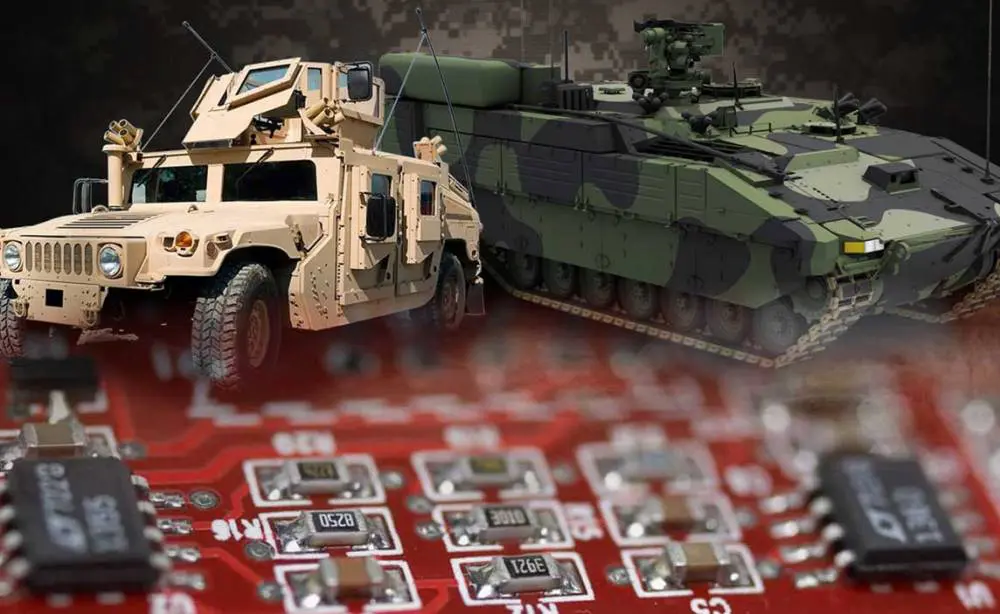
Top 10 PCB Assembly Manufacturers in USA

pcb assembly usa

Introduction

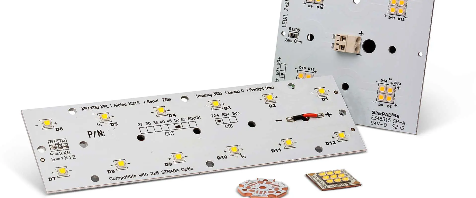
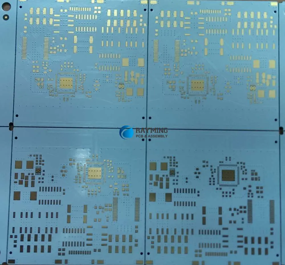
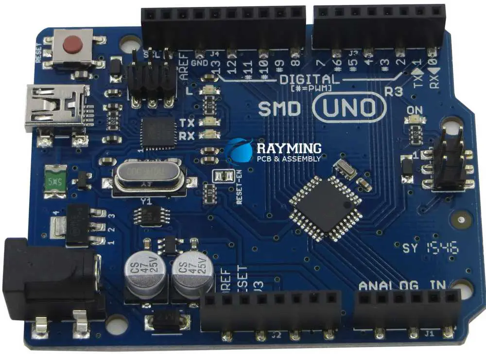
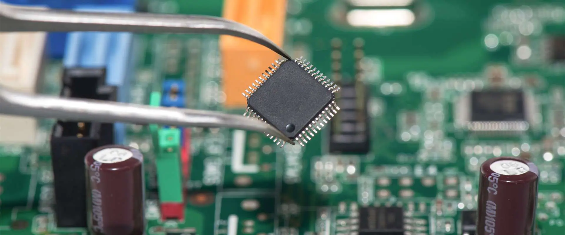
Printed circuit board (PCB) assembly involves soldering electronic components onto PCB substrates to create functional boards. As electronic products become more advanced, PCB assembly requires greater precision and technical specialization. This article explores the leading providers of PCB assembly services based in the United States.

We will examine major US-based electronics manufacturing services (EMS) companies focused on assembling PCBs. Key factors when selecting a PCB assembly partner include:

  • Technology capabilities โ€“ component sizes, BGA mounting, inspection systems
  • Quality and certifications โ€“ ISO, FDA, aerospace
  • Volume capabilities โ€“ prototype to high-volume production
  • Services โ€“ design support, procurement, test, box build
  • Technical expertise โ€“ engineering resources and specialty processes
  • Location โ€“ infrastructure proximity for supply chain control

This list focuses on US PCB assemblers with significant capabilities across these criteria. Letโ€™s explore the top American EMS companies for state-of-the-art PCB assembly.

Top 10 PCB Assembly Manufacturers in USA

1. Jabil

Jabil is a leading global EMS provider founded in 1966 and headquartered in Florida. They operate dozens of manufacturing sites worldwide including extensive PCB assembly capacity in the United States. Jabil offers the full spectrum of electronic product realization services for a variety of industries.

Locations: St. Petersburg, FL; Memphis, TN; Louisville, KY; and other global sites

Assembly Capabilities:

  • SMT and through-hole component mounting
  • 01005 components, 0.4mm BGA pitch
  • Advanced optical inspection and X-ray
  • Conformal coating, potting, injection molding
  • Box build, systems integration

Industries Served: Data networking, wireless, automotive, healthcare, instrumentation

Certifications: ISO 9001, ISO 13485, AS9100, ITAR Registered

Scale: Prototype to high-volume

With cutting-edge processes and huge capacity, Jabil provides advanced PCB assembly for major OEMs.

2. Flex

Flex is a large global contract manufacturer founded in 1969 and headquartered in California. They provide a range of design, engineering, and manufacturing services for electronics and other products. Flex operates an extensive advanced manufacturing footprint in the US.

Locations: Austin, TX; Fremont, CA; Milpitas, CA; and others

Assembly Capabilities:

Industries Served: Consumer, telecom, networking, automotive, medical, aerospace/defense

Certifications: ISO13485, ISO 9001, AS9100, ITAR

Scale: Low to high-volume

Flex offers diverse electronics manufacturing services for the complete product lifecycle.

3. Vexos

Vexos, founded in 1998, is an EMS company specializing in high-mix, low-volume complex assembly, including for the aerospace, defense, and medical sectors. Headquartered in Washington state, they provide precision manufacturing at their US facilities.

Locations: LaGrange, OH; Greenville, TX; Lynnwood, WA; and Markham, Ontario

Assembly Capabilities:

  • SMT and through-hole component assembly
  • System integration, box-build, cables
  • Design for manufacturing (DFM) expertise
  • Functional test solutions

Industries Served: Medical, aerospace/defense, industrial

Certifications: ISO 13485, ISO 9001, AS9100, ITAR

Scale: Low to medium-volume

Vexos delivers high-quality electronics assembly across regulated industries.

4. Honeywell Aerospace

Honeywell Aerospace stands out as a top avionics and aerospace PCB assembler, leveraging vertical integration to support aircraft OEM customers. Their advanced US facilities focus on aerospace and defense contractors.

Locations: Phoenix, AZ; Albuquerque, NM; Clearwater, FL; other global sites

Assembly Capabilities:

  • Mil-spec aerospace electronics assembly
  • Rigid and rigid-flex PCBs
  • System and box-build
  • Cable and wire harness assembly
  • Automated inspection

Industries Served: Avionics, space, defense

Certifications: AS9100, ITAR Registered

Scale: Medium to high-volume

Honeywell assembles aviation and high-reliability PCBs for the aerospace industry.

5. Plexus

Plexus specializes in producing electronic solutions for complex regulated industries. Founded in 1979, they focus on flexible, responsive manufacturing for medical, defense, aerospace, and industrial customers. Their specialized US facilities offer robust quality processes.

Locations: Neenah, WI; Lawrenceville, GA; Appleton, WI; and others

Assembly Capabilities:

  • SMT and thru-hole component assembly
  • Design and test support services
  • Microelectronics, box-build, cables
  • Supply chain and logistics management

Industries Served: Medical, defense, aerospace, industrial/commercial

Certifications: ISO 13485, AS9100, ITAR Registered

Scale: Medium to high-volume

Plexus services regulated sectors requiring rigorous quality standards.

6. Sanmina Corporation

Sanmina is a major EMS company founded in 1980 offering complete product realization services. They manufacture complex electronics including PCB assembly for leading OEMs. Sanmina operates large-scale manufacturing in regions including the US.

Locations: Fremont, CA; Sugar Land, TX; Huntsville, AL

Assembly Capabilities:

  • High-precision SMT and thru-hole assembly
  • System integration and test
  • Design support services
  • Box-build, cables, rack integration

Industries Served: Communications, industrial, defense, medical, automotive

Certifications: ISO 13485, ISO 9001, AS9100

Scale: Prototype to high-volume

Sanmina provides advanced assembly capabilities for tier 1 electronics OEMs.

7. Sparton Corporation

Sparton specializes in regulated medical and defense markets requiring complex subsystem devices. Founded in 1900, they provide design, development, and manufacturing including sophisticated PCB assemblies.

Locations: Strongsville, OH; Frederick, CO; De Leon Springs, FL

Assembly Capabilities:

  • Highly engineered PCB assemblies
  • Box-build and cable assemblies
  • Ruggedized and high-reliability
  • Complete product realization

Industries Served: Medical, defense and security

Certifications: ISO 13485, ITAR Registered

Scale: Low to medium-volume

Sparton services mission-critical regulated applications requiring specialized assembly.

8. SigmaTron

SigmaTron provides EMS focused on lower volume, higher mix assembly applications. Founded in 1993, they operate US plants supporting a diverse customer base across industries.

Locations: Elk Grove Village, IL; Union City, CA; Suzhou, China

Assembly Capabilities:

  • SMT, thru-hole, manual assembly
  • Conformal coating, potting
  • System integration, test jigs
  • Material procurement and supply chain

Industries Served: Industrial controls, communications, aerospace, appliances

Certifications: ISO 9001, IATF 16949

Scale: Low to medium-volume

SigmaTron services small and mid-sized OEMs with flexible assembly solutions.

9. Creation Technologies

Creation Technologies is an electronics and box-build assembler focused on low-to-medium volumes. Founded in 1991, they specialize in rapid prototyping and new product introduction (NPI) assembly services.

Locations: Tempe, AZ; Milwaukee, WI; Burnsville, MN; and globally

Assembly Capabilities:

  • SMT, thru-hole, and hand assembly
  • Clean room assembly
  • Component engineering
  • Functional test development

Industries Served: Industrial equipment, aerospace, telecom, medical, consumer products

Certifications: ISO 9001, ITAR Registered

Scale: Prototype to medium-volume

Creation Technologies supports low and medium complexity assemblies for R&D and NPI.

10. Ducommun

Ducommun is a Tier 1 supplier for major aerospace and defense OEMs. Founded in 1849, they offer advanced manufacturing capabilities tailored for regulated industries. Their expertise ranges from PCB fabrication through complex assembly.

Locations: Carson, CA; Guaymas, Mexico; other global facilities

Assembly Capabilities:

  • High-reliability SMT and thru-hole assembly
  • System integration
  • Cable and wire harness assembly
  • Enclosure machining and painting

Industries Served: Aerospace and defense

Certifications: AS9100, Nadcap, ITAR Registered

Scale: Medium to high-volume

Ducommun provides integrated aerospace and defense electronics solutions.

Comparing the Technical Capabilities

To summarize the key capabilities of these top American PCB assemblers:

CompanyLocationsAssembly TechnologiesIndustries ServedQuality CertificationsProduction Volumes
JabilFL, TN, KYSMT, BGA, test, box-buildVariousISO, ITARPrototype – high
FlexCA, TXSMT, press-fitConsumer, telecom, auto, medical, aerospaceISO, ITARLow – high
VexosOH, TX, WASMT, box-buildMedical, defense, aerospaceISO, ITARLow – medium
Honeywell AerospaceAZ, NM, FLSMT, aerospaceAvionics, space, defenseAS9100, ITARMed – high
PlexusWI, GASMT, thru-holeMedical, defense, aerospaceISO, AS9100, ITARMed – high
SanminaCA, TX, ALSMT, thru-holeCommunications, defense, medicalISO, AS9100Prototype – high
SpartonOH, CO, FLComplex PCB subassembliesMedical, defenseISO, ITARLow – medium
SigmaTronIL, CASMT, thru-holeIndustrial, aerospaceISO, IATF 16949Low – medium
Creation TechnologiesAZ, WI, MNSMT, hand assemblyIndustrial, aerospace, medicalISO 9001, ITARPrototype – medium
DucommunCA, MexicoSMT, systems integrationAerospace, defenseAS9100, ITARMedium – high

This comparison shows the diversity of advanced assembly services offered by premier US-based providers.

Factors in Selecting a PCB Assembly Partner

through-hole assembly process

Key considerations when choosing a PCB assembly partner include:

  • Technical capabilities โ€“ Fine pitch assembly, BGA mounting, smallest component sizes, inspection systems utilized.
  • Quality systems โ€“ ISO certifications, compliance with regulatory standards, reliability processes.
  • Volume โ€“ Prototype, low, medium, and high-volume production capabilities.
  • Lead times โ€“ How quickly assemblies can be delivered.
  • Location โ€“ Geographic proximity for supply chain control and IP protection.
  • Industry experience โ€“ Expertise in the application field.
  • Design support โ€“ Assistance with DFM, test development.
  • Customization โ€“ Ability to tailor services and production flow.
  • Cost โ€“ Assembly pricing, NRE charges.
  • Customer service โ€“ Responsiveness to requests and issues.

Evaluate PCB assembly partners holistically across these criteria to select the right fit.

Conclusion

This overview of the top PCB assembly manufacturers in the USA highlights premier American EMS companies serving diverse high-tech industries. Both large corporations and specialized assemblers provide quality manufacturing capabilities from prototypes through high-volume production.

Advanced electronics assembly requires an experienced partner to deliver high-yield, robust PCBs on schedule for your product development needs. Leveraging domestic US assembly can provide supply chain advantages for regulated, high-complexity, or quick-turn assemblies while accessing world-class manufacturing expertise.

Frequently Asked Questions

What are the main benefits of using a US-based PCB assembly manufacturer?

Benefits include supply chain control, protection of intellectual property, and meeting regulatory demands for domestic production and content for defense, government, aerospace, and medical applications.

What are the most advanced PCB assembly capabilities?

Cutting-edge capabilities include extremely fine-pitch components to 0201 or 01005 sizes, microBGAs under 0.5mm pitch, and specialized inspection systems like 3D AOI and x-ray.

How can assembly quality impact product performance and reliability?

High-quality assembly minimizes defects and rework to provide consistent product performance. Effective process controls, soldering, ESD control, and cleanliness are key.

What PCB assembly services typically accompany component mounting?

Additional services include solder paste printing optimization, cleaning, AOI, functional test development, rework/repair, conformal coating, potting, and box build integration.

What certifications are important for regulated industries?

Medical and defense assemblies often require ISO 13485, FDA registration for medical, AS9100 for aerospace, and ITAR registration for US defense contractors.

What are the Military Applications of Electronics?

Military Electronics

Introduction

Electronics technology plays a crucial role across nearly all aspects of modern military systems. Electronic systems provide capabilities that are essential for national defense and military operations.

This article explores how electronics are applied to enable key military capabilities. Weโ€™ll examine the roles of electronics for communications, surveillance, weapon systems, vehicles, identification, and other defense applications.

With continuous advancement in electronic systems, digital processing, and microelectronics integration, electronics will continue transforming the future battlefield and systems. Letโ€™s explore the vital current and emerging applications of electronics technology for military purposes.

Communications Systems

military-manufacturing-companies

Reliable communications are essential for coordinating operations between military units. Electronics technology enables various tactical and strategic communication links:

Radio Communications

  • Handheld radios for ground troop communications
  • Vehicle-mounted military radios with encryption
  • Airborne radios with frequency hopping spread spectrum
  • Wideband networked radios to transmit data
  • Software-defined radios for multi-waveform links
  • Satellite communication radios for global reach

Radios provide short and long-range wireless voice and data links between forces using the RF spectrum.

Cellular Networks

  • Deployable cellular infrastructure (cell towers)
  • Smartphones for multimedia messaging
  • Mobile command centers with 4G/5G connectivity

Cell networks enable secured mobile battlefield networks.

Wireless Data Links

  • Frontline sensor data receivers
  • UAV and drone command/control and live video downlinks
  • Wireless links between ships, aircraft, ground vehicles
  • Wi-Fi and mesh networks to connect forces

High-bandwidth wireless connectivity shares mission-critical data.

Underwater Communications

  • Submarine communication systems
  • Underwater acoustic modems for ship-to-diver links
  • Sonobuoys for underwater submarine signal monitoring

Sound wave transmission enables underwater communications.

Optical Communications

  • Line-of-sight ship-to-ship laser links
  • Short burst laser โ€œflashโ€ systems on the battlefield
  • Free space optics links from aircraft

Optical transmission provides very high bandwidth, secure lines of communication.

Military operations depend heavily on advanced electronic communications technologies to coordinate actions between units across land, sea, air, and space.

Surveillance Systems

Situational awareness of enemy positions and battlefield conditions is critical. Electronics enables various surveillance technologies:

Radar Systems

  • Ground-based air surveillance and fire control radar
  • Shipboard surveillance, navigation, and targeting radar
  • Airborne fire control, ground/maritime surveillance radar
  • Synthetic aperture radar (SAR) for high-resolution ground imaging

Radar utilizes radio waves to detect, locate and track targets.

Electro-Optical Sensors

  • Infrared cameras for night vision and heat sensing
  • High zoom daylight cameras for long-range observation
  • Multi or hyperspectral sensors to detect chemical agents
  • Image intensifiers and thermal weapons sights
  • Laser rangefinders and target designators
  • Night vision goggles and scopes for infantry vision enhancement

Advanced EO/IR sensors provide battlefield imaging and visibility.

Signals Intelligence

  • Radio and radar emissions surveillance
  • Communication link interception and decryption
  • Spectrum analyzers and direction finding systems
  • Encryption cracking computers

SIGINT monitors, intercepts, and obtains intelligence from adversary communication signals.

Reconnaissance Drones

  • Hand-launched mini-UAVs for local area visibility
  • Medium and high altitude long endurance UAVs with multi-day flight
  • Tethered aerostats for persistent regional surveillance
  • Swarming algorithms to coordinate drone networks
  • AI processing of sensor and image data

Unmanned aerial vehicles outfitted with sensors provide tactical reconnaissance.

Acoustic Sensors

  • Underwater hydrophones to detect submarine signatures
  • Gunshot detection systems
  • Battlefield microphones and seismic sensors
  • Aircraft and vehicle noise signature databases

Acoustic sensors detect and analyze sounds to reveal military activity.

Advanced electronic sensor systems deliver critical environmental awareness and targeting data.

Weapons Technologies

Military PCB Board
Military PCB Board

Modern militaries employ advanced electronics to enhance precision, effectiveness, and networking of weapons systems:

Guided Missiles

  • Radar and infrared guidance for long-range air-to-air, surface-to-air, and air-to-ground missiles
  • Laser beamriding guidance
  • GPS/INS guidance for cruise missiles
  • Imaging infrared seekers with target recognition
  • Data links between air controllers and missiles
  • Multiple independently targetable reentry vehicles (MIRVs)

Guidance electronics provide precision missile targeting and autonomy.

Artillery Systems

  • Gunner displays with ballistics computation
  • Integrated navigation, attitude heading reference systems
  • Automated targeting and fire control
  • Guided artillery shells with GPS and inertial guidance
  • Muzzle velocity radar to measure shell velocity
  • Meteorological and topographical sensors

Smart electronics assist accurate artillery gun laying and firing.

Armored Vehicles

  • Air defense radar warning receivers, laser warning systems
  • Thermal weapon sights and vision enhancement
  • Tank stabilized gun fire control systems
  • Autoloaders to mechanically reload tank barrels
  • Remote weapon stations for infantry fighting vehicles
  • Active protection systems to intercept incoming projectiles

Electronics enhance armored vehicle survivability, visibility, and lethality.

Smart Bombs

  • Laser and GPS guided bomb systems with moving target capability
  • Image recognition algorithms enable striking specific targets
  • Software defined radio controls alterations after launch
  • Networking between smart bombs for coordinated attack
  • Onboard autonomous target recognition

Guidance electronics allow accurate smart munition delivery.

Drones

  • Autopilots, flight control systems, and motors
  • Sensors like synthetic aperture radar and EO/IR cameras
  • Secure digital data links to ground control stations
  • Network technology to coordinate drone swarms
  • AI algorithms for autonomous target identification

UAV electronics enable unmanned aircraft with ISR capabilities or armed attack roles.

Advanced electronics transform weapons capabilities and lethality for the networked battlefield.

Vehicle Systems

Military Electronics

Military ground, air, and sea platforms depend on electronics for navigation, control, and subsystem integration:

Automotive Electronics

  • Drive-by-wire electronic engine and brake control
  • GPS navigation and in-vehicle awareness systems
  • Armored vehicle health and usage monitoring systems
  • EMI/RFI hardened automotive-grade electronics
  • Autonomous convoy driving algorithms

Automotive electronics enable networked combat vehicles.

Avionics Systems

  • Inertial navigation systems and GPS
  • Flight control computers and fly-by-wire
  • Heads-up displays and multifunction displays
  • Radar altimeters, terrain following radar
  • Distributed avionics architectures
  • Engine and flight data recorders

Avionics integrate critical flight and mission systems.

Naval Electronics

  • Phased array radars for ship defense
  • Electronic chart display and information systems
  • Thermal imaging systems for machinery monitoring
  • Ballast control systems for submarines
  • Integrated bridge systems for automation
  • Sonar systems for underwater detection

Marine electronics provide awareness, control, and automation.

UAV Avionics

  • Lightweight autopilots and flight controllers
  • MEMS inertial sensors and GPS receivers
  • Embedded computing payloads for image processing
  • Cloud connectivity and swarm coordination
  • AI autonomy for independent missions

UAV electronics enable unmanned aircraft flight and sensing.

Advanced military platforms require integration of diverse electronic subsystems.

Identification Systems

Identifying friendly forces is crucial in military operations. Electronics enables various identification technologies:

RFID Tags

  • Passive RFID tags worn by soldiers and attached to vehicles
  • Handheld RFID readers for proximity identification
  • Active RFID with longer read ranges for asset tracking
  • RFID triangulation for localization

RFID provides short range wireless identification.

IFF Transponders

  • Aircraft transponders responding to secondary surveillance radar
  • Automatic dependent surveillance โ€“ broadcast (ADS-B)
  • Cryptographic identification friend or foe (CIFF)
  • Selective availability anti-spoofing modules (SAASM) GPS

Avionics identification systems distinguish friendly aircraft.

Biometrics

  • Fingerprint, face recognition, and iris scanners
  • Hand geometry and palmprint readers
  • Speaker recognition systems
  • Behavioral analysis identification

Biometrics verify personnel identity biometrically.

Combat ID Systems

  • Vehicle mounted tag readers and transponders
  • Soldier worn tags
  • Blue force tracking GPS locators
  • Networked battle management systems

Tags and data links provide position location identification.

Electronic identification technologies help discriminate between friendly and hostile forces.

Soldier Systems

military PCB circuit board

Individual soldier systems utilize electronics to provide enhanced capabilities:

Tactical Computers

  • Ruggedized mobile computing devices
  • AI-enabled decision making and planning tools
  • Augmented reality headsets displaying mission data

Handheld computers assist ground forces with navigation, communication, and decision making.

Night Vision & Sights

  • Image intensification scopes and goggles
  • Uncooled thermal weapon sights and handheld viewers
  • Low light CMOS digital cameras
  • Laser aiming and illuminators
  • Wearable transparent displays

Digital night vision enhances visibility in low light conditions.

Body Armor & Exoskeletons

  • Embedded health and biometric monitoring sensors
  • Thermoelectric cooling and heating
  • Ballistic shock damping
  • Powered and load sharing exoskeletons

Smart armor protects and augments the soldier.

Hearables & Audio Processing

  • Bone conduction communications headsets
  • Noise canceling hearing protection systems
  • 3D audio recognition and localization
  • Voice command human-computer interfaces

Advanced audio systems aid communications and situational awareness.

Power Sources

  • Lightweight batteries with high energy density
  • Solar charging systems
  • Energy harvesting from soldier motion
  • Compact fuel cells

Portable power sources energize soldier electronic systems.

Electronics aid dismounted forces with enhanced sensing, computing, and communications.

Trends in Military Electronics

Many technology trends are shaping the evolution of electronics for military purposes:

  • Ubiquitous sensing with miniaturized MEMS sensors
  • Artificial intelligence for data processing and decision making
  • Autonomy enabling unmanned systems
  • Additive manufacturing to produce electronics and parts
  • Flexible hybrid electronics manufactured on fabrics
  • More electric technologies and conversion from hydraulics and pneumatics
  • Nanotechnologies for ultra-small sensors and electronics
  • Higher frequency electronics like millimeter-wave radar
  • More powerful embedded computing resources
  • Everything connected โ€“ the Internet of Military Things

These trends will transform how militaries leverage electronics to gain a tactical edge and field increasingly advanced capabilities using smart systems.

Conclusion

In summary, electronics technology plays an indispensable role across nearly all aspects of modern defense systems. Electronics provide critical advantages in communications, surveillance, target acquisition, weapon systems, vehicles, identification, soldier systems, and computing capabilities.

Continued research and development will further integrate electronics to create a more networked, information-driven, instrumented battlefield. The precision, automation, awareness, and coordination enabled by military electronics will continue to evolve warfare capabilities.

Frequently Asked Questions

How has electronics impacted the evolution of military systems?

Electronics have enabled modern militaries to field very advanced communications, sensor systems, precision-guided weapons,satellite navigation, and networked coordination that were not possible with purely mechanical systems.

What are some examples of cutting edge military electronics research?

Areas like phased array radars, directed energy weapons, hypersonic technologies, advanced stealth materials, quantum sensing, AI-enabled systems, and augmented reality are pushing the boundaries of military electronics.

Which fields of electronics research are important for defense applications?

Key areas include radio frequency electronics, embedded computing, digital signal processing, microelectromechanical systems, nanotechnology, automation, robotics, and artificial intelligence.

What new capabilities might future military electronics enable?

Future systems may feature directed energy weapons, large drone swarms with AI cooperation, railguns with power electronics drives, augmented reality heads-up displays, smart dust sensor networks, and increasingly autonomous robotic systems.

What challenges constrain applying advanced electronics to military systems?

Technical challenges include operation in extreme environments, security, reliability, Size, Weight and Power (SWaP) restrictions, radiation tolerance, and cyber vulnerabilities that must be overcome to field cutting-edge military electronics.

How to Realize a Fine Pitch PCB Assembly

pcb pitch

Electronic circuit designers have to consider plenty of things designing a printed circuit board. It becomes critical to consider the type of PCB to design, but design components such as the components, separation of ground levels (if it incorporates a hybrid of digital and analog PCB), placement of components, among many other considerations. However, one key aspect that every designer needs to take into consideration entails pitch size. In this article, I will detail fine pitch PCB and its assembly process.

A Brief about Fine Pitch PCB

A fine pitch PCB implies printed circuit boards having a considerably high number of components for every square inch. Therefore, components prove close together with the board’s design guidelines pushing the fabrication limits of the printed circuit board fabrication. A fine pitch PCB also gets inferred as a high-density PCB.

Before we get into the design and assembly process, it becomes imperative to understand a few things about high pitch PCBs, especially regarding crucial components.

  • Screw terminal 2.54 mm pitch. The screw terminal component is crucial and comes as a simple two-position screw terminal containing 2.54mm pitch pins. Such a pitch allows it to align with the typical 0.1-inch perf boards.
  • 2.54 mm screw terminal blocks. It comes as a side-entry screw terminal block and contains a 2.54mm or 0.1-inch pitch. It can become an excellent alternative to the typical 0.1-inch female or male headers that most printed circuit boards feature. The reason this becomes possible entails the terminals proving capable of releasing and holding wires through adjustment of screws, which allows for temporary connections to the PCB.
  • 2.54mm terminal blocks. The 2.54 terminal block is an important component in a PCB that helps keep loose wiring in check when making PCB-to-wire connections. The spacing allows them to fit perfectly into breadboards (solderless).
  • Veroboard pitch. It implies a 2.54mm hole size drilled into the copper track rows that feature this PCB design.

It becomes crucial to understand what these terms imply as you will constantly encounter them in the fine pitch PCB assembly process.   

How to Design a Fine Pitch PCB

2.54 mm screw termina

Fine-pitch components always become a common feature for high-density applications and often drive up production capabilities and cost. If a component is smaller, the pads also become small, and thus, will necessitate the need for the place and pick machines to prove accurate. However, when deploying grid-array and leadless-based components, it becomes essential to carry out x-ray inspection when assembling.  

As a designer, it becomes imperative to develop a closely-knit relationship with the PCB manufacturer/assembler to help you come up with a fine pitch PCB. It becomes essential because plenty of the details and decisions will depend on the facilities available on the assembly company. Your printed circuit supplier has to furnish you with broad guidance regarding risks, especially from CAM operators, among other technical representatives from board houses.  

At RayMing PCB and Assembly, our support and engineering teams will guide you in ensuring that the realization of top-quality results becomes feasible, primarily in assembly and manufacturing. For any inquiries, please check our homepage and get in touch with us.   

Designing often requires a layout, something that a designer must think through carefully before starting the design process. Otherwise, it becomes easy to get trapped into the numerous pitfalls that can render your design inefficient. So what are some of these potential pitfalls you can face?

Potential Fine Pitch Layout Problems and Important Steps to Avert Them

The layout process of hundreds of PCB components within a small limited space can prove daunting and complex. In most cases, it will require plenty of trial runs to avert pitfalls and issues. Below, some of the crucial pitfalls to avoid.

  • Misplaced or unplaced components from the schematic
  • Overpopulated the PCB without adequate room for trace design
  • A lack of consideration for isolation and high-speed traces
  • Lack of compactness

It, therefore, becomes essential to carry out the design process process-wise and below the process.

  • Component selection. Firstly, it becomes pivotal to select small components to ensure they fit within the limited board space when placing. However, it can always become a careful balance between saving the board space and saving costs.  

Remember, it always proves costlier to assemble finer pitch components, especially when they have to get populated. It becomes more arduous when the components need a particular inspection like the ground array, which relies on x-ray inspection.

The cost always shoots when tolerances become tighter, and you have to get your priorities right. For instance, if you want to save or cut costs, picking larger components might prove ill-advised. Most integrated circuits come complete as a package, and it could prove useful to consider the datasheet when populating your schematic.

Component ratings should also guide your selection of components. It represents another crucial aspect that needs consideration for every component. Additionally, a balance needs to get created and weigh the desired margin to build components like capacitors concerning package size.

  • Board size. It comes as the subsequent step after the component selection in assembling the PCB. Here, you have to define a reasonable board size for starters. Additionally, based on the existing mechanical constraints, a dimensions limit might become important, especially on the Z, X, or Y due to the environmental variables. If, for instance, the board’s mechanical details are under development and the size proves negotiable, then the process becomes easier.  

Characteristically, the size of the board will direct the needs of the mechanical hardware. You, therefore, have to specify and verify the size of the targeted board to the mechanical unit responsible for the assembly. However, it becomes crucial to check the potential usefulness of the small board. It can get accomplished by placing bulky components, outside connectors, and large integrated circuits that need extra surrounding room to break signals. All of these consider sensitive traces besides their isolation or separation from the other components of the board. It becomes easier to save costs by selecting pre-set board shapes/sizes like fitting plain square shapes with particular dimensions.

Important considerations to make at this point include clearances, trace width, and vias proportions. However, remember the importance of concessions, especially when it comes to costs. With the determination of the fine-pitch integrated circuits by this point, the requirements then get defined. Remember, the fine-pitch IC determines the design needs. For instance, a 0.4mm ball pitch BGA component needs the specs fulfillment of the same to function seamlessly. Whenever you want to use a high-speed integrated circuit that needs differential pairs besides impedance control, a vendor has to get reviewed. For instance, a connector may require diverse odd-shaped slots and may subsequently under the custom capability.

  • Component placement. At this point, the placement of component start and includes fitting them close together but with sufficient room vias, traces, planes, etc., and proves more of a trial process until completed.

Firstly, placement starts with high-speed and high-power components besides connectors and extra mechanical components. Once placed, you get an established framework to start working from. Considerations when it comes to fine pitch design optimization of the board space, you have to consider the following.

  • Via-in-pads. It comes as a non-recommendation from assembly houses, though one can free up some space between tightly-spaced components for the traces. It especially entails establishing vias on component pads, and these come as capacitors, resistors, ICs, etc., to conserve the routing room. Nonetheless, a risk exists that components may not receive enough solder connection due to the surface area the โ€œviaโ€ consumes. ย ย ย 
  • Decoupling capacitors. It mostly gets placed on top, near, or below sensitive pins. Placement becomes critical on the PCB. However, these decoupling capacitors might end up occupying plenty of routing/board space. It sometimes happens that some of the capacitors get left out, and this adds the risk of noise on sensitive digital/analog signals. However, the risk may prove minimal.
  • Fiducial marks. Incorporating these image system’s guide markers allow the machine (pick and place) to identify the location of the printed circuit board. A 1mm diameter circle atop the copper layer (devoid of solder mask) is commonly incorporated at the PCBโ€™s corners. While not necessarily required for the printed circuit board assembly, it helps with the placement precision when the vendor assembles. ย ย ย ย ย 
  • Tooling holes. It represents a crucial and useful addition to the testing and assembly process of PCBs. It helps align drilling holes, solder stencils, text fixtures, and pick and place equipment. Tooling holes can become instrumental for board mounting into an enclosure. ย 
  • Special modifications. Reducing the volume that odd-shaped and bulky components occupy makes it important to trim off a component’s segment by trimming. Such segments may entail needless metallic shields and component protrusions.
  • 3D parts. It becomes possible to import comprehensive connector and extra mechanical-based part’s step files to allow for precision planning and placement. It allows for the depreciation of clearance between the board edge and the parts pads.
  • Test points. It also becomes critical to remember the capacity of testing every signal that gets related to the fine-pitch components. ย 

Final thoughts

It always becomes pivotal to balance the complexity and cost aspects regarding printed circuit board assembly and fabrication besides understanding that the concessions can save you time and money during the product’s production and development. Hopefully, this piece has answered some pertinent fine pitch PCB assembly issues you might have had. However, in case of further inquiries, go to our homepage and get lodge your questions.   

What is MCPCB โ€“ Metal Core Printed Circuit Board

MCPCB

In recent years, there has been great popularity in the use of LED products. This is why mcpcbs – metal core printed circuit boards have also gained popularity. The lighting and automobile sectors have already accepted the technology, same way consumers have. This is because an LED light can prove to be five times less expensive compared to the incandescent unit. Also, compact fluorescents seem to have a little higher cost for operating and when we talk about using space efficiently, they donโ€™t have what it takes to compete with very small LEDs.

Due to these, as well as other factors, many other devices have started incorporating LEDs as one very important design feature. However, there is a very important aspect of operation of LEDs, which has to be accounted for whenย handling product designs; that is heat.

What is a Metal Core PCB (MCPCB)?

MCPCB, which is also referred to as a metal backed PCB or thermal PCB is a PCB having its base material as metal for the boardโ€™s portion that spreads heat. This thick metal, which is always copper or aluminum in most cases, is covering one of the PCBsโ€™ sides. This metal core has to do with the position of the metal, whether it is in the center or middle or on the mcpcb boardโ€™s back.

The main task of the MCPCBโ€™s core is to help in redirecting heat from board components that are critical in nature as well as areas that are less crucial like the metallic core. MCPCBโ€™s base metals usually serve as an option to CEM3 or FR4 boards.

Thickness and Materials of Metal Core PCB (MCPCB)

MCPCB Board

The thermal PCBโ€™s metal core could be aluminum, copper, or a combination of different special alloys. For the aluminum type, it is called aluminum core PCB, which is the most commonly used. While for the copper type, it is called either heavy copper PCB or copper core PCB.

Some other materials, such as steel or brass, are requested sometimes, however, they are usually not recommended. The materials of the metal PCB are usually very hard. This is why cutting these PCBs to get smaller pieces could pose some problems. There are other things to consider when choosing materials for a metalย PCB. These include the chemicals used during manufacturing and if there will be a reaction of the metal to them.

The metal coresโ€™ thickness, which is found in the plates of the PCB base usually falls between 30 mil to 125 mil. However, it is possible to have thinner and thicker plates. The thickness of the copper foil of MCPCB can fall between 1 to 10 oz.

Benefits of MCPCB

In so many scenarios, LEDs are similar to all other components that can be mounted on or attached to a circuit board. The fact is that if just a few LEDs are available like red and green indicators, then whenever you are laying out the PCB, the reason to do something unusual will be little. However, lighting solutions which integrate either arrays or rows of MCPCB LEDs are available. This stays on for a long time period.

Ensuring that these devices are kept cool to prevent them from failing prematurely, as well as creating a safety hazard could become a major problem. Cooling it efficiently is also necessary to ensure that there is a consistent light output. Converting your PCB to a MCPCB from the standard type (FR4)is also a good alternative to consider.

Some benefits of metal core PCBs is its use of unique substrate materials that are formulated specifically to help in improving the designsโ€™ reliability, which run at temperatures that are above normal

Rather than serve as just a surface for mounting for these components, these substrates help in drawing heat actively from areas where the components are hot-running via the mcpcb boardโ€™s opposite layer,  where dissipation can be done safely and efficiently.

MCPCB has proved to be a great solution to problems concerning the cooling of PCBs using a large number of LEDs.

Applications of Metal Core PCBs

Applications generating much heat frequently cannot be cooled adequately making use of traditional fans only. Cooling done conductively via MCPCBs are a great option for production.

Most times, MCPCBs are seen in LED technologies. This is because they require less LEDs to give a desired illumination. Diodes that emit light release heat in great amounts in applications like:

  • Back light units
  • Street safety such as lighting, streetlights, etc.
  • System automotive
  • Electric/hybrid motor control
  • General lighting
  • Photovoltaic
  • Power converters such as power supplies, regulator of high voltage, industrial, telecom

Some other applications, which are great for integrating MCPCBs include motion control and solar panel applications.

Differences Between MCPCBs and Standard Epoxy Glass Boards

FULL PCB MANUFACTURING Quote

One great difference to comprehend between MCPCB and standard PCB is the working of the materials together to help achieve the result desired. In a MCPCB LED, we have one circuitry copper foil layer that is bonded and linked to a dielectric material that is thermally conductive.

The measurement of the thermal conductivity of a dielectric material is in W/mK – watts per meter, Kelvin. A rating of 2.0W is usually common; this type of material is usually approximately six to seven times thermally conductive like FR4.

The best practice here is keeping this dielectric layer very thin. By doing so, this builds the shortest path possible from the source of heat to the backing plate of the metal which is far more thermally conductive compared to dielectric materials. Majority of materials usually come in different thicknesses. This usually falls between 0.003 inches and 0.006 inches. You will not have too many opportunities or chances to specify a thicker material, which could reduce the materialโ€™s effectiveness to perform its function of thermal transfer.

The backing plate, which is utilized on the bottom, is seen as the structureโ€™s thickest element. This can be found in different thicknesses. However, it is advisable that you use any of the three common types (3.2mm, 1.5mm, and 1.0mm). This is because these types are very easy to buy; thereโ€™s no delay. Also, its metal layer ensures the circuit is kept flat, adds rigidity, and makes sure that enough thickness is added. This is to ensure that the MCPCB will be able to utilize the mounting hardware used for other circuit board with standard thickness. The boardโ€™s metal plate area does not accept soldermask or surface finishes.

Metal Core PCB Surface Mounted Components

One important factor to integrate into any design of MCPCB is using just surface-mounted components rather than use plated through holes. Majority of LED PCBs that are built on FR4 substrates with more than two layers must utilize a plated pattern that is closely-spaced through vias. During assembly, solder can find its way or migrate through the vias, if they are not properly filled. This will lead to an imperfect solder joint.

Using MCPCB, the function of vias is achieved by the materials. The whole section of the bottom is made up of metal having an efficient and higher thermal conductivity. This enhances the cooling and thereโ€™s no need for vias to get thermal relief. Majority of MCPCBs only need minimal drilling, a few mounting holes that are large.

Removing via drilling coupled with the ability of stacking more than one panel for drilling large holes simultaneously, makes it possible for the fabricator to quickly move your boards via a bottleneck operation. After a drill cycle, your MCPCB (1-layer) avoids the deposition of graphite or electroless copper deposition hole wall step, which would be necessary for the PTH processing. It then progresses to circuitย imaging. Then, from this point, your MCPCB works with fewerย or more process steps, which standard FR4 designs should follow.

Comparing the MCPCB with the FR4 PCB

Conductivity: The thermal conductivity of FR4 is low. It stands at around 0.3W. For MCPCBs, their thermal conductivity is higher. This ranges from 1.0W to 4.0W. Most times, this value stands at about 2.0W.

Plated Through Holes: Usually, FR4 PCBs make use of plated through holes. However, In MCPCB, you cannot have plated through holes for a 1-layer PCB. This is because all its components are usually surface-mounted.

Thermal Relief:  For FR4 PCB, the thermal relief involves vias to ensure heat transfer. With a longer drill cycle, many processes are added. MCPCB materials give their own thermal relief. The processes of via drilling, plating, and deposition are eliminated.

Solder Mask: The solder masks of FR4 PCB are usually dark colors (black, blue, red, green). They are usually applied at the bottom and top. For MCPCB, their solder masks are usually white. They are only applied to the top.

Thickness: The FR4 PCB features different thicknesses, which are available with the use of different layer counts and material combinations. The thickness variation of the MCPCB is limited by the thickness of the dielectric sheet and the available thicknesses of the backing plate.

Conclusion

MCPCB, is a PCB having its base material as metal for the boardโ€™s area that spreads heat. MCPCBs use unique substrate materials that are formulated specifically to help in improving the designsโ€™ reliability. MCPCB has proved to be a great solution to problems concerning the cooling of PCBs using a large number of LEDs.

High Quality 24 layer PCB Manufacturing

24 layer pcb

A 24-layer PCB falls under the multi-layer PCBs. And as the multi-layer name suggests, it indicates a circuit board with more than two layers. With the increase in connectivity and access to electronics, there is a high demand for PCBs. It makes the demand for multi-layer PCBs high also. Large industries such as consumer products, military, healthcare equipment, and technology devices drive 24 Layers PCB Manufacturers to position themselves to meet the ever-growing demand.

We have a blend of abilities among fabricators identified with production capacities and the quantity of 24 PCB layers that they can deliver. Assembling of 24 layer PCBs includes an interaction of consolidating different layers of core and prepreg materials into one unit, using high pressure and heat to guarantee proper curing of adhesives, elimination of air between layers, and uniform encapsulation of conductors that bind the layers together.

Because of the different layers of material, the execution of drill openings among layers should be painstakingly recorded. It is significant to assemble multi-facet PCBs that designers consolidate even format across layers to help abstain from a bow or twisting in the materials when pressure and heat factors are applied.

While sourcing a 24 Layers PCB Manufacturer, get the manufactureโ€™s standard tolerances and capabilities for these complex PCBs. Use manufacturing design procedures to accommodate those principles. It helps build certainty that the outcome will meet all performance, functional dependability, and execution assumptions.

24-Layer <a href="https://www.raypcb.com/how-to-plan-multilayer-pcb-stackup/">PCB Stackup</a> Selector

24-Layer PCB Stackup Selector 24LEXTREME

Configure layer thicknesses for extreme-density 24-layer datacenter, HPC, AI/ML accelerator, 800G networking, and advanced backplane PCB designs

Quick Presets

Layer Assignment (12 Signal + 6 GND + 6 PWR)
L1 SIG
L2 GND
L3 SIG
L4 PWR
L5 SIG
L6 GND
L7 SIG
L8 PWR
L9 SIG
L10 GND
L11 SIG
L12 PWR
L13 GND
L14 SIG
L15 PWR
L16 SIG
L17 GND
L18 SIG
L19 PWR
L20 SIG
L21 GND
L22 SIG
L23 PWR
L24 SIG

Copper Layers (24)

Prepreg Layers (12)

Core Layers (11)

Total Board Thickness
4.000mm
4000 ยตm
vs 4.0mm
+0 ยตm
Copper (24L)
840 ยตm
Prepreg (12L)
1482 ยตm
Core (11L)
2000 ยตm
12
Signal
6
GND
6
PWR
10
Stripline

Stackup Visualization

Outer SIG
Inner SIG
GND
PWR
Prepreg
Core
๐Ÿ’ก 24L Targets
3.5mm: High-density HDI
4.0mm: Standard 24L
4.5-5.0mm: Server/HPC
5.5-6.0mm: Backplane
๐Ÿ“ Impedance
Microstrip: L1โ†’L2, L24โ†’L23
Stripline: All inner SIG
Center: L12โ†”L13 PWR/GND pair
โšก Power Integrity
6 GND: Every 4 layers
6 PWR: Multi-rail splits
L12-L13: Ultra-low Z pair
๐Ÿ”Œ Applications
AI/ML: GPU/TPU modules
Network: 800G switches
HPC: Supercompute nodes
๐Ÿ”ง 24-Layer Design Strategy
12 Signal Layers: L1, L3, L5, L7, L9, L11, L14, L16, L18, L20, L22, L24 โ€” Maximum routing density for ultra-fine-pitch BGA (0.25mm), HBM3/HBM3E, 224G PAM4 SerDes, PCIe Gen6, CXL 3.0, and UCIe interfaces.
6 GND Planes: L2, L6, L10, L13, L17, L21 โ€” Ground reference within 3-4 layers of every signal; symmetric distribution minimizes return path inductance and EMI.
6 PWR Planes: L4, L8, L12, L15, L19, L23 โ€” Support 8+ voltage rails with island splits; L12-L13 form ultra-low-inductance decoupling capacitor structure.
Sequential Lamination: Requires 3+ lamination cycles with blind/buried vias, stacked/staggered microvias, and potentially ELIC (Every Layer Interconnect).
Materials: Ultra-low-loss required (Megtron 7, Tachyon 100G, I-Speed, EM-890K) for 56Gbps+ channels. Dk ~3.0-3.3, Df <0.002.
Symmetry: Structure symmetric about L12-L13 center for optimal CTE matching, <0.4% warpage, and reliable assembly of large BGAs/LGAs.

Balancing PCB design layers

24 layer pcb design

The plan of multi-layer printed circuit sheets can be exceptionally complex. A design even necessities to utilize multiple layers infers that the necessary number of circuits will not fit onto simply a top and a base surface. Even when the hardware fits onto two outside layers with no issue, the PCB creator may add force and ground planes inside to address an exhibition weakness.

A wide range of components can make a circuit perform not exactly ideally, from heat issues to complex EMI or ESD issues that should be pursued down and disposed of. Be that as it may, while as a manufacturer, your main concern is to address the electrical problems, it is similarly as significant not to dismiss the boardโ€™s actual design. A 24-layer PCB electrically impeccable may, in any case, bow or wind, making gathering troublesome or even inconceivable. Luckily, consideration paid to the PCBsโ€™ actual setup during the planning cycle will limit assembly migraines later. Layer-to-layer balance is one of the critical parts of a precisely strong circuit board.

PCB Thickness Issues

While twist and bow are the most widely recognized quality issue that happens when your 24 layer PCB stackup is not adjusted, there is another condition that can cause questions at conclusive investigation. This condition is welcomed by a minor plan oversight and is moderately uncommon. However, it can occur if your format includes reliably uneven copper inclusion for a similar area on a few layers. For the most part, it is seen on PCBs that use at any rate 2-ounce copper and generally high layer checks. What happens is that one feature of the board has a critical space of poured copper, while the other area is moderate without copper. When the layers are covered together, the side with the copper pushes down to one thickness, while the side with light or no copper closes squeezes slenderer.

Most PCBs that utilization half-ounce or 1-ounce copper will not endure a lot. However, the thickness failure with heavier copper can be critical. If you have, for instance, eight layers of 3-ounce copper, the zone with the lighter copper inclusion can undoubtedly fall beneath the general thickness resilience. To avoid this, make certain to pour your copper as uniformly as you can across the layer surfaces. If it is not reasonable because of either electrical or weight concerns, then add some plated-through openings to the light copper zone and make certain to remember cushions for the openings for each layer. These pad/hole constructions will offer mechanical help in the Y hub, decreasing the deficiency of thickness.

PCB Dielectric Layer Thickness

It is likewise acceptable practice to adjust the dielectric thicknesses all through the stack. The thickness of every dielectric layer ought to, in a perfect world, be reflected in a way manner that the layer types are reflected. When the thicknesses are not the equivalent, it tends to be hard to show up at a material set that will fit simple production. Occasionally an asymmetrical stack-up is unavoidable because of a component. For example, an antenna trace that requires an uncommonly enormous distance among it. Its reference plane yet makes certain to investigate and debilitate any remaining choices before pushing ahead. Most manufacturers will demand an unwinding waiver of the twist and bow resilience when lopsided dielectric partitions are required. It may even leave the work on the off chance that they cannot get such a waiver. They would prefer not to wind up reconstructing a few expensive clumps at low yield before at long last getting sufficient great units to fulfill the first request amount.

Circuit Board Cross-Section

One normal plan-related explanation that a 24-layer PCB will not completely accept is that its cross-sectional design is not even about its middle. For instance, if an 8-layer configuration utilizes four sign layers or fractional planes with moderately-light copper inclusion over the middle, and four generally strong planes beneath, then the pressure applied by one side of the stack compared to another will presumably make the whole stack twist.

It is along these lines great practice to plan the stack-up, so the sort of copper layer is reflected according to the middle. The top and base layer types match, as do those for L2-L7, L3-L6, and L4-L5. The copper inclusion is probably similar on every sign layer, and the plane layers comprise strong poured copper. Assuming this, the board has a decent opportunity to get done with a level, even surface ideal for robotized gathering.

A Balanced PCB Stack-Up

A decent 24-layer PCB stackup is one in which both the layer surfaces and the cross-sectional design of the printed circuit board are sensibly even. The objective is to eliminate regions that could twist when exposed to the burdens of creation handling, especially at the overlay stage. At the point when a circuit PCB deforms, it can turn out to be hard to assemble. It is particularly valid for sheets gathered on a robotized surface mount pick and spot line. Twisting could even hamper the establishment of the populated PCBA into the eventual outcome.

IPC investigation measures ought to forestall the most genuinely twisted to bowed boards from truly showing up at your office. In any case, if the PCB fabricatorโ€™s cycles are not uncontrollably crazy, the main driver of most bow and curve ends up being configuration-related. Hence, you should perform an exhaustive audit of the PCB design and make any vital changes before putting in your first model request. Doing so may forestall a bad yield.

Advantages of Multilayer Printed Circuit Boards

Most 24 Layers PCB Manufacturers are discovering the interest for multi-facet board expanding huge amounts at a time. This developing interest is taken care of by the requirement for more modest, lighter sheets for electrical gadgets, military hardware, medical services, and an extending market for smart gadgets fused in-home robotization frameworks.

Cell phones and PCs are ideal applications for 24-layer PCBs, requiring conservativeness and lightweight yet modern usefulness.

From a specialized outlook, there are various benefits to the utilization of multi-facet plans, far beyond saving space and weight:

  • Multilayer PCBs can be produced in both unbending and adaptable development. Be encouraged, however, that the more layers joined in a flex PCB, the less adaptable it becomes.
  • Connectors needed for different separate PCBs are decreased or dispensed with, improving development and further lessening weight.
  • Higher thickness of assembly.
  • By their natural electrical properties, multi-layer sheets give high limits and rapid in a more modest impression.
  • Manufacturing measures for multi-facet sheets bring about top-notch, solid results.
  • By joining different layers in a solitary PCB, sheets can build usefulness.

Disadvantages of Multilayer PCBs

Each innovation has upsides and downsides, and multi-facet PCBs are not safe from negative credits:

  • Interconnection between layers is critical for board work, making plan and manufacture of micro vias and large thickness basic.
  • Repairing a multi-layer PCB can be incredibly troublesome and may even be impractical or incomprehensible. It makes the failure of a multi-facet board exorbitant since it might be completely supplanted.
  • With expanded usefulness comes the requirement for more comprehensive testing of a solitary PCB. Assembling cycles may likewise be longer because of the actual intricacy of the assembling interaction.
  • The compactness of multi-facet sheets produces configuration worries for such issues as crosstalk and impedance issues.
  • Service accessibility โ€“ not all PCB makers have made the obligation to assembling these complicated boards, restricting the asset alternatives accessible to PCB creators.
  • Cost โ€“ one of the essential negatives in planning and executing multi-facet PCBs is the expense. As specific cycles are associated with assembling these sheets, there is extensive speculation needed for fabricators to offer these administrations. It makes the expense of multi-facet sheets higher than a conventional single or two-fold-sided board.

Summary

Focus on both electrical execution and actual construction when planning and spreading out a 24-layer PCB, regardless of whether you need to bargain marginally on the two viewpoints to show up at a general plan that is both practical and manufacturable. As you gauge your alternatives, remember that a plan with exceptional electrical qualities will not be beneficial if it is troublesome or difficult to populate with parts under deformity as bow and curve. Equilibrium your 24-layer PCB stackup and focus on copper dissemination on the different layers. It means to improve the probability that you will wind up with a board that is not difficult to collect and introduce.

How to Get Arduino PCB – Everything You Need to Know

Arduino PCB

The Arduino circuit board is gaining popularity in the PCB industry over time. Many electronic engineers built their prototype with the Arduino PCB. Engineers use the Arduino PCB in several applications due to the benefits and features it offers.

Arduino PCB has been the brain behind the production of various pieces of equipment over the years. You might be wondering what Arduino PCB is all about. In this article, we will be discussing what Arduino PCB does, its features, benefits, applications, and limitations.

What is Arduino PCB?

Arduino is a type of printed circuit board that is an open-source platform. These circuit boards are utilized in developing electronics projects. These boards are based on easy-to-use software and hardware. They comprise a physical programmable board known as a microcontroller and software. Arduino boards are utilized to write and upload computer code to the physical board.

Arduino PCBs can read inputs such as a finger on a button or a Twitter message and transform it into an output like activating a motor. You can send instructions to the microcontroller of the board to tell it what to do.

Arduino PCBs have become popular due to the growing demands in the electronics industry. The Arduino is distinct from other programmable boards as it doesn’t require a separate piece of hardware to input new code onto the board. Furthermore, the Arduino software (Integrated Development Environment) utilizes a version of C++ which makes it easy to learn programs.

Arduino also offers a standard form factor that simplifies the microcontroller’s functions into a more accessible package. Arduino PCBs can be used to design digital devices with sensors and control systems. These boards are reliable for designing simple or complex devices.

Arduino was developed for non-engineers to have access to easy-to-use and low-cost tools for developing hardware projects. This board is launched under a Creative Commons license, allowing people to design their boards.

What is the Function of Arduino PCB?

arduino circuit board

The Arduino PCB was specifically designed for hobbyists, artists, newbies, hackers, and designers who want to create interactive objects. Arduino boards interact with cameras, LEDs, motors, buttons, speakers, mobile devices, and television among others.

The Arduino software and hardware are easy to learn. Due to this, a good percentage of users have contributed code and given instructions for several Arduino-based projects. Arduino serves as the brain behind most electronic projects. The USB cable from your computer can be used to power Arduino boards.

Arduino PCB contains voltage regulator, Main IC, USB, Rest button, Analog, and digital pins, ATmega Microcontroller, and power indicator LED. This board features a flash memory of 32 kilobytes for storing your code. Arduino microcontrollers are sensitive to the environment. It receives input from various sensors.

Arduino functions in several applications. They are used in designing prototypes and developing code-based control. This circuit board is also ideal for creating basic circuit designs.

Types of Arduino Boards

There are several types of Arduino Boards and each of these boards has distinct features, specifications, and uses.

Lilypad Arduino

This type of board is specifically made for integrating with e-textile and wearable projects. The Lilypad Arduino is round-shaped and helps to reduce snagging. It connects easily to other devices.

It utilizes the Arduino bootloader and Atmega328 microcontroller. Lilypad Arduino utilizes large pin holes to help them connect to other devices easily. It is commonly used to control various devices like light, switch, and motor. The components of Lilypad are washable since it is applicable in clothing industries.

Arduino Leonardo

This is a type of Arduino board that utilizes Atmega 32u4 in it. Arduino Leonardo comprises 20 digital output pins and input in it. This Arduino PCB board has one power jack, RESET button, and micro USB connection in it.

You can fix this board to a computer system through a USB connection. An AC or DC adapter can provide a power supply to this board. Arduino Leonardo uses a microcontroller that features an in-built USB connection. This connection eliminates the reliability of the extra processor in it. This type of Arduino is the cheapest.

Arduino UNO

Arduino UNO is one of the most recent Arduino boards. This type of board has various features that help users in their projects. It utilizes the Atmega 16U2 microcontroller. This increases the rate of transfer. The Arduino UNO board doesnโ€™t require extra devices such as a keyboard, joystick, and mouse among others.

The Arduino UNO features SDA and SCL pins and two extra pins. This board comes with 14 digital output pins and input pins. 6 pins serve as analog inputs while another 6 pins serve as PWM. Arduino UNO can be fixed to the computer system through a USB port. This circuit board has 32KB flash memory.

Arduino Shields

This type of Arduino board serves as pre-build circuit boards that connect other Arduino circuit boards. Arduino shields are mounted on Arduino boards. They boost the capability of the board to be connected to the internet. They also control the motor, LCD, and establish wireless communication.

Arduino Mega

The Arduino mega circuit board serves as the microcontroller that utilizes Atmega 2560 in it. It features 54 output pins and input pins. 16 pins serve as analog inputs, 4 pins serve as hardware port, 14 pins serve as PWM. This board also features one power jack, one REST pin, USB connection, and an ICSP header.

It features extra pins that serve as a crystal oscillator with a 16 MHz frequency. Arduino Mega also contains 256KB flash memory that stores data in it. This type of circuit board can be fixed to the computer system through a USB connection. It comes with several pins fitted in it, making the board ideal for projects that demand more pins.

Arduino Redboard

Arduino Redboard utilizes a mini USB cable. This circuit board works perfectly with Windows 8 Operating system. When working with this type of board, you donโ€™t need to alter the security settings. The Arduino red board utilizes a USB chip and FTDI chip to connect with other devices.

The design of this board is simple and it can integrate with other projects easily. You only need to plug the redboard and choose the right option to upload the program. You can control the Arduino redboardโ€™s USB cable using a barrel jack.

Advantages of Arduino PCB

FULL PCB MANUFACTURING Quote

Arduino PCB helps you design and construct most electronic projects. This circuit board has its own advantages.

Reliability: Arduino circuit boards are more reliable for designing both simple and complex electronic projects. This board already features soldered output and input ports. When using it you donโ€™t have to worry about the solder wearing off.

Cost-effective: Arduino boards are cost-effective options. They are relatively low-priced compared to other microcontrollers. The pre-assembled Arduino modules go for less than $50. You can assemble the cheapest version of the Arduino module by hand.

Ready to use: Arduino  PCB board is simple and ready to use. This circuit board is a complete package that contains an oscillator, a serial communication interface, a burner, LED, micro-controller, and 5V regulator. With these components, you donโ€™t need to think about the connection for programming. All you just do is plug it into your computerโ€™s USB port, voila!

User-friendly: This is one of the benefits that distinguish this board from other circuit boards. The Arduino software is user-friendly for beginners and experts. This board features a clear programming environment that allows students to get familiar with how the software works. You donโ€™t need to acquire much knowledge to start.

Open-source hardware: Arduino features open-source hardware that allows designers to construct electronics projects. This circuit board provides you with a collection of digital and analog pins. The circuit board has printed conductive patterns mounted on the surface of the insulating substrate.

Open-source software:ย The software of Arduino PCB is available for extension by professional programmers. You can expand the language via C++ libraries. Arduino provides project-based software. It also features C and C++ programming languages and support. Arduino integrated development environment (IDE) is very easy to use.

How to Choose the Right Arduino Board

Since there are several types of Arduino boards available it is important to know the appropriate one that suits your application requirement. The best way to choose this board is by distinguishing the trade names on the original boards.

The Arduino IDE can be used for the programming of circuit boards. The IDE of Arduino is written in Java. You can get inexpensive Arduino boards via online websites or at electronic stores. Arduino boards are available in different types and as such, they have different features, specifications, and benefits.

Choosing the right Arduino boards entails that you consider the application you are using them for. The choice of the Arduino board depends on the budget and requirements of the electronics project.

Conclusion

Arduino PCB can help you design and construct a prototype. If you are a designer, hobbyist, or artist who likes to create innovative objects, the Arduino circuit boards are a suitable option. The hardware and software of this board are open-source and easy to use. For the past years, Arduino circuit boards have been utilized to design thousands of projects. This board allows users to design and build several projects according to specific requirements.

What is the difference between a circuit board and a bread board?

Bread Circuit Board

Introduction

Circuit boards and breadboards are both platforms used to build and prototype electronic circuits. However, they have important differences in their design, capabilities, and applications.

This article will examine the key distinctions between printed circuit boards (PCBs) and breadboards. Weโ€™ll explore their construction, use cases, advantages, and disadvantages. Weโ€™ll also look at some hybrid solutions that combine aspects of both technologies.

Understanding the unique roles of circuit boards and breadboards is helpful for anyone involved in electronics design and prototyping. Letโ€™s dive in and compare these fundamental circuit building tools.

Overview of Printed Circuit Boards

A printed circuit board (PCB) is a flat platform for mounting and interconnecting electronic components. The board itself is a laminated sandwich composed of insulating and conductive layers “printed” with copper traces to form the circuits. Here are the key elements of a PCB’s construction:

  • Substrate – The base material is an insulating dielectric layer such as FR-4 fiberglass. This forms the core foundation to build up from.
  • Copper layers – Thin copper foils are laminated onto the substrate to create conductive traces for power and signals.
  • Dielectric layers – Additional insulating prepreg or film layers separate the copper foil layers.
  • Vias – Plated through-holes connect traces between layers to form multilayer circuits.
  • Solder mask – A polymer coating protects copper traces and defines solderable areas.
  • Silkscreen – Painted legends display components, logos, and board information.
  • Finish – The exposed copper is plated with solder, gold, or other surface finishes.
  • Components – Passive parts are soldered directly onto pads/traces. ICs mount to sockets or directly solder.

This layered construction allows complex, multi-layer circuitry to be integrated into a compact printed board. The PCB serves as the wiring foundation for an electronic device or product.

Applications of Printed Circuit Boards

Solderable Breadboard

PCBs are used ubiquitously across all electronics devices and products:

  • Consumer Electronics – Phones, laptops, TVs, gaming systems.
  • Computing – Servers, network gear, routers.
  • Automotive – Engine control units, infotainment, sensors.
  • Industrial – Programmable controllers, test equipment, process control.
  • Medical – Patient monitors, imaging systems, analyzers.
  • Aerospace/Defense – Avionics, guidance systems, communications.
  • IoT Devices – Environmental sensors, home automation, wearables.

Any application with complex circuitry requires a professionally fabricated PCB as the base platform. The board integrates the various ICs and components into a functioning electronic system.

Advantages of Printed Circuit Boards

PCBs provide many benefits for permanent electronic products:

  • Reliable – Laminated PCB construction is highly stable and durable. Traces are tightly bonded to the substrate.
  • Efficient power – Large copper planes/traces have low impedance for power distribution.
  • Compact – Multi-layer boards allow dense component mounting and routing.
  • Automated manufacturing – High volumes can be produced using specialized PCB processes.
  • Sophisticated circuits – Multilayer boards enable complex, high-speed, or RF circuits.
  • Component mount options – Through-hole or surface mount parts can be used.
  • Design software – PCB layout tools allow efficient circuit and form factor design.
  • Cost-effective – Economies of scale make PCBs inexpensive for mass production.

For these reasons, every modern electronic product relies on a printed circuit board as the core of its circuit implementation.

Disadvantages of Printed Circuit Boards

The limitations of printed circuit boards include:

  • Design iteration – Modifying PCB layouts requires board revisions and fabrication time.
  • Prototyping cost – Low-volume PCB production has high NRE costs.
  • Soldering – Manual soldering of fine-pitch parts can be challenging.
  • Rework difficulty – Desoldering and replacing BGA/CSP parts is hard.
  • Fabrication time – Even rush PCB production takes days to weeks.
  • Supply chain – Global logistics delays can impact PCB procurement.

For prototyping and low-volume production, PCBs have longer design cycles and higher costs. Soldering issues can also make iterating board designs troublesome compared to breadboards.

Construction of Breadboards

A breadboard provides a temporary platform for assembling and testing circuits. Breadboards consist of an array of connection points wired together underneath to form nodes. Here are the basic construction elements:

  • Base – Typically a plastic molded block with an array of holes.
  • Metal clips – Spring clips line the walls of each hole to make electrical contact.
  • Rails – Strips of common nodes along the edges supply power.
  • Jumper wires – Short lengths of solid core wire link components.
  • Binding posts – Screw terminals allow external wiring connections.
  • Adhesive back – Some breadboards have an adhesive bottom for mounting.

This simple construction allows components and jumper wires to be plugged in and reconfigured. Power buses along the edges provide common voltage rails.

Applications of Breadboards

Breadboards have several typical use cases:

  • Education – Learning electronics in classrooms and hobbyist environments.
  • Prototyping – Iterating circuit operation, testing new concepts.
  • Verification – Validating PCB designs before fabrication.
  • Custom circuits – One-off experimental or test setups.
  • Field service – Temporary circuit modifications or troubleshooting.

For education, design verification, and temporary circuits, breadboards provide an indispensable tool. Their plug-and-play nature accelerates experimentation with circuit concepts.

Advantages of Breadboards

Bread-PCB

Key advantages of using breadboards include:

  • Reusable – Components can be plugged in and rearranged as needed.
  • Adjustable – No soldering allows circuits to be changed.
  • Low cost – Inexpensive component platform.
  • Fast setup – Circuits can be assembled and modified quickly.
  • Visual – Components and connections are easily visible.
  • Educational – Hands-on learning of electronics fundamentals.
  • Verification – Allows testing circuits before PCB fabrication.
  • Ad-hoc circuits – Custom arrangements for one-off uses.

For temporary prototyping, teaching environments, and custom projects, breadboards enable adjustable circuit building.

Disadvantages of Breadboards

Limitations of breadboards include:

  • Impermanent – Components and wires can disconnect if disturbed.
  • Messy – Jumper wires can create tangled arrangements.
  • No enclosure – Lacks structural housing for products.
  • Power limitations – Copper rails not designed for high currents.
  • Parasitics – Excess capacitance and inductance affect signals.
  • Size constraints – Larger circuits may not physically fit.
  • No automated assembly – Production use requires manual wiring.
  • Not rugged – Vibration can disconnect component contacts.

For permanent circuits and robust products, breadboards lack the integration, power handling, and reliability of a soldered PCB.

Hybrid Breadboard-PCB Solutions

Some solutions combine aspects of breadboards and printed circuit boards:

  • Prototyping boards – Pre-made boards with solderless component footprints speed up breadboarding integrated circuits and other complex components.
  • PCB solderless sockets – Solder-down footprints for ICs allow selective use of breadboardable components on a PCB.
  • Perfboard – Boards with a matrix of drill holes allow freeform wire wrapping of soldered components.
  • Wire-wrap boards – PCBs with long plated wrap posts enable high reliability wire-wrapped connections.

These hybrid approaches provide more flexibility when a complex PCB is still needed. The goal is to maximize the advantages of both technologies in an optimized design flow.

Summary Comparison of Attributes

ParameterPrinted Circuit BoardBreadboard
ConstructionLaminated layers with copper tracesMolded plastic with internal clips and contacts
Circuit ConnectionsSoldered jointsComponent leads plugged into clips
Use CasesPermanent products, mass productionPrototyping, education, custom setups
Iteration SpeedDays to weeks for layout revisionsAdjustments can be made instantly
ReliabilityVery high, joints are solderedContacts can disconnect when disturbed
Visual InspectionLimited after assemblyWiring arrangement clearly visible
Power HandlingLarge copper planes handle high currentsSmall clips limited to low power
ParasiticsControlled impedances, minimal parasiticsExcess capacitance and inductance
CostHigher NRE cost, lower piece costLow cost for individual units
Design SoftwareCAD tools for schematic capture and PCB layoutMinimal software, hand wiring
EnclosureCan be enclosed in a caseTypically used without enclosure

This summarizes the key differences between the permanent printed circuit board and impermanent breadboard platforms.

Conclusion

Bread Circuit Board

In summary, the core distinctions come down to:

Breadboards are best for impermanent prototyping, education, and one-off circuits where modification is required. Their pluggable nature provides a fast way to build and iterate on electronic circuits.

Printed circuit boards enable compact, reliable, mass-produced electronic products and devices. A PCB provides the robust wiring foundation for any application requiring complex, permanent circuitry.

Understanding when to apply each technology, or combine them, allows users to maximize their usefulness during the electronics design process.

Frequently Asked Questions

Can breadboards be used for any type of electronic circuit?

Breadboards work well for simpler circuits but have limitations handling high frequencies, power levels, or complex multi-stage circuits. Dense integration is also challenging on a breadboard.

How accurate is a breadboard for predicting PCB performance?

The excess parasitics of a breadboard can affect signal integrity, so performance validation should still occur after final PCB fabrication. Breadboards are best for functional testing.

What are some tips for using breadboards effectively?

Using short jumper wires, keeping high-frequency traces short, providing adequate power busing, using IC sockets, and applying off-boardfiltering can improve breadboard circuits.

When is it advisable to transition from a breadboard to a PCB?

Moving to a PCB is advised when circuits are complex, mission-critical, space constrained, high power, or ready for permanent installation in a product.

Can solderless breadboards withstand vibration environments?

Excessive vibration can cause intermittent disconnects as component leads shift in breadboard holes. PCBs would provide much more robust performance under vibration.

All You Need to Know About PCB Header

PCB Header

Printed circuit boards prove crucial to the functioning of electronics. It not only ensures that electronic device circuits transmit electrical and mechanically sound signals but that the device works properly. While at RayMing PCB and Assembly, you will probably get a wide-ranging list of PCB services; crucial elements that allow PCB usage can often go under the radar. Similar to how a PCB proves instrumental to an electronic device, a PCB header plays the same function in a printed circuit board.

YouTube video

Printed Circuit Board Headers

PCB headers, also referred to as PCB pins, entail a crucial electrical connector instrumental in allowing you to join diverse connections to the printed circuit board by utilizing one block.  By design, a PCB pin header typically gets mounted and soldered onto the board’s surface, which allows the alternate side to allow connections. The PCB header connector has pins that get shrouded to ensure a studier and secure unit besides averting incidences of pins bending.   

Importance of PCB Headers

It becomes crucial to use PCB headers to allow for numerous PCB electrical connections through a single connection block. Whatโ€™s more, these PCB pin connectors prove simple to use as you only need to solder it into the board to proceed with making connections to many pins. Each pin can have a distinct use, like, for instance, power or data.

PCB headers also play an integral role when it comes to introducing learners to electronics. It not only proves simple to comprehend but has one primary function to allow wire-to-board connections. Therefore, it becomes common to incorporate kits, learning boards, and other accessories, especially single-board computers.

PCB Header Types

Printed circuit board headers come as shrouded or non-shrouded pin headers. In helping you to understand this, shrouding implies the housing of connections using plastic cases. ย Shrouded connectors, therefore, prove robust and with an unlikelihood of causing short circuits. However, these types of headers occupy more PCB space. On the other hand, pin headers prove easier to operate besides possessing diverse and wide-ranging applications. ย ย 

Only three types of PCB headers exist, and it includes the following.

  • Double-row or single pin headers
  • It represents one of the widespread and popularly used headers. The double-row or single pin headers get produced as matching female and male versions. Additionally, they get derived from a doubled-over sheet metal possessing a square cross-section.    
  • Angled connectors: Angled connector headers come in a range of diverse angles. Angles include 180ยฐ and 90ยฐ. Such headers prove useful whenever you have to reduce a cableโ€™s strain or require extra board room (horizontally or vertically).
  • Machine-pin headers. Such a header possesses a spherical cross-section that fits more into the round printed circuit board holes. It, therefore, provides an enhanced electrical connection, increased lifespan, and greater durability.

Basics of Connectors

Header connectors encompass many diverse connection options. Essentially, one side has a pin that gets soldered to a printed circuit board. The pins can either prove right-angled or at 180ยฐ to the PCB surface. Additionally, these connectors come in a range of pitches. Therefore, it can end up having numerous individual pin rows.

However, the most common pin header encompasses the 2.54mm double or single row connectors. It comes as a typical breadboard attuned pitch. As earlier enumerated, these pins come from female and male versions. The connectors prove common in connecting Arduino boards with shields. Additionally, users can connect the jumper wires to the breadboards easily.

However, other pitches prove uncommon, and an excellent example includes the wireless XBee module that utilizes a 2.0mm pitch type of the connector above. One typical variation of the XBee entails the “machine pin” version. The standard version gets formed from folded and stamped sheet metal, and the machine pin connectors arise from tooling the material (metal) into the preferred shape. Here, the outcome becomes an extra robust connector, complete with an enhanced joint beside a longer lifespan, making it more expensive.

Cables used in connecting these pin headers come as two connector types: ribbon cables containing insulation displacement connectors or individual wires containing crimp connectors. The ribbon connectors can get clamped onto ribbon cable-ends, consequently establishing a connection to every conductor in the cable. By and large, cables only come as females with a corresponding male pin to allow successful coupling.

Flexible circuits also get to utilize solder tabs, all spaced at the 0.1″ standard pitch. In establishing contact with the material (semi-conductive), the tabs get stapled through the flexible substrate.

Based on your skill set and project application, you can use a few connecting methods to the solder tabs. You can solder to the pins directly or introduce the solder tabs into the breadboard. However, it becomes crucial to note that the solder tabs (thin) can break over time, especially when bent excessively. Additionally, the pins can also become loose on the breadboard socket, besides the flexible sensors becoming sensitive to high temperatures due to the semi-conductive material. Therefore, as an excellent alternative, the advent of the connectors: Amphenol FCI Clincher, came as a lifesaver because the design encompasses breadboard-compatible sockets and thicker leads to ensure an extra reliable connection.

Important Connector Terminology

pcb header connector

Since PCB header act as a crucial enabler for connections on the printed circuit board, it becomes essential to understand some basic terms commonly used with connectors.

  • Gender. Connector gender implies whether a connector plugs in or gets plugged into and thus gets categorized as either female or male, respectively. Unfortunately, in some cases, connectors can appear as female yet get classified as male.
  • Polarity. In almost every case, plenty of connectors allow connection in a singular orientation. It is a trait inferred as polarity, and those connectors with means of preventing themselves from getting connected the wrong way come inferred as polarized or keyed.
  • Contact. It entails the connectorโ€™s business-end portion. Such portions come as metallic and tough one another establishing a connection (electrical). However, it also features a couple of challenges as contacts can end up becoming oxidized or soiled. Alternatively, the springy nature needed to secure the contacts fades together with time.
  • Pitch. Plenty of connectors comprise a collection of contacts, all in a repetitive pattern. The connector pitch denotes the distance from one contactโ€™s center to the same of the subsequent contact. It becomes vital because plenty of these contact families appear similar but can differ regarding their pitch. It, therefore, makes it difficult to determine whether the purchase completed proves the correct mating connector.
  • Mating cycle. All connectors prove finite in their lifespan. The disconnecting and connecting process of these connectors degrades them. The information is presented in datasheets as mating cycles, though it varies from one tech to another. For instance, a USB connector can last a lifespan of thousands of these cycles. In contrast, a board-to-board connector primarily used in consumer electronics can have tens of these cycles. Therefore, it becomes vital that you pick a connector possessing an ideal life for a respective application.
  • Mount. It can often confuse a lot of people due to the underlying implication of having diverse meanings. The word “mount” can infer to a myriad of things: for instance, how the connector gets mounted on the panel (panel mount, board mount, and free-hanging), the relative connector angle to that of its attachment (right-angle or straight), or the mechanical manner of attachment (surface mount solder tab, through-hole).
  • Strain relief. It implies the relief you provide to a connector mounted on a cable or board and its subsequent fragile electrical connection. Deflecting any pressure from the connector electrical connections to mechanical components corresponds to the term strain relief. It aims at ensuring a steady and strong electrical connection.

Printed Circuit Board Header Classification

You have already encountered the different types of PCB headers. However, these types of printed circuit board headers fall under specific classes of PCB headers. In having a secure and better circuit connection, PCB headers become instrumental. Additionally, we have already discussed the availability of PCB headers either as female or male versions. But for PCB headers, can fall under the following broad classes.

  • Right-angled printed circuit board header
  • Screw terminal header
  • Multiple rows printed circuit board header

Applications of Printed Circuit Board Headers

  • The PCB headers get applied in LCD circuit modules, Xbee circuit modules, etc.
  • The PCB headers also get deployed to evaluate PCB boards and other crucial printed circuit board types.  
  • It also becomes pivotal in the computer’s power supply system, especially one that links to your floppy drive.
  • PCB headers also prove pivotal in motherboards and ensuring proper functionality.

Electrical Specifications of a PCB Header

  • A 3 A continuous current rating
  • A 5000 MOhmms min insulation resistance
  • A -65 to a +125 degree Celsius operating temperature

However, please note that these ratings can end up changing based on the specific manufacturer and your PCB requirements as well.

Final Thoughts

If you want a PCB header, it becomes crucial to understand what it implies, its importance in a PCB, and where you can get one. The article details plenty of crucial aspects relevant to understanding a PCB header that I hope will prove useful to your circuit design needs. If you want to procure one, RayMing PCB and Assembly can also source and provide this crucial component for you.  

What are PCB Pads?

pcb pads

PCB Pad:

A PCB Pad is the uncovered area of metal on an electrical circuit board that the factor lead is soldered. Aggregate pads in alignment are used to beget the component footmark or land design on the PCB model. There are two sorts of pads are available: surface mount pads and through-hole pads.

YouTube video

Surface Mount Pads:

Pads utilized to get on the surface or get on components are known as surface mount pads.

Features of Surface Mount Pads:

Surface mount pads have the following features:

  • These pads are of copper;
  • They can be rectangular, round, elliptical, or square;
  • Solder mask layer;
  • Solder paste;
  • Pad number (quantity of pads show for the part)
  • Exceptional characteristics of BGA pad#
  • SMD pad vs. NSMD pad
  • The PCB thermal pad to control the temperature of solder joints

Correct pad pattern is vital to assure the manufacturability of BGA factors. In that respect, there are fundamentally two sorts of BGA pads. They are the non-solder mask defined pad (NSMD) and the solder mask defined pad (SMD).

  1. Non-solder mask defined BGA pads (NSMD):

Non-solder mask defined pads change from solder masks defined pads (SMD pads) in that the solder mask is specified not to touch the copper area. The mask is alternatively produced, determined that a break is begotten between the pad adjoin and the solder mask.

NSMD pads can be more pocket-sized than the diam of the solder ball, and this step-down in pad sizing is 20% of the ball diam. This set about leaves more connected pads sanctioning easier decipher routing and is utilized for high concentration and good pitch BGA chips. A single disadvantage of NSMD pads is their eminent susceptibility to delamination due to caloric and mechanical stresses. All the same, NSMD pad delamination can be kept as standard constructing and handling drills are accompanied.

  • Solder mask defined (SMD) BGA Pads:

SMD pads are specified by the solder mask apertures enforced to the BGA pads. SMD pads have the solder mask aperture defined that the mask initiatory is more pocket-sized than the diameter of the pad they address. This is made out to contract the copper pad sizing that the component will be soldered to.

The prototype indicates how the solder mask has been pinned down to cover a component of the copper pad below. This can head to two pros of it. First, the clincher-built mask assists in keeping the pads from taking off the circuit board because of mechanical or caloric stress. The second is that the hatchway in the mask will produce a medium for every ball on the BGA to line up with while the component actuates through the soldering procedure.

The copper level of an SMD BGA pad conventionally has a round part equal to the pad on the BGA. To beget the SMD sheathing, a diminution of 20% is traditionally utilized.

Through-hole Pads:

pads pcb viewer online

PCB pads utilized to get on through-hole factors are known as through-hole pads and are of 2 types. They are the plated through-hole pads and the non-plated through-hole pads.

  1. The plated through-hole (PTH):

PTH concerns a pad with a through-hole. The whole wall will be plated with copper and occasionally with solder or some other defensive plating. The plating of the hole is made out utilizing the procedure of electrolysis. The metal plating allows for the electrical association between the distinct levels of the board.

  • The non-plated through-hole (NPTH):

NPTH concerns a PCB pad without metal plating in the hole. This pad is generally utilized for single-sided circuit boards, or these holes are used for getting on the PCB in an enclosing, and chicanes are got on through these holes. Ultimately, unplated holes will hold an area close to the clean-cut hole of immoderate copper (standardized to circuit board edge headway). This is made out to keep shorts between copper levels and components that are to be positioned.

The various components of a through-hole pad are typically known as a pad stack, which lies of:

  • Upper pad
  • Lower pad
  • Internal pad
  • Drill
  • Rounded ring
  • PIN

Can you set it up via on a PCB pad?

In HDI patterns, wherever space is a restraint, it gets essential to position vias on pads. Traditional vias have signals containing traces rooted away from the PCB pad and to the via. Via-in-pad is utilized to understate the form component of a PCB pad by bringing down the space adopted by trace rooting. Via-in-pads are being used for BGA factors with pitches of 0.5 mm or smaller.

What is a Bond Pad?

A bond pad assists in associating the electrical circuit on a die to the stick on a boxed chip. The single side of a gold cable will link up to the bonding pad, although the different sides will link to the box. The bond pad is built from all metallic layers piled on top of one another and associated through the vias. This admits association from the chip core to the PCB pad.

The die will also need an insulator or passivation stratum on the absolute chip to protect the pith from environmental contaminant. The bonding pads are expected to be approachable for an association to the chip box and cannot be wrapped up by the non-conductor layer. The glass stratum is utilized to inform the maker where the openings require being for bonding.

Faults in manual pad pattern:

FULL PCB MANUFACTURING Quote

These days mechanization is utilized to get rid of the manual pattern of pads. Hand-made prints of pads require drawing the expected pad shapes using design software system tools. This can be represented utilizing datasheets and patterns for general pad shapes and sizes.

The hand-operated procedure is prone to faults as fabricator specs do not always follow formulas as in automatized systems. It resultants in incorrect pad shapes and sizingโ€™s, leading to unsuitable results specified as:

  • Through-hole breakout:

Through-hole pads require a strong rounded ring for solderability. The spherical ring is the metallic element between the external border of the pad and the hole soundings. The spherical ring’s size spec must be big enough to make up for the drill to range from the centre of the hole. As the pad is tiny, it may head to a breakout, leaving in broken, partial circuits or unconventional soldering.

SMT factors holding tiny pads may not get a suitable solder stopping during the soldering procedure. The deficiency of a delicate fillet can head to a solder joint that is feeble and can burst.

  • Floating parts:

SMT factors that are got on pads that are overlarge forced out the solder reflow procedure. This may head to shorts between electrical circuits.

  • Tombstoning parts:

SMT factors with two more pocket-sized leads specified as resistors and condensers can have consequences as pads are not of as is size. This fault where a single PCB pad will heat up faster than the former is known as tombstoning as the factor will draw up from the additional pad, facing like a tombstone.

  • Shorts to additional metallic elements:

Pads that are more pocket-sized than the demand may permit surface tracings close to the factors soldered onto them heading to shorting openings. Those PCB pads bigger than the necessity could bond routing between the pads, converting rooting into a challenge.

  • Pad stack components:

The primary type of PCB solder pad hole is the plated through-hole. A pad heap includes all the characteristics of a practiced hole that can be a blind hole, plated, non-plated, or buried.

Constructing and dependability conditions for pad design:

Assuring a PCB pad stack pattern fulfills manufacturability and dependability necessities requires one to count various factors:

The highest tolerances develop the minimum insulating material between controverting conductors, which in that case concerns the hole metal plating and the copper in the tracing and plane levels. They require abiding by the criteria of the organized product.

For telecommunication systems, a minimal insulation spatial arrangement of 4 mils is needed, and for additional products, it is 5 mils. In that respect, there demand to be robust connectors between tracings and plated through-holes or vias.

The facet ratio requires that the hole surround should defy the stress of the metal plating procedure without failure. Still, if you accompany the rules of thumb above, practiced holes may not all of the time passes through the circuit board as specified.

Resources to count pad sizing:

In that respect, there are several specifications for pad sizing specified as the IPC-7351 criterion, which required detailed specifications that PCB designers can utilize. Additional resources that circuit board designers can use to figure pad sizing include:

  • Pad and land design sources
  • PCB pattern CAD seller libraries
  • Third-party CAD library sellers
  • Pad and land design estimators

Final Words

Pads are a substantial part of PCB pad pattern and construction. The circuit board designers require mastering this to design fully operational and efficient electric circuit boards.

Download & Tutorial of Easyeda Online PCB software

EasyEDA PCB

Introduction to EasyEDA

EasyEDA is a free and easy to use circuit design, circuit simulator and PCB design software that runs in your web browser. With EasyEDA you can design schematic diagrams, create PCB layouts, simulate circuits and order custom PCBs directly from the website.

Some of the key features of EasyEDA include:

  • Schematic editor – EasyEDA provides an intuitive schematic editor for drawing circuit diagrams. It supports common schematic symbols and you can also create custom symbols.
  • PCB editor – The built-in PCB editor allows you to design 2 layer PCBs with various track widths, pad shapes, silkscreen layers etc.
  • Circuit simulation – Using the integrated NgSpice simulator you can run simulations to verify your circuits before ordering PCBs.
  • Library – EasyEDA offers a comprehensive component library with over 500,000 parts that you can easily browse and add to your projects.
  • PCB instant quote – You can get an instant PCB fabrication quote and order boards directly from JLCPCB through EasyEDA.
  • Open source – EasyEDA is open source and available for Windows, Linux and Mac platforms. The source code is hosted on GitHub.
  • Community – There is an active community forum to get help and discuss EasyEDA features.

With its easy to use interface, comprehensive features and direct PCB ordering capabilities, EasyEDA provides everything you need for DIY electronics projects. This tutorial will take you through downloading, installing and using the key features of this excellent EDA software.

Downloading and Installing EasyEDA

EasyEda to KiCad

EasyEDA runs entirely in your web browser so there is no software to install on your computer. You can access it online from the EasyEDA website at easyeda.com.

To get started, go to easyeda.com and click on the “Register” button in the top right corner.

Enter your email address and choose a password to sign up for a free EasyEDA account.

Once registered, you can login to your account anytime and access all your EasyEDA projects and designs online.

The only other thing you may want to install is the EasyEDA desktop app for your operating system. This allows you to open EasyEDA in a desktop application window for convenience.

EasyEDA desktop apps are available for Windows, Mac and Linux. You can download the apps from the EasyEDA download page at https://easyeda.com/page/download.

Install the app for your OS, open it up and you will see the EasyEDA editor load in a desktop window.

Now that you have EasyEDA installed, let’s look at how to use the schematic editor to design circuits.

Using the Schematic Editor

The schematic editor is the workspace where you can design and edit circuits in EasyEDA. To create a new schematic, click on the “New Schematic” icon on the left toolbar.

This will open up a blank schematic sheet with the toolbar on the left side.

The schematic editor toolbar contains all the functions you need to create your circuit diagram:

  • Components: Add components like resistors, capacitors, transistors etc. from the component library.
  • Wires: Draw connecting wires between components.
  • Text: Add text labels, notes and titles.
  • Annotations: Add input/output pins, power symbols, no connect symbols etc.
  • Tools: Advanced tools like bus, wire label, global label etc.

To place components, click the Components button and you will see the component library window open up. Browse or search for the part you need and click on it to add it to the schematic.

You can press the Escape key or click on the background to stop placing components. Use the Wires tool to connect components together.

Here is simple schematic example with a 555 timer circuit:

The schematic editor has all the features you would expect like copy/paste, undo/redo, delete, selection tool etc. Right click on components and wires to access these functions.

Once your schematic is complete, you can switch to the PCB editor to design the printed circuit board.

Creating PCB Layouts

To create the PCB layout for your schematic, click on the “Convert Project to PCB” icon in the toolbar.

This will open up the PCB editor and automatically import all the connections from your schematic.

The PCB editor works similarly to the schematic tool. All the footprint libraries, design functions and features are located in the left toolbar.

  • Footprints: Add footprints for components from the library.
  • Tracks: Draw copper tracks to route connections.
  • Text: Add text labels, values, info etc.
  • Dimensions: Add dimension lines, markers etc.
  • Shapes: Draw mechanical outlines, mounting holes etc.
  • Tools: Advanced PCB editing tools.

To place footprints, select the footprint you need from the component library window. Rotate and move the footprints to match the schematic layout.

Use the Tracks tool to connect the component pads together with copper tracks. You can set the track width and change layers while routing.

Here is an example PCB layout:

The auto router can be used to automatically route all connections. But it is recommended to manually route critical tracks for optimal layout.

Once the PCB layout is complete, you can generate fabrication files and get PCB manufacturing quotes directly within EasyEDA.

Circuit Simulation with NgSpice

PCB Antenna Layout
PCB Antenna Layout

EasyEDA integrates the open source NgSpice simulator which allows you to simulate and analyze circuits right inside the tool.

To simulate a schematic, click on the “Simulate” icon on the toolbar.

This will bring up the simulation dock on the right side with schematic symbol pins and simulation settings.

Select the input and output pins, set simulation parameters and click Run to simulate the circuit. You will see the output waveform displayed instantly.

Here is an example simulation result for a simple BJT amplifier circuit:

NgSpice is a powerful analog circuit simulator that allows you to do DC, AC, transient analysis and more. You can probe signals, run parametric simulations and even perform digital logic simulations.

Being able to simulate and verify circuits before ordering PCBs helps avoid errors and saves a lot of prototyping time and effort.

Generating Gerber Files

Once your PCB design is complete, you can generate the Gerber files required for fabrication directly within EasyEDA.

Click on the “Generate Fabrication File” icon in the PCB editor toolbar.

In the dialog box, select the PCB color, thickness and layers required. Make sure to check “Include Drills” option. Then click Generate.

This will generate a zip file with all the Gerber and drill files needed to fabricate your PCB design. The zip file contains:

  • Top, Bottom, Inner copper layers
  • Silkscreen layers
  • Solder mask layers
  • Drill files
  • Board outline file
  • Position (centroid) file

You can save the zip file and upload it to any PCB manufacturer for fabrication.

Ordering PCBs from JLCPCB

One of the best features of EasyEDA is the ability to instantly order custom PCBs from JLCPCB right from within the tool itself.

JLCPCB is one of the most popular and affordable PCB manufacturers, especially well known for their SMT assembly service.

To order PCBs, click on the “Generate Fabrication File” icon first to generate the Gerber zip file.

Next click the “Order at JLCPCB” button and you will see the Order page load up with your design ready for purchase!

JLCPCB offers a wide range of PCB options to choose from including:

  • Number of PCBs needed
  • Different materials like FR4, Rogers, Flex PCBs etc.
  • PCB thickness
  • PCB color
  • Copper thickness
  • Via process
  • Lead time
  • Special requirements like impedance control or HAL

You can select the options as per your requirements and you will get the instand fabrication quote on your screen.

Once you are satisfied with the options, you can go ahead and place the order! The PCBs will get manufactured at JLCPCB and shipped directly to you in a few days.

This seamless integration with JLCPCB ordering makes prototype PCB fabrication super quick and easy. You can go from design to PCBs in hand in less than a week!

EasyEDA PCB Assembly

In addition to PCB fabrication, EasyEDA also allows you to easily order assembled PCBs from JLCPCB through their SMT Assembly service.

To order assembled PCBs, click on the “Order at JLCPCB” button and check the “SMT Assembly” option:

You can upload your component BOM file and JLCPCB will handle the entire PCB assembly process including:

The assembled PCBs will be shipped to you fully tested and working, ready for your project.

This end-to-end electronics manufacturing service makes EasyEDA a very powerful prototyping tool.

EasyEDA Open Source Model

One of the nice things about EasyEDA is that it is completely open source!

The full source code for EasyEDA is hosted on GitHub at https://github.com/easyeda and published under GPL v3.0 and LGPL v2.1 licenses.

Anyone can download the code, contribute to the project and self host their own EasyEDA server if needed.

The open source model has helped build an active community around EasyEDA development and new features. Users can provide feedback, raise issues and even directly contribute code to add enhancements.

For makers and engineers who value open tools, EasyEDA is an excellent open source EDA platform.

EasyEDA Community and Support

As an open source project, EasyEDA has benefited from an engaged community of users and contributors.

The main discussion forum is available at https://easyeda.com/forum. You can find thousands of posts on various topics like software help, electronics design advice, PCB reviews and announcements.

It’s a great place to get any EasyEDA related questions answered or just participate in community discussions.

There is also documentation available at docs.easyeda.com that covers the basics of using EasyEDA for beginners.

For additional help, you can contact EasyEDA support through the Support Page. The team is very responsive to user questions.

The active forums, documentation and helpful support staff make EasyEDA an ideal tool for learning PCB design.

Conclusion

EasyEDA provides a full suite of EDA tools for circuit design, PCB layout, circuit simulation and manufacturing – all available for free online.

Some of the key benefits of EasyEDA:

  • Intuitive and easy to use schematic and PCB editors
  • Comprehensive component libraries with 500k+ parts
  • Integrated NgSpice simulator for circuit simulation
  • Open source software with active community support
  • Seamless PCB manufacturing through JLCPCB integration
  • End-to-end PCB assembly service available

With its combination of excellent features, convenient online access, open source model and great community support, EasyEDA delivers an unmatched electronics design experience.

Both beginners and experienced engineers can benefit from using EasyEDA for their projects and enjoy the process of going from design idea to finished PCB product.

Hopefully this tutorial gave you a good overview of getting started with EasyEDA. Try it out today and experience the convenience of browser based PCB design!

Frequently Asked Questions

Here are some common FAQs about EasyEDA:

1. Is EasyEDA really free to use?

Yes, EasyEDA is completely free to use for schematic design, PCB layout, circuit simulation and even generating fabrication files. You can use it without any restrictions in your browser.

The only payment needed is when you actually order manufactured PCBs from JLCPCB through the EasyEDA integration. But the tool itself does not cost anything.

2. What are the layers supported in EasyEDA?

The PCB Editor supports up to 2 copper layers, along with silkscreen, soldermask, outline, drill layers etc. So you can design simple dual layer boards well suited for hobby and prototype use.

For more complex multi-layer boards, other paid EDA tools will be required. But EasyEDA works very well for basic 2 layer boards.

3. Can I export designs from EasyEDA?

Yes, EasyEDA allows export to common file formats:

  • Schematics can be exported to PNG, JPG, PDF and netlist files.
  • PCB Layouts can be exported to PNG, JPG, Gerber RS-274X, DXF, BOM files etc.

This allows you to use the designs outside EasyEDA if required.

4. Does EasyEDA offer version control or collaboration features?

Currently there is no built-in version control or collaborative editing in EasyEDA. The designs are saved in your personal account workspace.

But since it is open source, developers could potentially contribute plugins to enable Git version control integration in the future.

5. How is EasyEDA licensed?

The EasyEDA source code is licensed under GPL v3.0 for maximum open source freedom. This means you are free to even create commercial closed source derivatives.

The digital content like component libraries use the more restrictive LGPL v2.1 license. This ensures the libraries remain open.

So in summary, EasyEDA provides very liberal licensing for full OSS benefits.

More Facts on EasyEDA PCB

When it comes to designing, you need the right tool. Nobody wants to encounter difficulty while designing for clients. The issue is mostly with getting the right software application or tool for designing. If you want to use an easy online design tool, what comes to your mind? For project management, graphic design, architectural designs, and town planning, you need a strong and powerful PCB drawing, design, and development tool.

You don’t have to bother any longer if you are facing challenges with your design. All you need is an EasyEDA tool. This tool is essential for your design and is quite accessible. If you are skeptical about becoming a pro at designing, it is because you do not have an EasyEDA tool. This article shall address everything you need to know about this circuit simulator. If your question is: “Does EasyEDA help with design effectively?” Yes, it does. Interestingly, it is not just for any type of design.

What Does EasyEDA Do?

EasyEDA is a tool that helps with designing. This tool is specifically designed for engineers, architects, and everyone working in the field of designs. This tool runs on the web and is backed up by EDA. The EasyEDA tool guarantees hardware engineer effective designs.

What is an EDA?

In case you are wondering what an EDA is, let us get to explain what it means. EDA stands for Electronic Design Automation. This tool aids design on the computer or any system. An EDA has to do with a group of some software or programming tool that aids or maintains every other application. The EDA helps in designing any kind of integrated circuit which is in relation to an electronic system. Not only is it used for integrated circuits, but it can also be used for PCB designs. In a nutshell, an EDA is a designing tool.

Having understood what an EDA means, it is paramount to discuss more on EasyEDA. EasyEDA is a web running tool that helps any engineer to simulate schematics without restrictions. Engineers work on the electrical diagram. With EasyEDA, the circuit diagram can reveal the real connections in the electrical design of any work. The circuit diagram basically is used for any PCB layout. This implies that for your PCB layout, the EasyEDA makes your design faster and easier.

More Facts On EasyEDA

EasyEDA tutorial

While you get to know the capability of this tool, also note that it is available in various languages. This will aid better results. EasyEDA tool is available in German, Japanese, French, Polish, Spanish, Portuguese, Swedish, Russian, and English among other languages.

This is an EDA software that helps with creating any schematic image or diagram. That is why hardware engineers mostly use it. Not only does it allow you to create diagrams, but it also enables its editing. This in a way makes the work less cumbersome. It could also help in the innovative creation of any kind of billing materials. It is essential for some important outputs you find in PNG formats.

EasyEDA has digital platforms such as Windows, macOS, and Linux where it runs or operates maximally. It is noteworthy that this is commercial software. It is very good for any kind of schematic capture. It aids the circuit diagram to become better with the PCB design.

This tool has a lot of amazing features. These features help its running on the web. This is a form of an integrated web tool that works with SPICE stimulation of any circuit.

Features Of EasyEDA Tool

SPICE library: Out of its numerous features, the EasyEDA has a SPICE library that expands. The model library has the capability to become large in its scope. It has about 10,000 libraries for the public. Among the public libraries are the footprint and symbol libraries. It also has the footprint edit.

Drawing Capabilities: This tool is a designing one. Not only is it good for designing. It also has drawing capabilities. This comes in a very easy, smooth, accessible, friendly, and simple way. It is a very powerful tool for general and automatic drawing capabilities.

Script Support: This is one of the amazing features of this tool. EasyEDA provides everyone with a script support mechanism.

Reliability: Everyone wants a truly reliable tool. You do not want a situation where you get stuck on the web. This tool has the capability to work anywhere. That makes its accessibility top-notch. Not only does it work anywhere, it also works anytime. It is not a tool that stops working at a particular period of the day.

Schematic Capture: It is important to elaborately discuss more on this. This tool has a schematic module with SPICE models that run effectively. It has the Netlist export for Pads, Spice, FreePCB, and others. Also, it has the capacity for documentation export such as SVG, PDF, and PNG at all times. It has BOM export capability too. It has a photo view, 3D view, Auto Router, and documents recovery memory.

Other features of this tool are; PCB fabrication, purchase chain for various components, API provision, and DRC which is for the design rules.

Designing With EasyEDA Tool Explained

EasyEDA Software is very important for every budding designer. Engineers know the importance of using this tool. This tool comes with a simple sketching panel. It saves a lot of time because of the naming quality system it possesses. You can design any PCB with the aid of the EasyEDA tool.

While designing, you can click on the new schematic. However, before that, you must have clicked on the new project file. There is always a connection with the component in each image. While the design progresses, it is paramount to organize the components.

You organize each component as influenced by the available image. Ratsnest is what the blue lines are referred to. The Auto Router helps you to check the image during your design process. You also ensure you save the fabrication output during your design. Also, remember to download and save your Gerber documents. Afterwards share it on the fabricator.

More On EasyEDA – What You Probably Haven’t Heard Before

EasyEDA is a very good tool for PCB design. This free tool gives all users some unique experience that makes them enjoy the act of designing. EasyEDA Online tool is being updated daily and it keeps getting better for users.

EasyEDA Tutorial is available in PDF format for every learner of design techniques. Interestingly, the version is simple to comprehend. There is a free membership available for the public. This is garnered towards learning. The moment one registers, there’s room for downloading the Gerber documents. The files do not attract any charges. Optionally, some printable PCB design diagrams are available in either PDF or PNG formats. One can both publicly and privately share PCB designs. For the simulations, it involves the application of the conceptual model. This tool aids learning ability in people to understand what model the simulation represents.

One can also import libraries. This helps with the designs. One thing is that EasyEDA helps with direct links that take you to not less than 100,000 real-time features available at the LCSC. The team collaboration of this tool is also great. One can create some spice simulations backed up by the circuit.

Frequently Asked Questions

Who Are Those Who Can Access EasyEDA?

Some are of the opinion that only specific professionals can use this tool. That is not the case. As long as you are enthusiastic about learning design, you can use this tool to your advantage. It is an EDA tool for hardware engineers ( they use it mostly), designers, interior designers, graphic designers, teachers, parents, filmmakers, 3D enthusiasts, students, and media practitioners.

Do I Need To Install My Software Application Before Usage?

Some people cannot use this tool without installing any kind of software. The good thing is that you do not have to necessarily install any kind of software before you can use this tool. Basically, all you need for the effectiveness of the tool is to open an EasyEDA in your available HTML5 powerful browser. It must be a supported browser for it to run well.

Is EasyEDA Free?

Many people are skeptical that a tool like EasyEDA could be free. The fact is the developers have made provision for the free usage of the tool. The notable features of this tool can be accessed by everyone free of charge. However, there is room for payment of subscriptions to EasyEDA. This is based on a monthly basis.

Conclusion

The EasyEDA tool is simple to use. It is a free tool that helps your design come out successfully. With the circuit design, you can have any design of your choice. It is also important to keep using the tool till you have gained mastery of it. Users should note that there is a daily update on the Easy EDA Software. This is to help the tool work better and become advanced. Getting a tutorial will accelerate your learning. EasyEDA tool is also for children because it has the basics tools for them.