
RAYPCB · ENGINEERING GUIDE
Microstrip Antennas: Structure, Feeds and Design Tradeoffs
A microstrip antenna uses a conducting radiating shape separated from a reference ground by a dielectric structure. A rectangular patch is a familiar example, but the design space includes different patch shapes, feeds, slots, coupled structures and arrays. Choosing between them requires an operating requirement, available volume and a practical measurement plan.
This page explains structure and feed choices. It does not supply a universal patch dimension or claim that one substrate is best for every antenna. When an unslotted rectangular element is the chosen starting point, continue to the rectangular patch dimension worksheet. Keep geometry selection separate from approval of the final installed product.
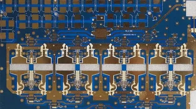
Define what the antenna must accomplish
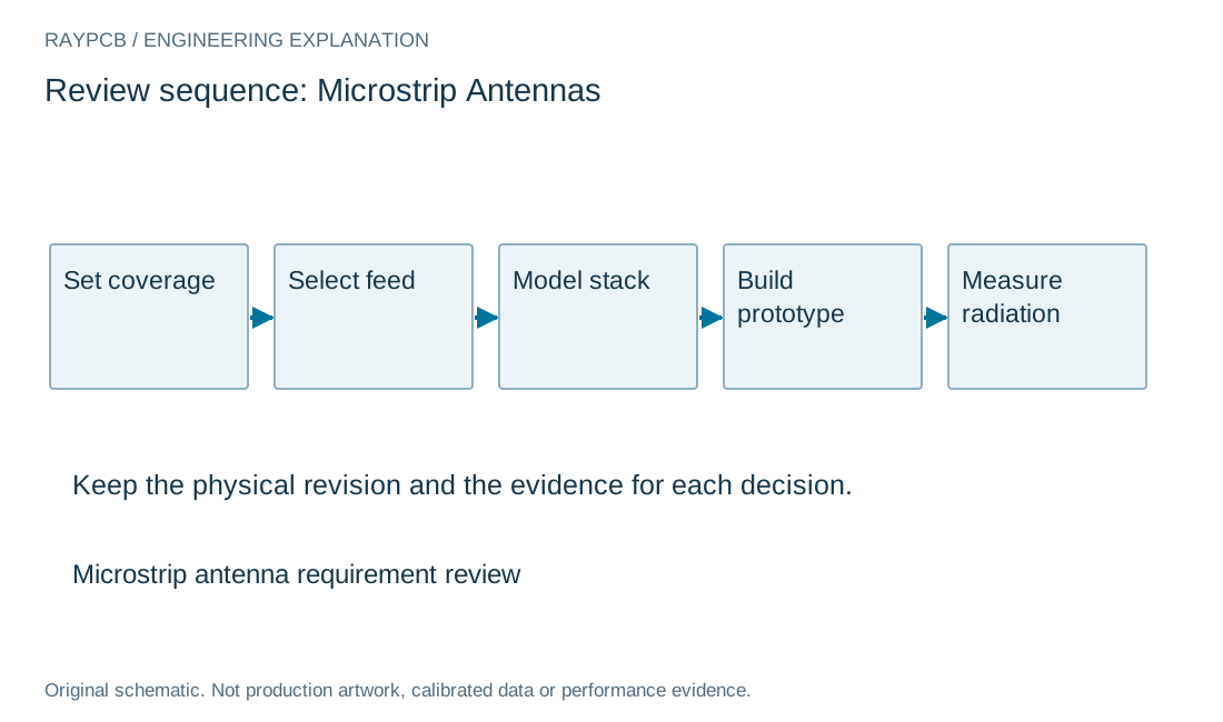
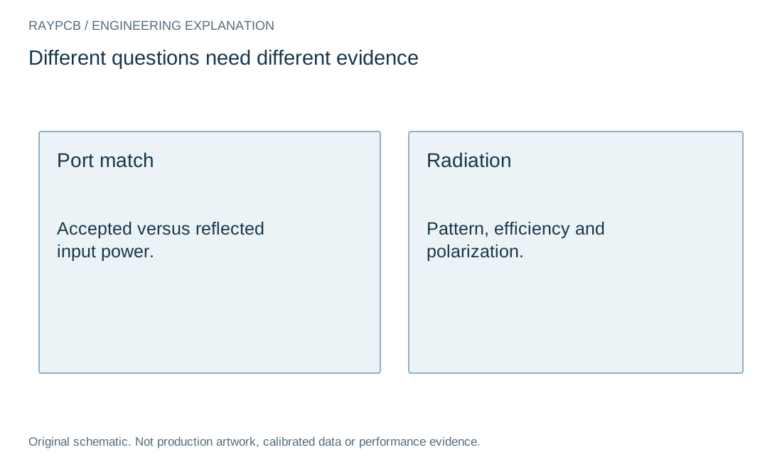
Specify the operating band, polarization, intended coverage, available aperture and profile height. Separate a requirement for input match from a requirement for realized gain or radiation efficiency. A design that is easy to match may not provide the desired pattern, while an efficient radiator can still require a different feed arrangement to meet the port requirement.
Describe the installation. A board mounted against a metal plate, under a radome or beside a display can behave differently from an isolated laboratory sample. Mechanical tolerances and environmental changes belong in the requirement when they influence the antenna. Record which parts of the product are fixed before comparing small geometry adjustments.
For an array, add element spacing, scan requirements, feed-network structure and channel calibration to the task. The isolated element is only one part of the array model. Do not multiply a single-element result by an element count and present the arithmetic as measured array gain. Mutual coupling and the distribution network need their own treatment.
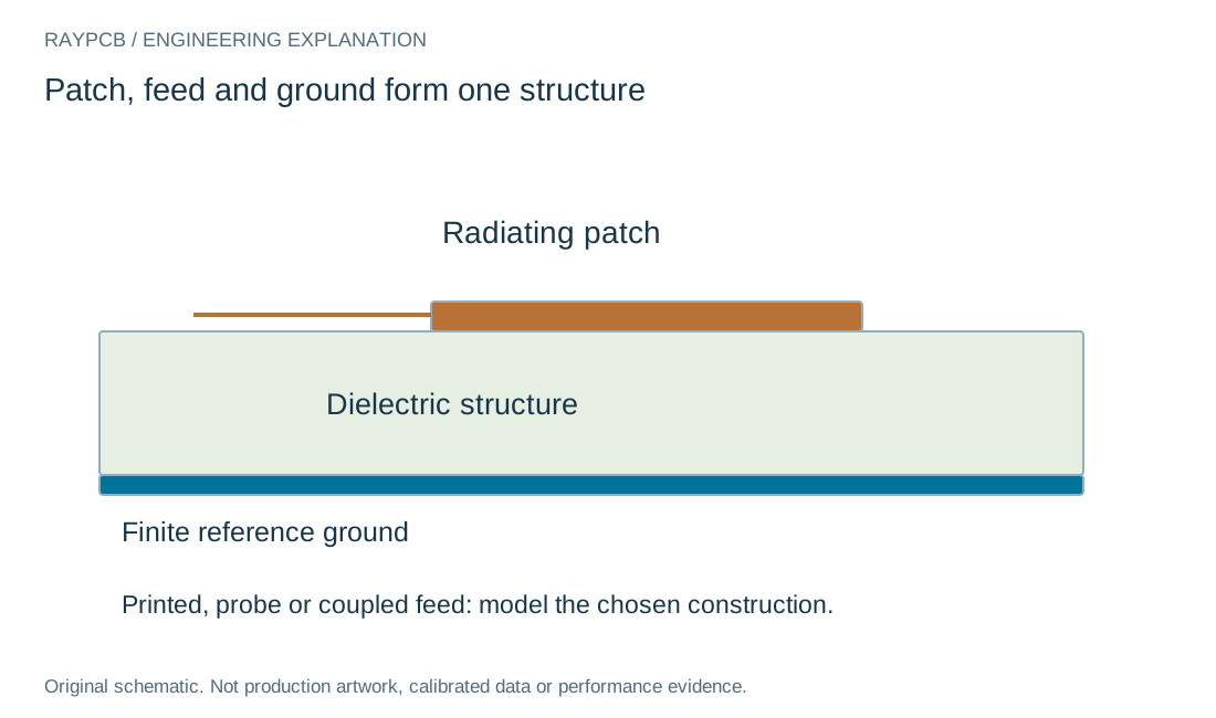
Read the cross-section before selecting the material
Identify the dielectric separation between the radiating conductor and its reference ground. It can be one layer within a thicker multilayer assembly. The thickness printed on a general board quotation may therefore be the wrong value for the antenna model. Keep the exact stack drawing with the RF geometry.
Record the substrate property basis, including frequency, construction and the value used for design. Effective permittivity depends on the field distribution and is not simply another name for material Dk. If a calculator derives effective permittivity from a substrate value, do not feed an already effective value into it without understanding the model.
Copper, coating and nearby structures also matter. A proposed solder mask, protective coating or adhesive can change the electromagnetic environment. Decide which regions are covered and which are excluded, and include those conditions in the prototype. The microwave substrate page connects material choices to transmission and antenna structures rather than listing brands alone.
| Review item | What to establish |
|---|---|
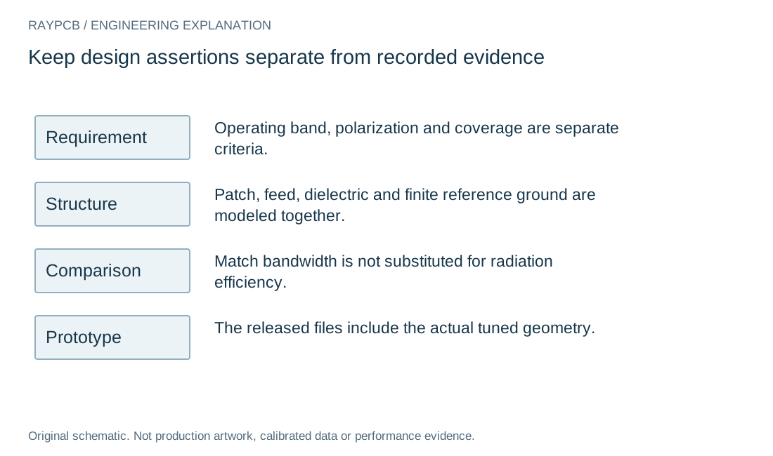
| Requirement | Operating band, polarization and coverage are separate criteria. |
| Structure | Patch, feed, dielectric and finite reference ground are modeled together. |
| Comparison | Match bandwidth is not substituted for radiation efficiency. |
| Prototype | The released files include the actual tuned geometry. |
Microstrip antenna requirement review
Microstrip antenna requirement review
Use the current inputs and keep the assumptions
Enter your own values or use Load example to explore the clearly labeled teaching inputs. The example is not a measured RAYPCB project. Clear for my inputs starts a separate record. Fields identify the units and the physical boundary; missing or unsupported values need correction before a result is generated.
Changing an input invalidates the previous output and disables its download until you generate a new result. A worksheet cannot inspect a board, validate an instrument setup or approve manufacture. Keep its assumptions with any copied number.
Download the current text result if it helps explain a design question. The file stays on your device. Attach or paste it manually when contacting the team; no project information is automatically transferred to the Contact form. Completing this tool is optional.
| Input | What to establish before using it |
|---|---|
| Review reference | Nonconfidential scope or revision. |
| Operating band, polarization and coverage | Choose the evidence state, not an approval. |
| Patch-ground dielectric and copper construction | Choose the evidence state, not an approval. |
| Feed approach and measurement access | Choose the evidence state, not an approval. |
| Finite ground, housing and array boundary | Choose the evidence state, not an approval. |
| EM model, prototype revision and test method | Choose the evidence state, not an approval. |
| Next action / evidence reference | Nonconfidential reference only; no files are inspected. |
Compare feed arrangements by their physical consequences
A printed feed can be convenient to fabricate, but its connection to the patch remains part of the matching problem. An inset, junction or coupled region needs geometry and analysis beyond the nominal impedance of the feed line. Plan measurement access so the feed can be characterized without leaving an unintended stub in the released design.
A probe feed introduces a vertical connection through the structure. Its length, pad and grounding context should be included in the model and assembly drawing. Mechanical convenience does not make the connection electrically invisible. Inspect how the connector or probe is mounted and whether the prototype and intended production arrangement match.
Coupled or aperture-fed structures can offer useful design options but add alignment and multilayer construction questions. Identify which layer defines each aperture or coupling region and how registration is controlled. The best feed choice is the one that meets the electrical and manufacturing task with evidence, not necessarily the one with the fewest visible parts.
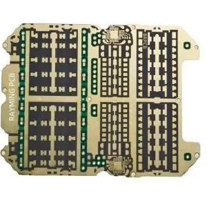
Keep size, bandwidth and loss tradeoffs explicit
Changing substrate height, permittivity or patch geometry changes more than the footprint. Compare alternatives against the required band and installed radiation behavior. A smaller calculated patch should not automatically win if it leaves inadequate tolerance to construction or environmental change.
Loss can make a resonance appear less sharp while reducing useful radiated power. Do not treat a wider match response caused by dissipation as an unconditional antenna improvement. Evaluate the quantities required by the product rather than optimizing a single plot for visual appeal.
Use a controlled comparison matrix. Hold the operating requirement and measurement boundary fixed while varying the feature under investigation. Save the baseline, the changed construction and the reason for the change. If several features must change together, identify the result as a comparison of configurations rather than attributing all improvement to one material property.
Build polarization into the requirement and test
Linear and circular polarization are different system choices, not quality levels. The receiving antenna and propagation environment determine which behavior is useful. For a circularly polarized design, define handedness and the applicable axial-ratio requirement over the relevant band and directions; an input-match result cannot establish those properties.
Record the antenna coordinate system, viewing direction and installation orientation. Ambiguous drawings can make two teams describe the same polarization differently. Include the mechanical mounting datum used during the test so the installed antenna can reproduce the intended orientation.
The L-band patch guide addresses polarization and receiver integration for that application family. It does not assume all L-band antennas are GNSS antennas. Likewise, the 2.4 GHz patch page focuses on required-band coverage and product prototypes rather than repeating a general antenna-type catalogue.
Design a prototype that can answer the unresolved question
Decide whether the first prototype is intended to verify a material model, compare feeds, test a housing effect or demonstrate an installed link. A single board can support several measurements, but each measurement needs a defined boundary. Do not confuse a construction experiment with a completed product qualification.
Preserve calibration information and the actual feed arrangement. If a coaxial cable participates in the environment, keep its routing repeatable. Include mounting hardware and enclosure parts where they affect the task. A good prototype is one whose changes and observations can be explained, not simply the board with the deepest displayed match minimum.
Save raw files and physical modifications. A tuned prototype that was trimmed by hand needs its actual dimensions transferred into the next CAD revision. Record whether matching components are temporary or released. Otherwise the second batch may reproduce the original drawing while the accepted performance belonged to an undocumented version.
Translate the antenna into a manufacturing request
Provide the stackup, critical copper geometry, feed and mounting details, coating instructions and quantity. Distinguish dimensions that are electrically sensitive from ordinary mechanical features. State which supplier adjustments require review and what measurement or coupon evidence is requested.
For an assembled antenna board, include connector orientation, fasteners, soldering details and any tuning operation. A connector substitution can change the launch and mechanical fit even when the mating interface has the same family name. Keep the exact part or a properly evaluated alternative in the BOM.
An early enquiry can still be useful when some parameters are open. Explain whether the goal is a small experiment, an assembled prototype or repeat production. The worksheet records those open requirements and does not issue an automatic feasibility verdict. Use RAYPCB Contact for the actual construction and quotation discussion.
Read a tuning result before releasing the next board
Keep a baseline with a known stackup and installation. Compare a length change separately from a feed change when possible. Save the raw response with the actual physical revision, including any trimming or temporary matching components.
A match improvement and a radiation improvement answer different questions. If the design requirement concerns coverage or efficiency, obtain suitable radiation evidence as well as a port measurement. A well-matched lossy structure can still fail the intended link budget.
Standards, source context and limits
Use the current document for the exact selected component, construction and test method. A vendor application note is not a universal fabrication rule. Agree any applicable acceptance standard and edition for the project; these public references do not certify a board or reproduce licensed acceptance criteria.
Photographs are identified as existing site archive context. They do not establish current factory ownership, calibrated results or a customer's product performance. Original diagrams explain the named engineering boundary and are not production artwork or field-solver output.
For fabrication scope and the agreed construction requirements, see PCB manufacturing.