How to Spot Counterfeit Electronic Components

circuit board electronic components

Introduction

Counterfeit electronic components are a major issue facing the electronics supply chain. Unknowingly using fake or substandard parts can jeopardize product quality, reliability, and safety. Unfortunately, counterfeits have infiltrated authorized distributor channels and even original component manufacturers (OCMs). Combating counterfeits requires diligence across organizations involved in sourcing, procurement, quality control, and production. This article provides guidance on detecting counterfeit electronic components to aid in keeping them out of your supply chain.

How Counterfeits Enter the Supply Chain

To protect against counterfeits, it’s important to understand how they infiltrate the electronics ecosystem. Common paths include:

  • Independent distributors – Unscrupulous brokers re-sell used, recycled, remarked, or outright fake components acquired through various means.
  • Contract manufacturers – Some CM’s cut costs by quietly sourcing from unauthorized channels susceptible to fakes.
  • Online marketplaces – Counterfeiters leverage sites like Alibaba and eBay with little oversight on authenticity.
  • Phony franchises or manufacturers – Imposter operations pose as authorized sources and sell remarketed or fake parts.
  • Recycled materials – Legally recycled e-waste can get unlawfully mixed into new stock.
  • Theft and remarking – Components rejected or scrapped by OCMs get stolen and resold as new.

While motivations and sources vary, the common thread is introducing counterfeit components into supply chains that lack adequate screening processes.

Impacts of Using Fake Components

Xilinx Zynq fpga
Xilinx Zynq fpga

The risks of counterfeit parts include:

  • Product defects – Failure rates may be higher with poor quality or unsuitable components.
  • Safety hazards – Device malfunctions can pose danger to users and the public.
  • Field failures and recalls – Widespread issues upon deployment require expensive corrective actions.
  • Reputation damage – Quality incidents erode customer trust and hurt brand image.
  • Liability – Injury or loss arising from counterfeits can spark litigation.
  • Delays – Discovering fakes during production halts work while sources are reconsidered.

The only sure way to avoid these pitfalls is preventing counterfeits from entering your supply chain in the first place.

How to Detect Potential Counterfeit Parts

Careful inspection, testing, and due diligence is required to reveal signs a component may be counterfeit. Here are key detection practices:

Visual Inspection

Closely examine components for any irregularities compared to the datasheet specifications:

  • Markings – Check for missing, wrong, blurred, or inconsistent labeling
  • Package – Differences in materials, molding, dimensions, weight, etc.
  • Leads – Damage, discoloration, corrosion, or bend/spacing issues
  • Surfaces – Signs of remarking, texturing mismatches, poor plating, etc.

X-Ray Inspection

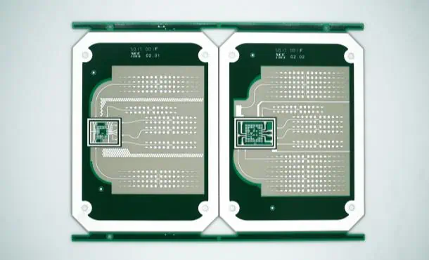
X-ray images reveal internal structures that may deviate from authentic parts:

  • Die size, shape, location, or bond wires don’t match datasheet
  • Missing layers, components, connections, or defects
  • Signs of old die recrystallization from prior use
  • Incorrect substrate, frame, lid, or materials

Electrical Testing

Parameter measurements outside datasheet specs can indicate counterfeiting:

  • Comparative testing of multiple units shows wide variances
  • Functionality testing yields failures
  • Out of spec values for voltage, current, capacitance, frequency, etc.
  • Abnormal waveforms or transient behaviors

Destructive Analysis

Physically delaminating and examining die, packaging, materials, and construction often exposes overt signs of counterfeiting.

Supply Chain History

  • Trace part numbers back through intermediaries to the OCM
  • Verify certifications for each supply chain intermediary
  • Check for continuity and paperwork throughout the chain of custody
  • Look for any high risk entities in the transaction history

How to Avoid Counterfeit Sources

Making sure you only deal with trusted, authorized sources is central to avoiding counterfeits. Here are best practices for qualifying suppliers:

Only Work with Franchised Distributors

Vetted, franchised distributors authorized by the OCM tend to be much more reliable than independent distributors:

  • Verify distributor authorization with the manufacturer
  • Require contractual assurance parts are sourced only from the OCM or other authorized channel partners
  • Get written warranties parts are new, unused, and authentic

Perform Supplier Audits

Conducting periodic audits provides more assurance of supplier authenticity capabilities:

  • Inspect facilities for proper storage, traceability controls, and testing
  • Interview staff on processes for inspector training, sampling, handling defects, etc.
  • Review policies, certifications, record keeping, and quality management
  • Examine inventory for any suspect parts

Require Supplier Certification

Mandatory supplier certification helps screen out disreputable sources:

  • AS6081 – Anti-counterfeiting standard for electronic parts
  • ISO 9001 – International quality management system standard
  • IATF 16949 – Rigorous standard for automotive suppliers
  • Nadcap – Supplier accreditation for aerospace industry
  • AS9100/AS9120 – Standards addressing counterfeit electronic components

Demand Test Reports

Require suppliers provide detailed test reports from independent labs proving parts meet OEM specifications.

Contractual Obligations

Bind suppliers to contracts requiring:

  • Notification if any indication parts may be counterfeit or at risk
  • Certificates of Conformance with accompanying documentation
  • Indemnification against financial damages from supplying fakes
  • Right to conduct unannounced audits of facilities, processes, and inventory
  • Access to traceability and anti-counterfeit records

Anti-Counterfeit Technologies

Some OCMs are adopting emerging tech like blockchain, smart tags, and DNA marking to track, authenticate, and confirm component provenance throughout the supply chain. Require use of these protections whenever possible.

How to Screen for Counterfeits Internally

Xilinx FPGA distributor

Your own inspection processes represent the last line of defense before counterfeits enter production. Best practices include:

Sample Destructive Testing

Perform teardowns, chemical analysis, microscopy, and other destructive tests on a sample of high-risk components to look for counterfeit indicators.

X-Ray Screening

X-ray imaging is very effective at revealing many fake components right away before they get any further.

Thorough Inspection

Use a checklist to methodically examine each aspect of components – markings, dimensions, leads, molding, etc.

Parameter Testing

Test key parameters on a sample of units to identify outliers that merit further investigation.

Random Sampling

Apply screening techniques randomly even across low-risk component batches to keep suppliers honest.

Staff Training

Educate staff on detecting discrepancies that may indicate counterfeiting and flag for further review.

Quarantine Suspect Parts

Isolate any potentially counterfeit parts to avoid them inadvertently entering manufacturing.

Report Issues

Alert internal stakeholders and suppliers regarding suspect parts to trigger further containment actions.

With rigorous prevention and detection controls integrated across the supply chain, companies can effectively combat counterfeits and reduce risk.

Extensive Risk Mitigation for High Reliability Applications

For mission critical systems where failure poses major safety risks, an even higher standard of anti-counterfeiting is warranted:

  • Single, certified source – Restrict component models to a single fuzzy ID/fuzzy factory source under bond.
  • Witness manufacturing – Observe components being made firsthand at the certified supplier.
  • Full traceability – Require unbroken chain of custody with certified handlers from foundry to destination.
  • Destructive lot sample testing – 100% destructive lot sample analyses to validate authenticity.
  • Lifecycle monitoring – Track components while in use with blockchain or smart tag monitoring.
  • X-Ray all parts – Screen every component, not just samples.
  • No exceptions – Refuse any parts where full criteria is not met.
  • Ongoing supplier audits – Conduct exhaustive facility, process, certification, and personnel auditing.

For less critical commercial goods, these measures may be prohibitive. But when lives depend on it, it’s worth the extra diligence and cost.

Conclusion

While counterfeit components continue infiltrating electronics supply chains, taking proper precautions can greatly reduce your organization’s risk. By partnering only with certified, authorized sources, inspecting diligently, and integrating robust counterfeit avoidance practices across procurement, logistics, quality control, and production you can safeguard product integrity. With growing threats from fake parts, enacting comprehensive anti-counterfeiting measures is a wise investment.

Frequently Asked Questions

Q: How extensive of an issue are counterfeit electronic components?

Counterfeit electronic components have grown into a massive issue, with some estimates indicating up to 10% of parts procured from independent distributors are fake. This problem has mushroomed as global supply chains have become more complex. The impact of counterfeit parts can undermine product integrity on a large scale once they enter global distribution channels.

Q: What are some warning signs a supplier may not be trustworthy?

Red flags include reluctance to provide requested documentation like certificates of conformance, audit rights, and test reports. Lack of industry certifications, evasive answers, unusual payment terms, prices that seem too good to be true, vague company ownership, and other shady attributes also warrant further scrutiny of a supplier’s authenticity.

Q: Is it safe to use components purchased from online marketplaces like Alibaba and eBay?

Generally it is risky and not advisable to source electronic components through online marketplaces. These platforms lack oversight to ensure authentic, authorized parts. The prevalence of counterfeits from such marketplaces makes it an unreliable sourcing channel for anything beyond hobbyist or experimental use. For production applications, only trusted franchised sources should be used.

Q: Can visual inspection reliably detect all counterfeit parts?

While valuable, visual inspection alone is not sufficient in many cases. High quality counterfeits may superficially look identical to authentic parts. More advanced techniques like x-ray imaging, sample destructive testing, electrical parameter validation, and supply chain auditing is often required to reliably weed out sophisticated fakes. The right combination of inspection methods and supply chain controls is needed.

Q: What liabilities can arise from using counterfeit electronic components?

Knowingly or negligently sourcing and installing counterfeit parts in shipping products can open companies up to significant legal liabilities. Product liability lawsuits, regulatory fines, and breach of warranty costs can occur if counterfeits cause systems to malfunction, fail prematurely, or result in other damages. It is imperative to demonstrate reasonable efforts were taken to prevent infiltration of fakes.

Farewell to Counterfeit Electronic Components

Everything that is made on earth by humans has a specific life that it works, after that, this product starts to decay or degrade in performance and in the end it may totally collapse or become obsolete. The designers of that product either it be mechanical or electrical takes numerous parameters into consideration to enhance the life time of that product. So these types of electronic items those which have completed their time and become obsolete or have become faulty, or out dated or damaged and become non-repairable will be thrown as โ€œscrap itemsโ€. These scrap electronics is what contributes to e-waste. The business of scrap and e-waste is a very big industry or multibillion dollar industry.

YouTube video

There are countless electronic products that are being scrapped on daily basis throughout the world and this scrap or e-waste is being bought and sold at various prices. Mostly the e-waste or scrap is exported from the USA to China and other countries where it is washed in polluted water of river and then put on sideways to dry up. After that it is then forged by numerous ways like sanding, painting and applying false marks to make it look new. Hence we can say that the biggest source of the counterfeit components is the e-waste or scrap electronic market itself. It is the responsibility of the governments to devise a strategy to properly dispose of e-waste and scrap electronics so that it may not be accessible to โ€œcounterfeitersโ€

What is Counterfeit Electronic Components?

Many of us might have gone through some electronics parts to be used in hobby projects. Letโ€™s say a 555 timer IC is used in an A-stable multi-vibrator circuit. Now the circuit is developed on breadboard and all the wire connections are intact. Power supply is good and you just turned ON your circuit and put oscilloscope at the output of 555 timer IC but you did not get the waveform. You then checked the oscilloscope settings and found perfectly fine. Now you start to think why my output is not coming, because you have blind believe in IC that it has no problem. You are constantly looking errors in your connections, breadboard, oscilloscope and other passive components, then after struggling half or one hour you realize that the IC itself is โ€œcounterfeitโ€ or โ€œfakeโ€. So what happened in the process is the complete waste of your time, money and effort. This what counterfeit components do..!

A counterfeit component is the low quality, faulty and underrated component that is disguised as high quality or new component and it does not perform function correctly or malfunction causing problems for end users or buyers.

Why Counterfeit Electronic Components are made..?

Now that we understand what is counterfeit electronic components and from where mostly they emerge. As for the reason why they exist in markets is the simple reason โ€œMoneyโ€. Yes, it has been estimated that this counterfeit electronic components industry is so huge that semiconductor industry alone was hit by a huge loss of around $75 billion each year. This monetary loss to the genuine semiconductor industrial sector is converted as earnings for โ€œcounterfeitersโ€. But it may be noted that Original Component Manufactures (OCM) have their manufacturing facilities in various countries of the world like China, Singapore, Indonesia and Malaysia. For-example the headquarters of a particular OCM may be in USA but its facilities/factories working in China may develop various levels of quality of a particular component, but they do mention about the quality, performance and also gives guarantees and warranties which is not the case in counterfeit electronic components being sold by โ€œcounterfeitersโ€.

Reason Why We should not use Counterfeit Electronic Components:

As mentioned above by the example of simple 555 timer IC, the main reason why you should avoid using counterfeit electronic components is because it will not work as expected, it will malfunction, it will be a waste of time, your energy and money.  This is with aspect of a student or hobbyist working on a final year project or doing experiments for learning so it may not be a big loss. However if you are an ECM (Electronic Contract Manufacturer) and your production facility has ordered 100,000 pieces of 555 timer IC and out of which 1000 counterfeit then this will be a big issue. The losses are multiplied in terms of every aspect like production cost will increase due to counterfeit components themselves, waste of resources used in production line for example if the components are soldered then whole PCB batch may have to be discarded, the labor cost (hourly wages) of that batch run was wasted, other overhead charges and electricity charges are also counted as loss due to only those counterfeit parts.

Moreover, these above mentioned losses are in the case when the faulty PCB batch (due to counterfeit parts) was caught on right time. But if the production facility members could not catch the problem then the resulting faulty or underrated product will be distributed in market thus annoying the customers and degrading the companyโ€™s (ECMโ€™s) reputation. This will cause lower future orders and customers may lose confidence.

The counterfeit electronic components can damage other electronics parts on the PCB thus rendering the PCB unable or very difficult to repair. The counterfeit electronic components if found in sensitive medical instrument in operation theatre or surgical device can make it stop working randomly thus causing serious issues to human life and can be life threatening. A counterfeit electronic component if found in aircraft electronics can raise serious risk of lives of many passengers and pilot thus these losses are irreversible. This is why medical and aerospace components are always high grade i.e. military spec so there is almost no chance of counterfeit components to get through.

Another reason Counterfeit components should not be used is because they can be dangerous to the overall device or system where they are installed or soldered. Because they can malfunction, or can become short circuit leading to sparking or catching fire or totally damaging the end product/device or even injure the person using it. For example a counterfeit Lithium ion battery can swell and exploded thus injuring the mobile phone user.

Types of Counterfeit Electronic Components:

There is a large number of electronic components sellers, distributors, resellers, wholesalers and manufacturers who deal in electronic components. Majority of them are selling genuine parts but many of them are also among those โ€œCounterfeitersโ€. These counterfeit components are also called forged or fraudulent components that exist in almost every electronics market. Talking about the ECM, it is the responsibility of   supply chain and procurement department to contract very carefully with only those distributors or franchises that are authenticated by OCM (Original Component Manufacturers). It is best to buy components directly from OCM but if not possible then always search for genuine authorized dealers from OCM in your respective country. There are many types of counterfeit components you can encounter. Some of them are

1- Low Specification Components Are Disguised as High Specification Component:

This type of counterfeit component is the one in which a poor quality partโ€™s surface is โ€œsand downโ€ to remove the original markings and then reprint the fake part number to resemble the new high quality component which it is not in actual. Then they polish the surface using thin layer of Blacktopping material.  Sometimes they mix small quantity of low spec parts with large quantity of genuine parts so they cannot be easily identified and sell the whole lot with price of high spec/genuine part per piece.

2- Defective Parts:

As the case above shows the low quality or low grade component are sold by tuning their appearance, here in this case the completely defected component is taken and then same procedure above is repeated and made it look like new part and sold at higher prices. You should be aware of these illegitimate practices of counterfeiters as they can strike a serious dent in your business as discussed above in detail.

3- Used Parts sold as New:

In this case, the used parts are polished and appearance is changed and looks shinier than the genuine part. The problem is that they do not tell their customers that this is used component and it is refurbished but they sell them as new and charge cost of new component which is totally illegal.

How to tell the component is Counterfeit.

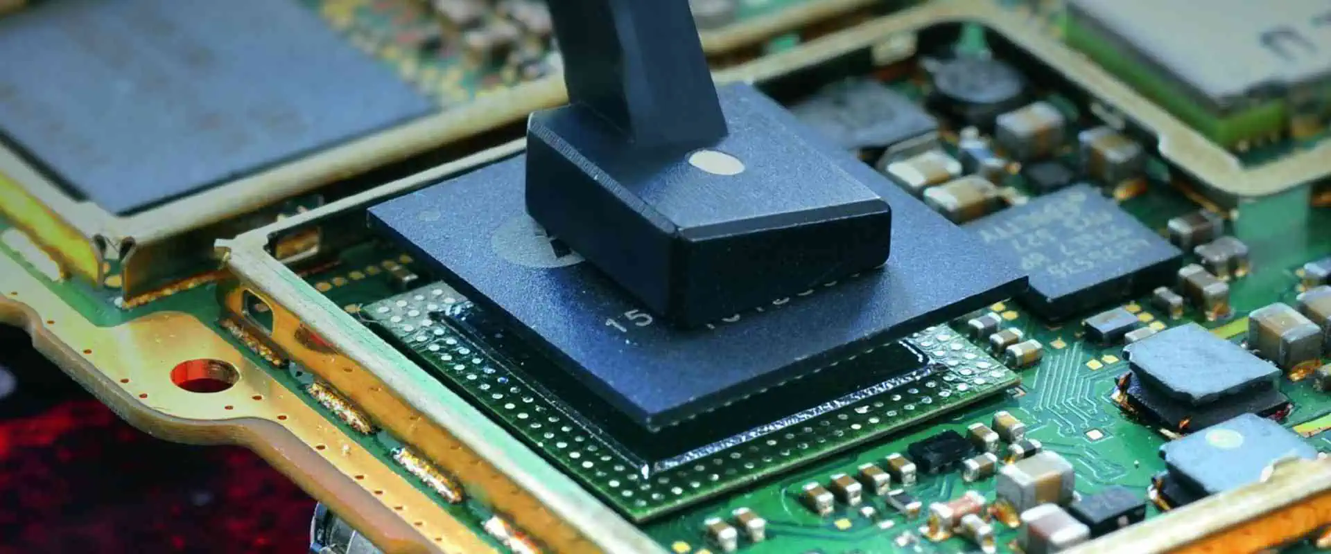
The most important question is how to determine an electronic component to be counterfeit or genuine. In order to do this, you must be an expert or have some experience with electronic components especially with Integrated Circuits. Some basic tools to examine an electronic component are

1- Microscope with high magnification

2- High Definition camera to take pictures then correlate with genuine and counterfeit parts and

3- A solvent like acetone or a solvent that is a mixture of 3 parts spirit and 1 part alcohol in order to remove any fake coatings/markings on the surface of IC.

4- X-Ray machine to examine the inner workings of the IC

5- Electrical testing setup like DMM, Oscilloscope, Function generator and test circuit from Datasheet or Application note.

The common methods to identify a counterfeit component are

1- Check for misspellings and wrong information on labels.

2- Ensure that part number and date coding on the label match those on the part itself.

3- Verify the part number against the genuine part number as OCM uses and ensure it is correct.

4- You can check out for any blunder mistake like date code of the โ€œfutureโ€ labeled on the IC package.

5- Check out for incorrect logo

6- Confirm that the font used on the suspected counterfeit part matches the font used on genuine part.

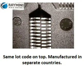
7- Verify the country of origin against the lot code number as the two lots with same code number cannot be manufactured in different countries. So for example if the country of origin name printed on suspected counterfeit part is Malaysia and other genuine part shows Philippines and both parts have same lot code number than it confirms the one is counterfeit part.

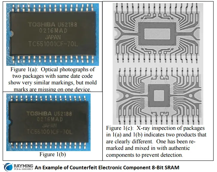
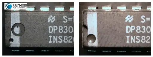
8- Examine the indents. The number one and strongest way to catch the counterfeit component is to examine the indents. Because counterfeiters have a very difficult time keeping the indents clean and consistent during their refinishing process.

For example, in the picture on the right, these two parts were received in the same lot and have identical part number markings. These are the same ends next to each other and you can see that one has 3 indents and the other has just 2. The shape and size of the indents are also different. One is a rounded cavity and the others are all flattened.

Another example of indent is this shown in the figure. The indents from the manufacturer or OCM are always clean and uniform in each and every part of the lot. However this indent shown has been filled up with blacktopping materials that was used to disguise the surface by hiding the old surface.

One more example shows the clear and obvious difference between the two parts having same part number printed from same lot. As shown in figure below the indent on one is much larger and on other it is nonexistent. This is clear and obvious example of counterfeit electronic component.

How to Avoid Counterfeit Electronic Components:

1- Rigorously Control Purchase Sources

2- Always try to buy directly from OCM

3- If not possible to buy from OCM, then go for OCM authorized dealers, suppliers or franchises

4- Look for any reputable distributor who has good reputation and customer feedback if you could not manage points 2 and 3 above

5- Deploy an inspection team that will examine the incoming parts as per the guides hints discussed

6- If you cannot deploy an inception team due to budget constraints then you can outsource the job to third party Company to avoid this headache and speed up the process.

7- Always try to avoid obsolete components in your designs but if unavoidable always look for trusted partner in component sourcing that will not deceive you.

Conclusion:

There are numerous examples of counterfeit electronic components that are floating in the electronic markets. Countless number of sellers, distributers and shops are dealing in these semiconductor electronic ICs, but it is the responsibility of the procurement division of the ECM (Electronic Contract Manufacturer) to rigorously control purchase source and always try to buy directly from OCM (Original Component Manufacturer) or any authorized dealer or franchise of OCM so that the risk of obtaining forged parts is minimized.

How to Generate the Gerber Files

Generate the Gerber Files

Introduction

Gerber files are the industry standard format for printed circuit board (PCB) manufacturing. They provide all the information a PCB manufacturer needs to fabricate your board, including copper layers, solder mask, silkscreen, drill data, and more. As a PCB designer, you’ll need to be able to generate Gerber files from your EDA (electronic design automation) software to send your finished board layout off for production. This comprehensive guide will walk you through the entire process of exporting Gerber files, from understanding the different file types to setting up your layers correctly. With the right preparation, you’ll be able to produce the accurate Gerber files required to turn your design into a physical reality.

The Gerber Format

Gerber files use a standardized numeric format (RS-274X) to convey PCB layout data like images, coordinates, and commands. The files describe each layer of the board layout separately, such as copper, silkscreen, solder mask, drill holes, etc. By separating the data into different files, PCB manufacturers can selectively choose which layers to image during the fabrication process. This eliminates the need to rebuild the entire board layout from a single massive data file.

Some key properties of the Gerber format include:

  • Vector Images – Gerber files use vectors to describe shapes like lines, arcs, and circles that make up tracks and outlines. This makes the format very compact compared to bitmapped images.
  • Apertures – Apertures define the size and shape of the vector. They allow features like pad diameters and track widths to be adjusted by simply changing the aperture.
  • Coordinates – Each vector endpoint is defined by X and Y coordinates that locate features accurately. The coordinates use metric units down to nanometer precision.
  • RS-274X Language – Standardized commands are used for selecting apertures, setting coordinates, interpolating lines/arcs, etc.

By adhering to the standardized RS-274X format, Gerber files can be loaded directly into PCB fabrication equipment without the need for conversion or preprocessing. This avoids errors and keeps the data intact as it moves through the manufacturing process.

Layer Types

Figure 3 Gerber Setup Dialogue Box opens

A fabricated PCB is made up of a number of physical layers that are stacked and bonded together. Gerber files are required to define the data for each individual layer. Here are some of the most common layer types:

Copper Layers

The copper layers contain the conductive tracks, pads, and vias that make up the circuit. There is often a top and bottom copper layer, and also inner layers if using a multilayer board. Each copper layer has its own Gerber file.

Solder Mask Layers

Solder mask is the protective coating that is applied over the copper to prevent solder bridges. The solder mask layers are essentially negative images that define the areas where solder mask should be absent (such as over pads).

Silkscreen Layers

The silkscreen is decorative printing on the PCB. It is used for markings like component designators, logos, board outlines, etc. Silkscreen layers use the Gerber format to define the graphics to be printed.

Drill Files

Drill files specify the locations and sizes of holes to be drilled in the PCB. This includes through-holes for component leads as well as non-plated mechanical holes. Excellon is the most common drill file format.

Assembly Drawings

Assembly files define pick and place data for population of components on the bare PCB. This aids automated assembly and is optional for basic fabrication.

Project Setup Guidelines

Before you can generate proper Gerber files, the PCB project needs to be set up correctly. Here are some key guidelines to follow:

Coordinate System

The coordinate system used should match the PCB manufacturer’s specifications:

  • Origin – Bottom left corner of the board
  • Axes – X horizontal, Y vertical
  • Units – Metric (mm)
  • Rotation – No rotation

This avoids extra processing by the fabricator to align to their system.

Layer Stackup

The layer order and materials should follow the fabricator’s layer stackup convention. A typical example is:

  1. Top Silkscreen
  2. Top Solder Mask
  3. Top Copper
  4. Inner Copper Layers…
  5. Bottom Copper
  6. Bottom Solder Mask
  7. Bottom Silkscreen

Consult your manufacturer’s guidelines and match the sequence in your EDA tool.

Design Rules

Set your track widths, clearances, via sizes, etc. to comply with the fabricator’s design rules for the selected PCB technology. This ensures the layout is manufacturable.

Net Names

Use a consistent naming convention like “GND”, “VCC”, “+5V” for power nets. Avoid changing net names mid-trace as this can confuse fabrication data.

Output Generation

Gerber Files
Gerber Files

Once the project is properly configured, generating the Gerber files is straightforward. Here is the general process:

Cam File Generation

Your EDA tool will have an option to generate cam, photoplot, or fabrication output files from your board layout. Select the appropriate output profile that matches your board technology (e.g. “2 Layer FR-4”). This will generate all required layer Gerber files along with drill, netlist and other fabrication data.

Layer Checking

Thoroughly inspect each layer file to ensure the contents match the source PCB layout. Check for missing traces, incorrect apertures, misaligned layers, etc. Any errors can lead to costly fabrication mistakes.

File Naming

Give the output files clean, consistent names indicating the layer type and order sequence:

  • TopSilkscreen.gbr
  • TopSolderMask.gbr
  • TopCopper.gbr

Avoid using spaces, special characters, and overly long names.

Compressing and Archiving

Zip/archive the complete set of Gerber files together for easier transfer. Avoid compressing individual files as it can confuse CAM systems.

Transferring to Manufacturer

Upload the Gerber archive to the PCB manufacturer through their website portal or send via email. Wait for the files to be checked before proceeding with your order.

Tips for Success

view-gerber-files

Follow these tips to avoid common mistakes and ensure your Gerber files generate accurately:

  • Stay Organized – Keep your PCB layers well structured and named consistently through the design process. Disorganization leads to data mix ups.
  • Follow Standards – Use the manufacturer’s recommended stackup, design rules, and layer settings. Never deviate unless approved.
  • Design Rule Check – Run DRC on your board layout and fix any errors before generating output files. This catches problems early.
  • Double Check Layers – Verify critically that each layer matches your source data. Don’t rely on the CAM process blindly.
  • Communicate Changes – Inform your manufacturer if you need to revise the Gerber files after initial submission. Send the full updated set.
  • Learn from Experience – If you have fabrication issues with your first builds, analyze the cause and improve your Gerber generation process.

Gerber File Viewing and Verification

Since Gerber files contain crucial fabrication data, it is essential to review them carefully for potential problems before sending them out. Here are some tips on how to validate your Gerber files:

Use a Gerber Viewer

A Gerber viewer is specialized software that loads the standard RS-274X files and renders the visual contents for inspection. This provides the most realistic validation of how the manufactured PCB will turn out. Some good free options are GC-Prevue and Gerbv.

Check Layer Alignment

When overlaying layers in a viewer, check that features line up properly across layers. Misalignments lead to etched copper being in the wrong place.

Inspect Apertures and Graphics

Verify apertures are sized correctly and vector graphics render sharply without glitches. Any artifacts could indicate aperture, format, or resolution issues.

Compare vs Source File

Overlay the Gerber layers atop your source PCB data to compare signal-to-signal. Any discrepancies in tracks or pads will show up.

Analyze DRC Reports

Even if your source file passes DRC checks, run DRC on the Gerber files themselves. The CAM process can sometimes introduce new errors.

View Drills & Holes

Inspect drill layers to ensure hole sizes are correct and holes align precisely with pad stackups.

Confirm Critical Data

Double check critical identifiers like designators, component outlines, board dimensions, and text are rendered clearly and without errors.

Thorough Gerber file inspection is the last line of defense against expensive PCB fabrication errors. Spending extra time validating can save you money and headaches down the road.

Converting Gerber to Drill Files

PCB Drilling machine

While Gerber files define the layered 2D data of a PCB layout, drill files specify the actual hole sizes and locations required to fabricate the board. Excellon (.drl) is the standard format for drill data. Here is an overview of how drill files are derived from Gerber:

1. Identify Hole Locations

The locations of all required holes are determined from the component pads and vias defined in the Gerber copper layers. PCB CAM tools extract the X/Y coordinates of every pad/via.

2. Define Hole Sizes

Each pad or via has a associated finished hole size defined during PCB layout. These hole sizes are mapped to the extracted hole locations.

3. Optimize Hole Grouping

To optimize the drilling process, holes are grouped into “tool lists” based on having the same drill bit size. This minimizes tool changes.

4. Generate Excellon File

The formatted Excellon file (.drl) is output containing tool definitions and hole coordinates. The data is organized to facilitate efficient drilling.

5. Add Routing Attributes

Additional routing attributes direct the PCB drilling machine like spindle speeds, tool change positions, and drill cut depths for partially drilled boards.

6. Validate vs Gerber Layers

It is critical to validate the drill file against the source Gerber data to ensure the proper hole sizes and locations transfer over as expected.

With an accurate drill file derived from the layout, the PCB manufacturer can drill all holes to precisely match up with the layered circuit board data.

Advanced Gerber Techniques

For complex PCB projects, additional steps and advanced Gerber techniques may be required:

SolderPaste Files

Solder paste files indicate the precise solder paste distribution required to place and solder surface-mount components. This is often defined as a separate layer.

Removing Explicit Zeroes

Certain CAM systems can misinterpret surplus “zero” command codes. Stripping these out avoids problems.

Simplifying Apertures

Reducing the number of unique apertures in the files helps performance for some fabricators. CAM tools can consolidate apertures.

Polarity Markings

For double-sided boards, adding a small “polarity mark” hole at a standard location aids in orienting and aligning layers.

Routed Tab and Panel Design

Panelization features like tooling tabs, mouse bites, and break-off rails are added for PCB depanelization.

Layer Alignment Markings

Fiducials that appear on multiple layers can provide visual cue points for aligning layers during fabrication.

As you gain experience, continue exploring new Gerber techniques to enhance your fabrication capabilities. The standard allows ample flexibility.

Conclusion

Gerber files are integral to turning your completed PCB layout into a physical board. By understanding the specialized data format, planning your project correctly, thoroughly inspecting your files, and employing advanced techniques, you can generate accurate Gerber files the first time. With clean, error-free data, you will avoid costly delays and re-spins during fabrication. Spending extra time up front to polish your Gerber file creation process ultimately saves you frustration, time, and money further down the line.

Summary of Main Points:

  • Gerber format uses succinct vector data to convey PCB layout information layer-by-layer.
  • Typical layers include copper, solder mask, silkscreen, drill data. Each must have a Gerber file generated.
  • Set up your PCB project according to manufacturer’s guidelines for flawless data output.
  • Carefully inspect all layers for alignment errors or missing data before sending files out.
  • Excellon drill files are derived from copper pad/via locations and holes sizes defined in your layout.
  • Advanced techniques like solder paste layers and panelization require additional data.
  • Take time to refine your Gerber generation process and you’ll produce fabrication-ready files the first time.

Frequently Asked Questions

  1. Why are Gerber files needed for PCB manufacturing?

Gerber files are the standard format that PCB fabrication equipment understands. The files provide the precise layered data needed to image the conductors, solder mask, markings, drill locations, etc. without errors. Trying to fabricate directly from CAD or source layout files would be prone to mistakes.

  1. How accurate are the coordinates in Gerber files?

The Gerber format supports metric coordinates to a precision down to ten nanometers. This allows traces, pads, and holes to be located extremely accurately for high density PCB designs. The precision avoids rounding errors over long distances.

  1. Can you edit Gerber files?

While it is possible to make edits to Gerber files with specialized tools, it is not recommended. The ideal workflow is modifying the source PCB layout, then regenerating clean Gerber output. Direct Gerber edits often lead to conflicts between layers.

  1. What are the main advantages of Gerber X2 format?

Gerber X2 allows greater precision, smaller apertures, step and repeat panelization, embedded component and net properties, and other enhancements. However, adoption of X2 has been slow since traditional RS-274X works well.

  1. How are irregularly shaped traces defined in Gerber files?

Irregular pad/trace geometries are approximated using very short vector segments. Smaller segment lengths increase the precision but also increase file size. There is a tradeoff between accuracy and efficiency.

1.Gerber Files Introduction

Gerber file format is a defacto standard used by PCB manufacturing industry. This is analogous to produce a *.pdf file after designing a graphics or text document. Almost everyone who is involved in PCB design either hobbyist or commercial designer may have used it. It is actually an ASCII file format.

YouTube video

Gerber file format is evolved from applications where it is used to re-create images or graphics i.e., printers and plotters industry. In the same way it is used  in electronics hardware industry to print PCB tracks, holes, clearances and all information which is contained in a *.pcb design file. The leading PCB CAD softwares are able to create gerber files as an output of PCB design file.  These softwares generally use RS-274-X Gerber file format because it is newer and easy to handle data files.

A gerber file is divided into the following four subparts:

  • Configuration Parameters
  • Aperture Definitions
  • Drawing Commands
  • X/Y Coordinates

Each file extension denotes a specific PCB layer such as:

Top Layer => *.gtl

Bottom Layer => *.gbl

Keepout Layer => *.gko

TopOverlay Layer => *.gto

BottomOverlay Layer => *.gbo etc.

2.Generating Gerbers: An example

The softwares have a feature to execute gerber output generate command. Usually, it is a dialogue box which has enable and disable options to include and exclude certain layers and parameters to include or exclude from gerber output files. In RS-274-X file format one file is produced for each one layer of PCB design file.

For instance in protel 99se PCB design software:

The gerber files generator can be launched from (PCB editor) Tools> Generate Gerber files command.

The following CAM Options dialogue box opens:

Figure 1: Setup for Gerber output

However, every software has its own style of creating Gerbers files. They may have small differences compared to others to execute commands. Set of commands that how to generate Gerbers in specific software are best explained in the respective software manual. This example is produced to guide about the process step by step.

The dialog box in Figure 1, produces settings for location to save output gerber files. Almost all PCB designers know to set the folder and file path in a desktop computer.

Figure 2: Gerbers Settings Dialogue Box

The dialogue box in Figure 2, appears to make settings that what to include in the gerber files command, if executed. The first pane makes resolution of scan. The description below to the dialogue box is self-explanatory and can be chosen by clicking the respective radio-box. Higher resolution occupies more memory but have better data precision. There are two settings: the metric (mm) system and imperial (inches) system of units. Gerbers in both formats can be generated. However, for data clarity and to be safe side, generate Gerbers in both mm and inches format, in two separate folders with clearly mentioning their units type.

The next pane in this dialogue box is layers settings where different layers can be enabled to include or exclude in the output files. Generally, it is a good option to โ€œenable all used layersโ€.

Drill drawing and mechanical layers panes make settings about drill drawing and mechanical layers respectively.

Apertures settings is used for thickness of tracks used and advanced is used some other settings. For producing gerber files it is a good practice to consult with your PCB manufacturer.

Figure 3: Settings Dialogue Box for NC drill files

The NC drill files setup produces PCB holes location and drill size information just like the gerber files i.e., location and size of drill. This also has the same settings and parameters as in Gerber files step. Produce the NC Drill files alongwith gerber files.

3.What Should Include In Gerber Files

In a gerber file following layers and information should be added:

  1. Signal layers: All signal layers which are used in the PCB design or those carry electrical signals should be enabled to produce its gerber file.
  2. Plane layers: Similar to signal layers all plane layers should also be enabled to produce gerber output files. These are solid coper layers which distribute power.
  3. Keepout layer: Keepout layer is electrical boundaries of the board. This can also be used to board cutting boundary.
  4. Mechanical layers: The used mechanical layers should also be enabled.  A mechanical layer may not have any electrical information like in signal layer or plane layers. However, they can have some information about mechanical parameter like PCB cutting or fixing in enclosures.
  5. Overlays: The top overlay and bottom overlay which have information of components designators and other PCB nomenclature notes.
  6. Dimensional Information: PCB Dimensions information should be added on top overlay or mechanical or keepout layer of  PCB design file before generating gerber files.
  7. Layer stackup: Before generating gerber files add layer stackup information in any enabled mechanical layers so that manufacturer can use information about PCB material such as base material thickness, pre-preg thickness type etc.
  8. Preferably produce time and date stamped Gerber files so that they would be back traced for any query.
  9. Recheck and verify the file types using any gerber viewer software tool.
  10. If found accurate and forward to the manufacturer.

Figure 4: Gerber files enable and disable and extensions

Figure 4 shows the enable and disable of different layers view in gerber file setup dialogue box .

4.Summary:

The gerber file format is a defacto standard of interface between a PCB Design engineer and manufacturer. Gerber format is RS-274-X 2D ASCII file format. It includes all conductive, mechanical, text and keepout layers information of a PCB design alongwith necessary notes for manufacturing.

The RS-274-X format produces one file for each layer of PCB and is preferred by the PCB industry. It is designerโ€™s responsibility to add layers carefully to generate files. Any confusions and wrong data may cause an surprised and unwanted PCB that may be garbage only.

Applications and Types of PCBs for Automotive Industry

Automotive PCB

Introduction

Printed circuit boards (PCB) play a pivotal role in the functioning and performance of automotive electronics. From powertrain systems to ADAS, infotainment and lighting, PCBs can be found enabling various functions. The harsh under-the-hood environment along with increasing electronics complexity impose stringent requirements on automotive PCBs. In this article, we will take a look at key PCB applications in vehicles, critical design considerations and specialized PCB types used in the automotive industry.

PCB Applications in Automotive

Some major application areas using PCB technology in modern vehicles:

Powertrain Control

  • Engine control unit
  • Transmission control module
  • Battery management system
  • Traction inverter & converter

ADAS Systems

  • Camera modules
  • Radar PCBs
  • LiDAR electronics
  • Vision processing units

Infotainment Head-units

  • Navigation system
  • Audio amplifier
  • Telematics gateway
  • Display graphics module

Body Control

  • Lighting/luminaire PCBs
  • Door control module
  • HVAC control
  • Central gateway ECU

Instrument Clusters

  • Odometer
  • Driver information display
  • Telltales and warning lights

Security Modules

  • Immobilizer PCB
  • Central locking ECU
  • Blind spot detection

PCB Design Challenges in Automotive

Automotive Electronics

Designing PCBs for automotive applications brings unique challenges:

High Vibration/Shock Loads

  • Vibration from engine and road noises.
  • Shock from bumps and unequal road surfaces.

Wide Temperature Range

  • Under-the-hood temperature up to 125ยฐC.
  • Cold temperature down to -40ยฐC.

Electromagnetic Interference

  • Switching noise from motors and actuators.
  • RF interference from transmitters.

High Voltages

  • DC bus voltage upto 650V in electric vehicles.
  • Fast transients like load dump.

Mixed Signal Circuits

  • Combination of sensitive analog and noisy digital circuits.

Safety and Reliability Critical

  • Rigorous product validation needed.
  • Adherence to ISO26262 functional safety standard.

Key PCB Design Considerations

To meet the demanding automotive environment, certain design practices are followed:

Component Selection

  • Automotive grade components rated for extended temperature range.
  • Parts qualified based on AEC-Q101 standard testing.

Layout Design

  • Minimum clearance and creepage distance as per ISO 6469-3.
  • Safety critical layout separation and partitioning.

Power Integrity

  • Robust power distribution network design.
  • Protection against voltage transients.
  • Effective grounding.

Signal Integrity

  • Controlled impedance routing for high-speed buses.
  • Effective EMI and noise filtering.

Thermal Management

Vibration Resistance

  • Component bonding, underfill and encapsulation techniques.
  • Board stiffening elements like aluminum baseplate.

Conformal Coating

  • Paraxylene, acrylic, polyurethane or epoxy coating.
  • Protection against dust, moisture, chemicals.

Safety Standards

  • Compliance to ISO 26262 Functional Safety standard.
  • Adherence to MISRA coding guidelines.

Reliability Testing

  • Industry standard validation as per AEC-Q100, AEC-Q101.
  • Accelerated testing – temperature cycling, humidity, HASS etc.

Types of PCBs Used in Automotive

RF Board for for automotive collision avoidance radar

Different types of PCB technologies and constructions are leveraged to meet the demanding automotive application requirements:

Rigid PCBs

  • Conventional FR-4 glass epoxy rigid PCBs.
  • Higher Tg variants like FR-4 High Temp for thermal reliability.
  • Halogen-free and flame retardant materials.
  • Metal core boards for thermal management.

Flexible PCBs

  • Single, double or multilayer flex circuits.
  • Suit applications with space constraints or movement.
  • Polyimide material for flexibility at higher temperatures.

Rigid-Flex PCBs

  • Combination of rigid and flexible sections.
  • Allows three dimensional routing.
  • Used to interconnect multiple PCBs.

Metal Backed PCBs

  • Insulated metal substrate (IMS) or metal core PCBs.
  • Metal baseplate aids heat dissipation and EMI shielding.

High Frequency PCBs

  • RF designs with precise impedance control and absorbers.
  • Low-loss material substrates like PTFE.
  • Synthetic heat sinks for power amplifiers.

New PCB Trends in Automotive

Emerging trends in automotive PCB technologies include:

HDI PCBs

  • High density interconnects to integrate more functionality.
  • More routing layers, microvias and thinner dielectrics.

High Thermal Conductivity Dielectrics

  • Dielectrics with ceramic fillers for improved thermal dissipation.

Low Temperature Co-fired Ceramic (LTCC)

  • Multilayer ceramic PCBs for demanding RF and power modules.

Additive Processes

  • Additive fabrication to produce high aspect ratio fine features.
  • Technologies like aerosol jet printing.

Embedded Passives

  • Passives like resistors and capacitors integrated within the PCB.
  • Saves space and improves electrical performance.

Panel Level Packaging

  • Panel scale manufacturing vs single PCBs.
  • Allows integration of PCB, ICs, passives etc.

Quality and Reliability Testing

  • Higher reliance on automotive industry standards like AEC-Q100/101, IPC-A-610G Automotive Addendum.
  • In-circuit and functional testing.
  • Accelerated life testing.

Conclusion

From engine control units to ADAS cameras, PCBs have become indispensable in modern vehicles due to the electronics revolution. Automotive PCB design requires mastering signal integrity, robust power distribution, thermal management and mechanical reliability while meeting stringent industry standards. As automotive electronics complexity grows exponentially, innovations in PCB materials, high density integration, quality/reliability validation and panel scale manufacturing will be critical to realize future mobility visions.

FAQs

  1. What are some key factors driving increased electronics content in automobiles?

Demand for connectivity, infotainment, electrification, autonomous features is driving rapid growth in automotive electronics content.

  1. What is the typical temperature rating required for under-the-hood automotive PCBs?

Due to high temperature environment, under-the-hood PCBs must withstand temperatures of 105ยฐC to 125ยฐC.

  1. How does ISO26262 relate to automotive PCB design?

It provides an automotive functional safety framework with requirements traceability impacting PCB design validation.

  1. Which construction provides higher thermal conductivity – IMS or MC PCB?

Insulated metal substrate (IMS) has dielectric directly bonded to metal baseplate giving higher thermal conductivity than metal core PCB.

  1. What are some key board level reliability tests done for automotive PCB qualification?

Common reliability tests include temperature cycling, shock/vibration, humidity/bias, HTOL (high temperature operating life) etc.

The industrial sector has seen a tremendous boom in past decade when the demand in automobile exponentially increased due to rapidly growing automation technology. Today the automobile giants like Toyota, Honda, BMW, Ford and Tesla are producing such a high class automobiles and targeting specific consumer class that can buy such a marvelous piece of art of automation engineering. Besides mechanical engineering miracles we all know that brought the revolution in cars and automobile vehicles, the electronics engineering industry has now got involved extensively in automobile industry. Todayโ€™s automobile vehicle is a combination of true art of mechanical and electronics engineering. All of the aesthetics that we see in high class sports car like Lamborghini or Ferrari, or we see power control system in heavy loaded trucks like Caterpillar or Komatsu lifters, cranes etc we see that the control system working behind is based on some sort of Electronic Control System (ECS). And this ECS is founded on Special kind of Automotive PCB.

Automotive PCB Applications and Types

Applications of Automobile PCBs:

Like Caterpillar 797F mining truck has the electronic clutch pressure control, service break sensor, Engine sensor, ARC switch, service break, secondary break control, axle speed sensor circuit, position and steering sensor circuits. There are lots of other examples of general use consumer cars with impressive dashboard,  with LED or LCD display, GPS and radar electronics embedded on dashboard, FM radio, automatic doors and locking systems, electronic relays to control fuel valves/solenoids, timer circuits for engine, Engine Control Unit (ECU) or Engine Control System (ECS) PCB modules, automatic mirror controller, Airbag controller, and front, rear and side LED light control and drive circuits for headlights, back lights and indicator lights respectively, car speed and acceleration sensor and display circuits, Car Battery Management system circuits, wireless key remote door locking system for car safety, air conditioning control etc.

The auto driver system in modern automobile cars is totally PCB based and highly sophisticated electronic circuits are functioning behind the scene. These PCBs are made pre-programmed for sensing the surrounding environment of car to detect obstacle around it in neat vicinity. This is commonly done by IR and Doppler radar system. The auto robot car driving system will take control of car brake, clutch and race and makes decision based on the inputs from surrounding and programming fed in the complicated automotive PCBs.

Although these automobile PCBs are powered by car batteries which is in most cases maintenance free batteries and all the car electronics is operated by this 12VDC battery system. The cabling and wire harness is laid inside the car along with fuses to prevent the electronics from over current or overvoltage surges.

Automotive PCB Applications and Types

Electric Vehicle:

Nowadays, we see in newspaper, electronic media and people talking about future cars that will run totally on batteries and no fuel or diesel will be required for car now. Yes this is true, scientist and engineers have come-up with a new invention in the battery system that these batteries will charge in the matter of few hours and will give backup to your care for many days. This system is just like our smart-phones that once charged in few hours will give back-up 2-3 days. But there are differences in this novel technology because some electric vehicle will give few days of back and mileage while other can gives battery charging power for weeks. Obviously, the technology of E-Vehicles or Electric Vehicle is not possible without Automotive PCBs. Although our discussion in previous section was just to power up the accessory car electronics and engine control while the fuel was still the diesel and oil, while here in this case the car is totally โ€œelectrifiedโ€ completely eliminating the need of fuel or diesel.

Types of Automotive PCBs:

Automotive PCB Applications and Types

From our discussion above it is clear that the automotive PCBs should be something that will give the highest performance in terms of power dissipation, efficient heat transfer, long life cycle and robustness. Commonly if we open up the deck or dashboard of our cars we see a complex electronics and wiring inside with relays, fuses and sockets mounted and connecting various modules with each other. These Electronic components are all mounted on Rigid PCBs that are High Density Interconnect (HDI) PCBs, Heavy copper PCBs to allow high amount of current flow from car battery to accessory electronic, ceramic substrate PCBs to bear against harsh, stringent environment of car surrounding like car moving in deserts, forest, mountainous regions or running in hot sunny weather.

The aluminum based Metal Core PCBs (MCPCBs) are commonly seen in automotive electronics that consist of bright LED lights. These bright LED lights draw high current from battery and in turn gives high luminosity white light. Moreover the small motors hidden inside car body to control the cars fins, windows, side mirrors or any part that is moving, draws good enough current from battery. Hence the need of heavy copper PCB is required to provide least resistance path to the flow of current so as to protect/avoid PCB to melt down due to high temperature / heat generated by high currents.

There are flexible PCBs also found in car electronics front dashboard, connecting large LED, LCD display to the processor board, or connecting various electronic modules each other by flexible PCBs. Flexible PCBs are light weight and can be adjusted/flexed inside the small space available in car deck/dashboard. The combination of rigid and flexible PCBs called Rigid-Flex PCBs are also found in Automotive PCBs.

Rayming PCB Services for Automotive PCBs:

At Rayming PCB Our expertise in manufacturing automotive PCBs is vast. We assure high quality and robust PCB manufacturing services. Our PCBs are ISO 9001-2008 and UL certified, so you know they are reliable, durable that will last long. We are the one-stop shop for all your PCB manufacturing and assembly needs. Our proven reputation among our valued clients shows the quality product we deliver. Please send us the design specifications and details about your Automotive PCB at this email sales@raypcb.com

Future of Automotive and PCB Industry Together:

These two gigantic industries can change the shape of the automation industry. As we witness today that cars have been invented totally depending upon electricity and batteries and completely knocking out the need of fuel pumps. Now in future electric charging stations will charge your car like a smart-phone and your will then drive your car more โ€œEnergy efficientlyโ€ and more environment friendly. Having said that, the electronics PCB manufacturing and assembly industry is the Part and Parcel of automotive industry. It is just the matter of time that world would see these automotive PCBs being used as an integral part of every carโ€™s engine electronics, as carโ€™s accessories electronics and completely replacing mechanical fuel engines with electronic car engines and interface electric motors to drive your car effectively.

How to Design a Backplane PCB?

impedance control pcb

Introduction

A backplane is a high-speed printed circuit board that acts as the backbone of complex electronic systems like telecom, networking and industrial equipment. It provides interconnections between various cards and modules plugged into the system chassis. Designing reliable and optimized backplanes requires careful planning and execution to meet signal integrity, power delivery and mechanical challenges. This article provides a comprehensive guide on backplane PCB design covering architecture, layout considerations, material selection, analysis and validation steps.

Backplane Basics

Some fundamentals about backplane PCBs:

  • Provides interconnects between various PCBs and hardware units like line cards, switch fabric, storage modules etc. mounted on the chassis.
  • Enables high-speed data transfer and communication between modules using parallel bus interfaces like PCIe, Ethernet etc.
  • Contains multiple high-density board-to-board connectors to plug in cards and daughterboards.
  • Requires very careful impedance control and signal integrity design due to multi-GHz signal speeds.
  • Must handle significant power distribution to provide clean power to all modules.
  • Undergoes thermal and mechanical stresses requiring robust mechanical structure.
  • Fabricated using thick multilayer PCBs with 12+ layers typically.

Backplane Architecture

Defining the right backplane architecture is the first step:

Module Interconnect

  • Analyze inter-module data flow and bandwidth requirements.
  • Select suitable interconnect types like Ethernet, PCIe, proprietary buses etc.
  • Determine number of lanes, data rates, signaling levels etc. for each interface.

Connector Selection

  • Choose right angle or vertical mount connectors based on space availability.
  • Determine mounting type – press-fit, soldered, Z-axis elastomer etc.
  • Select connectors suited for target signal speeds and pin counts required.

Slot Planning

  • Define number and spacing of card slots based on modules.
  • Plan spacing for adequate airflow and cooling.

Form Factor and Dimensions

  • Select suitable backplane dimensions and board outline- ATCA, VME64x, cPCI etc.
  • Define positioning of power connectors, modules, card guides etc.

Electrical Design

Hardware Layout
Hardware Layout

The electrical design focuses on power, signal routing and placements:

Power Distribution

  • Design power tree starting from system power inputs to local regulators on each module.
  • Use thick power/ground planes for distribution of various rail voltages.
  • Add numerous decoupling capacitors adjacent to each connector for clean power.

Layer Stackup

  • Use 20+ layer count stackup with multiple signal-reference plane pairs.
  • Maintain same dielectric materials and thickness throughout for impedance control.

Signal Routing

  • Route critical clock and data lines on inner layers adjacent to reference planes.
  • Match trace widths and clearances to achieve target impedance.
  • Enable impedance control on design software to assist routing.

Component Placement

  • Place bypass capacitors, termination resistors etc. close to connectors.
  • Position on-board controllers, drivers and other active devices optimally.

EMI Control

  • Use shielding gaskets around connectors and board periphery.
  • Include Board-EMI filters for power and signal interfaces.

Mechanical Design

The mechanical design of backplane is also critical:

Card Guides and Support

  • Include guides and slots for precise card insertion and retention.
  • Add stiffeners to prevent board flexing under card weight.

Connector Mounting

  • Use press-fit or soldered connectors to withstand mating cycles.
  • Apply appropriate footprint for selected connector.
  • Add stiff backing supports for connectors to avoid flexing during insertion/removal.

Thermal Management

  • Ensure sufficient air flow channels for cooling.
  • Use thermally conductive dielectric materials.
  • Add thermal pads/vias underneath hot devices.

Vibration and Shock

  • Design robust mounting and retention for mechanical durability.
  • Perform vibration/shock analysis using FEA.

Analysis and Validation

Backplanes require extensive validation due to high complexity:

Signal Integrity Simulations

  • Perform IBIS simulations to evaluate eye diagrams, timing, jitter etc.
  • Analyze signal quality for links like PCIe, Ethernet.

Power Integrity Analysis

  • Execute power integrity analysis focused on AC and transient behavior.
  • Verify power supply regulation, ripple, droop/overshoot are within limits.

Thermal Analysis

  • Carry out thermal modeling using computational fluid dynamics software.
  • Ensure temperature rise is acceptable for devices and dielectric materials.

Prototyping

  • Build multiple prototypes for design validation and testing.
  • Use controlled impedance sockets, loads, probes etc. for evaluation.

Conclusion

Shengyi WLM1 PCB

Designing reliable and high-performance backplane PCBs requires strong foundation in signal integrity, power distribution, electromagnetic compatibility and mechanical engineering. A structured approach covering architectural planning, electrical and mechanical design, prototyping, analysis and testing is key to develop complex backplanes successfully on tight schedules. With growth in data networks and modular systems, role of backplane continues to increase for interconnecting modern electronics systems.

FAQs

  1. What are some examples of standard backplane form factors?

Some common form factors are CompactPCI, VMEbus, FASTBUS, Raceway, ATCA, VXS etc.

  1. How is clock distributed in large backplane designs?

Clocks are distributed through balanced clock trees using traces, striplines and clock buffers for skews control and to minimize distortions.

  1. What are some typical high-speed interfaces used in backplane?

PCI Express, 10Gb Ethernet, Infiniband, RapidIO, StarFabric, Serial ATA are commonly used backplane interfaces.

  1. What type of connectors are suited for backplane applications?

High-density, high-speed board-to-board connectors like mezzanine, HDI and FCBGA types are commonly used on backplanes.

  1. Why are backdrilled vias used extensively in backplane PCBs?

Backdrilling reduces via stubs allowing higher data rates and improved signal integrity for differential traces routed through vias.

Backplane PCBs: Introduction

Generally a Backplane PCB is a collection of multipleconnectors placed and connected on one PCB. By nature its responsibility is to carry signals like a cable from one connector to other but enough good health such as single0ended, differential paired signals, and power supply rails and return paths. The PCBs with semiconductor ICs are directly press-fit over a backplane PCB. These insertable cards or PCBs are called daughter cards. It makes the pins of sourceconnectors to be connected exactly on the required pinsof destination connectors.

YouTube video

A backplane PCB,in complexity is somehow similar to a motherboard PCB in respect of PCB design parameters but it has manydifferences in manufacturing process and functionality. A motherboard, well known to be densely routed signals board with high pin cunt semiconductor ICs. On the other enda backplane is considered an enough connectivity board on the โ€œbackโ€ of boards. But a backplane PCB is much more than a connectivity board especially for high datarate communication systems. A backplane PCB transports allelectrical connectivity of signals and powersin between daughter boards.It also holds and supports daughter cards over it which can be press-fit or extract. 

It increases throughput of system on the cost of increased design and manufacturing effort. Although, the early times backplanes do have wire-wrapped connectorsand sockets but data speed in newer systems has realized to utilize advance PCBs materials and manufacturing skills for backplane PCBs. It originated further PCB manufacturing constraints alongwith the existing ones. PC (Printed Circuit) based Backplanes are preferred over wire-wrapped backplanes due to their increased reliability and data carriage capability.In common practice Backplanes donโ€™tcomprises of semiconductor chips over them. However, they have small electronic components like resistors, capacitors, filters and chassis ground circuitry over them.

Backplane Manufacturing Difficulties:

The Backplane PCBs have enhanced data throughput, signal travelling quality, ease of assembly and production but still it increased challenges for PCB manufacturers.

The Backplane PCB thickness increases because it consists of several high speed controlled impedance transmission lines, supply rail planes ad return paths.Transmission of high frequency data over longer traces requires wide signals traces to reduce signal attenuations.  It needs thicker dielectric capable to maintain impedance and keep the signal absorption lowest. Increasing trace width decreases signal density in a layer in per unit area of PCB. On the other hand increasing dielectric thickness increases overall PCB thickness.

Insertion of more signal layers added to power planes and return planes increases layer count that finally approaches to 20 or even more.It becomes challenging to maintain standard thickness of PCB for a manufacturer with given materials and impedance matching parameters.

High speed fine PCB drilling for vias and connectors in backplanes works well till a thickness of 5 to 6mm. However, larger drill diameters are required for thicker PCBs. Higher drill aspect ratios such as 8:1 constraints manufacturer to volumetric production so thicker PCBs require multiple drill passes for a single via.

It is a common practice to through daughter cared input power supplies by backplanes for examples ยฑ5V, ยฑ12V and ยฑ24V DC. Many a times each power rail needs a separate return path plane to reduce PCB commotion. In such a way it may need upto 12-layers for power supplies.Framework computers having high current power supplies which produce IR losses over the planes copper. Thatneedsheat sinks or heat radiator fans for temperature compensation. Their leading layers need thicker copper compared to other internal layers.With higher layer count PCB layer registration, via alignment, pad-hole alignment and pressing a thicker PCB also becomes difficult.

Overall a high-speed backplane PCB increases entire manufacturing process through routing complexity, etching, layer registration, thickness, weight, material selection, and cost and production process.

  • PCB Pressing

In thicker backplanes manufacturing drilling becomes more complicated. A lengthy drill hole requires multiple times drilling the hole. It decreases drilling accuracy ad PCB yield percentage. It degrades high frequency performance.

  • High density etching

In a backplane PCB due to high count of connectors so their mounting holes and pads use significant part of PCB real-estate. The PCB designers strive to increase signal routing density maintaining impedance, trace length, instead of increasing number of layers. The increased signals density increases etching complexity. It pushes the trace, via-hole, pad-hole, annular ring geometries to the fabrication tolerance limits.

  • Impedance matching

With high speed data transmissions in the backplane PCBs impedance matched PCB fabrication becomes a challenge.Data transmission in GB per second range is generally not recommended over general FR-4 materials. The dielectric constant and dissipation factor dictate the material selection for backplane PCBs. This creates a challenge for PCB manufacturer to provide PCBs on demanded materials. The transmission line impedance, via impedance and connector pad to pin impedance also becomes a challenge. A new material type needs PCB manufacturing process to be slightly amendedat manufacturer facility.

  • Via back-drilling

As unused copper piece in PCB can act as stub in high frequency signals.The similar stub-effect may occur due to unused via barrel copper and annular ring. For this purpose PCB manufacturers are pushed to back-drill PCB. It requiresremoving the redundant via barrel from a thru-hole via in a PCB.  The manufacturer removes thatvia copper after PCB fabrication is complete byre-drilling the target holes with a different drill size, leaving a certain length after last layer connection. It slows the production and causes inaccuracies in PCBs.

  • Connectors Alignment

A high speed backplane has good impedance matched connectors over it.  In general a backplane has around 50 impedance controlled differential pairs per square inch. So the total differential pair length approaches to 500 pairs in a plane.The high density SMD and through-hole connectors allow smaller PCB size but they need many blind press-fit insertion and extraction of daughter cards from it. It harmsdurability of PCB. The manufacturerconstraint arises to maintain a hole-locations and geometry of connectors as well as maintaining the signal integrity throughout the PCB.

  • Layer registration

Layer registration in high speed high density PCBs causes low accuracy during copper etching, lamination, drilling and dimensional stability. The signal integrity and PCB yield at smaller sizes becomes more challenging for manufacturer.

  • Aspect Ratio

Aspect ratio is the ratio of drill size to PCB thickness. Dense signals routing,higher copper layers count, and high vias and connector through-holes count in a backplane makes itsaspect ratio high that leads manufacturingdifficulties.PCB design engineers strive to maintain an acceptable ratio figure effective for PCB assembly china and durability. Manufacturers are pushedto manufacture PCBs with 10:1 aspect ratio. However, 6:1 aspect ratio is a common number.

Other common problems which are related to backplane PCBs manufacturing of backplane PCBs are CAF (copper anodic filament), impractical stackups (such as odd-numbered layers PCB design), thickness control of multilayer PCB and high-pressure compression, incomplete manufacturing information, incorrect blind and buried vias placement, improper layer-pairs, environmental impacts on PCB core and pre-preg materials, stringentrequirementsforced by international body regulations.

What is PCB Electroplating ?

ENEPIG pcb

Introduction

Electroplating is a key process used during the manufacturing of printed circuit boards (PCB) to deposit metallic coatings on the substrate. It involves electrodeposition of a thin film of metal like copper, tin, nickel, gold etc. onto the PCB to build up the conductive traces and interconnects. In this article, we will learn the basics of electroplating and its role in PCB fabrication.

Why Electroplating is Used in PCBs?

Electroplating provides the following benefits for PCB manufacturing:

  • Enables depositing uniform, smooth and dense metal coatings.
  • Allows building up PCB copper thickness up to 1 oz/ft2 or higher.
  • Deposits can be precisely controlled by process parameters.
  • Conformal step coverage into small openings and vias.
  • Cost-effective process with high throughput.
  • Suitable for plating a wide range of metals like Cu, Sn, Ni, Au etc.
  • Environmentally cleaner compared to many coating processes.

Thus, electroplating is ideally suited for metallization of PCBs during fabrication.

Electroplating Process Basics

PCB pattern plating line

Electroplating involves applying a voltage between two electrodes immersed in a salt solution (electrolyte) to drive metal deposition onto the cathode surface.

Key Components

  • Anode – Positive electrode providing metal ions into the solution. Made of the metal being plated.
  • Cathode – Negative electrode to be plated. The PCB acts as the cathode.
  • Electrolyte – Contains aqueous solution of metal salts and other additives.
  • Power Supply – Applies direct current between electrodes.

Basic electroplating process setup showing anode, cathode, electrolyte and power supply.

Mechanism

When a DC voltage is applied, the metal atoms of the anode dissolve into the electrolyte as positive ions.

The PCB substrate acting as cathode is charged negatively. This attracts the positively charged metal ions in the electrolyte to deposit onto the PCB surfaces forming a thin metal coating.

Electroplating in PCB Fabrication

Electroplating is utilized at multiple stages during the manufacture of a printed circuit board:

1. Copper Electroplating

  • After drilling and desmear, copper is electroplated to build up traces on the PCB.
  • Multiple plating cycles with increasing thickness are used to reach final copper thickness.
  • Plating rates up to 1 mil/min can be achieved.

2. Tin-Lead or Tin Electroplating

  • Tin-lead or pure tin plating applied on surface pads for solderability.
  • Provides good solderability for SMT component assembly.

3. Nickel and Gold Plating

4. Via Hole Plating

  • Copper is electroplated to build up metallization inside drilled via holes.
  • Ensures electrical connectivity between layers.

5. Electroless Plating

  • Used before electroplating to deposit initial conductive layer on dielectric surface.
  • Provides base for subsequent electroplating.

PCB Electroplating Process Steps

The PCB electroplating process involves the following key steps:

1. Cleaning

  • PCBs are thoroughly cleaned to remove oils, dust particles and debris from surfaces.
  • Hot alkaline cleaning agents are commonly used.

2. Microetching

  • Microetching done using chemical or plasma etching.
  • Removes surface contaminants and oxidized copper.
  • Creates microscopic roughness to improve adhesion.

3. Electroless Plating

  • Electroless copper plating applied first to make PCB surface conductive.
  • Between 0.1 to 0.5 mil thickness plated.
  • Provides base layer for electroplating to build upon.

4. Photoresist Coating

  • Dry film or liquid photoresist coated on PCB surfaces.
  • Photolithography used to create plating resist pattern.

5. Electroplating

  • PCB connected as cathode and immersed in electrolytic bath.
  • Desired metal deposited using DC current for required time.
  • Plated metal thickness increases with plating time.

6. Resist Stripping

  • Photoresist stripped away revealing conductive pattern.
  • Typically removed using chemical stripping process.

This completes the PCB electroplating process. The boards may go through additional plating processes to deposit tin, nickel, gold etc.

Electroplating Process Parameters

The key process parameters that determine the electroplating results:

  • Current Density – Controls plating rate. Typical range is 20 to 120 A/dm2. Higher current densities increase plating speed.
  • Voltage – Typical plating voltages around 3-9 V. Higher voltages improve throwing power.
  • Temperature – Typical range of 20-30ยฐC. Higher temperature increases plating rate.
  • Agitation – Solution movement using pumps or agitators improves deposit uniformity.
  • Additives – Additives like brighteners refine the grain structure and brightness.
  • Time – Plating time controls metal thickness. Time is adjusted to achieve target thickness.

Advantages of Electroplating

Some benefits of using electroplating for PCB fabrication:

  • Produces uniform metal coatings with good dimensional control.
  • Allows building up of copper thickness to over 1 oz.
  • Recesses and vias can be covered through optimal throwing power.
  • Reduces porosity in the metal deposit.
  • Operates at close to room temperatures.
  • Provides high production rate and throughput.
  • Lower cost compared to some physical vapor deposition techniques.
  • Simpler equipment and setup compared to CVD, PVD.
  • Allows depositing a wide range of metals.

Limitations of Electroplating

Some limitations of electroplating include:

  • Metal purity is lower compared to vapor deposition techniques.
  • Plating thickness inside openings falls as aspect ratio increases.
  • Requires additional processing steps for resist patterning.
  • Stripping and cleaning steps produce liquid effluents.
  • Corrosion and maintenance requirements of electrolyte bath and anodes.
  • Metals like aluminum cannot be electroplated.
  • Difficulty plating non-conductive substrates without seed layer.

Conclusion

Electroplating is an efficient and cost-effective process that enables metallization of printed circuit boards during fabrication. It allows depositing a wide range of metals like copper, tin, nickel to build the conductive traces and interconnects on the PCB substrate. By selecting optimal process parameters and electrolyte composition, electroplating provides an ideal solution for metallization of PCBs in a high volume manufacturing environment.

FAQs

  1. How is electrolytic copper different from electroless copper plating?

Electrolytic copper requires applying external current while electroless copper relies on auto-catalytic chemical process without external power.

  1. What are some surface finishes deposited by electroplating on PCBs?

Common PCB surface finishes plated include tin, tin-lead, nickel, gold, silver and palladium-nickel coatings.

  1. What defects can occur during electroplating?

Burning, pitting, nodulation, cracking, peeling, contamination, over/under-plating are some common electroplating defects.

  1. Why is pattern plating done for PCB fabrication?

Pattern plating allows selective electroplating only in desired conductor pattern. This eliminates need to etch away unwanted copper after plating.

  1. What are auxiliary anodes used for in PCB electroplating?

Auxiliary anodes placed near edges/corners compensate for low current densities in those areas and enable more uniform plating thickness.

What is Package on Package (POP) Assembly ?

package on package assembly

Introduction

Package on Package (POP) is an integrated circuit packaging technique used in electronics manufacturing where packaged semiconductor devices are stacked vertically using solder balls. This enables higher component density and improves electrical performance for advanced PCB designs. In this article, we will explore the fundamentals of POP technology, its assembly process, advantages, limitations, applications and future trends.

Overview of POP

POP involves integrating two or more completely packaged devices into a single composite component unit by stacking them vertically. Some key points:

  • Each device is separately packaged first before POP assembly.
  • Devices are interconnected using solder balls or bumps.
  • The bottom device is called the โ€˜base packageโ€™.
  • The top stacked package is called the โ€˜top packageโ€™.
  • Interposer may be used between packages for re-routing.
  • Entire POP assembly is treated as a single packaged component.
  • Also referred to as package-on-package (PoP) or package-over-package.

POP configuration showing stacked packages interconnected by solder balls.

Why POP is Used?

Some key benefits driving the adoption of POP technology:

  • Allows vertical stacking of ICs for increased component density on PCB.
  • Enables integrating disparate technologies like memory, processors, sensors etc.
  • Improves electrical performance through double-sided interconnections.
  • Provides flexibility for modular designs by stacking known good packaged devices.
  • Simplifies PCB routing by reducing number of components required on board.
  • Allows customized configurations suited for target application.
  • Reduces the overall footprint and height compared to side-by-side placement.

POP Components

https://www.youtube.com/watch?v=ECBTjZPoki8&t=32s

POP assembly combines two main types of packaged components:

1. Base Package

  • Typically contains high pin count device like application processor.
  • Provides mechanical support for POP structure.
  • Made with standard packages like FBGA, PBGA, LGA etc.
  • Contains high density of solder balls or bumps on top side.

2. Top Package

  • Usually a memory device like DRAM, flash etc.
  • Comes in packages like TSOP, CSP or wafer-level CSP (WLCSP).
  • Has solder balls only on bottom side.
  • Smaller in size than base package.

Interposer

  • Optional substrate placed between base and top package.
  • Facilitates re-routing of I/O connections.
  • Used to optimize pad layout or enable high density ball grid array (BGA).

POP Manufacturing Process

POP assembly involves the following key manufacturing stages:

1. Sourcing Packaged Components

  • Obtain fully packaged and tested base and top devices.
  • Components must be compatible for stacking and interconnections.

2. Applying Solder Paste

  • Dispense solder paste on base package substrates using stencil.
  • For some assemblies, paste may also be applied on top package.

3. Placing Base Package

  • Mount base package on PCB using standard SMT process.
  • May involve reflow soldering to secure base package.

4. Attaching Top Package

  • Position top package accurately over base package.
  • Orient top package solder balls with base package pads.

5. POP Reflow

  • Reflow solder entire POP assembly to form solder joints.
  • Special oven profiles are used to manage thermal stresses.

6. Underfill Dispensing

  • Wick underfill material via capillary action to fill gap between packages.
  • Underfill provides mechanical stability and prevents stress on joints.

7. Conformal Coating

  • Apply protective encapsulating material over entire assembly.
  • Improves reliability and environmental resistance.

This completes the POP manufacturing process. The components are then put through inspection, programming, testing etc. based on specific product requirements.

POP Design Considerations

Some POP design factors to consider during PCB layout and assembly process planning:

Package Selection

  • Height of stacked packages to meet overall height constraints.
  • Compatible ball pitch, materials and CTE between packages.
  • Solder ball alloy suited to reflow process.
  • Underfill fill requirements based on gap between packages.

Electrical Design

  • Electrical connectivity through solder balls between packages.
  • Minimal stubs lengths for signal routing.
  • Matched impedances for high speed signals.
  • Power, ground and thermal management.

PCB Land Pattern Design

  • Pad shape and size to suit BGA packages.
  • Sufficient clearance between pads and surrounding tracks/vias.
  • Non-solder mask defined pads.

Solder Paste Stencil Design

  • Stencil thickness, aperture size, shape for optimum paste release.
  • Step down thickness in stencil for base package pads.

Process Considerations

  • Compatible reflow profile to solder both packages.
  • Underfill dispensing process window.
  • Balanced placement to minimize warpage.

Advantages of POP

The major benefits provided by Package on Package technology are:

Increased Density

  • Stacking components vertically conserves PCB area.
  • Reduces length of interconnects between packages.

Enhanced Electrical Performance

  • Double-sided interconnects minimize parasitic inductances.
  • Wider power/ground connections improve current delivery.

Lower Height Profile

  • POP provides about 60% height reduction compared to side-by-side placement.
  • Lower profile critical for thin and compact product designs.

Design Flexibility

  • Allows integration of disparate package types.
  • Custom configurations possible by mixing components.

Improved Manufacturability

Cost Savings

  • Eliminates SiP substrate, interconnect layers.
  • Shared reflow process reduces costs.

Disadvantages and Limitations

Some drawbacks and challenges of using POP approach:

Thermo-mechanical Stresses

  • CTE mismatch between packages induces stresses during thermal cycling.
  • Can affect long term reliability of solder joints.

Narrow Process Window

  • Reflow profile optimization is critical for good joint formation.
  • Underfill voiding can occur due to improper dispense process.

Warpage Control

  • Unbalanced stacking leads to significant warpage.
  • Requires symmetrical design and placement during assembly.

Design Constraints

  • Restricts pin assignments, placement and routing on PCB.
  • Requires extensive modeling and analysis.

Inspectability

  • X-ray inspection capability needed to detect defects under top package.
  • Fault isolation challenging in stacked configuration.

POP Applications

Some common application areas where POP technology provides benefits:

Smartphones

  • Memory+processor stacking enables powerful smartphones.
  • Allows integrating memory, power management, RF and sensors.

Wearable Devices

  • Miniaturization for compact wearable product form factors.
  • Lightweight flexible POP solutions ideal for wearables.

Internet of Things (IoT)

  • Small footprint and height critical for many IoT devices.
  • Custom stacking combinations possible for specific devices.

High Density Interconnects

  • Doubled interconnections density compared to peripheral arrays.
  • Well suited for processors requiring high bandwidth memory.

Automotive Electronics

  • Rugged POP packages able to withstand temperature cycling.
  • Suitable for engine control units and in-vehicle infotainment.

The Future of POP

Some emerging trends and developments in POP packaging technology:

  • Hybrid POP configurations integrating passives, sensors along with active ICs using fan-out wafer level packaging.
  • Development of ultra-thin wafer level CSPs as top package for slimmer POP.
  • Utilization of 2.5D and 3D silicon interposers with fine-pitch interconnects.
  • Adoption of through mold vias (TMV) for signal and power delivery through package substrate.
  • Flip-chip underfill process improvements to enable ultra-fine pitch POP scaling.
  • Novel conductive adhesives like anisotropic conductive films (ACF) as interconnect material.
  • Wafer-on-Wafer (WoW) integration for direct device-to-device fine pitch interconnections.
  • Applications in high performance computing and networking equipment.

Conclusion

Package-on-Package represents an exciting packaging innovation that enables continued miniaturization and performance scaling of electronic systems through vertical stacking. With its advantages in density, electrical performance and design flexibility, POP will continue to find increased applicability in space-constrained mobile devices, wearables, IoT as well as high performance designs. Ongoing research and developments are focused on pushing the limits further in terms of interconnect density, stack height, thermal management and manufacturability. As semiconductor integration advances, POP promises to provide an ideal platform for heterogeneous integration of multiple dies and components.

FAQs

  1. How is POP different from package in package (PiP) approach?

In POP, electronic packages are stacked one over the other. In PiP, one package is placed inside another larger package before interconnecting.

  1. What interconnect materials can be used for POP assembly?

Besides solder balls, conductive adhesives like anisotropic conductive films (ACF) and anisotropic conductive pastes (ACP) are also suitable POP interconnects.

  1. Does POP eliminate the need for SiP and multichip modules?

POP provides an alternative by directly stacking known good pre-packaged components. However, SiP and MCM are still used when custom or incompatible devices need to be integrated.

  1. What causes warpage in POP assembly and how is it controlled?

Unbalanced thermal expansion between differently sized top and bottom packages induces warpage. Careful package selection, symmetrical placement and substrate stiffening help reduce warpage.

  1. How does thermal management differ for POP compared to conventional PCB assembly?

Concentrated heat density requires effective heat spreading to packages. Thermal vias, large ground pads and heat slugs are commonly used techniques.

How to Export Gerber Files from Eagle

eagle pcb design

Introduction

EAGLE (Easily Applicable Graphical Layout Editor) is a popular PCB design software used by engineers, hobbyists and students. It provides a seamless workflow from schematic capture to PCB layout and includes powerful features for generating manufacturing files. This article provides a comprehensive guide on exporting Gerber files from an EAGLE PCB project.

Overview of Gerber Files

Gerber files are the industry standard for transferring PCB design data to fabrication and assembly units. Here are some key facts about Gerber files:

  • Contain vector image data of PCB layers like copper, mask, silkscreen, drill files etc.
  • Use RS-274X file format with .gbr extension.
  • Provide image plots of fabrication layers for photoploting.
  • Required by PCB manufacturer along with drill files to manufacture the board.
  • EAGLE uses extended Gerber format RS-274X with additional features.

CAM Processor Settings

Before generating Gerber files, the CAM processor settings must be configured in EAGLE to specify file outputs. This is done through the CAM editor.

The important CAM job settings are:

  • File Format โ€“ Extended Gerber RS-274X.
  • Coordinates โ€“ Absolute or Incremental depending on manufacturer requirements.
  • Leading and trailing zeros โ€“ For consistent file formatting.

-asymperc Output directory โ€“ Location to save output files.

  • File naming convention โ€“ Unique names for identification.
  • Layer mapping โ€“ Links board layers to Gerber files.
  • Additional outputs โ€“ Like drill files, drawings etc.

Properly setting up the CAM job is essential for clean and error-free Gerber generation.

Generating Gerber Files

schematic-eagle

Once the CAM processor settings are configured, we are ready to export the Gerber files. The steps are outlined below:

  1. Open the PCB project in EAGLE.
  2. Run the Design Rule Check to ensure the layout passes all checks.
  3. Open the CAM processor window from the File menu.
  4. Select the configured CAM job and click on the Process Job button.
  5. Specify an output directory when prompted.
  6. Review the final summary and click on OK.
  7. The Gerber files are generated in the defined output folder location.
  8. Additionally, a job report is created detailing file outputs.

This completes the generation of fabrication-ready Gerber files along with drill, mask and other layers as specified in the CAM job.

Layer Mapping

A key aspect of the CAM job settings is mapping the PCB layers correctly to the desired Gerber files. The typical layer mapping is:

PCB LayerGerber File
Top Coppergt[name].gbr
Bottom Coppergb[name].gbr
Padsgp[name].gbr
Viasgv[name].gbr
Top Soldermaskgts[name].gbr
Bottom Soldermaskgbs[name].gbr
Top Silkscreengto[name].gbr
Bottom Silkscreengbo[name].gbr
Board Outlinegko[name].gbr
Drill Holes[name].xln / [name].drd

where [name] is the file name prefix. Additional inner layers are mapped similarly.

Important File Outputs

Some of the key Gerber files needed for PCB fabrication are:

  • Top and Bottom Copper Layers โ€“ Contain signals and traces.
  • Solder Mask Layers โ€“ Define solderable areas on the PCB.
  • Silkscreen Layers โ€“ Include component designators, values, logos etc.
  • Drill Files โ€“ For creating NC drill machine program.
  • Board Outline โ€“ Dimensions of final PCB profile.
  • Inner Layers โ€“ Used for multilayer boards.
  • Assembly Drawings โ€“ Help guide component placement.

File Generation Tips

Here are some useful tips to generate clean Gerber files from EAGLE:

  • Always run DRC and ERC checks before generating Gerbers to avoid errors.
  • Ensure all design data is on specified layers to be correctly output.
  • Confirm board outline is closed polygon without gaps or missing segments.
  • Use unique and intuitive names for file identification.
  • Enable zipping of output files for compressed transfer.
  • Specify consistent number of decimal places for file formatting.
  • Round hole sizes to match manufacturer drill sizes to avoid errors.

File Validation

Before releasing Gerber files for fabrication, they should be thoroughly validated:

  • Visually inspect files in a Gerber viewer to ensure proper images.
  • Use pre-flight tools to verify file format, apertures, parameters etc.
  • Get test film photoplots made from files to validate accuracy.
  • Compare the images with board layout to catch any missing data.
  • Confirm critical clearances are maintained in files through measurement.
  • Check if generated drill file matches holes designed in PCB.

Thorough file validation prevents costly errors from propagating to manufacturing stage.

Panelization

For assembly of multiple PCBs, the boards need to be arranged in a panel to optimize manufacturing. Steps:

  1. Create the required panel layout by arranging board outlines.
  2. Generate a new Gerber file containing just the panel outline.
  3. Modify main board outline file to remove outline.
  4. Include the panel file along with other layers for manufacturing.
  5. Add fiducials, tooling holes, breakaway tabs etc.

Panelization streamlines assembly by allowing multiple boards to be populated and assembled together.

Version Control

Maintaining proper version control of Gerber files is essential:

  • Increment version number in CAM job file naming convention.
  • Include version number in file name or as comment within file.
  • Track versions in documentation.
  • Save prior versions in archive directory.

Proper versioning avoids mix up or use of outdated files.

Conclusion

The CAM processor in EAGLE provides a streamlined workflow to generate industry-standard Gerber files from a PCB design. Configuring appropriate settings and layer mapping produces a fabrication-ready set of Gerber images and drill data. Proper validation ensures accuracy while features like panelization and version control enhance manufacturability. A sound understanding of the Gerber file generation process enables PCB designers to hand-off error-free files to fabrication, leading to smooth prototype builds or production.

FAQs

  1. What are some common issues observed in Gerber files?

Missing copper or silkscreen details, incorrect apertures, wrong polarity and layers mapped to incorrect files are frequent Gerber issues.

  1. How can panelization help reduce PCB assembly cost?

Panelizing allows multiple boards to be populated and assembled together. This lowers setup overheads and improves throughput, reducing overall cost.

  1. What information should be included in Assembly drawings?

Assembly drawings include component outlines, designators, polarity markings, fabrication notes and other build instructions.

  1. Why is validation of drill files important?

Drill files must match hole sizes and locations designed in PCB to avoid incorrect drilling. This can lead to lack of hole alignment during assembly.

  1. How can Gerber files be compressed?

EAGLE CAM allows zipping output files. Gerber data can also be compressed after generation using utilities like gzip.

1.PCB Manufacturing Pre-requisites

The Gerber RS-274X file format is used for PCB manufacturing data submission to fabrication house. This is output of PCB design file. Why not PCB Design file handed over to manufacturer? One of the reasons is almost all product hardware concept related information is present in PCB design file. For example, Bill of Material can be very easily generated from this PCB design file. It contains active connectivity information from where entiredesign can be copied. The gerber files do not include BOM and active connectivity information. The gerber files are image of active layers and connections but they are just โ€œimages of all active PCB layersโ€.

YouTube video

So they are relatively safe to submit to third parties such as PCBs fabrication houses etc.The gerber format was emerged from applications where it was applied to re-generategraphics or images i.e., from plotters industry. It isused in electronics PCBs manufacturing industry in the same way. It generates PCB traces, pads, vias, clearances and all other electrical and non-electrical information contained in a design file. All PCB CAD softwares are capable to generate gerber files.All the electronics engineers who have designedand manufactured PCBs will have used this option.

Gerber file outputs these four parts:

  • X/Y Coordinates
  • Configuration Parameters
  • Drawing Commands
  • Aperture Definitions

The PCB manufacturer creates photo plots from the given Gerber files data. The higher the resolution of gerber files data the better the plots created for PCB fabrication.

2.What should include in Gerbers

The gerber data is very critical to produce. It should be generated very carefully. Usually, any layer missed during gerber files generation will interpreted by manufacturer that there was no layer in the original design. The PCB produced will be off course faulty and cannot be used. A faulty gerber data will produce faulty PCB output.Before generating gerber files in Eagle software the PCB design engineer should very clear to include necessary layers ad information in Gerber CAM processor of Eagle software.

3.Eagle Output File Format

The eagle PCB Design software generates gerber files on popular RS-274X format however it is slightly tricky to understand the file extensions. The drill files are created and saved separately in Exelon format. For gerber files creation it provides a separate software utility called CAM (Computer Aided Manufacturing) processor or only processor.

In eagle there are two main terms the processor and the job.  The processor is explained already. The job is a set of tasks composed so that each task reads specific layer information from PCB design file and creates gerber file.

CAD softwares create one file for each PCB design layer.  So for 20-conductive layers PCB design there will be 20 gerber files, additive to top and bottom legend, keepout, top and bottom paste, top and bottom solder mask layers. When it is to submit data for manufacturing or quotation purposes the Gerber files folder should be in*.zip or *.rar format.In Eagle software the following extension for layers are produced in gerber generation.

  • GTL               Top Copper Layer
  • GTS                Top Soldermask  Layer
  • GTO                Top Silkscreen Layer
  • GBL                Bottom copper Layer
  • GBS                Bottom Soldrmask Layer
  • GBO                Bottom Silkscreen Layer
  • TXT                Drills Layer
  • GML/GKO        *Board Outline or Keepout Layer
  • 6 layer board also need internal layers information also
  • GL2                   Inner Layer2
  • GL3                   Inner Layer3
  • GL4                   Inner Layer4
  • GL5                   Inner Layer5

Along with layers information, holes location and size of drills also part of gerber data produced before submission to a manufacturer. It is called NC drill file and data is incomplete without these files. The purpose of Gerber files is to create X/Y Coordinates, Configuration Parameters, Drawing Commands and Aperture Definitions of each layer mentioned in software. The Eagle software scans the each layer entire PCB file to create these four parameters for each separate layer.

4.CAM Processor

However, to generate a PCB Design file into CAM Processor:

Usually, the CAM processor is a dialog box that takes design file as an input and allows optional settings and generates output files.

To open CAM Processor click File> CAM Processor

OR alternatively, in Control Panelโ€™s main menu File > New > CAM Job

thenselect PCB board: go to file> selecta job file>execute the job.

to load a PCB design file.

Figure 1: Eagle PCB software CAM Processor

Figure 1: Eagle PCB software CAM Processor

Start CAM processor from Eagle software as shown in Figure 1.

Figure 2: Selecting CAM Processor File Format

Figure 2: Selecting CAM Processor File Format

Select format of output files and necessary options in the CAM processor as in Figure 2.

Figure 3: Layer names in Eagle CAM Processor

Figure 3: Layer names in Eagle CAM Processor

Produce output files as shown in Figure 3.

Summary:

For fabrication data to be handed over to manufacturer it is necessary that it should be accurate and complete. Ay missing information will cause a faulty and hence garbage PCB.Eagle software like other softwares produces files in Gerber RS-274X format. For successful gerber files creation one should have clear knowledge of Eagle CAM processor. It is a good practice to verify metadata files against each layer with their three charactersextension.For gerber data verification known online and offline installable softwares are available which show the exact image what data is generated. Verify and match gerber data before submitting it to fabrication house. Besides PCB layers metadata NC drill files are also required by the PCB fabrication house so produce separately, verify and match with original design file before forwarding it.3

How to Export Gerber Files from Altium

Altium PCB design process

1. Altium Gerber Files

RS-274-X Gerber file format is a defacto data sharing standard for PCB manufacturing. This is basically a printer or plotter language which is used for PCB CAM (Computer Aided Manufacturing) data generation.  Almost everyone who uses Altium Designer software for PCB design, either hobbyist or commercial designer, may have used this feature. It is actually a 2D ASCII file format.

Gerber file format is evolved from applications where it is used to re-create images or graphics i.e., printers and plotters industry. In the same way it is used  in electronics hardware industry to print PCB tracks, vias, pads, text, holes, clearances and all information which is contained in a *.PcbDoc design file. The Altium Designer software tool has a feature to create and gerbtool option to verify data as well.

Like other softwares outputs the Altium Designer gerber file can be divided into four subparts:

  • Configuration Parameters
  • Aperture Definitions
  • Drawing Commands
  • X/Y Coordinates

Each file extension denotes a specific layer such as:

Top Layer => *.gtl

Bottom Layer => *.gbl

Keepout Layer => *.gko

TopOverlay Layer => *.gto

BottomOverlay Layer => *.gbo etc.

2. Generating Gerbers in Altium Designer

YouTube video

Add layer stackup to any of the mechanical or other suitable layer.

Add other information like manufacturing notes, dimensions, cutouts etc., before generating gerber files.

In Altium Designer it is very easy to setup Gerber Files creation setup. It is done by two ways:

Generate through File>Fabrication Outputs> Gerber Files

It opens Gerber Setup dialogue box.

In Gerber setup dialogue box Set file producing unit system.

In layers pane add layers to be re-produced in gerber format.

In drill drawing pane click plot all used layer pairs on both of the boxes.

Set apertures box.

Set advanced parameters in advanced pane or otherwise keep default settings.

Click ok , it generates the gerber outputs in the project folder.

On same method NC drill files are created i.e.,   File>Fabrication Outputs> NC Drill Files and then adopt the same steps as above.

Or in other way it can be generated by following steps:

Output Job File to project > Fabrication Outputs> Gerber Files and then set path for files.

Double click โ€œGerber Filesโ€ it will open Gerber setup. Use the same steps as above and click ok.

Enable output generate option and set target folder location.

Clock Run or double click over generates content. The gerber file outputs will be generated.

Figure 1 Sample PCB Design file

Figure 1: Sample PCB Design file

In figure 1 different layers names are shown in their respective layer. The same layers can be viewed in the final view Figure 5 as Gerber output generated.

Figure 2 Gerbers Settings Dialogue Box

Figure 2: Gerbers Settings Dialogue Box

Figure 3 Gerber Setup Dialogue Box opens

Figure 3: Gerber Setup Dialogue Box opens

Figure 4 Gerber Files generated and viewed in CAMTastic Bottom Layer view

Figure 4: Gerber Files generated and viewed in CAMTastic Bottom Layer view

Figure 5 CamTastic complete PCB view

Figure 5: CamTastic complete PCB view

3. What is Needed by Manufacturer

In a gerber file following layers and information should be added:

  1. 1- Enable all signal layers which have been used for routing in PCB design or those which have electrical signals routing should be enabled to re-produce in gerber format.
  2. 2- Enable all plane layers which are solid copper and distribute power to the circuit on PCB. These are printed as negative image of layer.
  3. 3- Enable Keepout layer, it is usually electrical boundary of the board. The keepout can also be asked to manufacturer for cutting boundary.
  4. 4- Enable required mechanical layers in gerber setup.  A mechanical layer does not have any electrical information like in signal layer or plane layers. However, they can have some information about mechanical parameter like PCB cutting or, 3D PCB footprints information, assembly and fixing in enclosures etc.
  5. 5- Enable Top Overlay and Bottom Overlays which have information of components designators and PCB name, number, nomenclature debug information and test signal details etc.
  6. 6- Dimensional Information: PCB Dimensions information should be added on top overlay or mechanical or keepout layer of PCB design file before generating gerber files.
  7. 7- Layer PCB stackup: Before generating gerber files add layer stackup information in any enabled mechanical layers so that manufacturer can use information about PCB material such as base material thickness, pre-preg thickness type etc.
  8. 8- Preferably produce time and date stamped Gerber files so that they would be back traced for any query.
  9. 9- Recheck and verify the file types using any gerber viewer software tool.
  10. 10-If found accurate and forward to the manufacturer.
Figure 6 Gerber files enable and disable and extensions

Figure 6: Gerber files enable and disable and extensions

Figure 6 shows the gerber files produced by Altium Designer software, produced time, type of layer etc.

4. Summary:

Gerber format is RS-274-X 2D ASCII file format. The gerber file format is a defacto standard of interface between a PCB Design engineer and manufacturer. It includes all conductive, mechanical, text and keepout layers information of a PCB design alongwith necessary notes for manufacturing.

The Altium Designer software produces RS-274-X format Gerber files by different methods.  The latest software and updates about files generation are available on Altium ยฎ. In this tutorial a complete yet comprehensive guide has been provide.

Introduction

Gerber files are the standard format used to transfer PCB design data to fabrication and assembly units. Altium Designer has robust capabilities to generate industry-standard Gerber files needed for board manufacturing. This article provides a detailed guide on the process of exporting Gerber files from an Altium PCB project, with additional tips for file settings and customization.

Gerber File Basics

Gerber files represent PCB layout data in a vector graphics format that can be interpreted by fabrication machines. Here are some key facts about Gerber files:

  • Developed by Gerber Systems in the 1960s, hence the name.
  • Provide image of PCB layers like copper, solder mask, silkscreen, drill files etc.
  • Use RS-274X file format with .gbr extension.
  • Contain vector-based information to image PCB layers.
  • Used for photoplotting fabrication layers on film or directly on boards.
  • Required by PCB manufacturer along with drill files for board fabrication.

Output Job File Settings

Before exporting Gerber files, the key output job settings in Altium must be configured. This is done through the OutJob editor by going to File > Fabrication Outputs > OutJob Editor.

The important parameters are:

ParameterDescription
Output LocationFolder path to save Gerber files
Layer Stack RegionsDefines coverlay and multilayer regions
Layer SpecsSpecifies layers included in outputs
File NamingSets filename prefixes and suffixes
FormatGerber RS-274X, ODB++ etc.
SettingsVarious options like coordinates, zero suppression etc.

The most critical settings are layer stack and layer specifications which determine the actual layers output.

Generating Gerber Files

Once the OutJob is defined, we are ready to export the Gerber files. This involves simply running the output job to generate all the required layers.

The steps are:

  1. Open the PCB project in Altium and go to File > Fabrication Outputs > Generate Gerbers.
  2. Select the OutJob in the Gerber Job Editor window.
  3. Click on Validate outputs – this checks for any errors or missing data.
  4. If validation passes, click on Generate to run the job and output Gerber files.
  5. The Gerber files can be found in the specified output folder location.
  6. By default, a .PDF and .ZIP archive of the files is also generated.

For quick one-click Gerber generation, the OutJob can be added to the Project menu for the PCB. This automates opening the job editor and executing the output process.

Layer Stack Settings

The layer stack regions defined in the OutJob determine which layers are combined to generate the final Gerber files.

For a typical PCB, the layer stacks are:

Layer StackPurpose
Top LayerImages top copper layer
Bottom LayerImages bottom copper layer
Internal LayersImages inner signal layers
Drill DrawingFor NC drill files
Multi-LayerCombines inner and outer layers
Top SolderSolder mask on top side
Bottom SolderSolder mask on bottom side
Top PasteSolder paste layer for top side
Bottom PasteSolder paste layer for bottom side
Top OverlaySilkscreen and other markings on top side
Bottom OverlaySilkscreen and markings on bottom side

Using these layer stacks, all required Gerber files can be generated. Additional stack-ups can also be defined.

Layer Specifications

Layer specifications determine which layers actually get included in a layer stack while generating outputs.

Typical layer inclusions for standard PCB file outputs:

Layer StackLayers Included
Top LayerTop Layer + Multi-Layer
Bottom LayerBottom Layer + Multi-Layer
Internal LayersInner Layers + Multi-Layer
Top SolderTop Solder + Coverlay Top
Bottom SolderBottom Solder + Coverlay Bottom
Top OverlayTop Overlay + Coverlay Top
Bottom OverlayBottom Overlay + Coverlay Bottom

The multi-layer and coverlay combinations merge the signals and plane layers appropriately. Additional specifications like keep-outs can also be added.

File Naming Conventions

Consistent file naming allows easy identification of Gerber files. Recommended naming conventions:

  • File Prefix โ€“ Use project name or PCB code
  • Layer identifier โ€“ TL for Top Layer, TS for Top Solder etc.
  • File Suffix โ€“ Can include version number, date etc.

For example: ProjectABC_TL_Rev1.gbr

This provides a unique ID for each layer file. Similar naming can be applied to drill files.

Important Plot Layers

Some of the key Gerber layers required for fabrication are:

  • Top and Bottom Copper Layers โ€“ Carry signals and traces
  • Internal Plane Layers โ€“ Power, ground and routing layers
  • Top and Bottom Solder Mask โ€“ Defines solderable areas
  • Top and Bottom Silkscreen โ€“ Component markings and legends
  • Board Outline โ€“ Dimensions of finished board
  • Drill Drawing โ€“ For NC drill machine
  • Drill Data โ€“ Size and location of drilled holes

Additional Outputs

Besides standard Gerber layers, additional outputs like the following can also be generated:

  • Copper thickness table โ€“ Specifies finished copper thickness for each layer
  • Netlist file โ€“ Connectivity information for test and analysis
  • Assembly drawings โ€“ Help guide component placement
  • PCB 3D model โ€“ For design visualization
  • Fabrication and Assembly drawings โ€“ Includes callouts, notes, etc.
  • Impedance information โ€“ For controlled impedance designs
  • Stackup details โ€“ Layer materials, properties and sequence

File Validation

Before sending to PCB fabrication, the Gerber files must be thoroughly validated using the following checks:

  • Visual examination โ€“ Open files in Gerber viewer to check if layers contain the expected images.
  • Preflight tests โ€“ Use preflight tools to verify file format, aperture settings etc.
  • CAM tool checks โ€“ Use CAM software to check file opening, merging and editing.
  • Test photoplots โ€“ Get film photoplots made from files to validate image accuracy.
  • Compare netlist โ€“ Use netlist file to check all connections in design are properly imaged.
  • Design rule check โ€“ Ensure critical clearances are maintained in generated images.

File Optimization

Gerber file optimization involves tweaking settings to get smaller files while retaining image quality. Main techniques include:

  • Selecting optimal resolution and image settings.
  • Using zero suppression to reduce file size.
  • Applying data compression while exporting files.
  • Removing duplicate drawing data and unused apertures.
  • Merging layers where possible to reduce file count.

Proper optimization ensures faster file transfers and processing while minimizing storage requirements.

Conclusion

Comprehensive Gerber file generation tools within Altium allow creating all fabrication data needed to manufacture a PCB easily and efficiently. Configuring suitable OutJobs, layer stacks and file settings produces industry-standard outputs that can be directly sent for board fabrication. Validation checks must be performed diligently before file release to avoid errors reaching manufacturing stage. Overall, mastery over the Gerber generation process is crucial to harness the full power of Altium and seamlessly progress from design to fabrication.

FAQs

  1. What are some common problems observed in Gerber files?

Missing copper, malformed apertures, incorrect filenames and layers in wrong files are common Gerber issues. Preflight tools help catch such errors.

  1. How to check if a specific layer is getting correctly output in Gerbers?

Open that Gerber file in viewer and check if key shapes or test structures added to the layer are present in output image.

  1. Why zipping is recommended for Gerber file transfer?

Zipped files occupy less storage space. Zipping also reduces chances of file corruption during internet transfer using protocols like FTP.

  1. What is the difference between PCB fabrication drawing and assembly drawing?

Fabrication drawing guides board manufacture while assembly drawing is used for component placement, annotations during PCB assembly.

  1. How can gaps be avoided between copper layers and planes in Gerber data?

Enable the Remove islands option in Layer Stack Regions. Use proper Positive and Negative layers to define extents.

How to clean manually stencil for SMT assembly

LASER STENCIL MANUFACTURER

Introduction

Stencils are used in surface mount technology (SMT) printed circuit board assembly to apply solder paste pattern on the PCB pads accurately and consistently. Cleaning the stencils regularly is crucial to maintain print quality and avoid defects. While automatic stencil cleaners are commonly used in production, manual cleaning is preferred in case of lower volume or prototype PCB assembly. This article provides a detailed procedure on how to effectively clean stencils manually.

Need for Stencil Cleaning

Some key reasons why regular stencil cleaning is required:

  • Residual solder paste on stencil apertures can cause insufficient or inaccurate solder deposit. This leads to poor prints and missing joints.
  • Paste residues also result in solder balls and mid-chip solder beads affecting assembly yield.
  • Dust, flux and other contaminants on stencil lower print quality and solder paste release.
  • Clogged apertures due to dried paste can alter print definition and stencil life.
  • Insufficient cleaning increases number of misprinted boards.

Thus, stencil cleaning is vital to avoid print defects and maintain process stability in SMT assembly.

Cleaning Frequency

YouTube video

The frequency of stencil cleaning depends on factors like:

  • Volume of PCBs produced per day
  • Size and complexity of solder paste deposits
  • Type of solder paste – some are more sticky and prone to smearing
  • Environmental conditions like humidity and temperature

Typical cleaning frequencies for manual stencil cleaning process:

PCB VolumeCleaning Frequency
1-5 boards per dayAfter each print
5-10 boards per dayAfter every 2-3 prints
>10 boards per dayAfter every 5-10 prints

More frequent cleaning is needed at start to check process and adjust cleaning procedure. The frequency can then be optimized based on print defects.

Materials Required

Following materials are required for manually cleaning the stencils:

  • Cleaning solvents (isopropyl alcohol, acetone etc.)
  • Non-abrasive wipes and swabs
  • Metal squeegee/scrapers
  • Plastic spreader/squeegee
  • Lint-free gloves
  • Set of metal brushes and foam swabs
  • Adhesive tape rolls
  • ESD mat for stencil
  • Protective eyewear

Solvents and wipes should be cleanroom grade. Foam swabs and brushes must be made of non-metallic materials to avoid damage.

Step-by-Step Cleaning Procedure

The detailed manual stencil cleaning process is as follows:

Step 1: Visual Inspection

  • Visually inspect underside of the stencil for dried solder paste, debris and other contamination.
  • Check for paste residues in apertures and open areas of stencil surface.
  • Take note of heavily soiled areas for concentrated cleaning.

Step 2: Preparation

  • Clean hands with solvent or wear lint-free gloves to avoid fingerprints.
  • Place stencil securely on an ESD mat kept on a flat surface.
  • Prepare required cleaning solvents, swabs, wipes etc. Keep different wiping materials for top and bottom side.

Step 3: Loosening Dry Paste

  • Use adhesive tape to remove large chunks of dried paste. Discard after 1-2 uses.
  • Gently roll non-abrasive swabs across underside to loosen paste residues. Apply solvent using swab to assist.

Step 4: Cleaning Apertures

  • Dip soft brass brush in solvent and gently brush inside apertures and around edges to remove clogging.
  • Swipe foam swabs soaked in solvent through apertures to extract remaining paste.

Step 5: Bottom Side Cleaning

  • Saturate cleaning wipe with solvent and wipe the stencil underside in single strokes.
  • Wrap wipe around squeegee and scrape to remove paste buildup on bottom side.
  • Replace wipes as soon as they appear soiled. Change solvent when saturated with paste.

Step 6: Top Side Cleaning

  • Moisten foam swab in solvent and softly rub in direction of stencil tension to clean top side.
  • Use adhesive tape strips to remove paste residues from top surface.

Step 7: Final Cleaning

  • Wipe entire stencil bottom side edge to edge with solvent and wipe in single pass.
  • Similarly, clean stencil top side thoroughly with swab and solvent.
  • Use lens cleaning tissue for final wipe down. Ensure no material is left on squeegee/wiper side.

Step 8: Drying

  • Allow stencil to air dry completely before further use. Drying time depends on solvent used.
  • Alternatively, blow dry with clean compressed air to speed up drying.

Step 9: Inspection

  • Visually examine stencil under bright lights for any remaining paste or contamination.
  • Recheck problem areas and apertures closely to ensure thoroughly clean.
  • Swab test – rub swab across stencil and check if any paste residue shows up on swab.

This completes the stencil cleaning process. Carry out further print trials to validate cleaning effectiveness.

Best Practices for Manual Cleaning

Some recommended best practices for manual stencil cleaning:

  • Always use lint-free gloves to prevent fingerprints on stencil.
  • Apply just enough solvent using swabs/wipes to maximize cleaning without waste.
  • Frequently replace swabs, brushes and wipes to avoid spreading contamination.
  • Use unidirectional wipes in the direction of stencil tensioning.
  • Avoid excessive brushing or scrubbing to prevent damage to stencil surface.
  • Clean apertures before cleaning stencil surface to avoid redepositing contamination.
  • Allow sufficient drying time before reusing stencil after cleaning.
  • Maintain a separate cleaning area to prevent solvent contamination in production area.

Effect of Cleaning on Print Quality

Proper manual cleaning of stencils improves solder paste printing by:

  • Preventing insufficient paste deposits due to clogged apertures.
  • Eliminating solder balls caused by dried paste particles on stencil.
  • Removing other contaminants that affect wetting and release of paste.
  • Improving print definition by clearing apertures edges.
  • Allowing consistent volume and shape of paste deposits.
  • Reducing frequency of printing defects.
  • Increasing process control and stability.
  • Maximizing stencil life by preventing damage.

Conclusion

Manual cleaning is an economical yet effective method for cleaning stencils during prototype runs or low volume SMT production. Using the right technique along with suitable solvents, swabs and wipes allows removing paste residues without damaging the stencil. This improves paste transfer consistency and avoids print defects related to contaminated stencils. With appropriate cleaning frequency and effective inspection, stencil life can be increased considerably. Thus, following the proper protocol for manual cleaning is critical for any facility involved in SMT PCB assembly.

FAQs

Q1. How is manual stencil cleaning different from ultrasonic cleaning?

Manual cleaning relies on mechanical force applied through wipes, squeegees etc. along with solvents to remove paste. Ultrasonic cleaning uses high frequency sound waves and solutions to dissolve contaminants.

Q2. What solvents are used for manual stencil cleaning?

Common solvents like isopropyl alcohol, acetone and ethanol are used. Semi-aqueous solvents are also available. Solvent must be compatible with solder paste flux chemistry.

Q3. What causes solder balls during SMT assembly?

Residual solder paste particles left on stencil due to insufficient cleaning get dislodged and transferred on PCB during printing. These particles later form solder balls.

Q4. How does stencil cleaning affect process yield?

Insufficient stencil cleaning directly contributes to solder paste printing defects which lower process yield. Cleaning improves paste transfer efficiency.

Q5. When should stencil apertures be brushed during cleaning?

Apertures should be brushed first before cleaning the stencil surface. This allows dislodged residues to be removed from stencil surface rather than re-enter apertures.

The Method to Generate Centroid File and BOM from KiCAD

KiCad schematic tutorial

KiKAD is a very effective tool for the design of Printed Circuit Boards (PCBs). The tool has numerous characteristics along with capability of designing PCB layout such as ability of generating Bill of Materials, Schematics design, and auto conversion of schematics to PCB layout etc. However, this article is comprised of all relevant information required for the acquisition of Bill of Material (BOM) having information of all relevant Component Placement List (CPL). The Component Placement List is also sometimes referred to as Pick and Place or Centroid file when use of the tool KiCAD is considered. The following is detailed method for the generation of Bill of Materials along with Component Placement List.

YouTube video

The Generation of Bill of Material Files

The Bill of Materials is having required information about the entire electronic components which are used in the layout of PCBs. The BOM is also having information of the exact locations where each of the component has been placed. Considering an example of certain PCB having various components at different positions such as T1, R1, and C1 etc. being printed on the layout of PCB, however the manufacturer is not aware of the component being used on these positions. Therefore, BOM list will enable the manufacturer to have an idea of the component being used on these locations being transistor, capacitor, resistor, or inductor etc. The BOM is very important when it comes to the assembly process. However, bear in mind that BOM is a simple excel or text file which has information of all components and its exact location. In case if you donโ€™t like the auto generated format of KiCAD, you can also make the BOM in excel spread sheets yourself with your convenience. The image below is illustrating a simple BOM list extracted from KiCAD.

KiCAD

The image above has a total of four columns i.e. Comment, Designator, Footprint, and LCSC Part Number. The Comment is indicating the parts used in the PCBs with its actual values. It describes each component in detail with exact values such as a capacitors C1, C2, C3, and C4 having same values of 0.1uF. However, some of other information must also be catered such as tolerance and voltage allowing capacity etc. Designator is describing the components which are placed at different points. For example, capacitors of values 22pF are placed at points C5, and C6. PCB Footprint is of great importance because the packages in SMD parts are coming in different sizes, and hence the assembling engineer must be knowing which package is going to be best fit in the Printed Circuit Board.

Therefore, the assembly engineer must be aware of the different sizes SMT which are used in the PCB design such as 0603, 0805, and 1206 etc. LCSC Part Number is the column having information for speeding up the process of assembly of PCBs and getting precise results. Each component of the PCB has a unique number through which it is recognized and there is usually a stock of components with each PCB manufacturer. Therefore, this unique component number is very keen in recognition of the component being used and if still there exist any ambiguity then the component unique number might be searched in the library.

The following image is illustrating the Component number C382097 to be a capacitor having value of 1nF and is to be placed at point C1 on the PCB.

illustrating the Component number C382097

For the purpose of exporting the Bill of Materials from KiCAD tool, you are required to click or go to the script of Arturoโ€™s BOM export. You can easily find it on the web. Download the script which is usually in ZIP form and then unpack it. The image below is illustrating way to acquire the Arturoโ€™s BOM script, downloading, and installation of the script.

illustrating way

After the installation of the script, open it and then click on the option of Export BOM for the specific PCB required. You have to add the BOM script in to the KiCAD PCB file which is opened. From the command window of the KiCAD tool, change the command to %O.csv from the command %O and then click on the generate BOM for its generation. This is going to generate the required BOM which is required for the PCB Assembly process. The figure below is demonstrating the method described above for changing the command and then generation of BOM.

demonstrating the method

The Generation of Component Placement List from KiCAD Tool

As described earlier that the Component Placement List which is also known as Pick and Place list of the component can also be generated from KiCAD tool. Therefore, for CPL list acquisition, first of all the PCB editor needs to be opened. By clicking on the โ€œFileโ€ option in the PCB editor, go to the option โ€œFabrication Outputโ€ and then click on the โ€œFootprint Positionโ€. The footprint position is in .pos format. You have to export the file and then change it with the settings shown in image below.

export the file and then change it

First of all you need to change the format of the file to โ€œ.csvโ€, change the required units in to โ€œmmโ€, and โ€œOne file per sideโ€. After this, you have to select the footprint selection to โ€œwith INSERT attribute setโ€. At the end you have to click on the all options given at bottom of tab i.e. โ€œall, errors, warnings, infos, and actionsโ€. At the end click on โ€œsave report fileโ€, however give proper location where the file has to be saved.

For having a compliance with the RayPCB SMT, you are required to edit the Component Placement List file libreoffice Calc. or excel format. Therefore, for the purpose you are required to do the changes as described below.

First of all you have to ref to the designator of PosX to that fo Mid X PosY to Mid Y Rot to Rotation Side to Layer, before making the export form the KiCAD tool.

KiCAD tool.

After the modification of the header, you will get the file with following format illustrated in image below.

modification of the header

Introduction

KiCAD is a popular open-source Electronics Design Automation (EDA) software suite used for Printed Circuit Board (PCB) design. It provides schematic capture and PCB layout functionality along with various other features for electronics engineers. One of the most useful features of KiCAD is its ability to generate manufacturing output files like centroid files, bill of materials (BOM), Gerber files, etc. These files are essential for PCB fabrication and assembly. In this article, we will focus on the method to generate two key output files from KiCAD – the centroid file and the BOM.

Centroid File

The centroid file provides the center coordinates or centroids of all PCB footprints. It is required by the pick and place machine to accurately place components on the PCB board during assembly. Here are the steps to generate the centroid file in KiCAD:

1. Creating Footprints with 3D Models

The first step is to assign 3D models to all the footprints used in the PCB layout. The centroid data is extracted from these 3D models. KiCAD includes many pre-defined 3D models and you can also create custom models.

2. Enabling 3D Viewer

The 3D viewer must be enabled in PCBNew to render the board with 3D models for generating the centroid file. This can be done by going to Preferences > 3D Viewer and checking Enable 3D Viewer.

3. Running the 3D Generator

Go to Tools > Generate Fabrication Output. This will open up the fabrication output job editor. Under the General Options tab, enable the following:

  • Force recreate files
  • Use complete suffix
  • Use 3D models
  • Generate centroid info

This will regenerate all the manufacturing files including the centroid data when the job is run.

4. Executing the Job

Click on the Generate button and the fabrication job will be executed. This will generate centroid info in a file named <filename>_centroid_info.csv along with other fabrication outputs.

The centroid file can be found under the main project folder. It contains a list of all footprints along with their reference designator, center X, Y coordinates and rotation angle. These coordinates should match the 3D models visible when the 3D viewer is enabled.

Bill of Materials (BOM)

The BOM or bill of materials is a list of all the components used in a PCB along with key information like reference designator, description, quantity, etc. The BOM acts as a shopping list for purchasing components for production. The following steps describe how to generate a BOM from KiCAD schematics:

1. Associating Components with Schematic Symbols

For each component in the schematic, make sure to associate it with a schematic symbol and provide a unique reference designator. This information will get populated in the BOM.

2. Including Part Information

Add complete part information like manufacturer name, part number, description, etc. for each component in the schematic. This data can be entered in the component’s properties window.

3. Assigning Field Names

KiCAD allows mapping the part fields like description, part number, etc. to specific column headers in the BOM. This can be configured in the schematic editor preferences.

4. Generating Netlist

Before generating BOM, you need to create a netlist to synchronize the schematic and PCB. Go to Tools > Generate Netlist to create the netlist file.

5. Using Component Class Dialog

The component class dialog in PCBNew is used to classify components into various types like integrated circuits, resistors, capacitors etc. This classification can be used to group components in the BOM.

6. Generating BOM

Finally, go to Tools > Generate Bill of Materials to create the BOM. This will generate a .csv file containing the reference, quantity, description, part number and other fields for all components.

The BOM can be customized further by editing the template or XSLT stylesheet used for BOM generation. Fields can be added, removed or rearranged as per requirements.

Additional Points

Here are some additional points to keep in mind while generating BOM and centroid files:

  • The fabrication output generator provides many options to customize the outputs as per board house requirements.
  • The Reference Reference column can be used in the BOM to cross-reference components from schematic to PCB.
  • The position and rotation column in BOM provides placement info that can be used during assembly in combination with the centroid file.
  • Multiple BOMs can be generated with different grouping and filtering criteria.
  • The component grouping feature is useful for organizing BOM by component types.
  • Scripting can be used to automate running the fabrication output generator for quick BOM/centroid file creation.

Conclusion

Generating manufacturing files like BOM and centroid data is crucial before sending a PCB design for fabrication and assembly. KiCAD’s fabrication output generator provides an efficient one-step solution to create these files from the PCB projects. Configuring the right options and customizing the output templates allows generating high quality BOM and centroid files that can be readily used by PCB manufacturers. This automated documentation saves significant amount of time and effort while also minimizing errors during the manufacturing process.

Frequently Asked Questions

Q1. What is the importance of a centroid file?

A1. The centroid file provides the center point coordinates of all PCB footprints which are required for accurate component placement by pick and place machines during assembly.

Q2. Can BOM be generated without creating a PCB layout?

A2. Yes, BOM can be created directly from the schematics before PCB layout by using the Generate Bill of Materials tool in EESchema.

Q3. What is the use of component grouping in BOM generation?

A3. Component grouping allows classifying components into categories like ICs, resistors, capacitors etc. This groups components in the BOM making it easier to read and analyze.

Q4. How can the BOM be customized in KiCAD?

A4. BOM can be customized by editing the BOM template and XSLT stylesheet used for generation. This allows changing fields, ordering, grouping etc. as per requirements.

Q5. Is it possible to generate multiple centroid files for different PCB assemblies?

A5. Yes, multiple centroid files can be generated by creating assemblies of boards and footprints. The 3D generator can then output separate centroid files for each assembly.