Diodes are semiconductor devices that allow current to flow in only one direction. They have unique electrical characteristics that make them useful for a variety of applications such as rectification, switching, clamping, etc. One important parameter that defines the behavior of a diode is its resistance. However, the resistance is not constant and varies with the type of current – Direct Current (DC) or Alternating Current (AC). In this article, we will explore the difference between DC and AC resistance of a diode and the relationship between the two.
DC Resistance
The DC resistance of a diode refers to the resistance offered by the diode to a direct current. It is the ratio of the applied DC voltage across the diode to the resulting DC current through it. Some key points regarding DC resistance:
DC resistance arises from the bulk resistance of the semiconductor material used to make the diode. It is relatively low, typically just a few ohms.
DC resistance stays fairly constant until the diode starts conducting current in the forward biased condition.
Once the diode starts conducting, the DC resistance drops exponentially as the current increases.
DC resistance is low in forward bias and very high (ideally infinite) in reverse bias.
DC resistance can be derived from the diode’s I-V curve and is equal to the inverse slope of the curve in the linear region before the diode turns on.
DC Resistance vs Forward Current curve for a diode showing low constant resistance initially followed by exponential decrease upon conduction.
AC resistance refers to the resistance offered by a diode to alternating current. It arises primarily due to the junction capacitance of a diode and differs significantly from DC resistance. Some key points:
AC resistance is frequency dependent and varies with the frequency of the AC signal applied.
At very low frequencies, AC resistance is high and nearly equal to DC resistance in reverse bias.
As frequency increases, AC resistance starts decreasing due to charging and discharging of junction capacitance.
The junction capacitance provides a low reactance path for AC at higher frequencies. Hence, AC resistance decreases.
At very high frequencies, AC resistance approaches a minimum value known as dynamic resistance.
Variation of AC Resistance with frequency for a diode showing decrease with increase in frequency.
Relationship between DC and AC Resistance
From the characteristics described above, we can summarize the relationship between DC and AC resistance as follows:
At very low frequencies, AC resistance ≈ DC resistance in reverse bias
As frequency increases, AC resistance decreases while DC resistance remains unchanged
DC resistance represents a lower limit for AC resistance but AC resistance can never fall below DC resistance
At very high frequencies, AC resistance approaches dynamic resistance which is higher than DC resistance
DC resistance is determined by the bulk resistance of the diode material
AC resistance depends on frequency and junction capacitance along with bulk resistance
Therefore, we can conclude that AC resistance is always greater than or equal to DC resistance for a diode. But the exact relationship varies depending on the frequency. The AC resistance equals the DC value only under static conditions at low frequencies. As frequency increases, the AC resistance starts decreasing due to capacitive effects while the DC resistance remains constant.
What causes the difference between DC and AC resistances?
The key factors that cause the DC and AC resistances to be different are:
1. Junction Capacitance
Every PN junction has an inherent junction capacitance which depends on the area of the junction, doping levels and voltage applied.
In reverse bias, the depletion region at the junction acts as the dielectric of a parallel plate capacitor causing capacitance.
Under AC, this capacitance provides a reactive path for the current to flow by charging and discharging.
Hence, AC resistance decreases with increase in frequency due to capacitive reactance.
2. Minority Carrier Injection
Under DC, only majority carriers contribute to conduction which depends on the bulk resistance.
But in AC, minority carriers also get injected into the junction when it is forward biased during one half cycle.
These extra carriers increase the conductivity and lower the dynamic resistance under AC conditions.
3. Temperature Effects
DC resistance has a positive temperature coefficient – increases with temperature due to higher lattice vibrations.
But AC resistance and capacitance are negatively affected by temperature rise.
So heating causes DC resistance to increase but AC resistance decreases due to reduced capacitive reactance.
4. Non-linear I-V Characteristics
The diode does not follow Ohm’s law. Instead it has an exponential I-V relationship in forward bias.
So AC resistance becomes dependent on the operating point unlike the DC case.
Significant non-linearity causes DC and AC resistances to diverge.
5. Transit Time Effects
At high frequencies, the diode’s transit time for carriers starts affecting the AC resistance.
Transit time acts as a small inductance, thereby increasing impedance.
Thus transit time effects also contribute to the difference between DC and AC resistances.
How are DC and AC resistances specified in diode datasheets?
Diode datasheets often provide the following resistance specifications:
Parameter
Description
Forward resistance
DC resistance in forward conduction
Reverse resistance
DC resistance in reverse bias
Dynamic resistance
Minimum AC resistance at high frequencies
Additional details provided:
DC resistances are specified at a particular forward current and reverse voltage.
Dynamic resistance is specified at a test frequency, usually 1 MHz.
Junction capacitance values are provided as a function of reverse voltage.
Forward resistance is represented by slope of forward I-V curve.
Temperature dependence of resistances is also specified.
Switching times and transit times indicate high frequency limitations.
By combining the DC resistance, junction capacitance and other parameters, the AC resistance at different frequencies can be estimated.
The difference between the DC and AC resistances of a diode is useful for the following applications:
Rectification
Low DC resistance in forward bias allows high DC currents for rectification.
High AC resistance in reverse bias blocks reverse AC voltages.
Switching and Clamping
Fast switching between low and high resistance states allows using diode as switch.
Varying AC resistance helps in waveform clamping and shaping.
Radio Frequency Detection
Variation of AC resistance with frequency is useful for detection of RF signals.
Diode resistance matches to load at signal frequency for good impedance matching.
Reverse Leakage Control
High DC resistance in reverse bias minimizes reverse saturation current.
This reduces leakage and improves performance.
Temperature Sensing
DC resistance change with temperature is utilized for sensing.
AC resistance change is relatively lower, hence does not affect temperature sensitivity.
Conclusion
To summarize, DC and AC resistances are two different diode parameters that are related but not equal in magnitude. DC resistance represents the static bulk resistance while AC resistance is frequency dependent due to capacitive effects. AC resistance equals DC resistance only at very low frequencies and starts decreasing as frequency rises. The difference arises due to factors like junction capacitance, minority carrier injection, temperature effects and transit time. Diode datasheets specify DC resistances along with parameters like capacitance and transit time to allow estimating AC resistance. The variation between DC and AC resistances is exploited in applications like rectification, switching, clamping, RF detection and temperature sensing. Proper understanding of the relationship between the two resistances is therefore important for selecting the right diode for different applications.
Frequently Asked Questions
Q1. Why does AC resistance decrease with increase in frequency?
Ans: AC resistance decreases with increase in frequency because of the junction capacitance of the diode. At higher frequencies, the capacitive reactance XC becomes low, providing an alternate lower resistance path for AC current to flow through capacitance by charging and discharging effect.
Q2. Is AC resistance affected by temperature?
Ans: Yes, AC resistance is affected by temperature. Increase in temperature causes the junction capacitance to decrease due to increase in intrinsic carrier concentration. This causes the AC resistance to increase with temperature.
Q3. Is AC resistance higher or lower than DC resistance?
Ans: AC resistance is always higher than or equal to DC resistance. It equals DC resistance only at very low frequencies when capacitive effects are negligible. At higher frequencies, AC resistance becomes lower than DC resistance due to capacitive reactance but never falls below the DC resistance value.
Q4. Does a diode follow Ohm’s law?
Ans: No, a diode does not follow Ohm’s law. It has an exponential I-V relationship in forward bias due to its PN junction properties. This non-linear V-I curve causes the AC resistance to become dependent on the operating point.
Q5. Why does transit time affect AC resistance?
Ans: At high frequencies, the diode’s transit time for charge carriers starts affecting the AC resistance. Transit time acts as a small inductance that increases impedance and hence increases AC resistance at very high frequencies.
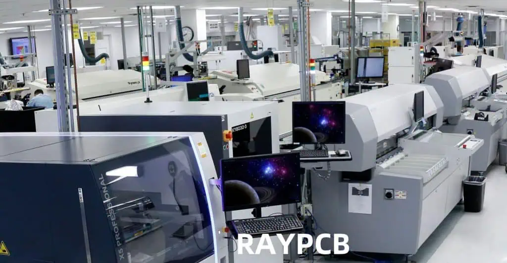
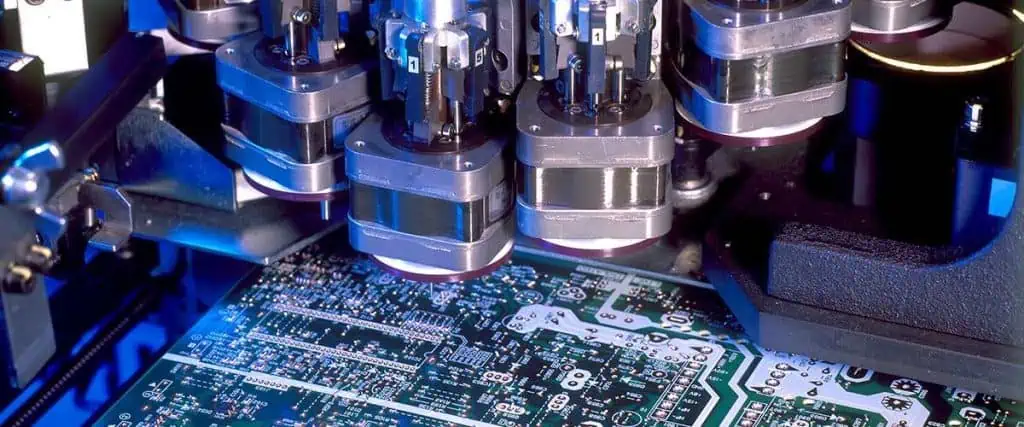
The manufacturing industry focuses on the outcome of the process to earn more profit in lesser time. Hence in the electronics manufacturing industry, where PCBs play a vital role in the development of advance electronic products, PCBs are being manufactured at very high rapid pace. The majority of PCBs we see nowadays are multilayer.
The multilayer PCB mainly composed of SMT components being assembled upon the board by automated setup of robotic arms which use the Pick and place files being generated by PCB layout designer. This pick and place file gives coordinates of each and every electronic component on the PCB and a robot will accurately pick component from reel and place the component on desired location.
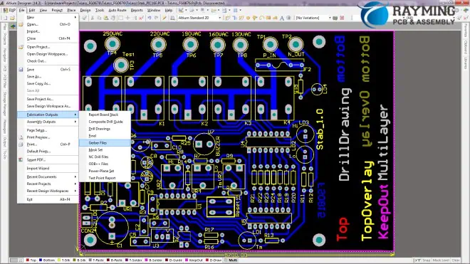
Similarly, the PCB layout design has a specific layer of PCB called “solder paste layer” or “cream” layer. There are top and bottom solder paste layers. Many PCB layout CAD software like Altium and EAGLE have this solder paste layer. This solder paste layer in the PCB layout gives information about the placement of solder paste on the PCB pads.
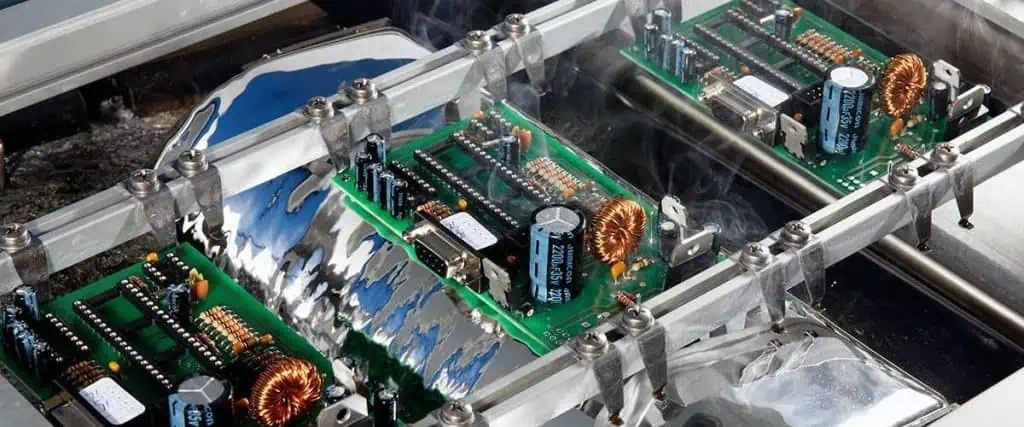
As we know that the SMT components do not have legs so these components needs solder paste to be applied on solder pads before the “reflow soldering” happens. The reflow soldering is the method of baking the PCB after application of solder paste and placement of components on PCB by securing them with glue or flux. The reflow oven will give heat treatment in predefined controlled manner called “Temperature Profile”. This controlled temperature will melt the solder paste and make a strong connection between component lead and solder pad.
In this article we will know about the method of applying this solder paste and tools used in the process. The main tool used is called “Solder Paste Stencil”.
The solder paste stencil is the sheet of metal like stainless steel or nickel that has via holes cut very accurately according to the solder paste layer of PCB layout design. This cutting is done by highly precise “laser cutting machine”. This method of laser cutting is costly and requires extra care to properly fix the stencil on the PCB and avoid any movement while applying solder paste. The stainless steel stencil is suitable for large production run where large number of PCBs are needed to be solder pasted. A single PCB stencil of stainless steel can cover up-to thousand PCBs. However this stencil is costly for only few prototype PCB fabrication.
For few pieces of prototype PCB to be fabricated and solder paste screen printed it is recommended to use polyimide stencil which is lot cheaper than stainless steel and is easier to make these polyimide stencils.
You just need to print and cut the solder paste layer on this polyimide sheet using laser.
The stainless steel stencils are however gives high quality results, have trapezoidal opening, but manufacturing speed of stainless steel stencil is slow. The holes made by laser on the sheet of metal is kept a little smaller than the pad size on PCB so that it will not overspread and will not come out of PCB pad boundary.
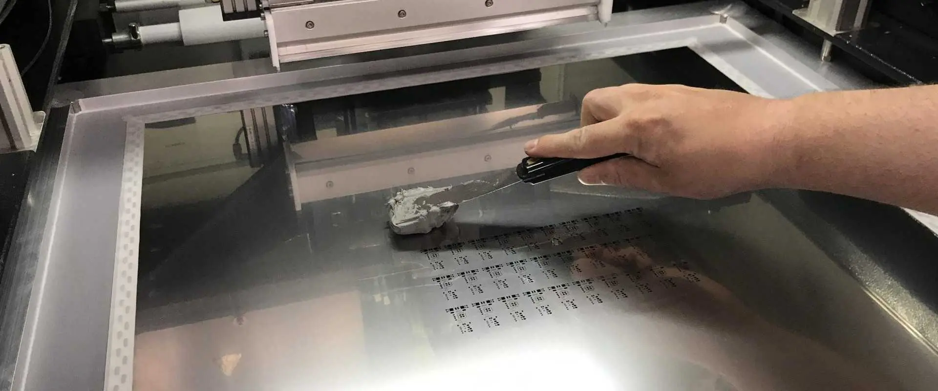
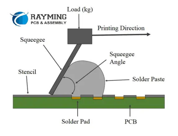
The solder paste is SN63/Pb37 alloy very frequently used as solder for screen printing on PCB pads. This solder paste requires force being applied by the “applicator” or “squeegee” to evenly spread the solder paste on the pads through the aperture walls of stencil.
The amount of solder paste being applied on the pads is proportional to the viscosity of solder paste, aspect and area ratios of stencil.
The Squeegee:
The squeegee is the hard blade of metal use to uniformly spread the solder paste on the stencil to screen print the solder paste on PCB pads. The angle of squeegee against the surface of stencil, pressure or force applied on squeegee and direction of movement of squeegee against the stencil surface will determine how properly the solder paste is applied. The squeegee speed should be 25mm/sec and squeegee force should be 500gm/25mm of squeegee blade length and angle of squeegee should be 60O. The separation speed of stencil after solder paste is applied should be up-to 3mm/sec.
The Stencil Area and Aspect Ratios Formulae:
Types of Solder Paste Stencils:
The stencil can be made of paper, Mylar, polyimide and stainless steel. The thickness and size of aperture opening will determine the amount and volume of solder paste applied. The components like 0603capacitor and resistor and 0.02” pitch SOICs will require thinner stencils while components 1206 and 0.05” capacitor and resistor and ICs package will require thicker stencils. Typically the stencil thickness is 0.005” to 0.007”. The stainless steel stencils are robust and recommended for production run. The aperture opening is recommended to keep less in size than pad size. The aperture opening is about 10% less than the size of the pad. This is done while designing the PCB and the solder paste top and bottom layers in Gerber files are used to print the stencil image on stencil sheet of Mylar or stainless steel or polyimide.
The stencil that comes already fitted inside the fix frame. The frame is a solid or hollow aluminum frame to hold the stencil. These stencils are used for high volume screen printing and is relatively costly. They are recommended for production run. The commonly available size of framed stencil is 20” x 20”.
Frameless Stencil:
These are also called universal stencil and they allow changes to be made to the stencil because stencil is not fixed in any frame. You do not have to completely replace the stencil unlike the framed stencil. Usually the frameless stencil is used for prototype purpose and not for production runs. The users order the frameless stencils usually already have frames that they will attach the stencil manually. They are less expensive than their framed stencil counterparts and requires less storage space.
KiCad is a popular open-source printed circuit board (PCB) design tool used by engineers and hobbyists. After completing a board layout in KiCad, manufacturing output files called Gerber files need to be generated to hand off for PCB fabrication. This article provides a step-by-step guide on properly exporting Gerber files from a KiCad PCB design including setup, configuration, layer mapping, and validation checks.
Overview of Gerber Files
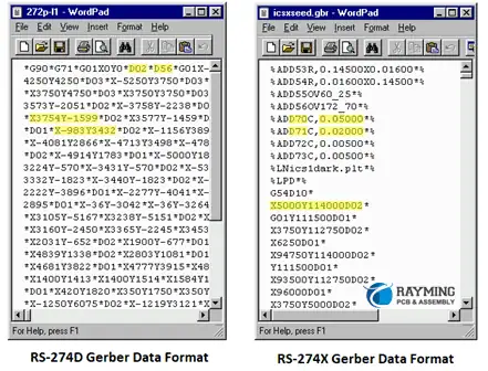
Gerber files are the standard image format used by PCB manufacturers to represent copper layers and other fabrication data for photolithographic reproduction. Key facts about Gerber files:
Subtract mask from silk – Remove soldermask below silkscreen text
Drill Units – Inch or mm Excellon format
Mirror axes – Flip plot to traditional Gerber orientation
Ensure options match requirements of the target PCB fabrication shop.
KiCad Gerber Generation – FAQs
Here are some frequently asked questions about generating Gerber files from KiCad:
What is the standard Gerber mapping convention?
KiCad follows the Protel filename convention like .GTL for Top Layer where the first letter indicates layer and second letter indicates function.
How can Gerber files be validated?
Use a free Gerber viewer like the one built into FlatCAM to visually inspect each file layer, check polarity, confirm board outline, etc.
Do Gerbers require a specific coordinate origin?
The origin set under File → Page Settings when creating the KiCad project will establish the coordinate system zero reference for output files.
What if KiCad is missing needed layers?
Not all fabrication layer types like non-plated holes or finishing notes have default mappings. Custom Gerber jobs can add mappings for any additional files.
How are internal cutouts and holes represented?
KiCad outputs cutouts, slots, and holes as clear polygons or regions in each respective layer file. No additional drill or aperture info is needed.
Conclusion
Exporting properly mapped and validated Gerber files from KiCad provides PCB fabricators the manufacturing information they need to accurately produce a board design. Configuring the layer-to-file mapping table along with output settings generates the correct fabrication files expected from CAD tools. Visually inspecting layers and running design rule checks verifies completeness before release. Taking care to meet Gerber format requirements avoids delays, added costs, or impediments during PCB production. Manufacturing can proceed smoothly with clean verified Gerber output from KiCad designs.
Altium Designer is a popular printed circuit board design tool used by electronics engineers. Two crucial outputs needed from the PCB design process are the bill of materials (BOM) and centroid data file. The BOM lists all components required to build the board while the centroid file provides pick and place machine information on component locations. This article covers how to properly generate and export the BOM and centroid file from an Altium PCB design.
Bill of Materials (BOM)
The bill of materials is one of the most important documents needed to manufacture a PCB assembly. The BOM lists all components required for production along with key details like:
Component designators – Unique IDs like R1, C5, U3 etc.
Description – Component name/value like “10uF capacitor” or “1N4148 diode”
Reference prefix – Code indicating component family like R for resistor
Supplier/Manufacturer – Vendor names for sourcing parts
Packaging info – Reel, cut tape, tray styles for assembly planning
The BOM provides procurement and the assembler every component required in the right quantities to build the board along with vital attributes to ensure the correct parts are sourced.
The centroid file provides exact X-Y location coordinates for every component to facilitate automated pick and place assembly. Key centroid data includes:
Designator – Identifying part code like C7 or U12
Center location – X and Y position relative to assembly origin
Rotation – Angle of rotated parts
Description – Component name and value
This coordinate information allows SMT assembly machines to precisely place components onto PCBs.
Exporting BOM and Centroids from Altium
Altium provides dedicated tools to generate manufacturing BOM and centroid files:
Bill of Materials
Open the compiled PCB document in Altium.
Go to Reports -> Bill of Materials to open the BOM dialog.
Select the needed BOM template like Manufacturing or Procurement.
Choose output format like CSV, Excel, etc.
Set output file save location from dialog or project folder.
Click OK to run generate BOM report.
The BOM can be further processed in spreadsheets if needed for supply chain integration. Detailed fields and custom company templates simplify BOM generation.
Centroid File
With PCB open in Altium, go to File -> Fabrication Outputs -> Centroid File.
Choose file type like CSV or Excel.
Set options like units, precision and rotation format.
Specify filename and location to save centroid data.
Click OK to generate centroid file.
The flexible process supports both through-hole and SMD components. Advanced selections like grouping parts into batches for panelized assemblies is also possible.
BOM Settings and Configuration
BOM of PCB Assembly
Several options exist to tune the exported BOM:
BOM Templates
Use dedicated procurement and assembly templates to include required data
Leverage custom company templates aligned to ERP needs
Specify all component parameters needed by assembly vendor
Parameter Filters
Control which design data parameters show up for each component
For example, include packaging for procurement but not electrical specs
Designator Sorting
Set ordering like reference prefix or component type grouping
Optimized sequence reduces placement changeover during assembly
Board Variants
Generate separate BOM for each assembly variant if using design reuse
Ensure only components on a specific variant are included
Proper BOM configuration reduces errors and manual efforts needed for manufacturing handoff.
Centroid Settings
Key options when generating centroid data:
Units
Specify millimeters (mm) or inches (mil) for coordinate values
Rotation
Degrees or radians options for rotated part angles
Fields
Customize centroid file headers like including package size info
Precision
Set number of decimal places for coordinate values
Layer Types
Include centroids for: top, bottom, both layer parts
Verifying the outputs matches expectations avoids incorrect or incomplete information being sent to procurement and assembly.
BOM/Centroid Generation Automation
Manual BOM and centroid file generation can be automated and streamlined in Altium using:
PCB Panels – Output all boards in a panel array in one action
Design Rule Checks – Execute BOM and centroid run as part of manufacturing DRC validation
Scripts – Write scripts to automate BOM and centroid file output
Version Control – Integrate into ECO release processes and versioned outputs
Output Job Files – Configure presets for one click BOM and centroid file output
This reduces repetitive manual actions for a robust manufacturing handoff process.
Source Control and Versioning
Maintaining properly versioned BOM and centroid data is crucial for quality:
Store files in source control like Git along with project
Include version number in BOM file names like ACME_Widget_A1.2_BOM.csv
Track changes to BOM and centroid files in version history
Associate file revisions with ECO release processes
This linkage provides full manufacturing component and assembly data traceability.
BOM/Centroid Generation – FAQs
Here are some frequently asked questions around generating BOM and centroid files:
How often are BOM/centroid files updated?
BOM and centroid files should be re-generated anytime the schematic or PCB layout changes. This ensures procurement and assembly always have the latest component information.
What if assembly is outsourced?
The designer still provides the BOM and centroids reflecting the designed board to the contract assembler per their requirements. All supporting data helps avoid errors.
Can BOM reference distributor part numbers?
The BOM links to internal company part numbers. Distributor cross-reference info can be optionally included to aid procurement.
What if the PCB panelizes boards?
Panelized arrays output a single centroid file containing all boards. Software maps components to their locations in the panel for assembly.
How are BOM differences resolved?
The PCB BOM authority over schematic BOM. Any discrepancies are flagged for engineers to resolve component mismatches between tools.
Conclusion
The bill of materials and centroid location data are mission critical manufacturing deliverables from the PCB design process. Altium provides dedicated tools to properly generate and export these files by selecting appropriate templates, configuring settings, and customizing output parameters. Cross-validating the BOM and centroids against source data prevents incorrect manufacturing information that can lead to errors during procurement and assembly. Automating and integrating BOM/centroid file output into release processes and version control further enhances traceability and quality. With clean properly configured datahandoffs, manufacturers are set up for first-time-right production of complex electronics.
BOM/Centroid Generation FAQs
What is the difference between a BOM and a Pick and Place file?
The BOM provides the list of components and quantities needed. The Pick and Place file supplies precise X/Y coordinate locations for automated assembly. Both are required from PCB design tools.
What is the typical process for generating BOMs?
BOMs are initially created by the PCB designer then often passed to manufacturing engineers to review and add any missing fabrication and assembly information before release.
How can part reference designators be kept aligned between CAD tools?
Unique component IDs like R27 or C122 should be assigned in the schematic CAD then imported to the PCB layout tool rather than renumbered.
Is supply chain integration used for BOM generation?
BOMs can link to part catalogs, company databases, and ERP systems to automatically pull manufacturer part numbers, datasheets, pricing etc.
How are BOM revision levels maintained?
PCB design tools integrate with version control systems like Git to save BOM file revisions synchronized with project commits providing full version traceability.
Generating Step by Step
Method for Generation of Centroid File and Bill of Material from Altium
Altium tool is very handy in the generation of Bill of Material (BOM) and Electronic Component Placement List (CPL) which is also referred as Centroid file. The following is the way to go.
All you need to know about Bill of Material
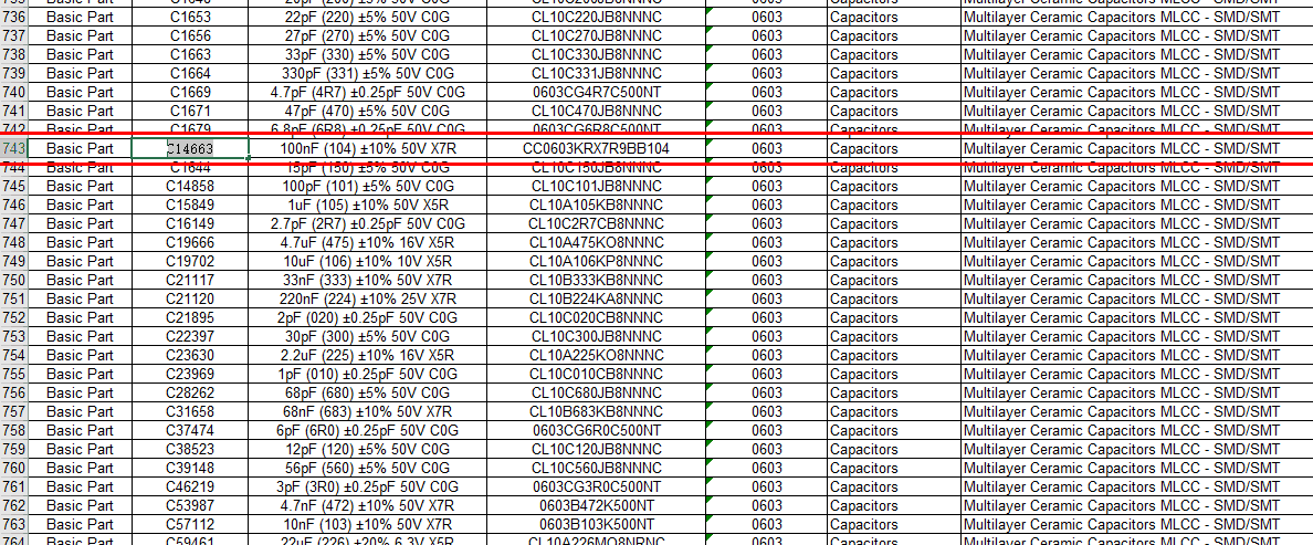
The BOM file is telling the manufacturer about the components which must be installed on the PCB. The BOM is also having information of the exact locations of the components. For instance, there are different points on PCB such as T1, R1, and C1 etc. which depicts the location of components such as resistor, capacitor, inductor, and transistor etc. The information is present in the Bill of Material file and is very important for the assembly process. BOM is generally a simple text format file to be opened in excel having comma separated (CSV) form. This file can also be opened in any other software tool supporting spreadsheets. The following figure is an example of BOM file.
From the figure above, it can be seen that the first column is having information of the values of capacitors and the column is named as “comment”. The comment section should have as much details as possible such as tolerance and maximum allowable voltage information etc. This is for allowing the manufacturing staff to have information of the perfect component to be used for the project. The next column name is “designator” which has information of the position of the component on PCB so that component is soldered at accurate place. Third column is “footprint” and it is also referred as “package” having information of the SMD components having different sizes. Therefore, manufacturing staff is able to know about the size of component to be best fit for PCB. There are different sizes of the SMT components such as 0603, 1206, and 0805 etc. The last column is named as “LCSC part number” which carries information for speeding up the process to get accurate results. RayPCB is having a very large library of components having a unique number. These unique part numbers can be utilized for the identification of accurate part needed.
For saving time in forthcoming projects, the “LCSC part number” can also be added in to the CAD software. In this way when the BOM list is generated next time, the components will be assigned with their unique numbers and it will save time in future.
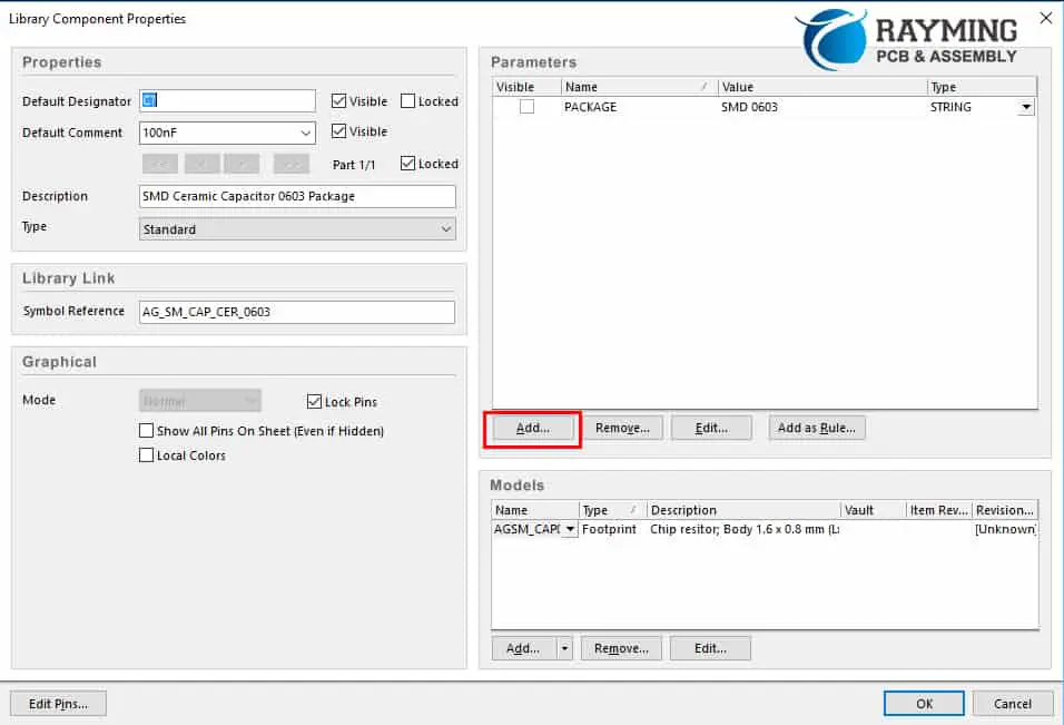
This article is having detailed information of adding the LCSC part number in Altium tool, however same can also be done in other EDA tools as well. First step is opening of the integrated library project which has the required parts such as capacitors, resistors, and inductors etc. The file is named with any unique name such as XBASIC. However, this project is containing two major parts i.e. the schematics symbol and the other is PCB footprints. The file with the symbols of schematics should be opened having an extension (.SchLib). Next step is going to the tab of schematics library.
The tab is having information of all required parts in the library, for instance by selecting the SMD Ceramic Capacitor having 0603 size, double clicking it will open up its entire properties.
Now, in the area of parameters, you have to click on the “add” option for adding the new parameter for the part. This can be illustrated in image below.
After this adding the new parameter is done. Now name it as “LCSC Par # XX” and then put the designated value for the part such as “C0000”.
The value of the LCSC part number form can be acquired from the website of RayPCB as there is a list of about 35,000 different components.
Similarly, the LCSC part number can be added in to all of the parts of the project easily to make the assembly process of future projects smooth.
Generation of Bill of Material File
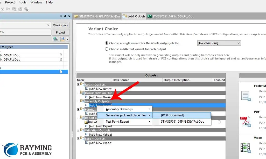
The Bill of Material can also be generated like all other files such as drill and gerber files. The BOM file is generated with the help of “output job file” when Altium tool is considered. Therefore, the use of output job file must be incorporated.
Click on the projects, go to “add new to project” and then select the option of “output job file” as illustrated in figure below.
By choosing options above, job file will be added to the project underway and while using it you are able to generate numerous output files. Here, special focus is made on the generation of BOM file, therefore it will be discussed.
Therefore, by clicking on “add new report”, selecting “bill of materials” and then choose “project”. This process is shown in figure below.
In the generation of BOM, there is an option for adding the column with parameters, as shown below.
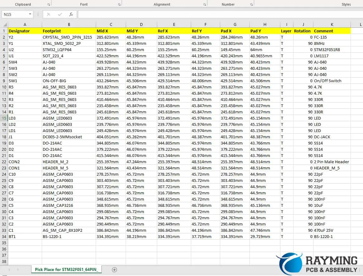
By the use of same output job file, centroid file can also be generated. As discussed already, centroid file is also known as Pick and Place or Placement of Component file. The image below is showing the method.
Figure below is showing setup for making centroid file.
After clicking on the generate content, you have to go to the folder where all files of the project are saved and pick the file named pick place with .csv format.
In the ever-evolving landscape of electronics manufacturing, Printed Circuit Board (PCB) inspection stands as a cornerstone of quality assurance. As we approach 2025, the importance of robust PCB inspection processes has never been more critical. But what exactly is PCB inspection, and why does it matter so much in modern electronics production?
PCB inspection is the systematic examination of printed circuit boards to ensure they meet design specifications, quality standards, and functional requirements. This process is vital in identifying defects, inconsistencies, and potential failure points before a PCB is integrated into a final product. With the increasing complexity of electronic devices and the demand for higher reliability across industries, PCB inspection has become an indispensable step in the manufacturing process.
This comprehensive guide will delve into the methods, techniques, and best practices of PCB inspection as we look ahead to 2025. We’ll explore the various inspection technologies available, from traditional visual inspections to cutting-edge automated systems. Moreover, we’ll discuss why PCB inspection is more crucial than ever, given the trends towards miniaturization and the stringent quality requirements in sectors like automotive, aerospace, and medical devices.
As PCBs continue to grow in complexity, with denser component placement and finer traces, the need for advanced inspection techniques has risen correspondingly. This guide aims to equip manufacturers, engineers, and quality control professionals with the knowledge to navigate the challenges and opportunities in PCB inspection, ensuring the production of high-quality, reliable electronic products in the years to come.
PCB inspection is a critical quality control process in electronics manufacturing that involves examining printed circuit boards for defects, errors, and compliance with design specifications. The primary purpose of PCB inspection is to ensure that each board meets the required standards of quality and functionality before it moves on to the next stage of production or is integrated into a final product.
Importance in Quality Control and Product Reliability
The significance of PCB inspection in maintaining quality control and enhancing product reliability cannot be overstated. Here’s why it’s so crucial:
Defect Detection: Early identification of issues allows for timely corrections, reducing the risk of product failure in the field.
Cost Reduction: Catching problems early in the production process is far less expensive than dealing with failures in assembled products or returns from customers.
Yield Improvement: Regular inspection helps identify recurring issues, allowing for process improvements that increase overall production yield.
Compliance Assurance: Inspection ensures that PCBs meet industry standards and regulatory requirements, which is crucial for sectors like medical devices and aerospace.
Customer Satisfaction: Reliable products lead to satisfied customers and a stronger brand reputation.
Common Defects Detected Through PCB Inspection
PCB inspection processes are designed to catch a wide range of potential defects. Some of the most common issues include:
Soldering Problems:
Solder bridges (unwanted connections between solder points)
Insufficient solder
Cold solder joints
Solder voids
Component Issues:
Misaligned or missing components
Incorrect component placement
Wrong polarity
Damaged components
PCB Substrate Defects:
Cracks or breaks in the board
Delamination
Warpage
Trace and Pad Defects:
Open circuits
Short circuits
Lifted pads
Broken traces
Manufacturing Residues:
Flux residue
Foreign material contamination
Dimensional Issues:
Incorrect board thickness
Misaligned drill holes
By effectively identifying these and other defects, PCB inspection plays a pivotal role in ensuring the quality and reliability of electronic products.
2. Why PCB Inspection Matters More Than Ever in 2025
As we approach 2025, several factors are converging to make PCB inspection more critical than ever before. Let’s explore the key reasons why this process has become increasingly important in the electronics manufacturing landscape.
Increasing Miniaturization of Electronics
The trend towards smaller, more compact electronic devices continues unabated. This miniaturization presents several challenges for PCB manufacturing and inspection:
Denser Component Placement: With more components packed into smaller spaces, the risk of defects like solder bridges or misalignments increases.
Finer Traces and Smaller Vias: As PCB features become smaller, they become more difficult to inspect visually, requiring more advanced inspection techniques.
Increased Complexity: Multi-layer boards with intricate designs are becoming more common, necessitating more thorough inspection processes.
Demand for Higher Reliability
Certain industries have always demanded high reliability from their electronic components. However, this requirement is now spreading to a broader range of sectors:
Automotive Industry: With the rise of electric and autonomous vehicles, the number of PCBs per vehicle is increasing, and each must meet stringent reliability standards.
Aerospace: PCBs used in aircraft and spacecraft must withstand extreme conditions and have near-zero failure rates.
Medical Devices: From implantable devices to diagnostic equipment, medical PCBs require exceptional reliability to ensure patient safety.
Consumer Electronics: As devices become more integral to daily life, consumers expect longer-lasting, more reliable products.
Compliance with International Standards
The regulatory landscape for electronics manufacturing is becoming increasingly complex. Rigorous PCB inspection is essential for compliance with various standards:
IPC-A-610: This standard for PCB assembly has become more stringent in its latest revisions.
ISO 9001: Quality management systems require thorough inspection processes.
Industry-Specific Standards: Different sectors (e.g., medical, automotive) have their own stringent requirements.
Proper inspection ensures that PCBs meet these standards, avoiding costly non-compliance issues.
Cost Savings: Early Detection Reduces Rework and Scrap Rates
In 2025, with increasing pressure on profit margins, the financial benefits of thorough PCB inspection are more apparent than ever:
Reduced Rework: Catching defects early in the production process is far less expensive than reworking assembled products.
Lower Scrap Rates: Effective inspection minimizes the number of PCBs that must be discarded due to undetected defects.
Warranty Cost Reduction: Fewer field failures mean lower warranty claim costs and better customer satisfaction.
Process Improvement: Data from inspections can be used to refine manufacturing processes, leading to long-term cost savings.
Adaptation to New Materials and Technologies
As new PCB materials and manufacturing technologies emerge, inspection processes must evolve to address unique challenges:
Flexible and Rigid-Flex PCBs: These require specialized inspection techniques to ensure quality across different materials and bending points.
High-Frequency PCBs: Used in 5G and other advanced applications, these boards require precise impedance control and tight tolerances, necessitating advanced inspection methods.
Embedded Components: As more PCBs incorporate embedded passive and active components, inspection must adapt to verify these hidden elements.
Environmental Considerations
With growing emphasis on sustainability, PCB inspection plays a role in environmental responsibility:
Energy Efficiency: Ensuring PCBs are correctly manufactured contributes to the energy efficiency of the final products.
Compliance with Environmental Regulations: Proper inspection helps ensure adherence to regulations like RoHS and REACH.
In conclusion, as we look towards 2025, PCB inspection is not just a quality control measure but a critical process that impacts product reliability, regulatory compliance, financial performance, and environmental responsibility. The increasing complexity of electronic devices, coupled with higher expectations for performance and longevity, makes robust PCB inspection more important than ever in ensuring the success of electronics manufacturing ventures.
As PCB technology advances, so do the methods used to inspect them. In 2025, manufacturers have a range of inspection techniques at their disposal, each with its own strengths and ideal applications. Let’s explore the primary types of PCB inspection methods.
3.1 Manual Visual Inspection (MVI)
How it Works
Manual Visual Inspection (MVI) is the most traditional form of PCB inspection. It involves trained inspectors visually examining PCBs for defects, often with the aid of magnification tools.
Tools Used:
Magnifying glasses
Stereo microscopes
Illuminated magnifiers
High-resolution cameras with display screens
Pros and Cons
Pros:
Low initial investment
Effective for detecting visible surface defects
Flexible and adaptable to different PCB types
Can catch unexpected or unusual defects that automated systems might miss
Cons:
Time-consuming, especially for complex boards
Subject to human error and fatigue
Inconsistent results between different inspectors
Limited effectiveness for small components or hidden defects
Best Practices to Improve Accuracy
Proper Lighting: Use adjustable, high-quality lighting to enhance visibility of defects.
Regular Breaks: Implement scheduled breaks to combat eye strain and fatigue.
Standardized Procedures: Develop and follow consistent inspection checklists and procedures.
Ongoing Training: Regularly train inspectors on new components and potential defects.
Ergonomic Workstations: Design inspection areas to minimize physical strain on inspectors.
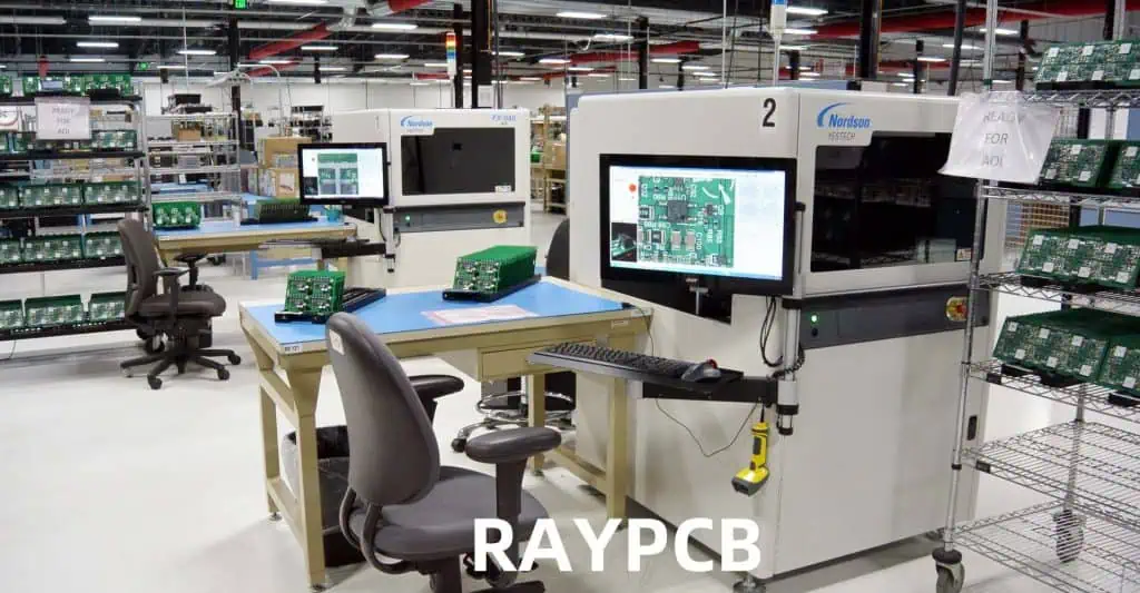
3.2 Automated Optical Inspection (AOI)
Principles of AOI Technology
Automated Optical Inspection uses cameras and image processing software to automatically detect defects on PCBs. It compares captured images of the PCB against a known good board or CAD data to identify anomalies.
Inline vs Offline AOI
Inline AOI: Integrated directly into the production line, inspecting boards as they move through the manufacturing process.
Offline AOI: Separate from the production line, used for more detailed inspection or for smaller production runs.
2D vs 3D AOI in 2025: Latest Advances
2D AOI: Traditional method, effective for detecting surface-level defects.
3D AOI: Uses multiple cameras or laser technology to create a three-dimensional image of the PCB, allowing for more accurate inspection of component height, coplanarity, and solder joint quality.
Latest Advances:
Higher resolution cameras for detecting smaller defects
Improved AI algorithms for defect classification
Integration with factory automation systems for real-time process control
Speed: Can inspect hundreds of points per second, much faster than manual inspection.
Repeatability: Consistent results across multiple inspections and different boards.
High Defect Detection Rates: Can detect a wide range of defects with high accuracy.
Data Collection: Provides valuable data for process improvement and traceability.
3.3 X-ray Inspection (AXI)
When and Why to Use X-ray Inspection
X-ray inspection is crucial for examining internal structures of PCBs and components that are not visible to optical inspection methods. It’s particularly useful for:
Inspecting BGAs (Ball Grid Arrays) and other hidden solder joints
Checking for voids in solder connections
Examining multi-layer boards for internal defects
Detecting Hidden Defects
AXI can detect a variety of hidden defects, including:
Solder bridges under BGA components
Voids in solder joints
Misalignment of internal layers in multi-layer PCBs
Broken internal connections or vias
Differences Between 2D, 2.5D, and 3D X-ray Inspections
2D X-ray:
Provides a top-down view of the PCB
Useful for basic solder joint inspection
Limited in detecting issues in overlapping components
2.5D X-ray:
Combines multiple 2D images taken at different angles
Offers better visibility of solder joints under components
Improves detection of solder voids and bridges
3D X-ray (Computed Tomography):
Creates a full three-dimensional model of the PCB
Allows for “slicing” through the board to examine specific layers
Highest level of defect detection, especially for complex, multi-layer boards
3.4 Flying Probe Testing (FPT)
How Flying Probe Systems Work
Flying Probe Testing uses mobile test probes to make contact with specific points on the PCB, checking for electrical continuity and component values. The probes “fly” from point to point based on the PCB design data.
Ideal Applications: Prototypes, Low-Volume Production
FPT is particularly well-suited for:
Prototype PCBs where creating a dedicated test fixture isn’t cost-effective
Low-volume production runs
Complex boards with dense component placement
Boards that undergo frequent design changes
Key Advantages:
No need for expensive, custom test fixtures
Highly flexible, easily adaptable to different PCB designs
Can test hard-to-reach points on densely populated boards
3.5 In-Circuit Testing (ICT)
How ICT Differs from Flying Probe Testing
In-Circuit Testing uses a bed-of-nails fixture, a custom-made array of pins that makes contact with specific points on the PCB simultaneously. This allows for faster testing compared to Flying Probe methods.
Rapid test execution, often just a few seconds per board
Comprehensive testing of both passive and active components
Ability to detect both manufacturing defects and component failures
High repeatability and consistency in test results
Considerations:
Requires a custom fixture for each PCB design, which can be costly
Less flexible than FPT for design changes
May have limitations for very densely packed boards
3.6 Functional Testing (FCT)
End-Product Functionality Validation
Functional Testing goes beyond checking individual components or connections. It validates that the PCB performs its intended functions as part of the final product.
Where Functional Testing Fits in the Inspection Process
FCT typically occurs after other inspection methods, often as one of the final steps before the PCB is integrated into the end product. It can include:
Powering up the board and checking for correct voltage levels
Testing communication interfaces (e.g., USB, Ethernet)
Verifying sensor inputs and actuator outputs
Running software-based tests to check overall functionality
Importance:
Catches issues that might be missed by other inspection methods
Ensures the PCB will work correctly in its intended application
Can simulate real-world conditions to test durability and performance
In 2025, a comprehensive PCB inspection strategy often involves a combination of these methods, tailored to the specific requirements of the product, production volume, and quality standards. By leveraging the strengths of each inspection technique, manufacturers can ensure the highest level of quality and reliability in their PCB production.
4. Techniques and Tools for Effective PCB Inspection
As we delve deeper into the world of PCB inspection, it’s crucial to understand the specific techniques and tools used to ensure the quality and reliability of printed circuit boards. In 2025, these methods have become more sophisticated, leveraging advanced technologies to detect even the most minute defects. Let’s explore some of the key techniques and tools used in effective PCB inspection.
4.1 Solder Joint Inspection
Solder joint quality is paramount in PCB manufacturing, as poor solder joints are a common cause of PCB failure. Here are some techniques for identifying various solder joint issues:
Techniques for Identifying Solder Bridges, Voids, and Cold Joints
Visual Inspection for Solder Bridges:
Use high-magnification cameras or microscopes to detect unwanted connections between solder points.
Look for excess solder forming a bridge between adjacent pads or leads.
X-ray Inspection for Voids:
Employ X-ray systems to detect voids within solder joints, especially for hidden joints like those in BGAs.
Analyze X-ray images for dark spots within the solder, indicating air pockets or voids.
Thermal Imaging for Cold Joints:
Use infrared cameras to detect temperature differences that may indicate cold solder joints.
Look for joints that heat up more slowly or to a lower temperature than surrounding joints.
3D AOI for Solder Joint Profile:
Utilize 3D AOI systems to create a three-dimensional model of solder joints.
Analyze the shape and volume of solder to ensure proper formation an
Cross-Sectioning for In-Depth Analysis:
For critical applications or troubleshooting, use physical cross-sectioning of solder joints.
Examine the internal structure of joints to assess intermetallic compound formation and void distribution.
4.2 Trace and Pad Inspection
Ensuring the integrity of PCB traces and pads is crucial for the overall functionality and reliability of the board. Here are key techniques for this aspect of inspection:
Importance of Checking PCB Traces, Vias, and Pads for Continuity and Quality
Automated Optical Inspection (AOI) for Surface Traces:
Use high-resolution cameras to detect breaks, narrowing, or other defects in surface traces.
Compare against CAD data to ensure trace width and spacing meet design specifications.
X-ray Inspection for Internal Layers:
Employ X-ray systems to examine traces and vias in internal layers of multi-layer PCBs.
Look for disconnections, misalignments, or other defects not visible from the surface.
Electrical Testing for Continuity:
Use flying probe or in-circuit testers to verify electrical continuity of traces and vias.
Check for opens, shorts, and resistance values that fall outside acceptable ranges.
3D Profilometry for Pad Height and Coplanarity:
Utilize laser or structured light 3D scanning to measure pad height and ensure coplanarity.
Verify that pads meet specifications for subsequent assembly processes like component placement.
Microsectioning for Via Quality:
For critical applications, perform microsectioning to examine the internal structure of vias.
Assess plating thickness, void presence, and overall via formation quality.
4.3 Component Placement and Polarity Verification
Ensuring correct component placement and polarity is essential for PCB functionality. Here are techniques to detect misplaced or rotated components:
How to Detect Misplaced or Rotated Components
2D AOI for Component Presence and Position:
Use pattern matching algorithms to verify component presence and correct positioning.
Compare component outlines and markings against reference images.
3D AOI for Component Height and Coplanarity:
Employ 3D scanning to measure component height and ensure proper seating on the board.
Check for tilted or lifted components that may indicate placement issues.
Fiducial Recognition for Alignment Verification:
Utilize fiducial markers on the PCB to verify overall alignment accuracy of component placement.
Ensure components are placed within specified tolerances relative to these reference points.
Polarity Checking with OCR and Pattern Matching:
Use Optical Character Recognition (OCR) to read component markings and verify correct orientation.
Employ pattern matching to check for polarity indicators like diode bands or pin 1 markers.
X-ray Inspection for Hidden Components:
Use X-ray systems to verify correct placement and orientation of BGAs and other hidden components.
Check for proper alignment of internal structures like solder balls or lead frames.
4.4 3D Inspection Technologies
As PCBs become more complex, 3D inspection technologies have become increasingly important. Here’s an overview of the latest advancements:
Use of 3D Profilometry and Laser Measurement in 2025
Structured Light 3D Scanning:
Projects a pattern of light onto the PCB surface and analyzes its deformation to create a 3D model.
Provides high-resolution data on surface topography, component height, and solder joint profiles.
Laser Triangulation:
Uses laser line projection and camera imaging to create precise 3D measurements.
Excellent for measuring component height, coplanarity, and solder paste volume.
Confocal Microscopy:
Employs optical sectioning to create high-resolution 3D images of small features.
Useful for inspecting fine-pitch components and analyzing surface textures.
Multi-Angle and Multi-Spectral Imaging:
Combines images from multiple angles and light spectra to create comprehensive 3D models.
Enhances defect detection capabilities, especially for complex geometries and varied materials.
AI-Enhanced 3D Analysis:
Utilizes machine learning algorithms to interpret 3D scan data and identify defects.
Improves detection accuracy and reduces false positives in 3D inspection processes.
These advanced 3D inspection technologies allow for more precise measurements and better detection of defects related to component placement, solder joint quality, and overall board topology. They are particularly valuable for inspecting complex, densely populated PCBs and for ensuring compliance with increasingly stringent manufacturing standards.
By employing these techniques and tools, PCB manufacturers can significantly enhance their inspection capabilities, ensuring higher quality products and reducing the risk of field failures. As we move further into 2025 and beyond, we can expect these technologies to become even more sophisticated, with increased integration of AI and machine learning to further improve defect detection and process control in PCB manufacturing.
5. Common PCB Defects Found During Inspection
As PCB designs become more complex and manufacturing processes more advanced, the types of defects that can occur during production have also evolved. In 2025, PCB inspection processes are designed to catch a wide array of potential issues. Understanding these common defects is crucial for maintaining high-quality standards in PCB manufacturing. Let’s explore the main categories of defects typically found during PCB inspection:
Description: Unintended connections between circuit points.
Causes: Solder bridges, conductive contamination, or design errors.
Detection: In-circuit testing, flying probe testing, and power-on testing.
Open Circuits:
Description: Breaks in intended electrical pathways.
Causes: Broken traces, lifted pads, or incomplete solder joints.
Detection: Electrical continuity testing, flying probe testing, and functional testing.
High Resistance Connections:
Description: Connections with higher than expected resistance.
Causes: Poor soldering, oxidation, or partial breaks in traces.
Detection: Precision resistance measurement, thermal imaging during power-on.
Leakage Currents:
Description: Unintended current flow between isolated circuit sections.
Causes: Contamination, moisture ingress, or insulation breakdown.
Detection: Insulation resistance testing, specialized leakage current tests.
Additional Common Defects
Solder Paste Issues:
Insufficient or excess solder paste
Smeared or misaligned solder paste deposits
Detection: Solder paste inspection (SPI) systems
Via Defects:
Incomplete plating
Voids in via fill
Detection: X-ray inspection, microsectioning for critical applications
Pad Lift-Off:
Description: Separation of copper pads from the PCB substrate
Causes: Excessive heat during rework, poor adhesion in manufacturing
Detection: Visual inspection, stress testing
Tombstoning:
Description: One end of a component lifts off the pad during soldering
Causes: Uneven heating, pad design issues, or component placement problems
Detection: AOI, visual inspection
Foreign Object Debris (FOD):
Description: Unwanted particles or objects on the PCB
Causes: Contamination during manufacturing or handling
Detection: Visual inspection, AOI
Understanding these common defects is crucial for developing effective inspection strategies and improving overall PCB quality. In 2025, the integration of AI and machine learning into inspection systems is enhancing the ability to detect and classify these defects accurately and efficiently. This not only improves the quality of individual PCBs but also provides valuable data for continuous improvement of the manufacturing process.
6. Best Practices for PCB Inspection in 2025
As we navigate the complexities of PCB manufacturing in 2025, implementing best practices in inspection processes is crucial for ensuring high-quality, reliable products. These practices not only help in detecting defects but also in preventing them and optimizing the overall manufacturing process. Let’s explore the key best practices for PCB inspection:
Design for Inspection (DFI): Designing PCBs with Inspection in Mind
Incorporate Test Points:
Include dedicated test points in PCB designs to facilitate easier electrical testing.
Ensure test points are accessible for both automated and manual inspection methods.
Optimize Component Placement:
Design layouts that allow for clear visual access to components and solder joints.
Avoid placing small components under larger ones where possible.
Use Fiducial Markers:
Include fiducial markers to aid in alignment during automated inspection processes.
Place fiducials strategically for maximum effectiveness in component placement verification.
Consider X-ray Inspection Requirements:
For boards with BGAs or other hidden solder joints, design with X-ray inspection in mind.
Avoid overlapping components that could obscure X-ray views of critical areas.
Standardize Pad Designs:
Use consistent pad designs where possible to simplify automated inspection programming.
Ensure pad sizes and shapes are optimized for both soldering and inspection processes.
Choosing the Right Inspection Method Based on Volume, Complexity, and Cost
Assess Production Volume:
For high-volume production, invest in automated systems like AOI and AXI.
For low-volume or prototype runs, consider more flexible options like flying probe testing.
Evaluate Board Complexity:
For complex, multi-layer boards, incorporate X-ray inspection into the process.
Use 3D AOI for boards with a high mix of component types and sizes.
Consider Cost-Effectiveness:
Balance the cost of inspection equipment against the potential cost of field failures.
Factor in the long-term benefits of data collection and process improvement capabilities.
Adapt to Product Lifecycle:
Implement more rigorous inspection processes during new product introduction phases.
Adjust inspection strategies as products mature and processes stabilize.
Combining Multiple Inspection Methods for Maximum Reliability
Implement a Multi-Stage Inspection Process:
Use SPI (Solder Paste Inspection) before component placement.
Follow with AOI after placement and reflow.
Incorporate AXI for critical or hidden joints.
Finish with ICT or functional testing.
Tailor Inspection Combinations to Product Requirements:
For high-reliability products (e.g., medical, aerospace), use a combination of visual, AOI, AXI, and electrical testing.
For consumer electronics, balance speed and cost with an appropriate mix of automated and sampling-based inspections.
Use Data Integration:
Implement systems that allow data sharing between different inspection stages.
Utilize this integrated data for comprehensive defect analysis and process improvement.
Training and Certification for Inspection Personnel
Develop Comprehensive Training Programs:
Provide in-depth training on PCB technology, common defects, and inspection equipment.
Include hands-on practice with a variety of PCB types and potential defects.
Pursue Industry Certifications:
Encourage staff to obtain relevant certifications (e.g., IPC Certification).
Support ongoing education to keep up with evolving technologies and standards.
Implement Regular Skill Assessments:
Conduct periodic evaluations of inspector performance and knowledge.
Use results to tailor ongoing training and development programs.
Foster a Culture of Continuous Learning:
Encourage knowledge sharing among team members.
Provide opportunities for inspectors to learn about new technologies and industry trends.
Maintaining and Calibrating Inspection Equipment
Establish Regular Calibration Schedules:
Develop and adhere to calibration schedules for all inspection equipment.
Use traceable standards for calibration processes.
Perform Routine Maintenance:
Implement preventive maintenance programs for all inspection systems.
Keep detailed maintenance logs and track equipment performance over time.
Verify Equipment Accuracy:
Regularly use known good boards and known defect boards to verify inspection system performance.
Adjust and fine-tune systems as needed based on these verifications.
Stay Current with Software Updates:
Keep inspection system software up-to-date to benefit from the latest algorithms and features.
Evaluate and implement new software capabilities that can enhance inspection accuracy or efficiency.
Monitor Environmental Conditions:
Ensure inspection areas maintain stable temperature and humidity levels.
Use environmental monitoring systems to track and log conditions that could affect inspection accuracy.
Implementing Continuous Improvement Processes
Analyze Inspection Data:
Regularly review data from all inspection stages to identify trends and recurring issues.
Use statistical process control (SPC) methods to monitor and improve manufacturing processes.
Conduct Root Cause Analysis:
For significant or recurring defects, perform thorough root cause analysis.
Implement corrective actions based on these analyses to prevent future occurrences.
Foster Collaboration Between Departments:
Encourage regular meetings between design, manufacturing, and quality control teams.
Use inspection findings to inform design improvements and manufacturing process adjustments.
Benchmark Against Industry Standards:
Regularly compare your inspection processes and results against industry benchmarks.
Participate in industry forums and associations to stay informed about best practices.
Invest in New Technologies:
Stay informed about advancements in inspection technologies.
Evaluate and implement new technologies that can improve inspection accuracy or efficiency.
7. Trends Shaping the Future of PCB Inspection
As we look towards the future of PCB inspection, several key trends are emerging that promise to revolutionize the field. These advancements are not only improving the accuracy and efficiency of inspection processes but also transforming how manufacturers approach quality control in PCB production. Let’s explore the major trends shaping the future of PCB inspection in 2025 and beyond.
AI and Machine Learning in Automated Inspections
Artificial Intelligence (AI) and Machine Learning (ML) are rapidly becoming integral parts of PCB inspection systems, offering unprecedented levels of accuracy and efficiency.
Advanced Defect Detection:
AI algorithms can identify complex defect patterns that might be missed by traditional rule-based systems.
Machine learning models continually improve their detection capabilities as they process more data.
Adaptive Inspection Parameters:
AI systems can automatically adjust inspection parameters based on board type, component density, and historical data.
This adaptability reduces the need for manual programming and improves inspection accuracy across diverse product lines.
Anomaly Detection:
ML algorithms excel at identifying unusual patterns or defects that don’t fit known categories.
This capability is particularly valuable for detecting new or rare defect types.
Predictive Maintenance:
AI can analyze inspection system performance data to predict maintenance needs, reducing downtime.
This proactive approach ensures consistent inspection quality and extends equipment lifespan.
Real-time Process Optimization:
AI systems can analyze inspection data in real-time to suggest process adjustments, reducing defect rates on the fly.
Integration of PCB Inspection into Smart Manufacturing (Industry 4.0)
The concept of Industry 4.0 is transforming PCB manufacturing, with inspection playing a crucial role in this digital transformation.
Connected Inspection Systems:
Inspection equipment is increasingly integrated with other manufacturing systems, allowing for seamless data exchange.
This connectivity enables real-time monitoring and control of the entire production process.
Digital Twin Technology:
Virtual models (digital twins) of PCBs and manufacturing processes are used to simulate and optimize inspection strategies.
These models can predict potential defects and guide targeted inspection efforts.
Cloud-Based Data Management:
Inspection data is stored and analyzed in cloud platforms, allowing for global access and advanced analytics.
This centralized approach facilitates better collaboration and decision-making across multiple manufacturing sites.
Internet of Things (IoT) sensors monitor environmental conditions that could affect PCB quality or inspection accuracy.
Real-time data from these sensors can trigger automatic adjustments in manufacturing or inspection processes.
Augmented Reality in Manual Inspections:
AR technologies assist human inspectors by overlaying digital information onto physical PCBs.
This can guide inspectors to potential problem areas and provide real-time reference information.
Predictive Analytics to Anticipate Failure Points Before They Occur
Predictive analytics is moving PCB inspection from a reactive to a proactive approach, helping manufacturers identify potential issues before they become actual defects.
Early Warning Systems:
Advanced analytics models analyze historical and real-time data to predict potential defects or process deviations.
These systems can alert operators to take preventive action before quality issues occur.
Lifecycle Prediction:
Predictive models can estimate the expected lifespan and reliability of PCBs based on inspection data and usage patterns.
This information is valuable for both manufacturers and end-users in planning maintenance and replacements.
Supply Chain Integration:
Predictive analytics extend beyond the production floor, integrating data from suppliers to anticipate quality issues related to raw materials or components.
Customer Usage Insights:
Analysis of field data and customer usage patterns can inform inspection criteria, focusing efforts on areas most likely to impact real-world performance.
Continuous Process Improvement:
Predictive models identify subtle trends and correlations in manufacturing data, driving continuous refinement of processes and inspection methods.
Eco-Friendly Inspection Methods and Materials
Environmental considerations are becoming increasingly important in PCB manufacturing and inspection.
Energy-Efficient Inspection Systems:
New inspection technologies are designed with energy efficiency in mind, reducing the carbon footprint of quality control processes.
Reduced Use of Harmful Chemicals:
Inspection methods that reduce or eliminate the need for chemical cleaning or processing are gaining popularity.
Non-Destructive Testing Advancements:
Improvements in non-destructive testing methods reduce waste associated with destructive testing practices.
Recyclable and Biodegradable Materials:
Development of PCB materials that are more easily recyclable or biodegradable, with inspection processes adapted to these new materials.
Water Conservation in Cleaning Processes:
Inspection technologies that reduce the need for water-based cleaning, or that use water more efficiently in necessary cleaning processes.
Miniaturization and Increased Density Challenges
As PCBs continue to shrink while becoming more complex, inspection technologies are evolving to meet these challenges.
High-Resolution Imaging:
Development of ultra-high-resolution cameras and optics to inspect increasingly miniature components and features.
Advanced X-ray Technologies:
Improvements in X-ray resolution and 3D reconstruction capabilities to inspect dense, multi-layer boards.
Nano-scale Inspection Techniques:
Emerging technologies for inspecting nano-scale features and components on advanced PCBs.
Multi-sensor Fusion:
Combining data from multiple sensor types (optical, X-ray, thermal, etc.) to create more comprehensive inspection results.
AI-Enhanced Image Processing:
Using AI to extract meaningful information from complex, high-resolution inspection images of densely packed PCBs.
These trends are not just theoretical concepts but are actively shaping the landscape of PCB inspection in 2025. Manufacturers who embrace these technologies and approaches will be well-positioned to produce higher quality PCBs, reduce defects, and meet the ever-increasing demands of the electronics industry. As these trends continue to evolve, we can expect even more innovative solutions to emerge, further advancing the field of PCB inspection and quality control.
8. How to Choose the Right PCB Inspection Strategy
Selecting the appropriate PCB inspection strategy is crucial for ensuring product quality while maintaining efficiency and cost-effectiveness. In 2025, with a wide array of inspection technologies and methodologies available, making the right choice can be complex. This section will guide you through the key factors to consider and provide a framework for decision-making.
Factors to Consider: Production Volume, Complexity, Budget, Compliance Needs
Production Volume:
High Volume: Favor automated systems like AOI and AXI for speed and consistency.
Low Volume: Consider more flexible options like manual inspection or flying probe testing.
Mixed Production: Look for adaptable systems that can handle varying batch sizes efficiently.
PCB Complexity:
Simple Boards: Basic visual inspection and 2D AOI may be sufficient.
Complex Multi-layer Boards: Incorporate X-ray inspection and 3D AOI.
High-Density Boards: Consider advanced optical and X-ray technologies with high resolution capabilities.
Budget Constraints:
Initial Investment: Balance upfront costs with long-term savings from improved quality and reduced rework.
Operational Costs: Consider ongoing expenses like maintenance, training, and potential upgrades.
Return on Investment: Evaluate how quickly inspection systems will pay for themselves through defect reduction and improved efficiency.
Combination of AOI, AXI, ICT, and Functional Testing
Budget Constraints
Prioritize Critical Areas, Consider Outsourcing
Compliance-Driven
Systems with Strong Data Logging and Traceability
Remember, the ideal inspection strategy often involves a combination of methods, tailored to your specific needs. It’s also important to regularly review and adjust your inspection strategy as technology advances and your production needs evolve.
By carefully considering these factors and using the decision tree and table as guides, you can develop a PCB inspection strategy that balances quality, efficiency, and cost-effectiveness for your specific manufacturing context in 2025 and beyond.
Conclusion
As we’ve explored throughout this comprehensive guide, PCB inspection plays a crucial role in ensuring the quality, reliability, and performance of electronic products in 2025 and beyond. The landscape of PCB manufacturing and inspection continues to evolve rapidly, driven by technological advancements, increasing product complexity, and ever-higher quality standards.
Let’s recap the key points we’ve covered:
The Critical Importance of PCB Inspection: We’ve seen how thorough inspection processes are essential for detecting defects early, reducing costs, and ensuring product reliability across various industries.
Diverse Inspection Methods: From traditional visual inspection to advanced automated systems like AOI, AXI, and 3D scanning technologies, a wide range of tools and techniques are available to address different inspection needs.
Common Defects and Detection Techniques: Understanding the types of defects that can occur in PCBs and the most effective methods for detecting them is crucial for implementing a robust inspection strategy.
Best Practices: We’ve outlined key practices such as designing for inspection, combining multiple inspection methods, and maintaining and calibrating equipment to optimize the inspection process.
Emerging Trends: The integration of AI and machine learning, the move towards smart manufacturing, and the use of predictive analytics are shaping the future of PCB inspection, offering new possibilities for accuracy and efficiency.
Strategic Decision-Making: Choosing the right inspection strategy involves carefully considering factors such as production volume, board complexity, budget constraints, and compliance requirements.
As we look to the future, several key trends will continue to shape PCB inspection:
Increasing Automation and AI Integration: The role of artificial intelligence in defect detection and process optimization will grow, leading to more accurate and efficient inspection processes.
Greater Connectivity and Data Integration: In line with Industry 4.0 principles, PCB inspection will become more integrated with other manufacturing processes, enabling real-time adjustments and improvements.
Advancements in Miniaturization: As PCBs continue to shrink and become more complex, inspection technologies will need to evolve to handle increasingly fine details and dense layouts.
Focus on Sustainability: Eco-friendly inspection methods and materials will gain importance as the industry strives for greater environmental responsibility.
For manufacturers and engineers looking to optimize their inspection processes in 2025 and beyond, here are some final tips:
Stay Informed: Keep abreast of the latest developments in PCB inspection technologies and methodologies. Attend industry conferences, participate in webinars, and engage with technology providers to understand new capabilities.
Invest in Training: Ensure that your team is well-trained not only in operating inspection equipment but also in understanding the principles behind different inspection methods and interpreting results accurately.
Embrace Data-Driven Decision Making: Utilize the wealth of data generated by modern inspection systems to drive continuous improvement in your manufacturing processes.
Be Flexible and Adaptable: As product requirements and technologies change, be prepared to adjust your inspection strategies accordingly. Regular reviews of your inspection processes can help ensure they remain effective and efficient.
Collaborate Across Departments: Foster strong communication between design, manufacturing, and quality control teams. Insights from inspection processes can inform better design practices and manufacturing techniques.
Consider Total Cost of Ownership: When investing in new inspection technologies, look beyond the initial price tag to consider factors like efficiency gains, reduced scrap rates, and improved product quality over time.
Prioritize Traceability: Implement robust systems for tracking and documenting inspection results, which is increasingly important for regulatory compliance and customer satisfaction.
In conclusion, as PCBs continue to play a central role in our increasingly electronic world, the importance of effective inspection cannot be overstated. By leveraging the latest technologies, adhering to best practices, and maintaining a commitment to quality, manufacturers can ensure that their PCBs meet the high standards required in 2025 and beyond. The future of PCB inspection is one of greater precision, efficiency, and integration, promising exciting possibilities for the entire electronics industry.
FAQs
What are the most common PCB inspection methods? The most common PCB inspection methods include Automated Optical Inspection (AOI), X-ray Inspection (AXI), In-Circuit Testing (ICT), Flying Probe Testing, and Manual Visual Inspection. Each method has its strengths and is often used in combination with others for comprehensive quality control.
What is the difference between AOI and AXI inspection? AOI (Automated Optical Inspection) uses cameras and image processing to inspect the surface of PCBs, detecting visible defects like component placement issues or solder problems. AXI (Automated X-ray Inspection) uses X-rays to inspect internal aspects of the PCB, particularly useful for detecting defects in hidden solder joints, like those in BGAs or multi-layer boards.
Can AI improve PCB inspection accuracy? Yes, AI can significantly improve PCB inspection accuracy. Machine learning algorithms can be trained to detect subtle defects that might be missed by traditional inspection methods. AI can also adapt to new defect types, reduce false positives, and improve overall inspection efficiency.
The global electroplating PCB industry’s output value accounts for a rapid increase in the proportion of the total output value of the electronic components industry. It is the industry with the largest proportion of the electronic component segmentation industry, and has a unique position. The annual output value of electroplated PCB is 60 billion US dollars. The volume of electronic products is becoming thinner and lighter, and direct stacking on blind vias is a design method for obtaining high-density interconnects. To make a stack of holes, you should first do a good job at the bottom of the hole. There are several methods for fabricating a typical flat hole surface, and a plating hole filling process is one of them.
https://www.youtube.com/watch?v=c_QpC91z_do
In addition to reducing the need for additional process development, the electroplating and hole-filling process is also compatible with current process equipment, which is beneficial for good reliability.
Electroplating and filling holes have the following advantages:
(1) It is advantageous to design stacked and on-disk holes (Via.on.Pad);
(2) Improve electrical performance and contribute to high frequency design;
(3) Helps to dissipate heat;
(4) The plug hole and the electrical interconnection are completed in one step;
(5) The blind holes are filled with electroplated copper, which has higher reliability and better conductivity than conductive paste.
Physical influence parameter:
The physical parameters that need to be studied are: anode type, anode-anode spacing, current density, agitation, temperature, rectifier, and waveform.
(1)Type of anode. When it comes to anode type, it is nothing more than a soluble anode and an insoluble anode. The soluble anode is usually a phosphorus-containing copper ball, which easily produces anode mud, contaminates the plating solution, and affects the performance of the plating solution. Insoluble anodes, also known as inert anodes, are typically composed of a titanium mesh coated with a mixed oxide of cerium and zirconium. Insoluble anode, good stability, no anode maintenance, no anode mud generation, pulse or DC plating are applicable; however, the additive consumption is large.
(2)The anode-anode spacing. The design of the spacing between the cathode and the anode in the electroplating process is very important, and the design of different types of equipment is not the same. However, it should be pointed out that no matter how the design is, it should not violate the first law of Farah.
(3)Stirring. There are many types of mixing, such as mechanical rocking, electric shock, gas vibration, air agitation, and jet (Eductor).
For electroplating and filling holes, it is generally preferred to increase the jet design in the configuration of conventional copper cylinders. However, whether it is the bottom jet or the side jet, how is the jet pipe and the air agitating pipe arranged in the cylinder; what is the jet flow per hour; how much the jet pipe is spaced from the cathode; if the side jet is used, the jet is at the anode Whether the front or the back; if the bottom jet is used, will it cause uneven mixing, the plating solution is weak and strong; the number, spacing and angle of the jet on the jet tube are factors that must be considered in the design of the copper cylinder, and also A lot of trials are going on.
In addition, the most ideal way is to connect each flow tube to the flowmeter to achieve the purpose of monitoring the flow. Temperature control is also important because the flow rate is large and the solution is prone to heat.
(4)Current density and temperature. Low current density and low temperature can reduce the deposition rate of surface copper while providing sufficient Cu2 and brightener into the pores. Under these conditions, the ability to fill holes is enhanced, but at the same time the plating efficiency is also reduced.
(5) Rectifier. The rectifier is an important part of the electroplating process. At present, the research on electroplating and filling holes is mostly limited to full-plate electroplating. If the pattern plating hole is considered, the cathode area will become small. At this time, high requirements are placed on the output accuracy of the rectifier.
The output accuracy of the rectifier should be chosen according to the line of the product and the size of the via. The finer the lines and the smaller the holes, the higher the accuracy requirements for the rectifier. Generally, a rectifier with an output accuracy of 5% or less should be selected. Exceeding the accuracy of the selected rectifier will increase the investment in the equipment. For the output cable of the rectifier, the rectifier should be placed on the side of the plating tank as much as possible. This can reduce the length of the output cable and reduce the pulse current rise time. The rectifier output cable specification should be chosen to meet the line drop of the output cable within 0.6V at 80% of the maximum output current. The required cable cross-sectional area is usually calculated at a current carrying capacity of 2.5 A/mm:. If the cross-sectional area of the cable is too small or the cable length is too long and the line voltage drop is too large, the current will not reach the current value required for production.
For plating tanks with a groove width greater than 1.6 m, bilateral input should be considered and the length of the bilateral cables should be equal. In this way, it is guaranteed that the bilateral current error is controlled within a certain range. A rectifier should be connected to each side of each fly-bar of the plating tank so that the currents on both sides of the part can be adjusted separately.
(6)At present, from the perspective of waveforms, there are two types of electroplating holes: pulse plating and DC plating. These two methods of electroplating and filling have been studied. The DC electroplating hole is made of a conventional rectifier, which is easy to operate, but if the plate is thick, it is powerless. The pulse plating filling hole adopts the PPR rectifier, and the operation steps are many, but the processing ability for the thicker plate is strong.
Substrate influence
The influence of the substrate on the electroplating and filling holes is also negligible. Generally, there are factors such as dielectric layer material, hole shape, aspect ratio, and chemical copper plating.
(1) Dielectric layer material. The dielectric layer material has an effect on the filling of holes. Non-glass reinforced materials are easier to fill than holes in glass reinforced materials. It is worth noting that the glass fiber protrusions in the holes have an adverse effect on the chemical copper. In this case, the difficulty in electroplating is to increase the adhesion of the electroless plating seed layer, rather than the hole filling process itself.
In fact, electroplating and filling holes on glass fiber reinforced substrates have been used in actual production.
(2)Thickness to diameter ratio. At present, the hole-filling technology for different shapes and different sizes of holes is highly valued by both manufacturers and developers. The hole filling ability is greatly affected by the hole thickness ratio. Relatively speaking, DC systems are more widely used commercially. In production, the size of the hole will be narrower, generally 80pm ~ 120Bm diameter, hole depth 40Bm ~ 8OBm, thickness to diameter ratio does not exceed 1:1.
(3) Electroless copper plating. The thickness and uniformity of the chemical copper plating and the placement time after electroless copper plating all affect the hole filling performance. Chemical copper is too thin or uneven in thickness, and its hole filling effect is poor. Generally, it is recommended to fill holes when the thickness of the chemical copper is >0.3 pm. In addition, the oxidation of chemical copper also has a negative effect on the hole filling effect.
Is Your Current Soldering Process Holding Back Your PCB Designs?
Traditional wave soldering and outdated selective systems often force design compromises – but they don’t have to. Our precision selective soldering solutions deliver:
✔ Pinpoint Accuracy – Target only the required through-hole components while completely avoiding nearby sensitive SMDs ✔ Gentle Processing – Protect delicate packages (QFN, BGAs, connectors) from thermal stress ✔ Engineered Consistency – Automated control of flux deposition, solder volume, and dwell time for perfect joints every time ✔ Reliability Built-In – Proven results for mission-critical applications where joint integrity matters most
Upgrade your assembly capability without redesigning your boards. Let’s discuss how intelligent selective soldering can solve your toughest production challenges.
Defining Selective Soldering
Selective soldering is a specialized method that allows for precise soldering of specific components or areas on a PCB without affecting surrounding parts. This technique is particularly valuable for assembling boards that combine through-hole and surface-mount components.
Key Applications of Selective Soldering
Selective soldering shines in several scenarios:
Mixed-technology PCBs featuring both through-hole and surface-mount devices
Assemblies with temperature-sensitive components that can’t withstand traditional wave soldering
High-density boards where precise solder application is crucial
The Rising Importance of Selective Soldering
Several factors are driving the adoption of selective soldering in the electronics industry:
Miniaturization Trends: As devices shrink, the need for precise, localized soldering increases.
Environmental Regulations: The shift to lead-free solders often requires more controlled soldering processes.
Increasing PCB Complexity: Modern circuits frequently combine various component types, necessitating flexible soldering solutions.
Selective soldering can be performed using various equipment types:
1. Robotic Nozzle Systems
These systems use programmable robots to guide a miniature solder wave nozzle to specific locations on the PCB, offering flexibility for different board layouts.
2. Laser Selective Soldering
Laser systems provide extremely precise heat application, making them ideal for ultra-fine pitch components or areas with tight spacing.
3. Hybrid Selective Soldering Systems
Some machines combine multiple soldering technologies (e.g., mini-wave and laser) to maximize flexibility and handle a wide range of soldering tasks.
Advantages of Selective Soldering
Selective soldering offers numerous benefits over traditional soldering methods:
1. Unmatched Precision
Selective soldering allows for targeted solder application, crucial for:
Avoiding heat-sensitive components
Soldering near delicate parts like connectors or BGAs
2. Exceptional Flexibility
It excels at handling:
Mixed-technology boards
Small to medium production runs
Frequent product changeovers
3. Superior Quality
Compared to wave soldering, selective soldering significantly reduces defects such as:
While selective soldering offers many advantages, it also presents some challenges that need to be addressed:
1. Thermal Management
Challenge: Preventing heat damage to nearby components. Solution: Implement precise control of solder temperature, dwell time, and preheat profiles.
2. Flux Residue Handling
Challenge: Managing flux residues, especially in hard-to-reach areas. Solution: Utilize no-clean fluxes or develop targeted cleaning processes for post-solder cleaning.
3. Shadowing Effects
Challenge: Dealing with obstructed solder joints due to component placement. Solution: Employ angled nozzles or laser soldering techniques for accessing difficult areas.
4. Process Parameter Optimization
Challenge: Fine-tuning parameters for consistent results across different board designs. Solution: Implement closed-loop control systems and regularly validate process parameters through testing.
Best Practices for Effective Selective Soldering
To maximize the benefits of selective soldering, consider these industry-proven best practices:
Design for Manufacturability (DFM)
Optimizing Pad and Via Design
Design pads and vias with adequate spacing for nozzle or laser access.
Implement thermal relief patterns for large pads connected to ground planes to improve heat distribution.
Strategic Component Placement
Ensure sufficient clearance around through-hole components for soldering tool access.
Group similar components to streamline soldering programs and improve efficiency.
Material Selection for Selective Soldering
Choosing Compatible Components
Select components that can withstand the selective soldering thermal profile.
Consider using heat sinks or thermal compounds for sensitive components near solder points.
Selecting Appropriate Fluxes and Alloys
Choose fluxes specifically formulated for selective soldering applications.
Use solder alloys that match your thermal profile and regulatory requirements (e.g., SAC305 for lead-free applications).
Implementing Robust Process Validation
Comprehensive Solder Joint Inspection
Utilize Automated X-ray Inspection (AXI) or Automated Optical Inspection (AOI) for thorough joint quality assessment.
Implement regular visual inspections to catch any anomalies that automated systems might miss.
Periodic Cross-Sectional Analysis
Conduct regular cross-sectional analysis of solder joints to verify internal structure and long-term reliability.
Industry Applications of Selective Soldering
Selective soldering has found applications across various industries:
1. Automotive Electronics
Used in manufacturing complex ECUs (Electronic Control Units) and sensor-rich assemblies where precision and reliability are paramount.
2. Aerospace and Defense
Critical for producing high-reliability assemblies in avionics, satellite systems, and military communications equipment.
3. Medical Devices
Enables the production of miniaturized, high-precision medical devices and implantables that require exceptional reliability.
4. Consumer Electronics
Facilitates the assembly of sophisticated mixed-technology boards in IoT devices, smart home products, and next-generation wearables.
Emerging Trends in Selective Soldering Technology
The field of selective soldering continues to evolve with exciting new developments:
1. AI-Enhanced Process Control
Machine learning algorithms are being developed to optimize soldering parameters in real-time, improving consistency and quality across different board designs.
2. Advanced Laser Soldering Systems
Innovations in laser technology are enabling even more precise soldering for ultra-fine pitch components and complex 3D assemblies.
3. Eco-Friendly Soldering Materials
Ongoing research is focused on developing more environmentally friendly fluxes and solder alloys that maintain or exceed current performance standards.
Frequently Asked Questions About Selective Soldering
Can selective soldering completely replace wave soldering?
While selective soldering is highly versatile, it may not be cost-effective for high-volume production of simple through-hole boards. Wave soldering still has its place in such scenarios.
What’s the finest component pitch that selective soldering can handle?
State-of-the-art selective soldering systems can handle components with pitches as fine as 0.3mm, though this may vary depending on the specific equipment and process parameters.
How does nitrogen inerting enhance selective soldering results?
Nitrogen inerting creates an oxygen-free environment around the solder joint, promoting better wetting, reducing oxidation, and resulting in brighter, stronger solder connections.
Is selective soldering economically viable for low-volume production?
Yes, selective soldering can be cost-effective even for low volumes due to its flexibility, reduced setup time compared to wave soldering, and lower rework rates, which offset the initial equipment investment.
Conclusion: The Future of Selective Soldering in PCB Assembly
Selective soldering has established itself as an indispensable technique in modern PCB assembly, offering unparalleled precision and flexibility for complex electronic designs. Its ability to handle mixed-technology boards, coupled with superior quality and long-term cost-efficiency, makes it a go-to solution for many challenging soldering applications.
As the electronics industry continues to push the boundaries of miniaturization and functionality, the importance of selective soldering will only grow. Manufacturers and designers who master this technology will be well-positioned to meet the demands of future electronic products, from advanced medical devices to next-generation automotive systems.
The key to success lies in understanding the nuances of the selective soldering process, implementing industry best practices, and fostering close collaboration between PCB designers and manufacturing teams. By leveraging the strengths of selective soldering and staying abreast of emerging trends, electronics manufacturers can ensure they’re equipped to tackle the most challenging assembly tasks in our increasingly connected and technology-driven world.
Signal reflection occurs when an electrical signal encounters an impedance discontinuity along a transmission line, causing a portion of the signal to be reflected back towards the source. This can lead to interference issues like ringing and noise in high speed PCBs. Properly matching trace impedance and terminating lines helps avoid reflections. This article provides an overview of signal reflection causes, effects, calculations, and design techniques to mitigate reflection problems in circuit boards.
What Causes Signal Reflection?
Reflection arises from an impedance mismatch. Wherever the signal line characteristic impedance Z0 changes along its path, some incident signal energy will reflect while the remainder transmits through.
The most common sources of mismatch and reflection in PCBs include:
Trace impedance change from differences in width, thickness, or dielectric
Stub traces that branch off from main signal path
Components with mismatched terminal impedances
Improper termination at load end of line
Vias that transition between layers with different stackup materials
Discontinuities at connections like connectors or IC pads
Damage like cracks or cuts in a trace
Minimizing impedance discrepancies along the signal path reduces the likelihood of reflections.
When reflections occur on a signal line, several detrimental effects can arise:
Ringing – multiple reflections lead to resonances and ringing artifacts on the signal
Noise – inter-symbol interference from reflected signals appearing at unintended times
Overshoot – excessive peak voltage from constructive interference between incident and reflected waves
Undershoot – sagging voltage dips caused by destructive signal interference
Jitter – timing variations resulting from impedance discontinuities
EMI – radiated interference caused by resonances along the transmission path
Signal Integrity – reflection noise that can degrade receiver performance and contribute to bit errors
Power Integrity – impedance issues that compound power distribution network resonances
Proper impedance control minimizes these reflection issues which are problematic in high speed digital systems.
Transmission Line Theory
To understand and model reflections, we must consider the transmission line model of interconnects:
Where:
R = Resistance per unit length
L = Inductance per unit length
G = Conductance per unit length
C = Capacitance per unit length
Together R, L, G, and C define the characteristic impedance Z0 of the line:
When Z0 is constant throughout the path, signals propagate without reflection. Wherever Z0 changes, reflection occurs according to the reflection coefficient Γ:
Where Z1 is the load or intermediate impedance causing mismatch. This model allows calculating reflection severity at each impedance discontinuity.
Reflection Calculations
The reflection coefficient quantifies the portion of signal reflecting back at a impedance change.
For example, consider a 50 Ω transmission line terminated into 75 Ω. Applying the reflection coefficient equation:
Γ = (Z2 – Z0) / (Z2 + Z0)
Γ = (75 Ω – 50 Ω) / (75 Ω + 50 Ω)
Γ = 0.2
This indicates 20% of the incident signal reflects back from the impedance mismatch. The remainder transmits through to the load.
Additionally, the voltage reflection coefficient ρ provides the amplitude of the reflected waveform relative to the incident wave:
ρ = (Z2 – Z0) / (Z2 + Z0)
So in this example, the reflected voltage wave will be 20% of the incoming signal amplitude.
These principles allow quantifying reflection severity for any impedance mismatch along a transmission path.
Avoiding Reflections During Routing
Several PCB routing techniques help reduce signal reflections:
Impedance Matching
Maintain consistent trace width based on stackup dielectric to match target Z0
Compensate for thickness changes with width tapers
Use impedance calculators to design trace geometry
Use Ground Planes
Reference to continuous ground layers stabilizes impedance
Avoid routing over splits in ground planes
Minimize Trace Stubs
Route with shortest connections between drivers and loads
Avoid creating stub traces that branch off of signal lines
Symmetric Routing
Equal trace lengths for complementary differential pairs
Match component placements of differential pairs
Termination
Properly terminate trace ends near load impedance
Series terminate drivers, parallel terminate loads
Avoid unterminated transmission line stubs
Careful routing practices eliminate unnecessary impedance discontinuities and reflections.
PCB Layer Stackup Design
In addition to routing, the layered construction of the PCB impacts impedance control:
Minimize layer changes with vias – use direct routes where possible
Maximize reference plane layers – avoid splits under critical traces
Model reference plane interactions – maintain constant line environment
Watch glassweave effects – model actual weave patterns
Keep dielectrics consistent – use same materials for core, prepreg, solder mask
Model various densities – copper fills can change local impedance
Simulating the actual manufactured PCB stackup is key to predicting impedance and reflections.
Via Design to Limit Reflections
Vias that transition between layers introduce impedance discrepancies and reflections:
Model vias in layout tools and account for pad shapes
Use smaller drill sizes to reduce Z0 change
Avoid routing vias near sensitive crossover nodes
Minimize signal layer changes
Place ground vias adjacent to signal for shielding
Backdrill or stub-eliminate unused via portions
Properly designing vias for the signal path impedance mitigates discontinuity effects at layer transitions.
Resistor at source isolates driver from reflections
Load Termination
Called parallel termination
Resistor at load matches line impedance
Split Termination
Combination of source and load termination
Divides termination resistance value
Terminations should match line impedance and be located as physically close to endpoints as possible.
Simulation and Modeling
Validate designs through electromagnetic (EM) analysis of reflection severity:
Model routed traces with actual geometry in layout tools
Simulate across frequency range of interest
Identify resonant ringing and reflection hotspots
Evaluate effects of layer transitions, vias, stubs
Verify location and value of terminations
Tune layout to reduce resonances
Simulation provides insight to refine layouts by minimizing identified impedance mismatches before manufacturing PCBs.
Signal Reflection Mitigation – Frequently Asked Questions
Here are some common questions related to dealing with reflections in high speed board design:
What is the typical PCB trace impedance?
The most common impedance for signals lines is 50 ohms. This matches cable impedance and provides a good tradeoff between conduction losses and reflections.
When do reflections need mitigation?
Reflections must be addressed whenever fast edge rates under 1-2ns rise time are present on unmatched transmission lines longer than 1/10th wavelength.
How can reflections be observed?
An oscilloscope plots signal waveform ringing and noise caused by impedance discontinuities. Time domain reflectometry (TDR) tools also measure reflections.
Where should source termination resistors be placed?
Series resistors should be located as close as possible to the driver output pin or package to prevent resonances on the line prior to damping reflections.
What values are used for termination resistors?
Terminator resistance should match the trace characteristic impedance (typically 50Ω). Lower values attenuate while higher values reflect more energy.
Conclusion
Signal reflections that can arise whenever impedance changes along a PCB trace are a primary concern in high speed digital design. Using controlled geometries, matched layer stacks, symmetric layout, routed line terminations, and simulation minimizes discontinuities that lead to problematic ringing and noise. With care taken to design, analyze, and validate the transmission environment, signal reflections can be effectively avoided ensuring reliable circuit performance.
Printed Circuit Boards (PCBs) have been the focus of scientist and engineers to bring novel ideas on how to improve the quality of end electronic product. As PCBs play the key role in functionality and performance of any electronic product or device so the perfectly designed PCB layout is highly important. There are many factors that a design engineer must consider while designing a PCB layout and these factors are driven by the requirements of end product.
Like number of layers PCB, size and dimensions of PCB, number of electronic components to be soldered upon PCB, types of components, routing techniques and many other PCB design factors. Among them one of the most important aspect is the “Impedance Matching”. The PCB that is dedicated for the electronic product that is to be used for High frequency application like RF or microwave electronics, then the most critical part of the PCB layout design is to control the impedance of the circuit.
As we are familiar with the phenomena of reflection that when a light ray is incident on the mirror then the light is reflected from mirror’s surface. Another example is water, when light enters the water some of the light is refracted while some is reflected. The same phenomena is with electrical signal. The signal reflection is the phenomena where the source transmits the electrical signal in the signal trace to the receiver/sink and some part of the signal is reflected back from receiver/sink back to the source. This reflected signal can cause signal distortion and oscillation in the circuit.
Why the Signal is reflected..?
The reason for the signal reflection from receiver to the transmitter is the transient impedance caused by the discontinuity in characteristic impedance of signal trace. If the characteristic impedance is uniform through starting from source or transmitter to sink or receiver then there will be no signal reflection. The discontinuity in characteristic impedance of signal trace can be caused by variation in signal trace width, thickness, distance between the trace and the corresponding reference plane and dielectric constant of the substrate material of PCB.
Effects of Signal Reflection:
Oscillation:
Fortunately, the signal reflected from receiver is always less in strength then the main signal, hence the reflected signal is again transmitted and then again reflected with lesser strength, and hence in this way the signal is diminished slowly but will cause a temporary oscillation.
Overshooting and Undershooting:
If the delay time between the signal transmission and reception is short and the signal transmission is faster and if the previous reflected signal was not given time/delay to diminish and next signal is transmitted then this will cause the signal “peaks” to accumulate and will cause reflected signal overshooting thus complete failure of the circuit will happen. Similarly if the signal “valley” are accumulated this will cause reflected signal undershooting thus weakening the main signal to cause false clocking or misinterpretation of digital data lines like SDI, SDO, SCLK etc. This overshooting or undershooting can completely destroy the protective diodes at the signal ends.
The reflected signals from receiver end if are strong enough then they can possibly change the logic state of digital circuitry hence the circuit will behave in unanticipated manner. Distorted signal are sensitive towards noise.
How is Signal Reflection Calculated.?
As an example scenario refer to the diagrammatic representation of the signal trace between two points A and B on the PCB.
In the above diagram signal (Vi Voltage and Current Ii) Vi incident from source A to sink B. The characteristic impedance from A to B was continuous but from point B the impedance of signal trace changed hence changing the voltage Vo and current Io transmitted onwards. The characteristic impedance from A to B is Zi while from point B it is Zo. Keeping the picture in view above, for point B looking from left, we can write using ohm’s law as
(1)
Now looking at point B from right, line impedance is now Zo then we can write for Vo as
(2)
Now there are two cases
Case-1: The Impedance is not discontinuous and Zi = Zo
In this case if Zi = Zo then we simply get Vo = Vi means the transmitted voltage is same as incident voltage Vi and no signal is reflected.
Case-2: Discontinuous Impedance Zi ≠ Zo
Now here the incident signal is not completely transmitted onwards because of discontinuous non-uniform impedance of signal trace. Hence some part of the incident signal is reflected back as “Vr”.
Hence we can write
(3)
Now since the reflected current flows in opposite direction so it will be minus from the incident current hence
(4)
The reflected signal is travelling along the signal trace part with impedance Zi therefore we can use ohm’s law
(5)
Put equations 1, 2 and 5 in 3 we get
(6)
But
(7)
Therefore
(8)
Or
(9)
This term with the impedance is called the reflection coefficient “Rc”.
(10)
The value of Rc can be from -1 to 1. But ideally Rc should be zero
The transmission rate or speed of the signal can be decreased so that the oscillation of reflected signal can be minimized and stabilize the circuit’s signal trace
The PCB thickness is relatively kept low so as to reduce parasitic capacitances
Shorten the signal transmission trace length by carefully arranging number of layers in multilayer HDI PCBs. This can effectively decrease the parasitic inductance to reduce cross talk between signals
The number of turns or bends in the signal trace should be kept as low as possible. The signal trace should be in straight line but if the bend is necessary then the bend arc should be at 45O. This helps to reduce EMI radiation
Route all important signal lines on same plane to minimize unwanted through holes.
The separate ground and power planes should be used for separate regulated power supply for noise reduction in multiple power supply circuit system. This will enhance signal integrity.
Apply correct routing topology
Routing Topologies:
The Parallel Topology:
In this structure arrangement, the source is simultaneously feeding the signal to more than one sinks or receivers. All the nodes/receivers connected in parallel or star fashion are synchronized with source. However the separate termination resistance is required for each node/branch and must be compatible with characteristic impedance.
The Series Topology:
Here the one transmitter or source is connected in daisy chain or series fashion the output of one is connected to input of other. A simple series resistor can be placed close to the driving/transmitting/source end to make the impedance at the receiver side compatible with characteristic impedance. The daisy chain branch length should be kept as short as possible. However the signals received at different receiving ends are not synchronized with main transmitter.
Signal Trace Termination:
There are two ways to terminate the signal trace. Either from the source end or from the sink end.
A simple series resistor placed between source and load and close to the source will do the job.
There are 4 ways to make signal termination at load / sink end.
A flyback converter is a type of switched-mode power supply (SMPS) commonly used in AC-DC power adapters and chargers for consumer electronics. The flyback topology provides an efficient, cost-effective, and compact method for converting AC mains voltage to a lower DC voltage required by many electronic devices.
This article provides an overview of how a flyback converter works along with its key applications and capabilities. Read on for an understanding of the operating principles, transformer action, design considerations, pros and cons, and typical uses of flyback power supplies.
Flyback Converter Overview
A flyback converter provides DC-DC conversion by storing energy in the magnetic field of a coupled inductor then releasing it to the output. Key characteristics include:
Provides galvanic isolation between input and output via a transformer
Steps down DC voltage from high to low level
Can output multiple regulated secondary rails
Wide input voltage range capability
Requires a relatively small transformer for power level
Cost effective topology using fewer components
Used extensively in lower power AC-DC power adapters
The flyback design is an isolated variant of the classic buck-boost converter using a coupled inductor rather than discrete inductor and capacitor storage elements. Flyback topology is popular due to its simplicity, efficiency, small form factor, and wide input/output range capabilities.
The flyback converter operation consists of two repetitive phases:
Phase 1: Charge
During the primary switch ON time, input voltage is applied across the transformer primary winding storing energy in its magnetic field. The primary current and magnetic field ramp up linearly. No power is transferred to the secondary side.
Phase 2: Discharge
During the switch OFF time, the stored magnetic field collapses inducing a voltage spike across the transformer windings. This forwarded voltage spike allows current to flow from ground to the secondary side output, thus replenishing charge to the output capacitor and powering the load.
Cyclically charging the magnetic field when the switch closes, then discharging to the secondary side when it opens, allows efficient power transfer isolated through the transformer. Varying the duty cycle regulates the outputs.
The alternating charge and discharge modes give rise to the terminology “flyback converter” since energy is intermittently “flying back” from the transformer primary to secondary in pulses.
Flyback Converter Waveforms
Analyzing the voltage and current waveforms provides further insight into the flyback operation:
Vsw: The switching waveform applied to the primary side transistor. This chops input DC voltage on and off at a high frequency, typically 25 kHz to 1 MHz.
Ip: The primary winding current. Ramps up when the switch turns on as energy is stored in the magnetic field. Drops to zero and may reverse when the switch turns off.
Vs: The secondary winding voltage. The reflected output voltage plus the induced flyback spike used to deliver power to the load.
Is: The secondary winding current delivered to the load. Pulses each flyback interval to replenish charge on the output capacitor.
Vout: The output voltage across the load capacitor. Smoothed DC output relative to secondary GND despite pulsed power transfer.
Careful timing of the magnetization and discharge phases regulates energy transfer to achieve the desired steady DC output voltage.
Transformer Isolation and Windings
The coupled inductor transformer provides critical functionality:
Isolation – The lack of direct conductive paths across the transformer provides electrical isolation between primary high voltage input and secondary outputs. This is both a functional and safety requirement for many power supplies.
Voltage Transformation – Per the transformer equations, the secondary to primary voltage ratio is defined by the number of respective wire turns. This transformer action enables stepping the primary voltage up or down to the desired level.
Energy Transfer – The inductive coupling passes energy from primary to secondary through the common magnetic field. This enables transmitting power despite a lack of direct connections.
DC Blocking – The high frequency transformer only passes pulsing AC from the switched input. This blocks DC voltage from reaching the secondary and prevents core saturation.
Careful transformer design is crucial to optimize the voltage transformations, flux levels, coupling, and isolation performance. Multiple secondary windings provide different isolated output voltages from the same converter.
Flyback Converter Design Considerations
Engineers must consider numerous factors when designing a flyback power supply:
Environmental factors like temperature and humidity
Output ripple and noise requirements
Cost targets and component selection
Control loop compensation and stability
Driver circuitry and isolated feedback
Protections from overcurrent, overvoltage, thermal events
Extensive electrical simulations, transformer design analysis, prototyping, and testing are used to iterate and optimize the flyback converter design to meet all product requirements.
Flyback Converter Pros and Cons
The Flyback Converter Topology
The flyback topology provides some key advantages but also has downsides to consider:
Overall, the flyback design represents an excellent balance of size, performance and cost for lower power AC-DC applications.
Typical Flyback Converter Applications
Some common uses for flyback power supplies include:
AC Adaptors – Compact plug-in power bricks for laptops, mobile devices, gaming consoles, monitors, TVs, routers, and modems. Output power from 5W to 200W.
Chargers – Standalone battery chargers for consumer devices such as phones, tablets, power tools, and electric toothbrushes.
Appliances – Providing DC supplies for appliances like microwaves, printers, scanners, coffeemakers.
Medical Equipment – Isolated DC power for portable medical devices requiring regulatory safety compliance.
Industrial Systems – Providing auxiliary DC power within industrial equipment like PLCs, transmitters, sensors, indicators, and controls.
Consumer Electronics – Any device needing an internal AC-DC power supply such as routers, set top boxes, media streamers.
The wide input range, flexible output capabilities, small size, and low cost make flyback converters a workhorse DC-DC conversion technology for consumer and industrial applications under 200W.
Advanced controllers handle control loop tuning, protection features, driving the primary FET, and secondary regulation – drastically reducing system complexity compared to discrete flyback designs.
Conclusion
In summary, a flyback converter provides an efficient method for converting an AC mains voltage to a lower DC level required by electronics devices. Storing energy in a magnetic field which is cyclically discharged to a secondary winding enables isolated power transfer across a small transformer. The pulsed flyback architecture is well suited for compact, cost sensitive, lower power adapters making it prevalent in consumer products. When carefully designed and controlled, the versatile flyback topology will continue providing safe, reliable, and efficient AC-DC conversion.
Flyback Converter Frequently Asked Questions
How does a flyback converter compare to a buck converter?
Unlike a buck converter, the flyback provides electrical isolation across the transformer but requires a more complex winding arrangement. The pulsating output current also leads to higher ripple.
What determines the turns ratio of the transformer windings?
The turns ratio between the primary and secondary windings defines the voltage step down/step up ratio according to the transformer volt-second relationship.
What is the difference between DCM and CCM flyback operation?
In discontinuous conduction mode (DCM) the secondary current falls to zero during each cycle. Continuous conduction mode (CCM) has the current always flowing. DCM is more common for lower power flyback designs.
Why are snubbers used in flyback converters?
Snubbers absorb energy from transformer leakage inductance to limit voltage spikes on the switch during turn-off transitions improving reliability.
What causes audible noise issues?
The magnetostriction effect can cause the transformer core material to vibrate and generate audible buzzing. Potting, gluing, lowest switching frequency, and other optimizations reduce audible noise.
Consumer electronics encompass a broad range of electronic devices used in homes, vehicles, and for personal entertainment. The global consumer electronics manufacturing industry has revenues exceeding $1 trillion annually and continues to grow driven by emerging technologies and demand for smart connected devices. This article analyzes key segments, major companies, manufacturing trends, market drivers, and the future outlook shaping the industry.
Major Consumer Electronics Categories
The consumer electronics market can be divided into several major product categories:
Smartphones – Mobile handheld phones with advanced computing capability and connectivity. The largest and highest growth CE segment.
Televisions – Visual display devices for watching broadcast programming and video. Various display technologies exist like LCD, OLED and MicroLED.
Computing Devices – Includes laptops, tablets, desktop PCs, monitors, and computer peripherals.
Home Audio/Video – Products like soundbars, speakers, Blu-Ray/DVD players, DVRs, and home theater systems.
Gaming Consoles – Interactive gaming systems with detachable controllers like Sony PlayStation, Microsoft Xbox, and Nintendo Switch.
Digital Cameras – Capture and store still photographs and video. Includes compact point-and-shoot models as well as advanced DSLRs.
Wearables – Electronic devices worn on the body, such as smart watches, fitness bands, VR/AR headsets.
Home Appliances – Major appliances designed for home use like refrigerators, washer/dryers, air conditioners, and vacuum cleaners. Often incorporate smart connectivity.
These broad categories each contain a diversity of more specialized consumer electronics products.
Combined these 10 companies account for over 40% of total CE hardware revenue worldwide as of 2022. Other major players exist in each product segment.
Geographically, China, South Korea, United States, Japan, and Taiwan are leaders in CE production volume. However, manufacturing and component supply chains span the globe.
Manufacturing Overview
Modern best practices are utilized across the stages of consumer electronics manufacturing:
Product Development – New products are conceptualized based on market research, engineered for manufacturability, and prototyped to test functionality.
Sourcing – Components like displays, sensors, and memory are sourced from specialized suppliers. Price, lead times, quality levels, and production capacities are considered.
Subassemblies – Elements like printed circuit boards, molded plastic housings, metal frames, wiring harnesses are built or procured.
Final Assembly – Automated SMT assembly and manual assembly operations are optimized on production lines to construct devices.
Quality Assurance – Inspections, testing, and defect detection at multiple stages ensure product reliability and safety.
Distribution – Global logistics networks distribute finished goods to regional warehouses for retail fulfillment and after-sales support.
Manufacturing also relies heavily on software tools for areas like PCB design, 3D CAD, CAM programming, ERP planning, and product lifecycle management.
Production Technology Trends
Some key technologies shaping consumer electronics manufacturing include:
Smart Factories – Connected equipment, predictive analytics, and big data drive efficiencies in Industry 4.0 smart factories.
Advanced Robotics – More intelligent, flexible robots improve automation for assembly, testing, and material handling.
3D Printing – Used to quickly prototype or produce specialized components and tooling.
Digital Twins – Virtual models of products and factories aid design and simulation.
Supply Chain Visibility – Leveraging IoT and blockchain for transparency from components to consumers.
Sustainable Manufacturing – Focus on responsibly sourcing materials, recycling, energy use, and waste reduction.
Additive Electronics Printing – Technologies to print custom electronic circuits and components.
Manufacturers make large investments to continuously evolve processes, equipment, and software tools.
Key Industry Drivers
Several factors are fueling growth in consumer electronics:
Technological Innovation – New features like curved displays, virtual assistants, biometric sensors, 5G connectivity, and haptics drive demand and shorten replacement cycles.
Smart Everything – Adding connectivity and intelligence to products for home automation, Internet of Things (IoT) integration, and new use cases.
Shift to Online – Increasing online and direct-to-consumer sales channels place inventory demands on supply chains.
Premium Experiences – High resolution displays, cameras, sound systems, and gaming offer immersive experiences commanding premium pricing.
Component Availability – Faster, denser, and cheaper semiconductors, memory, and displays allow new form factors and capabilities.
Miniaturization – Consumers prefer ever more compact products like wireless earbuds and wearables. High density PCB assembly and packaging enables this trend.
Global Growth – Emerging middle class consumer demand, particularly across Asia and developing countries.
CE manufacturers must stay ahead of market trends and consumer expectations to remain competitive.
Market Outlook and Forecasts
The consumer electronics industry is projected to exhibit steady growth over the next 5 years:
Revenue – Double digit annual growth to reach over $1.5 trillion globally by 2027 according to industry association forecasts. Smartphones, televisions, and wearables will see largest revenue gains.
Unit Sales – Single digit annual growth rates expected averaging around 3-5% for total units shipped. Smartphones and smart home devices lead growth.
Average Selling Prices – Gradual 1-2% annual price declines, although premium brands and high end technologies will maintain higher price points.
Profits – Vary significantly between regions and brands. High competition in crowded segments like smartphones will pressure margins.
Regional Share – China and Asia-Pacific countries gain larger portions of manufacturing and consumption. North America stabilizes while EMEA declines.
While maturing categories like PCs face declines, new smart and connected products offer revenue growth opportunities long term. Overall the industry remains healthy and innovative.
Industry Analysis and Market Share
Below are tables summarizing unit sales, revenue, and market share for major global consumer electronics categories:
While growth continues, risks facing consumer electronics manufacturers include:
Short product lifecycles and fast-changing consumer preferences
High competition leading to tight margins in maturing categories
Commoditization risk for products lacking differentiation
Supply chain disruptions and component shortages
Rising costs for transportation, labor, raw materials
Changing trade policies, tariffs and global trade wars
Sustainability concerns from consumers and regulators
Intellectual property disputes and right-to-repair legislation
Cybersecurity vulnerabilities from connected products
Proactive mitigation of these industry challenges is required to protect profitability and competitive positioning.
Conclusion
The global consumer electronics manufacturing industry will continue exhibiting robust growth driven by enabling technologies like 5G networks, artificial intelligence, and new materials. While innovating across products, companies must also focus on services, software, and comprehensive customer experiences to stand out. Manufacturing strategies balancing automation, customization, and sustainability will further support competitiveness. Overall the industry is positioned to remain vibrant evolving alongside cultural and technological trends. This reinforces consumer electronics position as one of the most dynamic, competitive, and opportunity-rich manufacturing sectors.
The major global CE companies are Samsung, Apple, LG, Sony, Lenovo, HP, Canon, Dell, Xiaomi, and Huawei. Different brands lead across product segments.
What countries have the biggest CE manufacturing industries?
China, South Korea, United States, Japan, Taiwan, Mexico and eastern Europe are major production hubs. However, supply chains are globalized.
Which product categories are growing the fastest?
Smartphones, televisions, wearables, and smart home devices are projected to see strong growth. Mature segments like digital cameras and desktop PCs face declines.
What is the most common distribution model?
Many brands primarily use third party retailers, both online and brick-and-mortar, to sell to consumers. Some vertically integrated brands utilize direct-to-consumer channels.
What are key CE production technologies and tools?
SMT assembly, automation, 3D printing, PLM software, digital twin simulation, embedded software, precision plastic molding, display manufacturing, etc.