Introduction
In the ever-evolving landscape of electronics manufacturing, Printed Circuit Board (PCB) inspection stands as a cornerstone of quality assurance. As we approach 2025, the importance of robust PCB inspection processes has never been more critical. But what exactly is PCB inspection, and why does it matter so much in modern electronics production?
PCB inspection is the systematic examination of printed circuit boards to ensure they meet design specifications, quality standards, and functional requirements. This process is vital in identifying defects, inconsistencies, and potential failure points before a PCB is integrated into a final product. With the increasing complexity of electronic devices and the demand for higher reliability across industries, PCB inspection has become an indispensable step in the manufacturing process.
This comprehensive guide will delve into the methods, techniques, and best practices of PCB inspection as we look ahead to 2025. We’ll explore the various inspection technologies available, from traditional visual inspections to cutting-edge automated systems. Moreover, we’ll discuss why PCB inspection is more crucial than ever, given the trends towards miniaturization and the stringent quality requirements in sectors like automotive, aerospace, and medical devices.
As PCBs continue to grow in complexity, with denser component placement and finer traces, the need for advanced inspection techniques has risen correspondingly. This guide aims to equip manufacturers, engineers, and quality control professionals with the knowledge to navigate the challenges and opportunities in PCB inspection, ensuring the production of high-quality, reliable electronic products in the years to come.
1. What Is PCB Inspection?
Definition and Purpose
PCB inspection is a critical quality control process in electronics manufacturing that involves examining printed circuit boards for defects, errors, and compliance with design specifications. The primary purpose of PCB inspection is to ensure that each board meets the required standards of quality and functionality before it moves on to the next stage of production or is integrated into a final product.
Importance in Quality Control and Product Reliability
The significance of PCB inspection in maintaining quality control and enhancing product reliability cannot be overstated. Here’s why it’s so crucial:
- Defect Detection: Early identification of issues allows for timely corrections, reducing the risk of product failure in the field.
- Cost Reduction: Catching problems early in the production process is far less expensive than dealing with failures in assembled products or returns from customers.
- Yield Improvement: Regular inspection helps identify recurring issues, allowing for process improvements that increase overall production yield.
- Compliance Assurance: Inspection ensures that PCBs meet industry standards and regulatory requirements, which is crucial for sectors like medical devices and aerospace.
- Customer Satisfaction: Reliable products lead to satisfied customers and a stronger brand reputation.
Common Defects Detected Through PCB Inspection
PCB inspection processes are designed to catch a wide range of potential defects. Some of the most common issues include:
- Soldering Problems:
- Solder bridges (unwanted connections between solder points)
- Insufficient solder
- Cold solder joints
- Solder voids
- Component Issues:
- Misaligned or missing components
- Incorrect component placement
- Wrong polarity
- Damaged components
- PCB Substrate Defects:
- Cracks or breaks in the board
- Delamination
- Warpage
- Trace and Pad Defects:
- Open circuits
- Short circuits
- Lifted pads
- Broken traces
- Manufacturing Residues:
- Flux residue
- Foreign material contamination
- Dimensional Issues:
- Incorrect board thickness
- Misaligned drill holes
By effectively identifying these and other defects, PCB inspection plays a pivotal role in ensuring the quality and reliability of electronic products.
2. Why PCB Inspection Matters More Than Ever in 2025

As we approach 2025, several factors are converging to make PCB inspection more critical than ever before. Let’s explore the key reasons why this process has become increasingly important in the electronics manufacturing landscape.
Increasing Miniaturization of Electronics
The trend towards smaller, more compact electronic devices continues unabated. This miniaturization presents several challenges for PCB manufacturing and inspection:
- Denser Component Placement: With more components packed into smaller spaces, the risk of defects like solder bridges or misalignments increases.
- Finer Traces and Smaller Vias: As PCB features become smaller, they become more difficult to inspect visually, requiring more advanced inspection techniques.
- Increased Complexity: Multi-layer boards with intricate designs are becoming more common, necessitating more thorough inspection processes.
Demand for Higher Reliability
Certain industries have always demanded high reliability from their electronic components. However, this requirement is now spreading to a broader range of sectors:
- Automotive Industry: With the rise of electric and autonomous vehicles, the number of PCBs per vehicle is increasing, and each must meet stringent reliability standards.
- Aerospace: PCBs used in aircraft and spacecraft must withstand extreme conditions and have near-zero failure rates.
- Medical Devices: From implantable devices to diagnostic equipment, medical PCBs require exceptional reliability to ensure patient safety.
- Consumer Electronics: As devices become more integral to daily life, consumers expect longer-lasting, more reliable products.
Compliance with International Standards
The regulatory landscape for electronics manufacturing is becoming increasingly complex. Rigorous PCB inspection is essential for compliance with various standards:
- IPC-A-610: This standard for PCB assembly has become more stringent in its latest revisions.
- ISO 9001: Quality management systems require thorough inspection processes.
- Industry-Specific Standards: Different sectors (e.g., medical, automotive) have their own stringent requirements.
Proper inspection ensures that PCBs meet these standards, avoiding costly non-compliance issues.
Cost Savings: Early Detection Reduces Rework and Scrap Rates
In 2025, with increasing pressure on profit margins, the financial benefits of thorough PCB inspection are more apparent than ever:
- Reduced Rework: Catching defects early in the production process is far less expensive than reworking assembled products.
- Lower Scrap Rates: Effective inspection minimizes the number of PCBs that must be discarded due to undetected defects.
- Warranty Cost Reduction: Fewer field failures mean lower warranty claim costs and better customer satisfaction.
- Process Improvement: Data from inspections can be used to refine manufacturing processes, leading to long-term cost savings.
Adaptation to New Materials and Technologies
As new PCB materials and manufacturing technologies emerge, inspection processes must evolve to address unique challenges:
- Flexible and Rigid-Flex PCBs: These require specialized inspection techniques to ensure quality across different materials and bending points.
- High-Frequency PCBs: Used in 5G and other advanced applications, these boards require precise impedance control and tight tolerances, necessitating advanced inspection methods.
- Embedded Components: As more PCBs incorporate embedded passive and active components, inspection must adapt to verify these hidden elements.
Environmental Considerations
With growing emphasis on sustainability, PCB inspection plays a role in environmental responsibility:
- Reducing Waste: By catching defects early, inspection helps minimize electronic waste.
- Energy Efficiency: Ensuring PCBs are correctly manufactured contributes to the energy efficiency of the final products.
- Compliance with Environmental Regulations: Proper inspection helps ensure adherence to regulations like RoHS and REACH.
In conclusion, as we look towards 2025, PCB inspection is not just a quality control measure but a critical process that impacts product reliability, regulatory compliance, financial performance, and environmental responsibility. The increasing complexity of electronic devices, coupled with higher expectations for performance and longevity, makes robust PCB inspection more important than ever in ensuring the success of electronics manufacturing ventures.
Read more about:
3. Types of PCB Inspection Methods

As PCB technology advances, so do the methods used to inspect them. In 2025, manufacturers have a range of inspection techniques at their disposal, each with its own strengths and ideal applications. Let’s explore the primary types of PCB inspection methods.
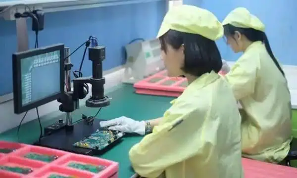
3.1 Manual Visual Inspection (MVI)
How it Works
Manual Visual Inspection (MVI) is the most traditional form of PCB inspection. It involves trained inspectors visually examining PCBs for defects, often with the aid of magnification tools.
Tools Used:
- Magnifying glasses
- Stereo microscopes
- Illuminated magnifiers
- High-resolution cameras with display screens
Pros and Cons
Pros:
- Low initial investment
- Effective for detecting visible surface defects
- Flexible and adaptable to different PCB types
- Can catch unexpected or unusual defects that automated systems might miss
Cons:
- Time-consuming, especially for complex boards
- Subject to human error and fatigue
- Inconsistent results between different inspectors
- Limited effectiveness for small components or hidden defects
Best Practices to Improve Accuracy
- Proper Lighting: Use adjustable, high-quality lighting to enhance visibility of defects.
- Regular Breaks: Implement scheduled breaks to combat eye strain and fatigue.
- Standardized Procedures: Develop and follow consistent inspection checklists and procedures.
- Ongoing Training: Regularly train inspectors on new components and potential defects.
- Ergonomic Workstations: Design inspection areas to minimize physical strain on inspectors.
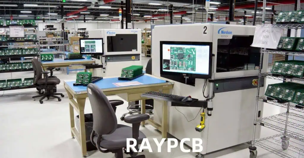
3.2 Automated Optical Inspection (AOI)
Principles of AOI Technology
Automated Optical Inspection uses cameras and image processing software to automatically detect defects on PCBs. It compares captured images of the PCB against a known good board or CAD data to identify anomalies.
Inline vs Offline AOI
- Inline AOI: Integrated directly into the production line, inspecting boards as they move through the manufacturing process.
- Offline AOI: Separate from the production line, used for more detailed inspection or for smaller production runs.
2D vs 3D AOI in 2025: Latest Advances
- 2D AOI: Traditional method, effective for detecting surface-level defects.
- 3D AOI: Uses multiple cameras or laser technology to create a three-dimensional image of the PCB, allowing for more accurate inspection of component height, coplanarity, and solder joint quality.
Latest Advances:
- Higher resolution cameras for detecting smaller defects
- Improved AI algorithms for defect classification
- Integration with factory automation systems for real-time process control
Benefits: Speed, Repeatability, Defect Detection Rates
- Speed: Can inspect hundreds of points per second, much faster than manual inspection.
- Repeatability: Consistent results across multiple inspections and different boards.
- High Defect Detection Rates: Can detect a wide range of defects with high accuracy.
- Data Collection: Provides valuable data for process improvement and traceability.
3.3 X-ray Inspection (AXI)
When and Why to Use X-ray Inspection
X-ray inspection is crucial for examining internal structures of PCBs and components that are not visible to optical inspection methods. It’s particularly useful for:
- Inspecting BGAs (Ball Grid Arrays) and other hidden solder joints
- Checking for voids in solder connections
- Examining multi-layer boards for internal defects
Detecting Hidden Defects
AXI can detect a variety of hidden defects, including:
- Solder bridges under BGA components
- Voids in solder joints
- Misalignment of internal layers in multi-layer PCBs
- Broken internal connections or vias
Differences Between 2D, 2.5D, and 3D X-ray Inspections
- 2D X-ray:
- Provides a top-down view of the PCB
- Useful for basic solder joint inspection
- Limited in detecting issues in overlapping components
- 2.5D X-ray:
- Combines multiple 2D images taken at different angles
- Offers better visibility of solder joints under components
- Improves detection of solder voids and bridges
- 3D X-ray (Computed Tomography):
- Creates a full three-dimensional model of the PCB
- Allows for “slicing” through the board to examine specific layers
- Highest level of defect detection, especially for complex, multi-layer boards
3.4 Flying Probe Testing (FPT)
How Flying Probe Systems Work

Flying Probe Testing uses mobile test probes to make contact with specific points on the PCB, checking for electrical continuity and component values. The probes “fly” from point to point based on the PCB design data.
Ideal Applications: Prototypes, Low-Volume Production
FPT is particularly well-suited for:
- Prototype PCBs where creating a dedicated test fixture isn’t cost-effective
- Low-volume production runs
- Complex boards with dense component placement
- Boards that undergo frequent design changes
Key Advantages:
- No need for expensive, custom test fixtures
- Highly flexible, easily adaptable to different PCB designs
- Can test hard-to-reach points on densely populated boards
3.5 In-Circuit Testing (ICT)
How ICT Differs from Flying Probe Testing
In-Circuit Testing uses a bed-of-nails fixture, a custom-made array of pins that makes contact with specific points on the PCB simultaneously. This allows for faster testing compared to Flying Probe methods.
Strengths in High-Volume Production Environments
ICT excels in high-volume production due to:
- Rapid test execution, often just a few seconds per board
- Comprehensive testing of both passive and active components
- Ability to detect both manufacturing defects and component failures
- High repeatability and consistency in test results
Considerations:
- Requires a custom fixture for each PCB design, which can be costly
- Less flexible than FPT for design changes
- May have limitations for very densely packed boards
3.6 Functional Testing (FCT)

End-Product Functionality Validation
Functional Testing goes beyond checking individual components or connections. It validates that the PCB performs its intended functions as part of the final product.
Where Functional Testing Fits in the Inspection Process
FCT typically occurs after other inspection methods, often as one of the final steps before the PCB is integrated into the end product. It can include:
- Powering up the board and checking for correct voltage levels
- Testing communication interfaces (e.g., USB, Ethernet)
- Verifying sensor inputs and actuator outputs
- Running software-based tests to check overall functionality
Importance:
- Catches issues that might be missed by other inspection methods
- Ensures the PCB will work correctly in its intended application
- Can simulate real-world conditions to test durability and performance
In 2025, a comprehensive PCB inspection strategy often involves a combination of these methods, tailored to the specific requirements of the product, production volume, and quality standards. By leveraging the strengths of each inspection technique, manufacturers can ensure the highest level of quality and reliability in their PCB production.
4. Techniques and Tools for Effective PCB Inspection
As we delve deeper into the world of PCB inspection, it’s crucial to understand the specific techniques and tools used to ensure the quality and reliability of printed circuit boards. In 2025, these methods have become more sophisticated, leveraging advanced technologies to detect even the most minute defects. Let’s explore some of the key techniques and tools used in effective PCB inspection.
4.1 Solder Joint Inspection
Solder joint quality is paramount in PCB manufacturing, as poor solder joints are a common cause of PCB failure. Here are some techniques for identifying various solder joint issues:
Techniques for Identifying Solder Bridges, Voids, and Cold Joints
- Visual Inspection for Solder Bridges:
- Use high-magnification cameras or microscopes to detect unwanted connections between solder points.
- Look for excess solder forming a bridge between adjacent pads or leads.
- X-ray Inspection for Voids:
- Employ X-ray systems to detect voids within solder joints, especially for hidden joints like those in BGAs.
- Analyze X-ray images for dark spots within the solder, indicating air pockets or voids.
- Thermal Imaging for Cold Joints:
- Use infrared cameras to detect temperature differences that may indicate cold solder joints.
- Look for joints that heat up more slowly or to a lower temperature than surrounding joints.
- 3D AOI for Solder Joint Profile:
- Utilize 3D AOI systems to create a three-dimensional model of solder joints.
- Analyze the shape and volume of solder to ensure proper formation an
- Cross-Sectioning for In-Depth Analysis:
- For critical applications or troubleshooting, use physical cross-sectioning of solder joints.
- Examine the internal structure of joints to assess intermetallic compound formation and void distribution.
4.2 Trace and Pad Inspection
Ensuring the integrity of PCB traces and pads is crucial for the overall functionality and reliability of the board. Here are key techniques for this aspect of inspection:
Importance of Checking PCB Traces, Vias, and Pads for Continuity and Quality
- Automated Optical Inspection (AOI) for Surface Traces:
- Use high-resolution cameras to detect breaks, narrowing, or other defects in surface traces.
- Compare against CAD data to ensure trace width and spacing meet design specifications.
- X-ray Inspection for Internal Layers:
- Employ X-ray systems to examine traces and vias in internal layers of multi-layer PCBs.
- Look for disconnections, misalignments, or other defects not visible from the surface.
- Electrical Testing for Continuity:
- Use flying probe or in-circuit testers to verify electrical continuity of traces and vias.
- Check for opens, shorts, and resistance values that fall outside acceptable ranges.
- 3D Profilometry for Pad Height and Coplanarity:
- Utilize laser or structured light 3D scanning to measure pad height and ensure coplanarity.
- Verify that pads meet specifications for subsequent assembly processes like component placement.
- Microsectioning for Via Quality:
- For critical applications, perform microsectioning to examine the internal structure of vias.
- Assess plating thickness, void presence, and overall via formation quality.
4.3 Component Placement and Polarity Verification
Ensuring correct component placement and polarity is essential for PCB functionality. Here are techniques to detect misplaced or rotated components:
How to Detect Misplaced or Rotated Components
- 2D AOI for Component Presence and Position:
- Use pattern matching algorithms to verify component presence and correct positioning.
- Compare component outlines and markings against reference images.
- 3D AOI for Component Height and Coplanarity:
- Employ 3D scanning to measure component height and ensure proper seating on the board.
- Check for tilted or lifted components that may indicate placement issues.
- Fiducial Recognition for Alignment Verification:
- Utilize fiducial markers on the PCB to verify overall alignment accuracy of component placement.
- Ensure components are placed within specified tolerances relative to these reference points.
- Polarity Checking with OCR and Pattern Matching:
- Use Optical Character Recognition (OCR) to read component markings and verify correct orientation.
- Employ pattern matching to check for polarity indicators like diode bands or pin 1 markers.
- X-ray Inspection for Hidden Components:
- Use X-ray systems to verify correct placement and orientation of BGAs and other hidden components.
- Check for proper alignment of internal structures like solder balls or lead frames.
4.4 3D Inspection Technologies
As PCBs become more complex, 3D inspection technologies have become increasingly important. Here’s an overview of the latest advancements:
Use of 3D Profilometry and Laser Measurement in 2025
- Structured Light 3D Scanning:
- Projects a pattern of light onto the PCB surface and analyzes its deformation to create a 3D model.
- Provides high-resolution data on surface topography, component height, and solder joint profiles.
- Laser Triangulation:
- Uses laser line projection and camera imaging to create precise 3D measurements.
- Excellent for measuring component height, coplanarity, and solder paste volume.
- Confocal Microscopy:
- Employs optical sectioning to create high-resolution 3D images of small features.
- Useful for inspecting fine-pitch components and analyzing surface textures.
- Multi-Angle and Multi-Spectral Imaging:
- Combines images from multiple angles and light spectra to create comprehensive 3D models.
- Enhances defect detection capabilities, especially for complex geometries and varied materials.
- AI-Enhanced 3D Analysis:
- Utilizes machine learning algorithms to interpret 3D scan data and identify defects.
- Improves detection accuracy and reduces false positives in 3D inspection processes.
These advanced 3D inspection technologies allow for more precise measurements and better detection of defects related to component placement, solder joint quality, and overall board topology. They are particularly valuable for inspecting complex, densely populated PCBs and for ensuring compliance with increasingly stringent manufacturing standards.
By employing these techniques and tools, PCB manufacturers can significantly enhance their inspection capabilities, ensuring higher quality products and reducing the risk of field failures. As we move further into 2025 and beyond, we can expect these technologies to become even more sophisticated, with increased integration of AI and machine learning to further improve defect detection and process control in PCB manufacturing.
5. Common PCB Defects Found During Inspection
As PCB designs become more complex and manufacturing processes more advanced, the types of defects that can occur during production have also evolved. In 2025, PCB inspection processes are designed to catch a wide array of potential issues. Understanding these common defects is crucial for maintaining high-quality standards in PCB manufacturing. Let’s explore the main categories of defects typically found during PCB inspection:
Soldering Issues: Bridges, Voids, Insufficient Solder
- Solder Bridges:
- Description: Unwanted connections between two or more solder points.
- Causes: Excessive solder, component misalignment, or incorrect stencil design.
- Detection: Visual inspection, AOI, X-ray for hidden bridges.
- Solder Voids:
- Description: Air pockets or gaps within a solder joint.
- Causes: Outgassing during reflow, contamination, or improper solder paste application.
- Detection: X-ray inspection, especially for BGA and hidden joints.
- Insufficient Solder:
- Description: Not enough solder to form a proper connection.
- Causes: Inadequate solder paste, poor wetting, or component misalignment.
- Detection: AOI, X-ray, and visual inspection.
- Cold Solder Joints:
- Description: Joints where the solder hasn’t properly bonded to the pad or component lead.
- Causes: Insufficient heat during soldering, contamination, or oxidation.
- Detection: Visual inspection, thermal imaging, and electrical testing.
Component Defects: Missing, Wrong Polarity, Wrong Part
- Missing Components:
- Description: Components that are absent from their designated locations.
- Causes: Pick-and-place machine errors, component shortages, or human error in manual assembly.
- Detection: AOI, visual inspection, and electrical testing.
- Incorrect Polarity:
- Description: Components placed in the wrong orientation.
- Causes: Programming errors in pick-and-place machines or human error.
- Detection: AOI with pattern matching, visual inspection, and functional testing.
- Wrong Component:
- Description: Incorrect component type or value placed on the board.
- Causes: Mis-loaded feeders, inventory mix-ups, or incorrect programming.
- Detection: AOI with OCR capabilities, X-ray for package verification, and electrical testing.
- Component Misalignment:
- Description: Components that are slightly off their intended position or tilted.
- Causes: Pick-and-place machine calibration issues or component warpage.
- Detection: AOI, especially 3D AOI for detecting subtle misalignments.
PCB Substrate Problems: Cracks, Delamination
- Cracks in the PCB:
- Description: Fractures in the PCB substrate.
- Causes: Thermal stress, physical impact, or manufacturing defects.
- Detection: Visual inspection, X-ray for internal cracks, and stress testing.
- Delamination:
- Description: Separation of PCB layers.
- Causes: Moisture ingress, thermal stress, or manufacturing defects.
- Detection: Acoustic microscopy, X-ray inspection, and thermal stress testing.
- Warpage:
- Description: Bending or twisting of the PCB.
- Causes: Uneven cooling, thermal mismatch, or internal stresses.
- Detection: 3D profilometry, visual inspection, and flatness testing.
Electrical Defects: Shorts, Opens, Leakage

- Short Circuits:
- Description: Unintended connections between circuit points.
- Causes: Solder bridges, conductive contamination, or design errors.
- Detection: In-circuit testing, flying probe testing, and power-on testing.
- Open Circuits:
- Description: Breaks in intended electrical pathways.
- Causes: Broken traces, lifted pads, or incomplete solder joints.
- Detection: Electrical continuity testing, flying probe testing, and functional testing.
- High Resistance Connections:
- Description: Connections with higher than expected resistance.
- Causes: Poor soldering, oxidation, or partial breaks in traces.
- Detection: Precision resistance measurement, thermal imaging during power-on.
- Leakage Currents:
- Description: Unintended current flow between isolated circuit sections.
- Causes: Contamination, moisture ingress, or insulation breakdown.
- Detection: Insulation resistance testing, specialized leakage current tests.
Additional Common Defects
- Solder Paste Issues:
- Insufficient or excess solder paste
- Smeared or misaligned solder paste deposits
- Detection: Solder paste inspection (SPI) systems
- Via Defects:
- Incomplete plating
- Voids in via fill
- Detection: X-ray inspection, microsectioning for critical applications
- Pad Lift-Off:
- Description: Separation of copper pads from the PCB substrate
- Causes: Excessive heat during rework, poor adhesion in manufacturing
- Detection: Visual inspection, stress testing
- Tombstoning:
- Description: One end of a component lifts off the pad during soldering
- Causes: Uneven heating, pad design issues, or component placement problems
- Detection: AOI, visual inspection
- Foreign Object Debris (FOD):
- Description: Unwanted particles or objects on the PCB
- Causes: Contamination during manufacturing or handling
- Detection: Visual inspection, AOI
Understanding these common defects is crucial for developing effective inspection strategies and improving overall PCB quality. In 2025, the integration of AI and machine learning into inspection systems is enhancing the ability to detect and classify these defects accurately and efficiently. This not only improves the quality of individual PCBs but also provides valuable data for continuous improvement of the manufacturing process.
6. Best Practices for PCB Inspection in 2025
As we navigate the complexities of PCB manufacturing in 2025, implementing best practices in inspection processes is crucial for ensuring high-quality, reliable products. These practices not only help in detecting defects but also in preventing them and optimizing the overall manufacturing process. Let’s explore the key best practices for PCB inspection:
Design for Inspection (DFI): Designing PCBs with Inspection in Mind
- Incorporate Test Points:
- Include dedicated test points in PCB designs to facilitate easier electrical testing.
- Ensure test points are accessible for both automated and manual inspection methods.
- Optimize Component Placement:
- Design layouts that allow for clear visual access to components and solder joints.
- Avoid placing small components under larger ones where possible.
- Use Fiducial Markers:
- Include fiducial markers to aid in alignment during automated inspection processes.
- Place fiducials strategically for maximum effectiveness in component placement verification.
- Consider X-ray Inspection Requirements:
- For boards with BGAs or other hidden solder joints, design with X-ray inspection in mind.
- Avoid overlapping components that could obscure X-ray views of critical areas.
- Standardize Pad Designs:
- Use consistent pad designs where possible to simplify automated inspection programming.
- Ensure pad sizes and shapes are optimized for both soldering and inspection processes.
Choosing the Right Inspection Method Based on Volume, Complexity, and Cost
- Assess Production Volume:
- For high-volume production, invest in automated systems like AOI and AXI.
- For low-volume or prototype runs, consider more flexible options like flying probe testing.
- Evaluate Board Complexity:
- For complex, multi-layer boards, incorporate X-ray inspection into the process.
- Use 3D AOI for boards with a high mix of component types and sizes.
- Consider Cost-Effectiveness:
- Balance the cost of inspection equipment against the potential cost of field failures.
- Factor in the long-term benefits of data collection and process improvement capabilities.
- Adapt to Product Lifecycle:
- Implement more rigorous inspection processes during new product introduction phases.
- Adjust inspection strategies as products mature and processes stabilize.
Combining Multiple Inspection Methods for Maximum Reliability
- Implement a Multi-Stage Inspection Process:
- Use SPI (Solder Paste Inspection) before component placement.
- Follow with AOI after placement and reflow.
- Incorporate AXI for critical or hidden joints.
- Finish with ICT or functional testing.
- Tailor Inspection Combinations to Product Requirements:
- For high-reliability products (e.g., medical, aerospace), use a combination of visual, AOI, AXI, and electrical testing.
- For consumer electronics, balance speed and cost with an appropriate mix of automated and sampling-based inspections.
- Use Data Integration:
- Implement systems that allow data sharing between different inspection stages.
- Utilize this integrated data for comprehensive defect analysis and process improvement.
Training and Certification for Inspection Personnel
- Develop Comprehensive Training Programs:
- Provide in-depth training on PCB technology, common defects, and inspection equipment.
- Include hands-on practice with a variety of PCB types and potential defects.
- Pursue Industry Certifications:
- Encourage staff to obtain relevant certifications (e.g., IPC Certification).
- Support ongoing education to keep up with evolving technologies and standards.
- Implement Regular Skill Assessments:
- Conduct periodic evaluations of inspector performance and knowledge.
- Use results to tailor ongoing training and development programs.
- Foster a Culture of Continuous Learning:
- Encourage knowledge sharing among team members.
- Provide opportunities for inspectors to learn about new technologies and industry trends.
Maintaining and Calibrating Inspection Equipment
- Establish Regular Calibration Schedules:
- Develop and adhere to calibration schedules for all inspection equipment.
- Use traceable standards for calibration processes.
- Perform Routine Maintenance:
- Implement preventive maintenance programs for all inspection systems.
- Keep detailed maintenance logs and track equipment performance over time.
- Verify Equipment Accuracy:
- Regularly use known good boards and known defect boards to verify inspection system performance.
- Adjust and fine-tune systems as needed based on these verifications.
- Stay Current with Software Updates:
- Keep inspection system software up-to-date to benefit from the latest algorithms and features.
- Evaluate and implement new software capabilities that can enhance inspection accuracy or efficiency.
- Monitor Environmental Conditions:
- Ensure inspection areas maintain stable temperature and humidity levels.
- Use environmental monitoring systems to track and log conditions that could affect inspection accuracy.
Implementing Continuous Improvement Processes
- Analyze Inspection Data:
- Regularly review data from all inspection stages to identify trends and recurring issues.
- Use statistical process control (SPC) methods to monitor and improve manufacturing processes.
- Conduct Root Cause Analysis:
- For significant or recurring defects, perform thorough root cause analysis.
- Implement corrective actions based on these analyses to prevent future occurrences.
- Foster Collaboration Between Departments:
- Encourage regular meetings between design, manufacturing, and quality control teams.
- Use inspection findings to inform design improvements and manufacturing process adjustments.
- Benchmark Against Industry Standards:
- Regularly compare your inspection processes and results against industry benchmarks.
- Participate in industry forums and associations to stay informed about best practices.
- Invest in New Technologies:
- Stay informed about advancements in inspection technologies.
- Evaluate and implement new technologies that can improve inspection accuracy or efficiency.
7. Trends Shaping the Future of PCB Inspection
As we look towards the future of PCB inspection, several key trends are emerging that promise to revolutionize the field. These advancements are not only improving the accuracy and efficiency of inspection processes but also transforming how manufacturers approach quality control in PCB production. Let’s explore the major trends shaping the future of PCB inspection in 2025 and beyond.
AI and Machine Learning in Automated Inspections
Artificial Intelligence (AI) and Machine Learning (ML) are rapidly becoming integral parts of PCB inspection systems, offering unprecedented levels of accuracy and efficiency.
- Advanced Defect Detection:
- AI algorithms can identify complex defect patterns that might be missed by traditional rule-based systems.
- Machine learning models continually improve their detection capabilities as they process more data.
- Adaptive Inspection Parameters:
- AI systems can automatically adjust inspection parameters based on board type, component density, and historical data.
- This adaptability reduces the need for manual programming and improves inspection accuracy across diverse product lines.
- Anomaly Detection:
- ML algorithms excel at identifying unusual patterns or defects that don’t fit known categories.
- This capability is particularly valuable for detecting new or rare defect types.
- Predictive Maintenance:
- AI can analyze inspection system performance data to predict maintenance needs, reducing downtime.
- This proactive approach ensures consistent inspection quality and extends equipment lifespan.
- Real-time Process Optimization:
- AI systems can analyze inspection data in real-time to suggest process adjustments, reducing defect rates on the fly.
Integration of PCB Inspection into Smart Manufacturing (Industry 4.0)
The concept of Industry 4.0 is transforming PCB manufacturing, with inspection playing a crucial role in this digital transformation.
- Connected Inspection Systems:
- Inspection equipment is increasingly integrated with other manufacturing systems, allowing for seamless data exchange.
- This connectivity enables real-time monitoring and control of the entire production process.
- Digital Twin Technology:
- Virtual models (digital twins) of PCBs and manufacturing processes are used to simulate and optimize inspection strategies.
- These models can predict potential defects and guide targeted inspection efforts.
- Cloud-Based Data Management:
- Inspection data is stored and analyzed in cloud platforms, allowing for global access and advanced analytics.
- This centralized approach facilitates better collaboration and decision-making across multiple manufacturing sites.
- IoT Sensors for Environmental Monitoring:
- Internet of Things (IoT) sensors monitor environmental conditions that could affect PCB quality or inspection accuracy.
- Real-time data from these sensors can trigger automatic adjustments in manufacturing or inspection processes.
- Augmented Reality in Manual Inspections:
- AR technologies assist human inspectors by overlaying digital information onto physical PCBs.
- This can guide inspectors to potential problem areas and provide real-time reference information.
Predictive Analytics to Anticipate Failure Points Before They Occur
Predictive analytics is moving PCB inspection from a reactive to a proactive approach, helping manufacturers identify potential issues before they become actual defects.
- Early Warning Systems:
- Advanced analytics models analyze historical and real-time data to predict potential defects or process deviations.
- These systems can alert operators to take preventive action before quality issues occur.
- Lifecycle Prediction:
- Predictive models can estimate the expected lifespan and reliability of PCBs based on inspection data and usage patterns.
- This information is valuable for both manufacturers and end-users in planning maintenance and replacements.
- Supply Chain Integration:
- Predictive analytics extend beyond the production floor, integrating data from suppliers to anticipate quality issues related to raw materials or components.
- Customer Usage Insights:
- Analysis of field data and customer usage patterns can inform inspection criteria, focusing efforts on areas most likely to impact real-world performance.
- Continuous Process Improvement:
- Predictive models identify subtle trends and correlations in manufacturing data, driving continuous refinement of processes and inspection methods.
Eco-Friendly Inspection Methods and Materials
Environmental considerations are becoming increasingly important in PCB manufacturing and inspection.
- Energy-Efficient Inspection Systems:
- New inspection technologies are designed with energy efficiency in mind, reducing the carbon footprint of quality control processes.
- Reduced Use of Harmful Chemicals:
- Inspection methods that reduce or eliminate the need for chemical cleaning or processing are gaining popularity.
- Non-Destructive Testing Advancements:
- Improvements in non-destructive testing methods reduce waste associated with destructive testing practices.
- Recyclable and Biodegradable Materials:
- Development of PCB materials that are more easily recyclable or biodegradable, with inspection processes adapted to these new materials.
- Water Conservation in Cleaning Processes:
- Inspection technologies that reduce the need for water-based cleaning, or that use water more efficiently in necessary cleaning processes.
Miniaturization and Increased Density Challenges
As PCBs continue to shrink while becoming more complex, inspection technologies are evolving to meet these challenges.
- High-Resolution Imaging:
- Development of ultra-high-resolution cameras and optics to inspect increasingly miniature components and features.
- Advanced X-ray Technologies:
- Improvements in X-ray resolution and 3D reconstruction capabilities to inspect dense, multi-layer boards.
- Nano-scale Inspection Techniques:
- Emerging technologies for inspecting nano-scale features and components on advanced PCBs.
- Multi-sensor Fusion:
- Combining data from multiple sensor types (optical, X-ray, thermal, etc.) to create more comprehensive inspection results.
- AI-Enhanced Image Processing:
- Using AI to extract meaningful information from complex, high-resolution inspection images of densely packed PCBs.
These trends are not just theoretical concepts but are actively shaping the landscape of PCB inspection in 2025. Manufacturers who embrace these technologies and approaches will be well-positioned to produce higher quality PCBs, reduce defects, and meet the ever-increasing demands of the electronics industry. As these trends continue to evolve, we can expect even more innovative solutions to emerge, further advancing the field of PCB inspection and quality control.
8. How to Choose the Right PCB Inspection Strategy
Selecting the appropriate PCB inspection strategy is crucial for ensuring product quality while maintaining efficiency and cost-effectiveness. In 2025, with a wide array of inspection technologies and methodologies available, making the right choice can be complex. This section will guide you through the key factors to consider and provide a framework for decision-making.
Factors to Consider: Production Volume, Complexity, Budget, Compliance Needs
- Production Volume:
- High Volume: Favor automated systems like AOI and AXI for speed and consistency.
- Low Volume: Consider more flexible options like manual inspection or flying probe testing.
- Mixed Production: Look for adaptable systems that can handle varying batch sizes efficiently.
- PCB Complexity:
- Simple Boards: Basic visual inspection and 2D AOI may be sufficient.
- Complex Multi-layer Boards: Incorporate X-ray inspection and 3D AOI.
- High-Density Boards: Consider advanced optical and X-ray technologies with high resolution capabilities.
- Budget Constraints:
- Initial Investment: Balance upfront costs with long-term savings from improved quality and reduced rework.
- Operational Costs: Consider ongoing expenses like maintenance, training, and potential upgrades.
- Return on Investment: Evaluate how quickly inspection systems will pay for themselves through defect reduction and improved efficiency.
- Compliance Requirements:
- Industry-Specific Standards: Ensure inspection methods meet relevant standards (e.g., IPC, ISO, AS9100 for aerospace).
- Traceability Needs: Choose systems that provide detailed documentation and data logging if required for compliance.
- Customer Requirements: Consider any specific inspection criteria mandated by key customers.
- Product Lifecycle Stage:
- New Product Introduction: Implement more rigorous inspection processes during early production phases.
- Mature Products: Adjust inspection strategies as processes stabilize and defect patterns become well-understood.
- Manufacturing Environment:
- Clean Room Requirements: Choose inspection equipment compatible with clean room standards if applicable.
- Space Constraints: Consider the physical footprint of inspection systems in your facility layout.
- Integration with Existing Systems: Evaluate how new inspection tools will integrate with current manufacturing and data systems.
- Defect Types and Detection Needs:
- Common Defects: Prioritize inspection methods that excel at detecting your most frequent or critical defect types.
- Hidden Defects: Include X-ray inspection if internal defects are a concern (e.g., for BGA or multi-layer boards).
- Speed and Throughput Requirements:
- Production Line Speed: Ensure inspection methods can keep pace with your manufacturing line.
- Batch Processing vs. Inline Inspection: Determine whether offline batch inspection or inline continuous inspection is more suitable.
Decision Tree or Simple Table to Guide Selection
To help guide your decision-making process, consider the following simplified decision tree:
- Determine Production Volume:
- High Volume (>1000 boards/day) → Go to 2
- Medium Volume (100-1000 boards/day) → Go to 3
- Low Volume (<100 boards/day) → Go to 4
- High Volume Production:
- Complex Multi-layer Boards → Combine AOI, AXI, and ICT
- Simple to Moderate Complexity → AOI and ICT
- High-Reliability Requirements → Add Functional Testing
- Medium Volume Production:
- Complex Boards → 3D AOI and Sample-based AXI
- Moderate Complexity → 2D or 3D AOI
- Frequent Design Changes → Include Flying Probe Testing
- Low Volume Production:
- Prototype or Frequent Changes → Manual Inspection and Flying Probe
- Stable Design, High Complexity → AOI and Sample-based X-ray
- Simple Boards → Manual Inspection with Assistance Tools
Here’s a simple table to further guide your selection based on key factors:
| Factor | Recommended Inspection Methods |
|---|---|
| High Volume | AOI, AXI, ICT |
| Low Volume | Manual Inspection, Flying Probe, Functional Testing |
| High Complexity | 3D AOI, AXI, CT Scanning |
| Simple Boards | 2D AOI, Manual Inspection |
| Hidden Joints (BGAs) | X-ray Inspection (2D or 3D) |
| Frequent Changes | Flying Probe, Flexible AOI Systems |
| High Reliability Needs | Combination of AOI, AXI, ICT, and Functional Testing |
| Budget Constraints | Prioritize Critical Areas, Consider Outsourcing |
| Compliance-Driven | Systems with Strong Data Logging and Traceability |
Remember, the ideal inspection strategy often involves a combination of methods, tailored to your specific needs. It’s also important to regularly review and adjust your inspection strategy as technology advances and your production needs evolve.
By carefully considering these factors and using the decision tree and table as guides, you can develop a PCB inspection strategy that balances quality, efficiency, and cost-effectiveness for your specific manufacturing context in 2025 and beyond.
Conclusion
As we’ve explored throughout this comprehensive guide, PCB inspection plays a crucial role in ensuring the quality, reliability, and performance of electronic products in 2025 and beyond. The landscape of PCB manufacturing and inspection continues to evolve rapidly, driven by technological advancements, increasing product complexity, and ever-higher quality standards.
Let’s recap the key points we’ve covered:
- The Critical Importance of PCB Inspection: We’ve seen how thorough inspection processes are essential for detecting defects early, reducing costs, and ensuring product reliability across various industries.
- Diverse Inspection Methods: From traditional visual inspection to advanced automated systems like AOI, AXI, and 3D scanning technologies, a wide range of tools and techniques are available to address different inspection needs.
- Common Defects and Detection Techniques: Understanding the types of defects that can occur in PCBs and the most effective methods for detecting them is crucial for implementing a robust inspection strategy.
- Best Practices: We’ve outlined key practices such as designing for inspection, combining multiple inspection methods, and maintaining and calibrating equipment to optimize the inspection process.
- Emerging Trends: The integration of AI and machine learning, the move towards smart manufacturing, and the use of predictive analytics are shaping the future of PCB inspection, offering new possibilities for accuracy and efficiency.
- Strategic Decision-Making: Choosing the right inspection strategy involves carefully considering factors such as production volume, board complexity, budget constraints, and compliance requirements.
As we look to the future, several key trends will continue to shape PCB inspection:
- Increasing Automation and AI Integration: The role of artificial intelligence in defect detection and process optimization will grow, leading to more accurate and efficient inspection processes.
- Greater Connectivity and Data Integration: In line with Industry 4.0 principles, PCB inspection will become more integrated with other manufacturing processes, enabling real-time adjustments and improvements.
- Advancements in Miniaturization: As PCBs continue to shrink and become more complex, inspection technologies will need to evolve to handle increasingly fine details and dense layouts.
- Focus on Sustainability: Eco-friendly inspection methods and materials will gain importance as the industry strives for greater environmental responsibility.
For manufacturers and engineers looking to optimize their inspection processes in 2025 and beyond, here are some final tips:
- Stay Informed: Keep abreast of the latest developments in PCB inspection technologies and methodologies. Attend industry conferences, participate in webinars, and engage with technology providers to understand new capabilities.
- Invest in Training: Ensure that your team is well-trained not only in operating inspection equipment but also in understanding the principles behind different inspection methods and interpreting results accurately.
- Embrace Data-Driven Decision Making: Utilize the wealth of data generated by modern inspection systems to drive continuous improvement in your manufacturing processes.
- Be Flexible and Adaptable: As product requirements and technologies change, be prepared to adjust your inspection strategies accordingly. Regular reviews of your inspection processes can help ensure they remain effective and efficient.
- Collaborate Across Departments: Foster strong communication between design, manufacturing, and quality control teams. Insights from inspection processes can inform better design practices and manufacturing techniques.
- Consider Total Cost of Ownership: When investing in new inspection technologies, look beyond the initial price tag to consider factors like efficiency gains, reduced scrap rates, and improved product quality over time.
- Prioritize Traceability: Implement robust systems for tracking and documenting inspection results, which is increasingly important for regulatory compliance and customer satisfaction.
In conclusion, as PCBs continue to play a central role in our increasingly electronic world, the importance of effective inspection cannot be overstated. By leveraging the latest technologies, adhering to best practices, and maintaining a commitment to quality, manufacturers can ensure that their PCBs meet the high standards required in 2025 and beyond. The future of PCB inspection is one of greater precision, efficiency, and integration, promising exciting possibilities for the entire electronics industry.
FAQs
- What are the most common PCB inspection methods? The most common PCB inspection methods include Automated Optical Inspection (AOI), X-ray Inspection (AXI), In-Circuit Testing (ICT), Flying Probe Testing, and Manual Visual Inspection. Each method has its strengths and is often used in combination with others for comprehensive quality control.
- What is the difference between AOI and AXI inspection? AOI (Automated Optical Inspection) uses cameras and image processing to inspect the surface of PCBs, detecting visible defects like component placement issues or solder problems. AXI (Automated X-ray Inspection) uses X-rays to inspect internal aspects of the PCB, particularly useful for detecting defects in hidden solder joints, like those in BGAs or multi-layer boards.
- Can AI improve PCB inspection accuracy? Yes, AI can significantly improve PCB inspection accuracy. Machine learning algorithms can be trained to detect subtle defects that might be missed by traditional inspection methods. AI can also adapt to new defect types, reduce false positives, and improve overall inspection efficiency.