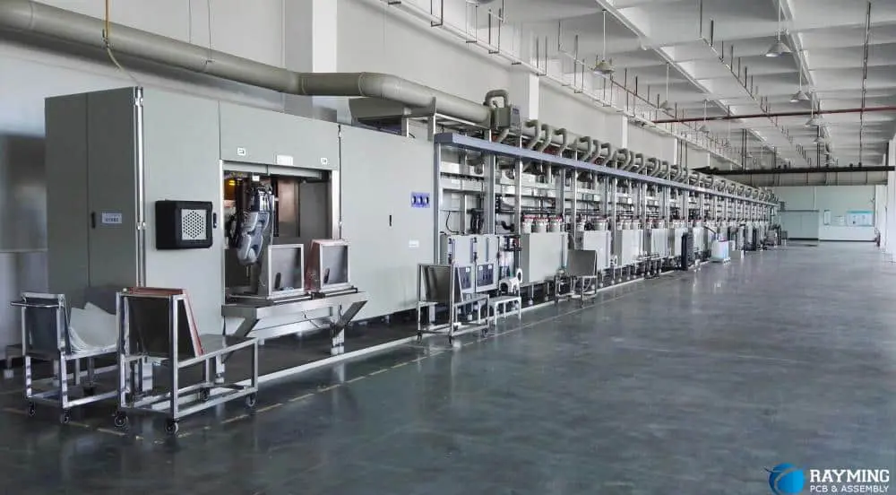
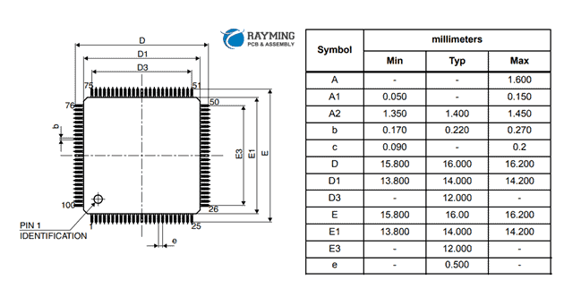
China dominates the global PCB (Printed Circuit Board) manufacturing industry, producing over 50% of the world’s PCBs . As the backbone of modern electronics, PCBs are essential in everything from consumer gadgets to aerospace systems. For businesses seeking high-quality, cost-effective, and fast-turnaround PCB solutions, China remains the top destination.
At [Your Company Name], we are a leading China PCB manufacturer, specializing in PCB fabrication, assembly, and prototyping with ISO-certified quality, competitive pricing, and rapid delivery. Whether you need prototypes, multilayer PCBs, HDI boards, or full turnkey assembly, we provide end-to-end solutions tailored to your needs.
A: Check ISO 9001, IPC-A-600, and RoHS certifications .
Q3: Which city in China is best for PCB manufacturing?
A: Shenzhen (80% of China’s PCB factories are here) .
Q4: Can I get assembled PCBs from China?
A: Yes! Turnkey PCBA services include SMT, testing, and packaging .
Conclusion
Choosing the right China PCB manufacturer ensures high-quality, affordable, and fast electronic production. Whether you need prototypes, HDI boards, or mass production, [Your Company Name] provides end-to-end PCB solutions with 24/7 support.
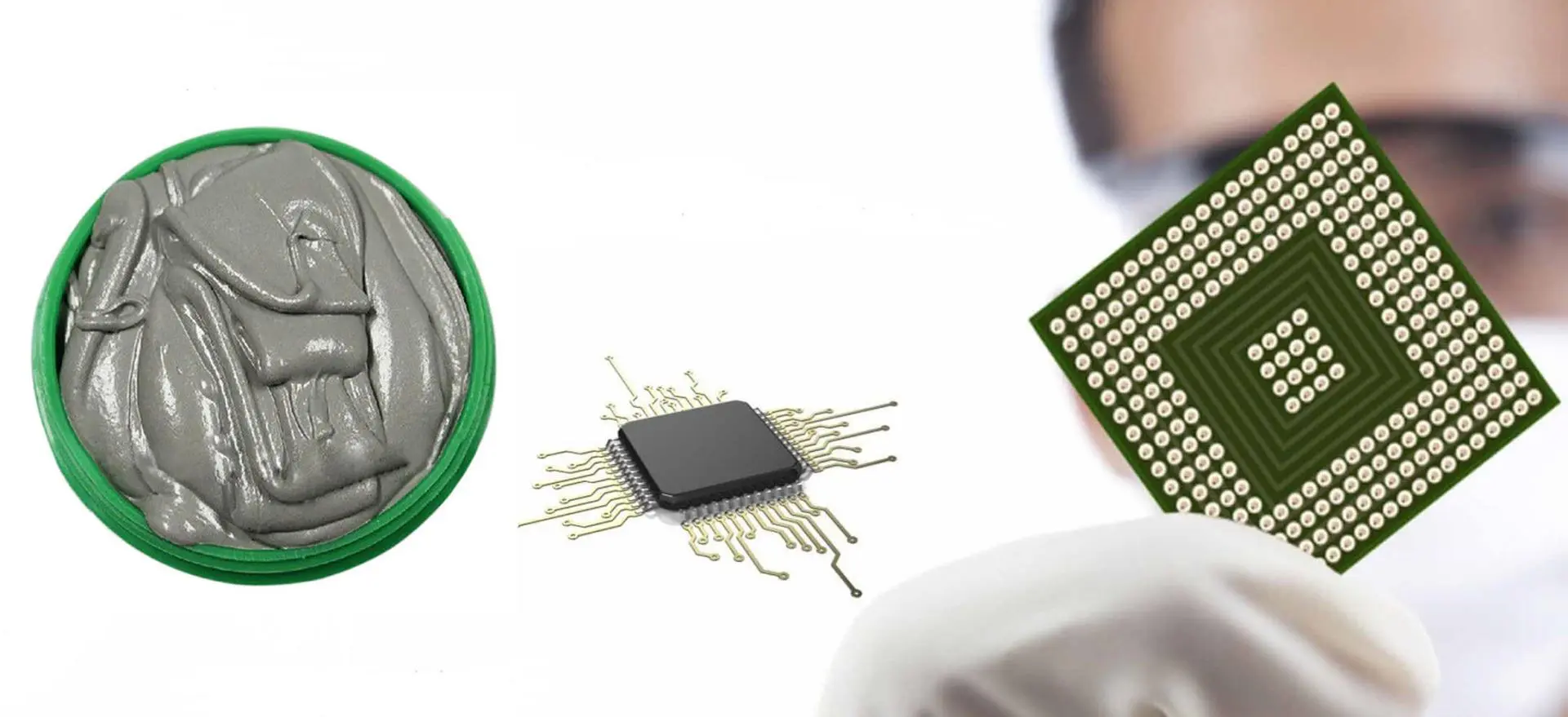
In the world of electronics manufacturing, solder paste plays a crucial role in creating reliable connections between components and printed circuit boards (PCBs). This guide will provide a comprehensive overview of solder paste, its types, applications, and best practices for PCB assembly.
What is Solder Paste?
Solder paste is a specially formulated material used in the electronics industry for soldering components to PCBs. It consists of tiny metal particles suspended in a flux medium, creating a paste-like consistency. This unique composition allows for precise application and excellent electrical conductivity when melted.
Is Solder Paste and Flux the Same?
While solder paste contains flux, they are not the same thing. Flux is a chemical cleaning agent that helps remove oxides from metal surfaces, promoting better adhesion and electrical connections. Solder paste, on the other hand, combines flux with metal particles to create a complete soldering solution.
Do You Need Solder Paste to Solder?
Solder paste is not always necessary for soldering, but it offers significant advantages in many applications, especially in surface-mount technology (SMT) assembly. For through-hole components or manual soldering, traditional wire solder can be used. However, solder paste is essential for automated PCB assembly processes and provides superior results in terms of consistency and reliability.
Composition & Types of Solder Paste
Understanding the composition and various types of solder paste is crucial for selecting the right product for your specific application.
What is Solder Paste Made Of?
Solder paste typically consists of two main components:
Metal alloy particles: These are tiny spheres of metal alloy, usually a combination of tin, lead (in some cases), silver, and copper.
Flux: A sticky substance that helps clean the metal surfaces and promote better bonding.
The metal particles make up about 85-90% of the paste by weight, while the flux accounts for the remaining 10-15%.
How to Make Solder Paste?
While it’s possible to make solder paste at home, it’s generally not recommended for professional applications due to the need for precise composition and consistency. Commercial solder paste is manufactured using specialized equipment and processes, including:
Alloying: Creating the metal alloy with the desired composition.
Atomization: Converting the molten alloy into tiny spherical particles.
Sieving: Sorting the particles by size to ensure uniformity.
Mixing: Combining the metal particles with the flux medium.
Packaging: Storing the paste in syringes or jars for easy application.
Solder Paste Grades Explained
Solder paste is classified into different grades based on the size of the metal particles:
Type 1: 150-75 μm (rarely used in modern electronics)
Type 2: 75-45 μm (used for some through-hole applications)
Type 3: 45-25 μm (common for general SMT applications)
Type 4: 38-20 μm (for fine-pitch components)
Type 5: 25-15 μm (for ultra-fine pitch applications)
Type 6: 15-5 μm (for extremely fine pitch or specialized applications)
The smaller the particle size, the finer the pitch of components that can be soldered.
Common Solder Paste Types
Several types of solder paste are available, each with its own characteristics:
Leaded solder paste: Contains lead and tin (e.g., 63/37 Sn/Pb)
Lead-free solder paste: Typically contains tin, silver, and copper (SAC alloys)
No-clean solder paste: Leaves minimal residue, eliminating the need for post-reflow cleaning
Water-soluble solder paste: Residues can be cleaned with water after reflow
Rosin-based solder paste: Contains natural or synthetic rosin flux
Understanding the properties and benefits of solder paste is essential for optimizing your PCB assembly process.
Key Properties of Solder Paste
Viscosity: Affects the paste’s ability to be dispensed and maintain its shape
Tackiness: Determines how well components stick to the paste before reflow
Slump resistance: Prevents the paste from spreading or moving after application
Printability: Ease of application through stencil printing
Wetting ability: How well the molten solder spreads on the surfaces
Shelf life: Duration the paste remains usable when properly stored
Working life: Time the paste remains effective after being removed from storage
Solder Paste Features & Benefits
Precise component placement: Allows for accurate positioning of SMT components
Uniform solder joints: Creates consistent and reliable electrical connections
Flux integration: Built-in flux eliminates the need for separate flux application
Compatibility with automation: Ideal for use in high-volume production environments
Reduced bridging: Helps prevent solder bridges between closely spaced leads
Improved thermal management: Helps dissipate heat from components
Customizable alloys: Available in various compositions to suit specific requirements
Applications & How to Use Solder Paste
Solder paste is widely used in electronics manufacturing, particularly in SMT assembly processes. Understanding its application methods and differences from other materials is crucial for successful PCB production.
How is Solder Paste Applied to PCBs?
There are two main methods for applying solder paste to PCBs:
Stencil printing: The most common method for high-volume production
A metal stencil with apertures is placed over the PCB
Solder paste is spread across the stencil using a squeegee
The stencil is removed, leaving precise deposits of paste on the PCB pads
Dispensing: Used for prototyping, rework, or low-volume production
Solder paste is dispensed through a syringe or pneumatic system
Allows for more flexibility but is slower than stencil printing
How to Manually Apply Solder Paste
For small-scale projects or prototyping, manual application of solder paste can be done using the following steps:
Clean the PCB surface thoroughly
Use a syringe or dispenser to apply small amounts of paste to each pad
Ensure consistent volume and placement of paste deposits
Place components carefully onto the paste deposits
When working with solder paste on a small scale, a heat gun can be used for reflow:
Apply solder paste and place components as described above
Set the heat gun to the appropriate temperature (usually around 350°C-400°C)
Move the heat gun in a circular motion over the PCB, maintaining a consistent distance
Observe the solder paste as it melts and forms joints
Allow the board to cool slowly to avoid thermal shock
Solder Paste vs. Solder Mask
It’s important to understand the difference between solder paste and solder mask:
Solder paste: A mixture of flux and metal particles used for creating electrical connections
Solder mask: A thin layer of polymer applied to the PCB to protect copper traces and prevent solder bridges
While both are used in PCB assembly, they serve different purposes and should not be confused.
Best Practices for Solder Paste Handling
Proper handling and storage of solder paste are critical for maintaining its effectiveness and ensuring high-quality results in PCB assembly.
Solder Paste Storage Tips
Temperature control: Store solder paste at the manufacturer’s recommended temperature, typically between 0°C and 10°C
Sealed containers: Keep unused paste in airtight containers to prevent contamination and drying
Avoid condensation: Allow paste to reach room temperature before opening to prevent moisture absorption
Rotate stock: Use older paste first to ensure freshness
Follow expiration dates: Discard paste that has exceeded its shelf life
Thawing Time of Solder Paste
Proper thawing of refrigerated solder paste is crucial:
Remove the paste from refrigeration and allow it to reach room temperature
Typical thawing time is 3-4 hours for a 500g jar
Avoid using artificial heat sources to speed up the process
Gently mix the paste after thawing to ensure uniform consistency
How Long Can Solder Paste Sit Before Reflow?
The working life of solder paste on a PCB before reflow varies depending on the paste type and environmental conditions:
Typical working life ranges from 8 to 24 hours
Factors affecting working life include humidity, temperature, and exposure to air
Always follow the manufacturer’s recommendations
For best results, aim to complete reflow as soon as possible after paste application
The 5-Ball Rule for Solder Paste
The 5-ball rule is a quick visual test to assess solder paste quality:
Dispense five small, equally-sized balls of solder paste onto a clean surface
Observe the balls for 10-15 minutes at room temperature
If the balls maintain their shape and don’t slump or spread, the paste is likely suitable for use
If the balls flatten or merge, the paste may have degraded and should be tested further or replaced
Quality Control & Inspection
Maintaining high standards in solder paste application is crucial for producing reliable PCBs. Regular inspection and quality control measures help identify and prevent potential issues.
Cause: Inadequate paste volume or poor stencil design
Prevention: Optimize stencil aperture size and ensure proper stencil cleaning
Solder bridges:
Cause: Excessive paste, poor pad design, or improper stencil removal
Prevention: Adjust paste volume, improve pad design, and ensure careful stencil handling
Solder balls:
Cause: Excessive flux or improper reflow profile
Prevention: Use appropriate flux content and optimize reflow temperature profile
Cold solder joints:
Cause: Insufficient heat during reflow or contaminated surfaces
Prevention: Ensure proper reflow temperature and clean PCB surfaces
Tombstoning:
Cause: Uneven heating or paste application
Prevention: Balance paste deposits and optimize component placement
Voiding:
Cause: Entrapped gases or improper flux activation
Prevention: Use low-voiding solder pastes and optimize reflow profile
By implementing rigorous quality control measures and addressing these common defects, manufacturers can significantly improve the reliability and performance of their PCB assemblies.
Conclusion
Summary of Key Takeaways
Solder paste is a critical component in modern electronics manufacturing, particularly in SMT assembly processes. Its unique composition of metal alloy particles suspended in flux allows for precise application and reliable electrical connections. Key points to remember include:
Solder paste comes in various grades and types, each suited for specific applications
Proper storage, handling, and application techniques are essential for optimal results
Quality control measures, such as SPI and defect prevention strategies, are crucial for producing high-quality PCBs
Understanding the properties and benefits of solder paste helps in selecting the right product for your needs
Future Trends in Solder Paste Technology
As electronics continue to evolve, solder paste technology is also advancing to meet new challenges:
Development of lead-free alloys with improved performance characteristics
Nano-sized particle solder pastes for ultra-fine pitch applications
Low-temperature solder pastes for temperature-sensitive components
Increased focus on environmentally friendly and sustainable solder paste formulations
Integration of smart technologies for real-time monitoring of solder paste properties during production
By staying informed about these trends and continuously improving solder paste application techniques, manufacturers can ensure they remain competitive in the rapidly evolving electronics industry.
In conclusion, mastering the use of solder paste is essential for anyone involved in PCB assembly and electronics manufacturing. By understanding its composition, properties, and best practices for application and quality control, you can achieve consistent, high-quality results in your projects and productions.
RayPCB provides many benefits to our customers which require the sharing of private information from our customers.Raypcb is committed to keeping any and all personal information collected of those individuals that visit our website and make use of our online facilities and services accurate, confidential, secure and private. Therefore, this Privacy Policy agreement shall apply to Raypcb , and thus it shall govern any and all data collection and usage thereof. Through the use of www.raypcb.com you are herein consenting to the following data procedures expressed within this agreement.
Information Collected
This website collects various types of information, including:
(a) Voluntarily provided information which may include your name, address, email address, billing information etc., which may be used when you purchase products and/or services and to deliver the services you have requested.
(b) Information automatically collected when visiting www.Raypcb.com, which may include cookies, third party tracking technologies and server logs.
Please rest assured that this site shall only collect personal information that you knowingly and willingly provide by way of surveys, completed membership forms, and emails. It is the intent of this site to use personal information only for the purchase for which it was requested and any additional uses specifically provided on this site.
Use of Information Collected
Raypcb may collect and may make use of personal information to assist in the operation of our website and to ensure delivery of the services you need and request. At times, we may find it necessary to use personal identifiable information as a means to keep you informed of other possible products and/or services that may be available to you from www.Raypcb.com. Raypcb may also be in contact with you with regards to completing surveys related to your opinion of current or potential future services that may be offered. Raypcb does not now, nor will it in the future, sell, rent or lease any personally identifiable information to any third parties.
Promoting safety and security We abide by the principles of legality, legitimacy, and transparency, use, and process the least data within a limited scope of purpose, and take technical and administrative measures to protect the security of the data. We use personal data to help verify accounts and user activity, as well as to promote safety and security, such as by monitoring fraud and investigating suspicious or potentially illegal activity or violations of our terms or policies. Such processing is based on our legitimate interest in helping ensure the safety of our products and services. Here is a description of the types of personal data we may collect and how we may use it:
Unsubscribe or Opt-Out
All users and/or visitors to www.Raypcb.com website have the option to discontinue receiving communication from us and/or reserve the right to discontinue receiving communications by newsletters. Each newsletter we send to you contains an automated button to unsubscribe to our website. If you wish to do this, simply follow the instructions at the end of any e-mail sent through this system. However, please make sure to allow our transactional e-mails if you plan to order from us in the future. Otherwise, important order information or questions with your files will not be sent to you.
Changes to Privacy Policy Agreement
Due to changing technology and marketing requirements, Raypcb reserves the right to update and/or change the terms of our privacy policy in the future. If at any point in time Raypcb decides to make use of any personally identifiable information on file, in a manner vastly different from that which was stated when this information was initially collectedly, users shall be promptly notified by email. Users at that time shall have the option as to whether or not to permit the use of their information in this separate manner.
Acceptance of Terms
Through the use of this website, you’re hereby accepting the terms and conditions stipulated within the aforementioned Privacy Policy Agreement. If you do not agree with any of these terms, you should refrain from further use or access to this site. In addition, your continued use of our website following the posting of any updates or changes to our terms and conditions shall mean that you’re in agreement and acceptable of such changes.
Our Commitment
At Raypcb, we put our top priority on protecting your personal information. Fully acknowledging the fact that your personal information belongs to you, we do our best to securely store and carefully process the information you share with us. We place our highest value on your trust. We hence collect a minimal amount of information only with your permission and use it solely for its intended purposes. We do not provide the information to third parties without your knowledge. We at Raypcb devote best efforts to ensure your data protection including technical data security and internal management procedures as well as physical data protection measures. We strive to improve your lives by offering inspiring and fascinating digital experiences. In order to do so, your trust is paramount and thus, we will do our best to protect your personal information. Thank you for your continued interest and support.
Contact Us
If you have any questions or concerns about this Privacy Policy Agreement, please feel free to reach us via e-mail at sales@raypcb.com.
Printed circuit boards (PCBs) have become exponentially more sophisticated over the past decades, transforming from simple single-sided boards to complex multilayer designs pushing the boundaries of materials science and fabrication technologies. This evolution enables PCBs to serve at the heart of today’s electronics innovations from commercial wireless devices to mission-critical aerospace systems. To turn cutting-edge PCB designs into physical reality requires robust, advanced manufacturing capabilities spanning automation, precision processes, testing, and quality control. This article will examine the most advanced PCB manufacturing capabilities defining the current state-of-the-art.
High Density Interconnect (HDI) PCBs
HDI Board Lamination Times
High density interconnect (HDI) PCBs integrate incredibly fine lines and spaces, microvias, and other attributes enabling dense component mounting and multilayer stacking.
HDI provides the layering that allows complex ICs to interconnect in tiny PCB footprints. The advanced processes, materials, and precision required pushes manufacturing state-of-the-art.
Embedding passive components like resistors and capacitors along with active ICs into the PCB layers conserves space while enhancing electrical performance.
Additive methods like inkjet printing are beginning to complement or replace conventional subtractive PCB processing.
Key Additive Process Capabilities:
Inkjet solder mask, legend, and markings deposition
Print-n-peel temporary masks for etching
Direct copper printing on substrates
Printed dielectric and conductive adhesives
Rapid prototyping of traces
High mix/low volume customization
Reduced chemical waste versus subtractive
Finer resolution than standard methods
Additive techniques enable new environmentally friendly fabrication work flows.
Conclusion
This overview of advanced PCB manufacturing capabilities illustrates the tremendous innovations propelling the industry forward. From exponential densification to embedding actives inside the layers, fabricating the PCBs that underpin emerging technologies involves immense expertise and process mastery. Through continual development of these sophisticated manufacturing capabilities, PCB fabricators enable designers to turn visions of cutting-edge electronic devices into reality. The future will certainly bring a new realm of techniques allowing PCBs to progress supporting society’s growing technological demands.
Frequently Asked Questions
Q: What are some emerging HDI technologies on the horizon?
HDI continues advancing with thinner dielectrics, smaller microvias, printed embedded passives, sequential laminations, increased layer counts, and improved modeling – enabling further component densification. Laser direct imaging down to 5um lines will enable finer densities.
Q: What limits manufacturing capabilities for higher frequency PCBs?
At high frequencies, inconsistencies in dielectric thickness, copper surface roughness, resin purity, glass weave, lamination pressure, and other variables degrade performance. Each process must be tightly controlled to avoid signal losses.
Q: What are some challenges when embedding actives in PCBs?
Embedding actives introduces fabrication intricacy in cavity formation, dielectric material selection, thermal dissipation, electrical interconnect, reworkability, signal isolation and simulation. As more actives are embedded, the manufacturing expertise required also increases.
Q: How are very small microvias formed?
Laser drilling is required for microvias under 8 mils diameter. Laser produces clean, precise holes versus mechanical drilling even through complex layer stacks. Tight process controls are needed for capturing via depths accurately.
Q: What are key differences when manufacturing large format PCBs?
Challenges arise in handling large, thin panels across processes. Alignment and registration becomes exponentially more difficult at large sizes. Thermal stress and warp control is crucial. Conveyor widths, tank sizes, lamination presses and other equipment must be scaled up.
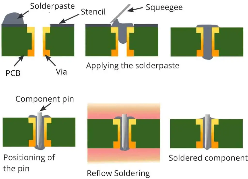
Pin in paste (PiP) is an advanced soldering technique used in printed circuit board (PCB) assembly. PiPprinting deposits solder paste inside through-hole vias and pads prior to component placement. This enables soldering the through-hole pins and PCB in a single reflow pass. PiP provides benefits over traditional wave soldering or selective soldering methods for through-hole components. This article will provide an in-depth overview of PiP technology, processes, advantages, and implementation considerations.
Overview of Pin in Paste Basics
Pin in paste soldering involves:
Depositing solder paste into through-hole PCB locations
Mounting components on the solder paste deposits
Reflowing to solder component pins and PCB in one step
This contrasts with:
First inserting pins through empty holes
Then wave or selective soldering the pins
PiP enables efficient all-surface-mount assembly without separate soldering passes.
Optimizing PiP print quality and reliability involves attention to:
Paste Deposit Accuracy
Paste must cleanly dispense inside holes without smearing or shifting during placement.
Minimum Paste Volume
Only sufficient solder paste to form the joint should be dispensed to avoid overflow.
Component Pitch Range
Printing can accommodate fine pitch but not ultra-fine component spacing.
Hole Wall Preparation
Oxides inside drill walls may require plasma treatment to enhance wetting.
Solder Mask Expansion
Solder mask overlaps onto pad copper improves capillary flow.
Reflow Profile
Dual speed profiles with extended soak above liquidus often works best.
Careful process engineering is needed to implement PiP effectively.
PiP Design Rules
To enable reliable PiP soldering, PCB designs should follow guidelines:
Via Pad Diameters – 0.3mm to 1.0mm range preferred
Annular Rings – 0.25mm to 0.5mm annular rings around drilled holes
Hole Spacing – No closer than 3x hole diameter side-to-side
Copper Plating – ≥25μm copper thickness in holes
Solder Mask Expansion – 0.05mm to 0.15mm onto pad copper
Pad Shapes – Round holes easier than slotted holes
Adhering to these PiP design rules ensures paste can dispense and solder can wick effectively.
PiP Applications
Components suitable for pin in paste soldering include:
Through-hole connectors
Press-fit pins
Transformers, inductors, and coils
Switches and relays
Terminal blocks and screw terminals
Regulators and heat sinks
LED displays and indicators
PiP enables mixed SMT/through-hole assemblies combining advanced and legacy components.
Pros and Cons of PiP Technology
Pin in paste offers advantages but isn’t ideal for all situations:
Advantages
Lower capital equipment costs
Improved joint quality and reliability
Design flexibility
Lead-free processing
High density assembly
Disadvantages
Tight process controls required
Potential tombstoning without adhesive
Additional paste deposit step
Fine pitch components challenging
Hole wall preparation may be needed
Assemblers should weigh the tradeoffs versus production volumes, cost targets, and product complexity when considering adopting PiP.
The Future of Pin in Paste Soldering
PiP utilization continues growing as dispensing accuracy improves and designs shift towards mixed SMT/through-hole assemblies. Continued progress in solder paste formulation, hole wall surface finishes, and advanced profiling will further expand PiP soldering adoption. Its flexibility and technical capabilities position PiP well for meeting future electronics assembly requirements.
Conclusion
Pin in paste soldering delivers an efficient process for assembling through-hole components without wave or selective soldering equipment. By dispensing solder paste into PCB pads and vias prior to placement, reflow can solder pins and through-holes in one pass. With tight process controls and design considerations, PiP enables high performance mixed technology assemblies. As demand grows for flexible, high-mix production, PiP stands poised to become an increasingly valued assembly process option.
Frequently Asked Questions
Q: What types of solder paste are used for pin in paste processes?
Standard “no-clean” SAC305 solder pastes are suitable for many PiP applications. For challenging situations, solder pastes engineered specifically for PiP with wider reflow profiles may be preferred.
Q: Does PiP allow double-sided reflow soldering?
Yes, PiP printing can be done on both sides of a PCB followed by double-sided component placement. Dual reflow would then solder all joints in one pass. This further simplifies processing.
Q: How does PiP soldering compare cost-wise to wave soldering?
Eliminating wave soldering equipment provides significant cost savings on lower to medium volume production. For very high volumes, dedicated wave solder may still be more cost effective than PiP bypassing capital expenses.
Q: What are the limitations on component pin pitch with PiP?
The finest pitch achievable with PiP is around 1mm pin spacing depending on hole size. Ultra-fine pitch components may still require traditional soldering approaches.
Q: Can solder paste be dispensed into plated through holes or is plating needed?
PiP printing can work with both plated and non-plated holes. But plating provides stronger metallurgy for soldering. Preparation may be needed on non-plated holes walls.
Pin in Paste (PiP) Technology in SMT Assembly:
We all know the increasing technological advancement in electronics industry, the core reason for which is the growing competition among PCB manufacturers and suppliers. Every PCB CEM (Contract Electronic Manufacturer) is find new ways to cut cost, increase quality and shorten the lead time of PCBs fabrication, assembly, testing and delivery. So talking about the cutting the cost is a highly significant in increasing profit gains and thus ultimately leading the particular CEM in the race of PCB manufacturing competitors.
There are many ways to reduce the manufacturing cost of PCB fabrication and assembly like PCBs with multiple layers are mostly High Density Interconnect (HDI) PCBs, so they are expensive as compared to single or double layer PCBs, so in order to compare the cost analysis of PCB manufacturing, it is important to consider two PCBs with same parameters like they both should be multilayer, HDI and SMT + THT components based. However the difference making aspect in terms of cost analysis are the 1- Surface Finish methods 2- PCB components selection 3- Component Sourcing 4- Process cost 5- Labor Cost and 6- Overhead expenses can determine the ultimate cost per PCB that is produced by CEM.
In this article we will discuss the most powerful method of component mounting in prototype PCB assembly process that will ultimately reduce the cost of manufacturing and speed up the process thus resulting in less lead time.
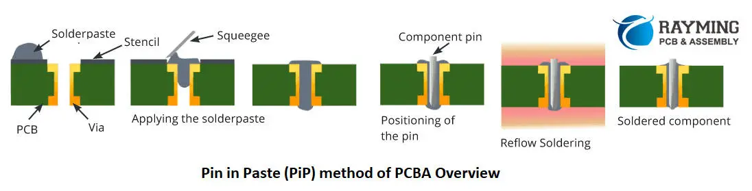
Comparison of Commonly Practiced SMT/THT PCBA and PiP:
While the most of the PCB manufactures and assemblers use the reflow soldering method for SMT (Surface Mount Technology) components assembly and then manual soldering or wave soldering of THT (Through Hole Technology) components, the best method to carry out is the PiP (Pin in Paste) method. The following flow chart shows the common process flow of SMT and THT components assembly.
Now in contrast to the above process flow, the PiP (Pin in Paste) PCBA process flow is lot simpler and easier. Checkout the below mentioned PiP process flow chart.
As you can see that the process is shortened tremendously, this is because the SMT and Through-hole components are baked by the same Reflow Oven that was used to bake only SMT parts. The PiP process is simplified in following manner.
1- The additional process of manual assembly of THT electronic components is eliminated
2- Wave Soldering is not required
3- Additional PCB Assembly process setup machine i.e. Wave soldering machine is not required
4- Additional labor not required to work on PCB coming out of vacuum reflow oven
1- Elimination of capital equipment like wave soldering machine, laser soldering machines or any other equipment associated with Through hole soldering
3- Cost can be saved by reclaiming floor space used in the wave and hand soldering processes.
4- Material cost saving like solder bars, fluxes, wave solder pallets and other hazardous materials in the wave solder process.
5- Other indirect incentives lesser number of through-hole connection by replacing THT components to their equivalent SMT and reduction in heating operations. Because various stages of heating cycle like reflow, wave or hand soldering can increase the risk of damage to the board and component, hence eliminating the wave and hand soldering methods in PiP is a big benefit.
6- The greatest advantage of PiP is the ability to design PCB with complex components on bottom side, in traditional process most complex components can only be placed on top side of PCB because they are not able to pass through the wave solder process. By eliminating the wave solder process the PCBs can be designed with complex components on both top and bottom side. This makes it easy to design smaller and denser PCBs for smaller electronic devices
So what is actually PiP technology..?
As we know that the Through-Hole components are those that have pins/leads and they need to be inserted into the PCB holes and then soldered manually or by wave soldering machine. A technology that was first used in 1985 by Motorola to solder the THT components in reflow soldering oven and that made strong joints though.
In the pin-and-paste technology, also known as THR (= Through-Hole-Reflow) technology leaded components (THT) are soldered in the reflow process. Paste is printed by means of stencils or dispenser into the through holes for the pins and the through-hole components are assembled on the board. The Pin in Paste PiP is also known as intrusive reflow, Reflow on through hole (ROT), Solder paste on Through Hole technology (SPOTT) and Alternative assembly and reflow technology (AART).
How is PiP Done.?
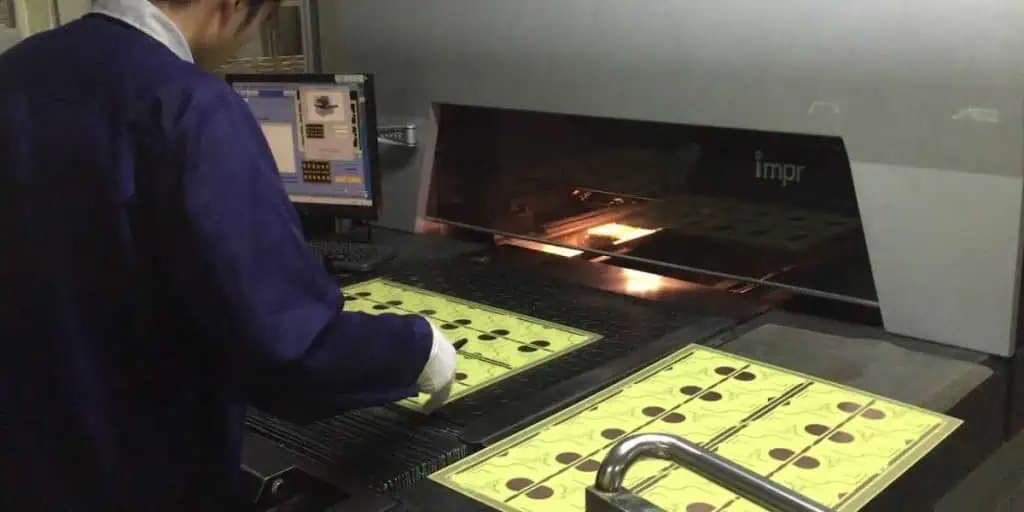
First of all, the circuit board is printed with solder paste in stencil printer. The stencil printer apply the solder paste on all SMT and THT components locations. Then it may pass through the dispenser for manual dispensing of solder paste, then the SMT and THT components are placed on PCB by means of pick and place robot. After this the whole assembly is placed in vacuum reflow soldering oven, where the solder paste is melted and SMT plus THT components are soldered on PCB. This seems a lot simpler process flow but it can have several challenges which are mentioned below.
Usually the manual hand driven solder paste dispenser is suitable for prototype PCB assembly process where larger production run of PCB is not the case. An example of solder paste dispenser syringe is shown in figure. In the prototyping case, the manual components handling/placement on PCB is recommended.
1- The through hole THT and SMT surface mount components are needed to be baked in Reflow oven hence they (whole component including terminal and plastic body i.e. casing) must have capability to withstand high temperature like 260OC for 10 seconds.
2- Because some THT components do not have their equivalent SMT versions so those THT components have to be assembled on PCB and cannot be avoided.
3- The THT component should be selected such that its housing/casing construction allow a visual inspection of the solder joint.
4- A protective stand-off pad beneath the component’s casing/body must be placed to ensure there is no touching/contact with the solder paste during reflow process.
5- The high speed automated pick and place robot can grab the THT and SMT component from its planar surface to place it on PCB.
6- It can be difficult to provide an adequate solder paste for through hole joints with stencil printing process.
These challenges can be covered by properly focusing on the requirements of Pin in Paste PCB assembly. Some of them are discussed here.
Component Requirement:
1- The component SMT or THT selected for PiP must survive the high temperature of reflow oven
2- The THT components must be selected in a way that it fits the requirements of SMT pick and place robot machine, to be picked and placed on PCB automatically and accurately. These requirements are the component height, component shape and spacing between component pins.
3- The layer of tin must be coated on top of vias for THR (Through Hole Reflow), hence to achieve this, the minimum distance between component and PCB should be between 0.3mm to 0.7mm and the THT component lead should be 1.5mm thicker than the PCB thickness in order to meet IPC3 standard.
Component Pad Requirements:
1- It is recommended that the smaller components placed on bottom side and larger components on top side. A minimum of 2mm spacing must be kept around PIP components; if there are multiple PIP components then at-least 10mm spacing between adjacent PiP components must be ensured to avoid interference during automatic mounting by Pick and place robot.
2- The distance between adjacent through hole centers should be at least 2mm, distance between edges of adjacent pads should be at least 0.6mm, distance between pad edge and aperture diameter should be at least 0.3mm. Pad aperture diameter should be larger than component pin diameter by 0.2 to 0.4mm. This is done to avoid tin connection between adjacent pins or between pads.
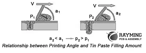
1- The most important parameter for stronger solder joint is the amount/volume of solder paste being printed by stencil, this is governed by diameter of through holes, thickness of substrate and lead shape. The tin paste must fill the electroplated through hole and fillets are on the top and bottom of PCB.
2- The amount of tin paste required by THT solder joints is larger than the required by SMT
3- Usually the flux fills the 50% of the volume of plated through-hole and remaining 50% is filled by tin paste, hence air bubbles or voids can form when the flux is volatized after soldering process. This can be troublesome, so suitable amount of solder/tin paste must be applied on each through-hole pad.
4- The ideal tin paste filling must be greater than 90% and tin paste filling amount in through holes must be greater than bottom pad by 0.5 to 1mm. A squeegee angle of 45Ois reasonable however the smaller the squeegee angle the more then tin paste is filled in the through hole and greater the angle the lesser the tin paste fill in through hole as show in diagram below where V velocity is constant in both cases.
Reflow Oven Requirements:
The reflow oven temperature settings allow the smooth and steady heat transmission through radiation to the solder pads of SMT and solder joints of THT. As can be seen from the typical reflow temperature profile, the liquidus is at 217OC for 45-75 seconds. This is actually the reflow window, however the slow ramp of 1-3OC is important for stable temperature rise and then degrading the temperature uniformly at the rate of 2-4OC finishes of the reflow process.
Conclusion:
Summing it up all, we can say that PiP (Pin in Paste) method of PCB assembly is extraordinarily useful for mass production of smaller, denser and lighter PCBAs which can cut the cost of production tremendously. With Pin in Paste technology one can have a stronger and better THT solder joint as that of manual or wave soldering and can place complex SMT components on both sides of PCB thus optimizing PCB board space and miniaturizing electronic devices.
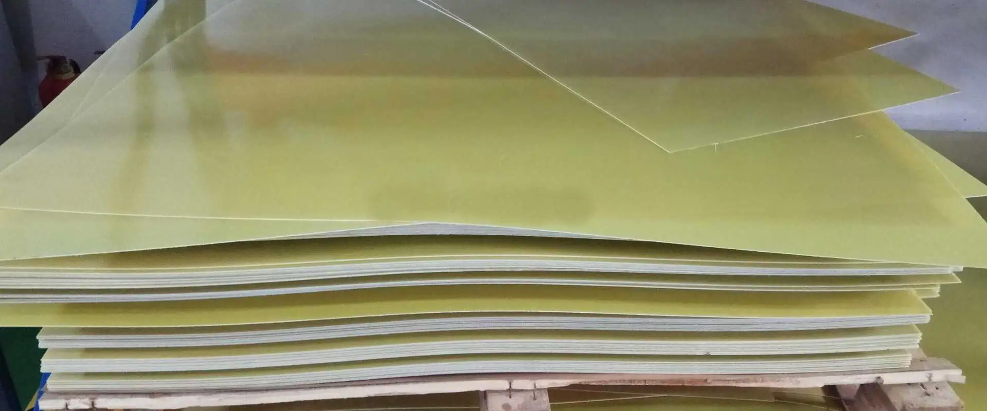
Copper clad laminate (CCL) forms the basic structure of printed circuit boards. CCL consists of a central insulating core material sandwiched between layers of copper foil. The manufacturing process to create quality CCL utilizing epoxy resin involves multiple steps including impregnation, lamination, copper bonding, and final finishing. This article will overview the end-to-end CCL production process using epoxy resin chemistry.
Overview of CCL with Epoxy Resin
CCL material consists of:
Central insulating dielectric core
Layer of copper foil on each side
Epoxy resin throughout core
The core provides mechanical support. Epoxy resin gives chemical adhesion and bond integrity. Copper foil enables circuit patterning.
Epoxy resin CCL offers:
High bond strength
Good thermal performance
Excellent chemical resistance
Long-term reliability
Cost effective manufacturing
Epoxy resins are the most common resin system used in PCB materials.
Producing quality CCL with epoxy resin involves the following key steps:
1. Core Material Preparation
The insulating core material comes in sheets consisting of woven fiberglass cloth. The material is inspected, cleaned, batched, and staged for impregnation.
2. Resin Mixing
Liquid epoxy resin is weighed and mixed with hardeners and other reactive additives to form the impregnation resin. The mix is filtered for cleanliness.
3. Impregnation
The core material is pulled through a tank of prepared resin. The woven glass cloth fully wets out as resin penetrates evenly throughout each sheet. This stage determines final resin content.
4. B-Stage Oven Curing
The impregnated core material is pulled through a long heated tunnel oven. Heat causes partial curing of the resin into a tacky B-stage state ready for lamination.
5. Copper Foil Bonding
Rolls of thin copper foil are pressed onto both sides of the impregnated, B-stage core material. The assembly then enters a heated nip roller press.
6. Autoclave Lamination
The copper clad sheet enters an autoclave chamber. High pressure and heat fully cures the resin bonding the foil to the core into a solid laminate.
7. Cooling
After autoclave curing, the laminate passes through a cooling zone to bring CCL temperature back down for additional processing.
8. Roller Treatment
Roller presses apply mechanical pressure to ensure lamination uniformity, remove any air pockets, and improve surface smoothness.
9. Machining
Computer numeric control (CNC) routers machine the CCL into standardized sheet sizes with beveled edges. Holes may also be drilled.
10. Quality Inspection
100% inspection of CCL sheets checks for defects, thickness, hole quality, and other metrics to ensure specifications are met.
11. Packaging
Inspected sheets are carefully packaged to avoid damage prior to shipment or further PCB processing.
The CCL sheets must meet exacting standards to endure PCB fabrication, assembly, and service life. Strict process controls provide consistent, high-quality CCL product.
Key Process Considerations
Several factors are critical during CCL manufacture:
Resin Content
The amount of resin solids impregnated into the woven glass must stay within a target range. Too much or too little resin impacts properties.
No Voids
Air pockets between glass fibers or delaminations create weak points that can cause PCB failures.
Controlled Thickness
Consistent core thickness is critical across each CCL lot. Thickness uniformity impacts subsequent PCB processes.
Bond Integrity
Strong, uniform bonds between resin, foil, and glass withstand PCB processing stresses and temperature cycling.
Dimensional Stability
Sheets must exhibit minimal curling or shrinking to avoid registration issues during PCB imaging and etching.
Cleanliness
No residue or foreign material can remain on surfaces or in the core to prevent PCB defects.
Maintaining strict tolerances and disciplines for these parameters ensures reliable CCL quality.
Dimensional Stability Analysis – Quantifies shrinkage and expansion
Electrical Testing – Verifies dielectric breakdown voltage
Statistical process control with extensive testing provides the assurance of product quality and consistency.
Conclusion
Manufacturing reliable copper clad laminate utilizing epoxy resin requires careful process control and validation. When executed properly, CCL provides the robust foundation needed for further PCB fabrication and assembly into quality electronic products. The combination of high performance resins, sturdy core materials, and advanced manufacturing techniques enables CCL to serve its vital role in the production of printed circuit boards.
Frequently Asked Questions
Q: Why is fiberglass most commonly used as the core material in CCL?
Fiberglass provides an optimal balance of mechanical strength, dimensional stability across temperature variations, dielectric performance, and cost-effectiveness. The woven glass cloth construction also absorbs resin effectively during impregnation.
Q: What are some key advantages of epoxy resin systems?
Epoxy resins offer high adhesive strength, chemical and moisture resistance, good dielectric properties, processing versatility, and cost efficiency. These characteristics make epoxies ideal for electrical applications.
Q: What is the difference between FR-4 and other common CCL designations?
FR-4 is a specific flame-retardant grade of CCL made from brominated epoxy resin and E-glass core. Other grades like G-10 and FR-5 indicate different resin systems, core materials, and characteristics optimized for specific applications.
Q: How does CCL thickness tolerance impact PCB manufacturing?
Consistent CCL thickness is critical for maintaining registration during layer-to-layer imaging and etching processes in PCB fabrication. Tighter thickness tolerances enable higher density PCB technologies.
Q: What is the purpose of beveled edges on CCL sheets?
Beveled edges prevent sharp corners from damaging handling equipment or operators. The angled edges also help avoid peeling or lifting during inner layer lamination in multilayer PCB fabrication.
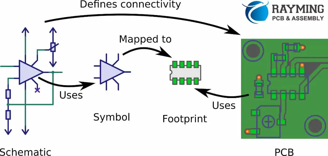
In printed circuit board (PCB) design, the terms “footprint” and “land pattern” are sometimes used interchangeably. However, there are distinct differences between the two. Understanding these subtle differences can help optimize PCB development workflows and avoid mishaps during manufacturing. This article will examine footprints and land patterns in detail, how they complement each other, and best practices for implementation.
Footprints for PCB Assembly
A footprint represents the physical footprint that a component will occupy on the assembled PCB. The footprint provides an outline of the component body and visually indicates how much board space that component consumes.
Key elements of a footprint include:
RefDes – Component reference designator like R1, C112, U3, etc.
Body outline – Rectangular or other shape showing component boundaries
Pin location holes – Placement of pins for through-hole components
Assembly information – Reference text, polarity markings, identifiers
Courtyard – Area that must be kept clear around component
The footprint does not define actual copper pad shapes for connecting to the component. It only provides an abstraction of the component location and space requirements needed for PCB assembly planning.
The land pattern defines the physical pads, traces, and copper features needed to electrically connect to pins or leads on the component. Land patterns specify where copper will exist on fabrication layers.
Typical land pattern elements:
Contact pads – Surface mount pads, through-hole annular rings
Traces – Interconnecting copper between pads
Thermal relief – Spokes and shapes to reduce thermal pad solder wicking
Land patterns constitute the physical design data for manufacturing, determining how the PCB will actually be fabricated.
Relationship Between Footprints and Land Patterns
The footprint and land pattern both relate to the same component but serve different purposes. The footprint provides assembly information while the land pattern gives manufacturing specifications.
During PCB design, footprints are assigned to components in schematic symbols. These footprints are then placed on the layout canvas to allocate space and plan routing.
The linked land patterns define the actual pads and traces that will connect to the component. The shapes from multiple land patterns together determine the fabricated board geometry.
Well designed footprints and associated land patterns are required for a successful PCB development process.
Here are some best practices for working with footprints and land patterns:
Footprints
Create distinct visually recognizable footprints for each component
Include reference designators aligned consistently
Provide polarity markings and text per datasheet examples
Follow IPC guidelines for courtyard spacing from body
Define layer on top for optimal visibility
Land Patterns
IPC-7351B provides industry standard pad dimensions
Follow datasheet recommendations for unique pad designs
Include thermal relief shapes if a thermal pad
Add fiducials or other fabrication features as needed
Assign appropriate copper and mask layers
Linkage
Use naming conventions to associate related footprint & land pattern
Verify footprints link to intended land pattern files
Check land pattern when inspecting footprint placement
Keep footprint visuals consistent with land pattern geometry
Following these guidelines helps optimize the PCB design process while avoiding misalignment issues during manufacturing.
Footprint and Land Pattern Creation
In ECAD tools like Altium, OrCAD, and Pads, footprints and their associated land patterns are designed in the library editor module. They are then saved into the tool’s database libraries to be reused across designs.
The component land patterns from the integrated library get merged together to form the overall PCB fabrication data. Keeping footprint visual appearance synchronized with the land patterns ensures accuracy.
Some best practices for library footprint/land pattern creation include:
Design footprint and land pattern together as a single component object
Validate footprints are dimensionally aligned with their linked land pattern
Use consistent naming conventions between associated footprints and land patterns
Verify pad stack and electrical connectivity in the land pattern
Simulate footprint placement on land pattern to check alignment
Cross-probe between footprint and land pattern views
Following a consistent, integrated process for footprint-land pattern development avoids issues down the line.
Land patterns deliver manufacturing specifications
Footprints and land patterns must align
Follow IPC guidelines for industry standards
Use consistent modeling and naming conventions
Validate linkage between footprint and land pattern
Keeping these best practices in mind will optimize efficiencies and accuracy in PCB design workflows and library management as footprints and land patterns fulfill their complementary roles.
Frequently Asked Questions
Q: Can you update just the footprint or just the land pattern independently?
It is possible to edit either the footprint or land pattern independently. However, any changes must maintain alignment between the two or manufacturing issues could result. Generally it is best to revise footprints and associated land patterns together to avoid inconsistencies.
Q: Should land patterns include text labels and reference designators?
Land patterns should not contain text labels or refdes text. Land patterns define only copper features. Including text would interfere with copper fill regions during fabrication. Reference designators belong solely on the assembly footprint.
Q: Can custom pad shapes be created in land patterns?
Yes, land patterns can include custom pad shapes beyond basic circles or rounded rectangles. Unique shapes are often required for large exposed die pads. However, too much complexity adds manufacturing cost. Standard shapes still work best for common pad requirements.
Q: How are 3D body models related to footprints and land patterns?
3D body models provide visual depth and component height information missing from the basic 2D footprint. However, 3D models visuals must still align accurately with both 2D footprint outlines and related land pattern copper.
Q: Can footprints and land patterns be synchronized after creation?
If footprint visuals and land pattern pad geometries become unsynchronized, tools like Altium provide compile design features to realign them. For optimal library management, it’s best to maintain synchronization during initial development.
The design of printed circuit board is not only related to creation of schematics and its Pcb layout but there are numerous other terminologies which must be understood. Such as the symbols are abstracting functions of different components and are communicating as the interface among both schematic reader and software. Therefore, to this point, there is a need of definition of the connecting points for entire schematics with points referred as pins. Certain artwork is also introduced in to the symbols for its effective utilization. The simplest symbol of all is known as the black box symbol and it is merely surrounding the symbol through box in which each pin is having a meaningful name. For a few of the symbol classes, there are certain standards defining the outlook of such symbols. Some of the standards of the symbols are incompatible to each other, therefore you have to be inspired of the standard which is best suiting your purpose.
The PCB footprint is defined as the physical interface among electronic components or land pattern and printed circuit boards which is also comprising of the information of documentation such as reference, polarization mark, and outline. The land patterns are either derived from the dimensions of the component’s tolerances included or taken from the datasheet. This all is as per the standards of industry. Most probably the land patterns are also derived from same standard. It must have all of the connection points which are known as pads for soldering all of the electronic components over sit. The size, position, and shape of the pads must be aligned with the specifications of the datasheet for avoiding faults.
The pads are defining the features to be appearing on the paste layer, masks, and copper. The copper is known as the area which is covered by copper layer. Masks are the cutout region over the layer of solder mask, whereas paste the region of cutout over solder paste stencil which is utilized for the reflow soldering. The courtyard area is where none of the components are to be placed. The courtyard area is usually very large than that of combined parts body and pads area.
It is considered as beneficial when having an outline for the pins and component body over the silk screen for de-bugging and soldering. However, it must be made sure that all of this must be visible after the process of assembly i.e. the outline of silk must be larger than that of the body of components. The layers of fab over the artwork is very beneficial in case if you need the documentation on the board. However, in such a case, it must be having the entire outline of the body including the pin markers.
Both terms footprint and land patters are usually utilized interchangeably in the printed circuit board assembly process in the industry. While, both terms are quite similar to each other, however, still there lies a nuance which is drawing a differentiation among both terms. Sometimes, it is said that the differentiation among both terms is somehow pedantic, however the truth lies that more often the functionality of both terms is different after understanding it. It is a fact that certain component might have dissimilar land pattern however it is going to have a single footprint always.
The footprint of a component is officially referring to the actual physical size of that specific component. Therefore, if you are to measure the leads and body thoroughly of certain given component and drawing a picture through utilization of the dimensions, then you may have the part of the footprint. To picturize the concept in a more relevant way, the footprint of any component is much similar to the footprint of a human or person as it is imprinting the component’s print if pressed down through hands.
The land pattern is referring to the size of the pads and its outline for a given component or part of the printed circuit board that must be designed. Both of the automated and manual processes of soldering is requiring that the designed pads for all of the parts of the printed circuit board must be larger than its leads where these components are supposed to be soldered. This is to make it possible for the land patterns to be slightly larger than that of the footprint of every component. The datasheets of manufacturers are mostly having the required information of the land patterns.
Services of RayPCB
Among the highly appreciated aspects of the RayPCB, one of the aspects is its service of thorough DFM check of comparison of land pattern vs.PCB footprint. Before the process of pcb fabrication to begin, the expert engineers of RayPCB are checking the quality management and is comparing the land patterns of each and every part of the design which that of the dimensions of documented footprint for making it sure to have a higher quality assembly process of printed circuit boards. This service of RayPCB is anticipating many of the common defects that incur while manufacturing process of printed circuit boards because of dissimilarities among the pcb footprints and land patterns.
Therefore, if you have queries regarding PCB footprints and land pattern associated to the design, fabrication, and assembly process of your printed circuit board, please feel free to contact our customer service agents who are available to serve you 24/7 a day. You can visit our website online and then go to contact us form, filling your query related information and our customer representative will soon contact you with the best possible solution. You can either call on our toll-free number mentioned on our website to contact a customer representative immediately and seek help regarding your confusions. Moreover, you can also email us your queries giving details of the problem or question that you are facing. We will give a detailed response of your email giving you satisfactory answers to your questions. We are always looking forward sharing a friendly bond with our customers which bring them back to us in future for more projects.
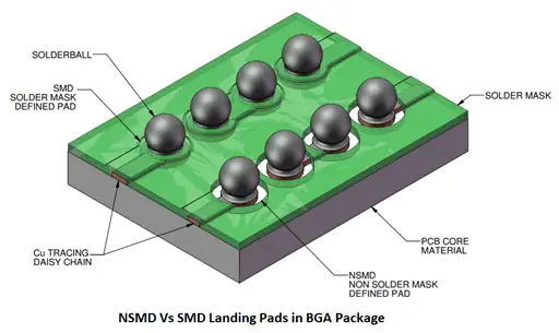
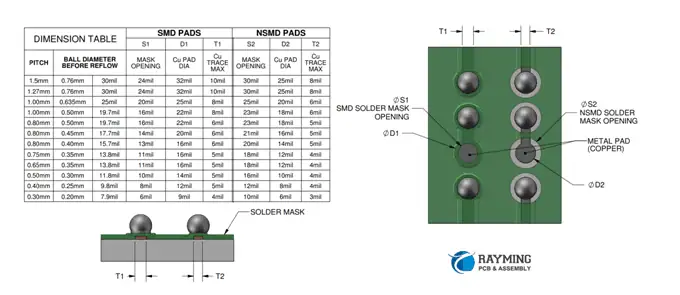
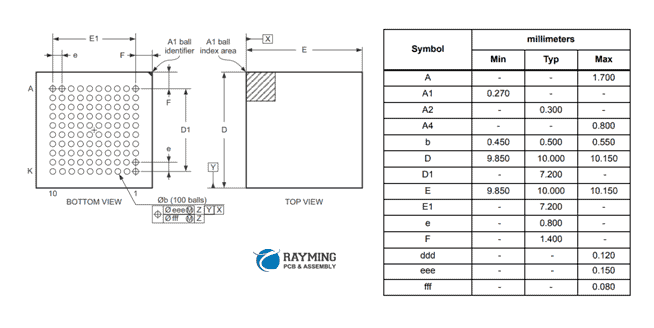
Ball grid array (BGA) packages have become a mainstay of modern electronics, offering high density interconnection in a small footprint. But properly laying out a printed circuit board for a BGA device does require special considerations versus other package styles. This article will provide guidance on key factors when designing BGAs including pad dimensions, placement, routing, thermal design, and board-level reliability. Following these PCB design recommendations will help ensure successful implementation of BGA packages.
Overview of BGA Packages
First, a quick overview of BGA technology:
Package surface mounts to PCB via an array of solder balls
Ball pitch ranges from 0.5mm to over 1.5mm
High density interconnection – Over 1,000 pads/balls
Thoroughly vetting the design avoids integration or production issues down the line.
Conclusion
Designing a PCB for a ball grid array device involves special considerations for routing, thermal management, manufacturability, and reliability. Following IPC guidelines and package-specific recommendations helps ensure your BGA implementation meets performance and quality standards. While requiring more planning, close collaboration between designer and manufacturer enables successfully deploying BGAs and gaining the benefits of the high-density interconnect technology in your products.
Frequently Asked Questions
Q: How fine of a pitch is achievable with newer BGA packages?
A: Packaging advances are enabling finer BGA pitches below 1mm, including 0.8mm and 0.65mm. This provides interconnect densities over 2500 pads/balls. However, PCB fabrication and assembly requires tighter tolerances at finer pitches which can increase cost.
Q: What are common solder ball materials used with BGA packages?
A: Solder ball alloys are typically eutectic SnAgCu (SAC). High lead solder is still used for some applications requiring high reliability. Lead-free solders are becoming standard due to regulatory pressures to eliminate lead.
Q: What are indications of potential BGA solder joint defects?
A: Excessive voids in solder joints, pad cratering, non-uniform or missing solder fillets, solder bridging, thermal pad dry joints, and cracked joints are defects that can lead to failures. X-ray inspection after assembly is recommended to identify issues.
Q: How many PCB layers are typically required for complex BGA designs?
A: High density BGA designs often require at least 6 to 8 layers. Critical signals need routing on inner layers with reference planes above and below. More layers provides additional routing channels to relieve congestion under devices.
Q: What are common causes of solder joint failures in BGA packages?
A: Thermal expansion mismatch, mechanical stresses, vibration, solder voids, dry joints, poor pad design, and moisture absorption can all contribute to eventual BGA solder joint failure over temperature cycling in the field. Following reliability design rules helps mitigate risks.
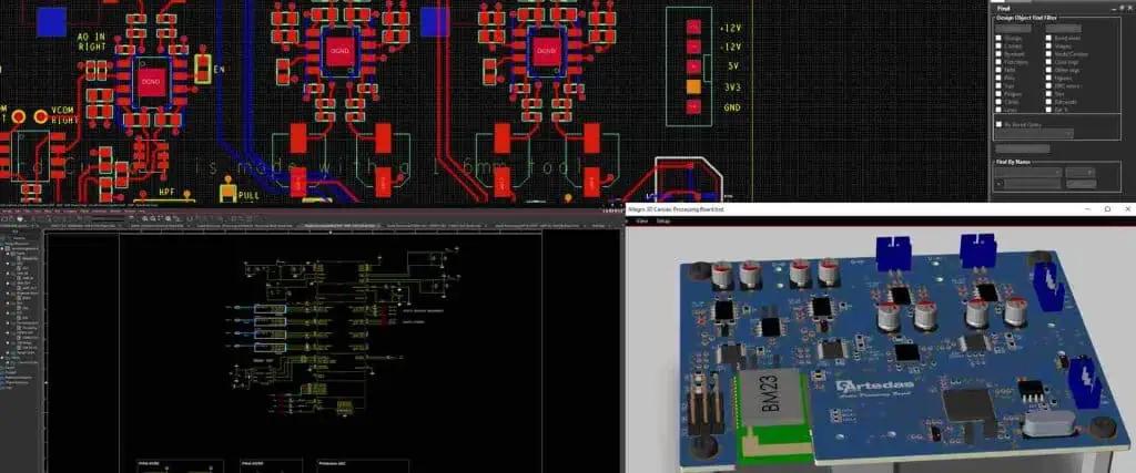
Printed circuit board (PCB) design is a complex process involving schematic capture, board layout, auto-routing, design rule checks, signal and power integrity analysis, thermal analysis, and much more. With products becoming more advanced, PCB designers need electronic design automation (EDA) tools that can handle rising complexity while improving productivity. This article will review ten leading PCB design software platforms available today based on features, capabilities, and ease-of-use.
Overview of PCB Design Flow
Before diving into the tools, let’s briefly summarize the typical PCB design flow supported by EDA tools:
Schematic capture – Draw the electronic schematic showing components and their electrical connections.
Symbol creation – Make symbols to represent components on the schematic.
Altium Designer is widely considered the most advanced and complete PCB design system available. It’s loaded with features spanning the entire design process from schematic capture to manufacturing outputs.
With unique innovations like ActiveRoute automated routing, Altium provides sophisticated capabilities that enhance designer productivity and workflow.
2. Cadence Allegro
Cadence Allegro offers a complete scalable PCB design environment targeted at high performance electronic applications. It contains advanced capabilities tailored for high speed design.
Key Features:
Robust design planning and process management
Constraint-driven design flow
Proprietary physical routing engine
Timing-driven layout tools
Extensive visualization capabilities
Flexible schematic editing tools
Interoperability with multiple analysis tools
library creation and management
Manufacturing output automation
Allegro provides high speed design capabilities critical for technologies like PCIe, Serdes, and DDR.
3. Mentor Graphics Xpedition
Mentor Graphics Xpedition enables enterprise-level PCB design addressing advanced users to casual occasional users. It is customizable and integrates with DFM tools for manufacturability.
Key Features:
High speed design features
Unified design environment
Manufacturing preparation automation
Custom reporting capabilities
Integrated library management
Scripting and automation
Multi-user collaboration
Interfaces to MCAD tools
DFx design guidance
Integrated PLM support
Xpedition balances high performance design capabilities with accessibility for a range of users.
4. OrCAD PCB Designer
orcad PCB
OrCAD PCB Designer provides a full PCB design workflow with specialized options for high speed, high density, and flex/rigid-flex boards. It offers advanced productivity features.
Key Features:
Constraint-driven, synchronized design flow
Interactive routing engine
Customizable DFM analysis
Real-time design feedback
Extensive component library ecosystem
High speed, signal, and power integrity analysis
Team collaboration capabilities
Custom reporting and scripting
Manufacturing output automation
OrCAD balances features and usability for cost-effective, capable PCB design. It integrates well across the entire electronics workflow.
Zuken CR-8000 is a proven PCB design solution for surface mount and complex multilayer boards. It features multi-board assembly and 3D packaging capabilities.
Key Features:
High speed design capabilities
Constraint manager for controlled flows
Multi-board assembly design
Photorealistic 3D visualization
Flexible layout editing tools
DFM analysis and verification
Library creation and custom reporting
Manufacturing documentation automation
Interfaces with MCAD tools
CR-8000 balances functionality with ease of adoption for seamless PCB design. The 3D packaging design environment helps streamline the electronics workflow.
6. Pulsonix PCB Design
Pulsonix PCB Design is an intuitive, easy to adopt platform with excellent usability. It offers advanced functionality like design reuse, manufacturing automation, and interactive routing suitable for many applications.
Pulsonix offers superb usability without sacrificing capable performance for mainstream PCB applications.
7. Autodesk EAGLE
Autodesk EAGLE is known for affordability combined with powerful features. Different pricing tiers allow customization for hobbyists, startups, and advanced users.
Key Features:
Easy to learn user interface
Extensive component libraries
Real-time DRC during routing
XML data exchange capabilities
Custom scripting and user language programs (ULPs)
Mixed-signal schematic and layout
Multi-sheet schematics
Integrated version control
Third party integrations via APIs
EAGLE continues gaining mainstream share given its balance of ease-of-use and capability at reasonable cost.
Pads Professional enables concept through production PCB design with powerful automation and reuse capabilities.
Key Features:
Rules and constraint-driven flow
Interactive routing engine
Sketch routing capabilities
Intelligent component placement
Integrated MCAD collaboration
Automated manufacturing documentation
Role-based design collaboration
Programmable automation interface
Packaged part reuse and automation
Library lifecycle management
PADS leverages automation and customization for efficient PCB design tailored to specific user needs and applications.
9. Solidworks PCB
Solidworks PCB provides a single integrated environment to support the entire electronic development process including MCAD collaboration.
Key Features:
Multi-board assembly design
Constraint-driven, synchronized workflow
Real-time DRC during layout
Integrated ECAD/MCAD component reuse
Automated manufacturing documentation
Design reuse and automation
Revision control and design history
Custom library development
Programmatic automation interface
Team collaboration capabilities
Solidworks PCB tightly couples the electronic and mechanical design workflows for streamlined product development.
10. Altium Concord Pro
Altium Concord Pro provides cloud-based PCB design capabilities accessible from any browser. It’s ideal for global team collaboration.
Key Features:
Cloud-based design environment
Managed component libraries
Interactive routing engine
Real-time design rule checking
Unlimited file storage and history
Automated outputs and documentation
Seamless team collaboration
Task management and notifications
Custom reporting and visualizations
Role-based access control
Dashboards and analytics
For organizations seeking a cloud-based PCB design platform, Altium Concord Pro is purpose-built for the task.
Conclusion
This lineup of leading PCB EDA tools demonstrates the breadth of options available today. From advanced capabilities like high speed signal analysis to cloud-based global team design, these platforms enable productivity and innovation across the PCB workflow. For organizations evaluating PCB design systems, this overview provides a starting point to narrow down your shortlist based on feature needs, budget, and electronic design culture and ecosystem. By matching organizational requirements to tool strengths and deployment models, engineering teams can leverage PCB design automation to achieve product goals and accelerate market success.
Frequently Asked Questions
Q: What are the main advantages of an integrated PCB design tool?
A: Integrated tools with unified schematic, layout, library management, and manufacturing capabilities reduce tool switching and streamline workflow. Integrated tools also enable greater synchronization between domains and automation across the design flow.
Q: How important are library and component management capabilities in a PCB design system?
A: Library capabilities are very important. Ready access to comprehensive component libraries speeds design time by eliminating repetitive symbol and footprint creation work. Library lifecycle management also assures designers access the right validated library elements rather than outdated or unapproved footprints.
Q: What training is required to become proficient in a PCB design tool?
A: Most tools can be learned in 40-80 hours of hands-on training. Learning the basic features can happen faster. But mastering advanced productivity tools and workflows takes longer. Formal training is recommended to gain proficiency faster. Some tool providers offer certification programs to document tool expertise.
Q: What are DRCs and why are they important in PCB design?
A: Design rule checks validate a PCB layout adheres to specified clearances, spacing, trace widths, and other constraints. DRCs are critical for ensuring manufacturability, reliability, and performance. DRCs integrated into the tool avoid surprises late in the design process.
Q: How does Revision Control help with PCB design?
A: Revision control systems record incremental changes and provide version history. This supports parallel workflows and tracks design progress. Revisions enable designers to experiment without risk of losing working baselines. Integrated revision control improves design team collaboration.
Determining the right printed circuit board (PCB) thickness is an important aspect of the design process. The thickness impacts manufacturing feasibility, component clearances, stiffness, thermal performance, weight, and cost. With PCBs becoming more complex including embedding actives and passives, the number of layers increasing, and higher density designs with HDI, selecting appropriate board thicknesses is more nuanced than ever. This article will provide guidance on how to optimally design PCB thickness to meet mechanical, electrical, and fabrication requirements.
Key Factors In PCB Thickness Selection
Several interrelated considerations influence the choice of PCB thickness:
Number of layers – More layers require greater thickness to accommodate inner layer spacing. High layer counts (>36) drive thicker designs.
Component height – Clearance must be allowed between tallest components and outer layers for assembly and preventing shorts.
Routing density – Compact routing of fine features needs thicker cores for trace impedances and layer separation.
Stiffness – Thicker boards provide more rigidity, important for large PCBs and minimizing flex stress.
Flex portion minimum bend radius: 10X board thickness If 0.1” bend radius needed → 0.1/10 = 0.01” minimum thickness
Total Minimum Thickness
Copper: 3.45 mils Dielectric: 15 mils Clearance: 150 mils Bend (N/A here): 1 mil
Total: 168.45 mils (0.168”)
Round up: 0.170” minimum thickness
This methodology can be followed to calculate minimum workable thickness for any PCB stackup and design constraints.
Adjusting Thickness for Functionality
Beyond the bare minimums, PCB thickness is often increased to optimize performance or fabrication. Common reasons include:
Trace Impedance Control – Matching trace impedances requires specific dielectric spacing. Thicker material may be needed between layers to achieve target impedance.
Signal Integrity – Thicker dielectrics reduce capacitive coupling and crosstalk between layers.
Noise Isolation – Additional dielectric layers helps isolate sensitive analog signals from noisy digital routing.
Rigidity – For large boards (>15” edge), increasing thickness adds stiffness to counter flexing forces.
Warpage Reduction – Symmetric center-core construction with thicker dielectrics minimizes warpage from manufacturing stresses.
ESD Resistance – More dielectric buildup helps withstand electrostatic discharges in high voltage applications.
Thermal Management – Added inner layers enables lateral heat spreading while minimizing impact on thickness.
Embedded Components – Cavities for embedded actives and passives require extra thickness.
In each case, the cross-functional design team weighs the tradeoffs of increased thickness against other constraints to find the sweet spot.
Standard Thickness Increments
Rather than arbitrary values, there are common PCB thicknesses used across the industry:
PCB Thickness
Number of Layers
0.031”
2
0.062”
4
0.093”
6
0.125”
8
0.156”
10
0.187”
12
0.218”
14
0.250”
16
These standard thicknesses align with typical layer counts and offer sufficient margins for most applications. They provide a good starting point when estimating initial thickness. As the design progresses, the thickness can be dialed in based on specific requirements.
Of course, specialized or high complexity designs may warrant going outside these general ranges. But they provide a reasonable starting point when estimating thickness by application.
PCB Stackup Configurations
There are several stackup arrangements that impact overall thickness:
Symmetric
Layers are distributed equally about the center core. This avoids mechanical stresses from asymmetric construction. Often used for >8 layer designs.
Asymmetric
Layers are grouped toward one side of the center core. Can cause bowing but uses less dielectric. Often used for simpler <8 layer boards.
Core Thickness
Alternative core thicknesses like 0.024”, 0.049”, or 0.081” can be specified when total thickness requirements differ from standard sizes.
Buried Cores
A buried core adds rigidity for ultra-thin boards. A thin core is laminated between outer buildup layers. Allows high layer count in minimal thickness.
Mixed Cores
Different core thicknesses can be combined for complex requirements. Thinner base cores reduce weight while thicker inserted cores add rigidity.
Copper Balancing
Equal thickness copper layers on extremes minimizes curl and wrinkling. Heavier internal planes provide planarity.
The right stacking arrangement contributes to optimizing the finished board thickness.
Panel Thickness vs Final Thickness
Thickness Ranges
It helps to distinguish between:
Panel thickness – The initial PCB panel thickness through fabrication, often slightly thicker than final thickness.
Final thickness – The completed board thickness after processing. May involve post-fabrication steps like surface grinding to achieve final thickness target.
For example, a 0.100” final thickness board may use a 0.104” or thicker panel to allow for processing variances and finishing.
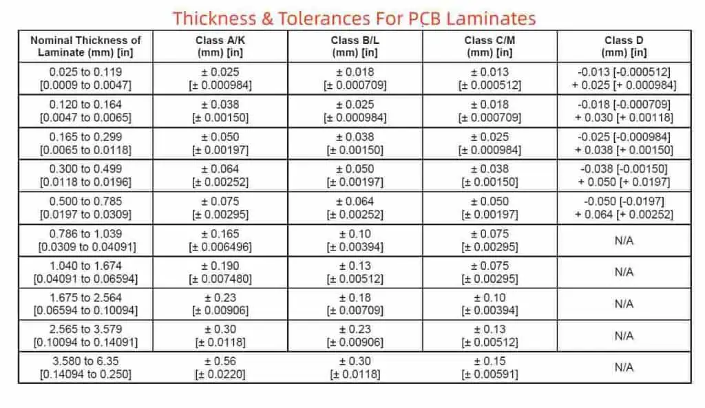
Thickness Tolerances
Standard PCB thickness tolerance is ±10% of the nominal value. However, tolerance can be reduced to ±5% or tighter when holding tight finished thickness is required.
Tighter tolerances often warrant steps like starting with oversized panels and grinding down precisely to achieve specified thickness.
Markings For Thin Boards
For rigid boards under 0.031” thick, fabrication notes indicating “Thin Board” alerts manufacturing processes must delicately handle the thinner material to avoid damage.
Flex Circuits
Flex PCBs involve separate considerations for minimum bend radius, flex layer thickness, stiffener thickness, and other unique constraints.
Consult the Fabricator
To ensure manufacturability and avoid surprises, always review your thickness design requirements with your PCB fabricator early in the design process. An experienced manufacturer can validate your design or suggest improvements.
Conclusion
Designing the optimal PCB thickness requires juggling mechanical, electrical, thermal, fabrication, and cost considerations. Following the guidance in this article will help you select appropriate thicknesses to meet your product needs while enabling efficient manufacturing. Partnering closely with your fabricator is key to optimizing thickness. PCB thickness may seem like a simple issue, but deserves thoughtful design consideration given how foundational it is in determining the quality, cost and performance of the end product.
Frequently Asked Questions
Q: At what point should PCB thickness be considered in the design process?
A: PCB thickness parameters should be estimated starting in the preliminary design stage based on likely layer count, component height, compliance requirements, etc. As the design progresses, thickness can be refined after spacing, stackup, embedded components, and other details are worked out. Consult the fabricator early to validate thickness feasibility.
Q: How does thickness impact the cost of PCB fabrication?
A: Generally, thicker PCBs cost more to fabricate than thinner ones due to increased materials usage. However, ultra-thin boards under 0.020” can also cost more due to additional handling care required. Moderate thicknesses between 0.062” – 0.125” are often the most cost effective.
Q: Can PCB thickness be increased by adding copper rather than dielectric?
A: Yes, thick copper up to 20 mils can be plated onto layers to add rigidity and thickness without impacting dielectric spacing. However, thermal performance diminishes as the board heats up faster due to higher copper content.
Q: What are recommended clearances between components and outer board surfaces?
A: For circuit boards under 24V, a minimum clearance of 0.015” (15 mils) between components and outer surfaces is typical. For higher voltages, greater clearances are advisable, sometimes up to 0.250” (250 mils) or more.
Q: How are very thick PCBs above 0.250” fabricated?
A: Extremely thick boards can be manufactured by laminating separate 0.250” cores together. The individual cores are bonded under high pressure and temperature to form a single thick board ready for further processing. But such thick boards can be challenging to fabricate and often unnecessary.