Introduction
Printed circuit boards (PCBs) have become exponentially more sophisticated over the past decades, transforming from simple single-sided boards to complex multilayer designs pushing the boundaries of materials science and fabrication technologies. This evolution enables PCBs to serve at the heart of today’s electronics innovations from commercial wireless devices to mission-critical aerospace systems. To turn cutting-edge PCB designs into physical reality requires robust, advanced manufacturing capabilities spanning automation, precision processes, testing, and quality control. This article will examine the most advanced PCB manufacturing capabilities defining the current state-of-the-art.
High Density Interconnect (HDI) PCBs

High density interconnect (HDI) PCBs integrate incredibly fine lines and spaces, microvias, and other attributes enabling dense component mounting and multilayer stacking.
Key HDI Capabilities:
- Lines/spaces down to 25μm or less
- Microvias with diameters below 100μm
- Stacked microvia structures
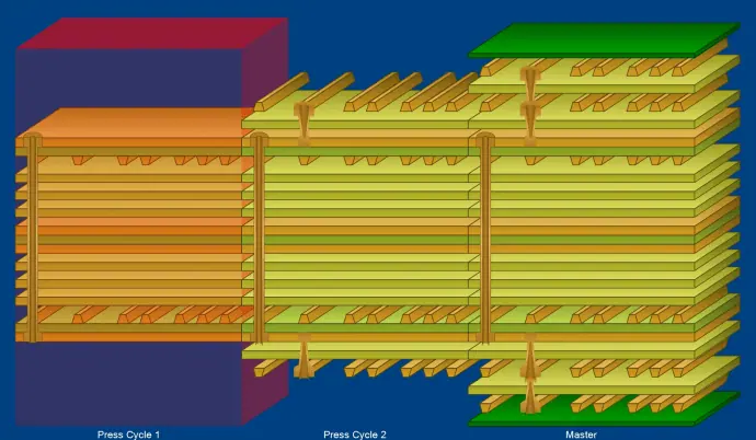
- Sequential lamination with multiple thin cores
- Ultra-thin dielectrics down to 25μm
- Plated laser drilled blind and buried vias
- Build-up layers on outer surfaces
HDI provides the layering that allows complex ICs to interconnect in tiny PCB footprints. The advanced processes, materials, and precision required pushes manufacturing state-of-the-art.
Embedded Passives and Actives

Embedding passive components like resistors and capacitors along with active ICs into the PCB layers conserves space while enhancing electrical performance.
Key Embedded Passive Capabilities:
- Cavity milling and lamination for components
- Tight tolerance passive embedding
- Routing compatibility with buried passives
- Correct dielectric surrounding actives
- Electrical testing of embedded passives
- Thermal management of embedded actives
The processes to reliably integrate actives and passives makes fabrication exponentially more intricate.
Board In Circuit Test (BICT)
Testing the fully loaded board after assembly for correct functionality.
Key BICT Capabilities:
- Robotic handling of assembled boards
- High density bed of nails test fixtures
- Precision landing and contact of test points
- Verification of SMT joints and assemblies
- Detecting faults like opens, shorts, missing parts
- Isolating fabrication vs assembly defects
- Debugging faulty boards by microsectioning and analysis
BICT provides final quality assurance before shipment to customers.
Multilayer Boards >36 Layers
Producing PCBs with layer counts above 36 or even over 60 layers consists of immense manufacturing complexity.
Key Multilayer Capabilities:
- Sequential lamination with multiple thin cores
- Alignment accuracy across dozens of layers
- Via formation through thick cross sections
- Extensive layer registration validation
- Mitigating thin core movement during lamination
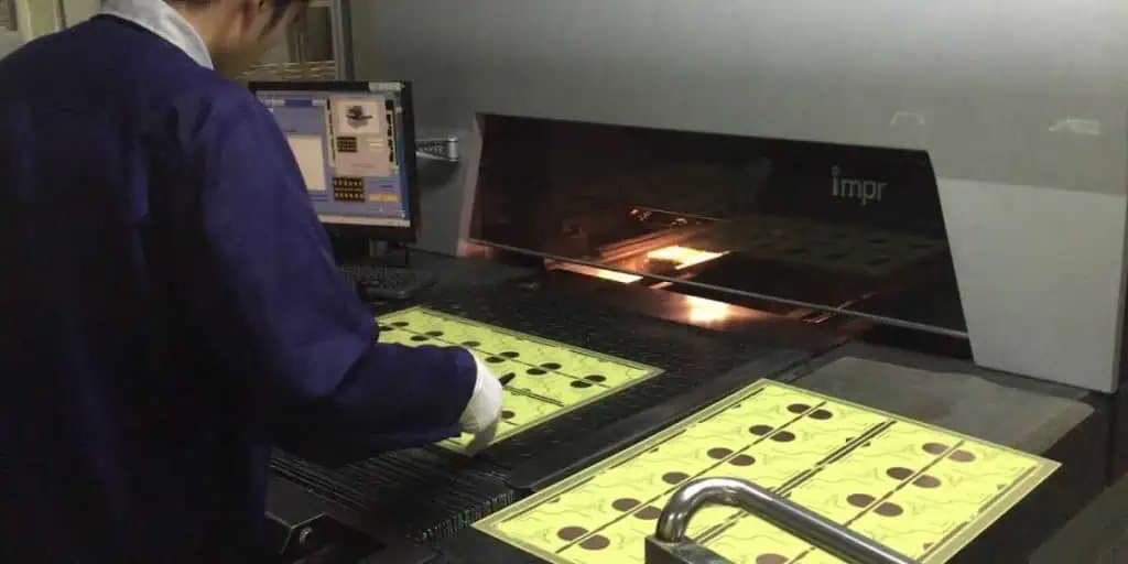
- Balanced press cycles to avoid warp/twist
- Fine pitch microvias for interlayer connections
The precision required to align layers and interconnect vias with minimal defects illustrates masterful process expertise.
Flex and Rigid-Flex PCBs

Flexible PCBs and combinations of flex/rigid enable tight integration in products with dynamic physical demands.
Key Flex/Rigid-Flex Capabilities:
- Thin flexible circuit processing
- Fine space conductors on flex layers
- Coverlayer application and precision
- Bonded inner layer lamination registration
- Surface treatment of flex layer copper
- Conductive adhesive attachments
- Controlled flex layer dimensional stability
- Rigid-flex seam connections
Flex manufacturing necessitates entirely different material expertise than traditional rigid boards.
PCBs > 24” x 24” or Large Format
Producing PCBs with dimensions above 24” x 24” is termed large format fabrication. The sheer size adds complexity across manufacture.
Key Large Format Capabilities:
- Panel size capability greater than 24” x 24”
- Material handling of large panels
- Registration across full panel areas
- Plating tank sizes to accommodate boards
- Special transport and conveyor systems
- AOI inspection scopes with travel range
- Stress-free lamination to prevent warpage
- Thick boards (>0.250”) for rigidity
Successfully fabricating PCBs at such large sizes demands seamless execution.
Higher Frequency PCBs
As digital devices operating frequencies increase into the multi-gigahertz range, PCB substrate properties become increasingly critical.
Key High Frequency Capabilities:
- Tight thickness tolerances and uniformity
- Resin systems with low loss (Dk/Df)
- Smooth copper and low profile surfaces
- Fine features and spacing
- Advanced simulation and analysis
- Methodologies for signal path isolation
- Attention to dielectric properties
- Thin laminates and dielectrics
- Copper roughness treatments
Achieving smooth signal transfers at high frequencies requires precision engineering of materials, stackups, and geometry.
Aluminum-Based PCBs
Replacing standard FR4 materials with aluminum or other metal core substrates provides exceptional thermal performance.
Key Metal Core Capabilities:
- Thermal bonding with thin dielectric layers
- Metal substrate surface preparation
- Thermal coefficient of expansion control
- Thermal management features like flatness, hardness, and via conduction
- Dielectric selection for metal adhesion and ruggedness
- Higher temperature processes
- CTE matched component assembly
- Thermally conductive finishes
Metal core PCBs operate robustly in extreme thermal environments.
Direct Imaging (LDI)
Laser direct imaging replaces standard lithographic methods for forming ultra-fine conductors down to 10μm or less.
Key Laser Imaging Capabilities:
- Laser imaging resolution of 10μm or finer
- Precise depth of focus on uneven surfaces
- Layer to layer alignment precision
- Seamless integration across design-fabrication workflow
- High speed imaging for productivity
- Scalable and lower maintenance than optical
- Real-time image adjustments during exposure
LDI enables next-generation PCB geometries impossible with legacy fabrication phototools.
Additive Processes

Additive methods like inkjet printing are beginning to complement or replace conventional subtractive PCB processing.
Key Additive Process Capabilities:
- Inkjet solder mask, legend, and markings deposition
- Print-n-peel temporary masks for etching
- Direct copper printing on substrates
- Printed dielectric and conductive adhesives
- Rapid prototyping of traces
- High mix/low volume customization
- Reduced chemical waste versus subtractive
- Finer resolution than standard methods
Additive techniques enable new environmentally friendly fabrication work flows.
Conclusion
This overview of advanced PCB manufacturing capabilities illustrates the tremendous innovations propelling the industry forward. From exponential densification to embedding actives inside the layers, fabricating the PCBs that underpin emerging technologies involves immense expertise and process mastery. Through continual development of these sophisticated manufacturing capabilities, PCB fabricators enable designers to turn visions of cutting-edge electronic devices into reality. The future will certainly bring a new realm of techniques allowing PCBs to progress supporting society’s growing technological demands.
Frequently Asked Questions
Q: What are some emerging HDI technologies on the horizon?
HDI continues advancing with thinner dielectrics, smaller microvias, printed embedded passives, sequential laminations, increased layer counts, and improved modeling – enabling further component densification. Laser direct imaging down to 5um lines will enable finer densities.
Q: What limits manufacturing capabilities for higher frequency PCBs?
At high frequencies, inconsistencies in dielectric thickness, copper surface roughness, resin purity, glass weave, lamination pressure, and other variables degrade performance. Each process must be tightly controlled to avoid signal losses.
Q: What are some challenges when embedding actives in PCBs?
Embedding actives introduces fabrication intricacy in cavity formation, dielectric material selection, thermal dissipation, electrical interconnect, reworkability, signal isolation and simulation. As more actives are embedded, the manufacturing expertise required also increases.
Q: How are very small microvias formed?
Laser drilling is required for microvias under 8 mils diameter. Laser produces clean, precise holes versus mechanical drilling even through complex layer stacks. Tight process controls are needed for capturing via depths accurately.
Q: What are key differences when manufacturing large format PCBs?
Challenges arise in handling large, thin panels across processes. Alignment and registration becomes exponentially more difficult at large sizes. Thermal stress and warp control is crucial. Conveyor widths, tank sizes, lamination presses and other equipment must be scaled up.
