Top 12 Electronic Prototype Manufacturers In China

Electronic Prototyping Company

Introduction

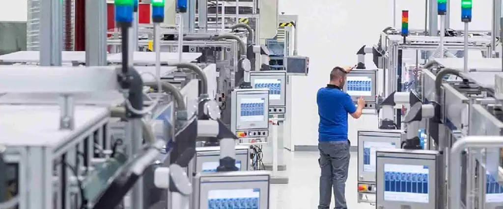
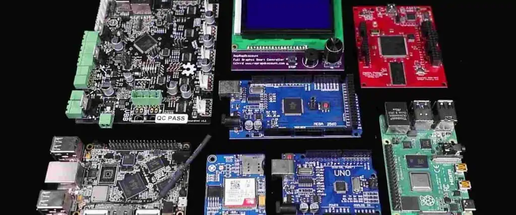
China has become a leading hub globally for electronics manufacturing services including prototype engineering and low volume production. The availability of skilled engineers, advanced manufacturing infrastructure and competitive costs has attracted many multinational OEMs, startups and design houses to source electronics prototyping in China.

This article profiles the top 12 electronic prototype manufacturers in China who deliver advanced capabilities, quality and rapid turnaround for NPI (new product introduction) engineering.

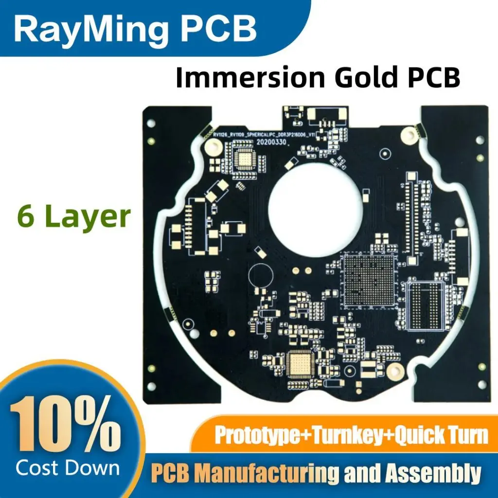
1. RayMing Technology

RayMing is an ISO 13485 and ISO 9001 certified company focused on fast turnkey prototyping of electronic devices. With over 200 engineers and three manufacturing facilities, they deliver advanced capabilities across PCB design, component engineering, enclosure design, firmware development and testing services.

Location: Shenzhen, China

Services:

  • PCB Design – Up to 16 layer boards
  • Component Engineering
  • Enclosure – Plastic and metal
  • Prototype Assembly
  • Testing including EMC/RF
  • Firmware and software
  • Complete product engineering

Industries Served:

Customers: Startups, OEM R&D teams, design houses in North America and Europe

Key Differentiators:

  • One stop shop for electronic product engineering
  • Both in-house capabilities and partner network
  • Design for manufacturing expertise
  • Focus on quality and product safety

Certifications: ISO 13485, ISO 9001, UL

Consumer Electronics Assembly

2. StarLink Electronics Technology

StarLink provides rapid prototyping and electronics engineering services to help companies launch products faster. With over 500 engineers and 14 years of experience supporting startups, they deliver functional prototypes meeting quality and reliability needs.

Location: Zhuhai, China

Services:

  • PCB Development
  • Mechanical Engineering
  • Prototype Manufacturing
  • Product Testing

Industries Served:

  • Consumer Electronics
  • Automotive Electronics
  • Industrial Electronics
  • Medical Electronics

Customers: Startups, medium/large companies in North America and Europe

Key Differentiators:

  • Rapid prototype delivery in 7-15 days
  • One stop engineering capabilities
  • Scalable volume production
  • Strong focus on quality

Certifications: ISO 9001, ISO 14001, QC 080000

3. Wispro Technology

Wispro provides electronic product design, prototyping and manufacturing services. With 700+ employees, they deliver high quality prototypes and low volume production using advanced technologies.

Location: Shenzhen, China

Services:

  • Product Design – Mechanical, Electrical, Software
  • PCB Layout
  • Prototype Fabrication
  • Low Volume Manufacturing
  • Testing Services

Industries Served:

  • Consumer Electronics
  • Wireless Communications
  • Industrial Controls
  • IoT Products
  • Automotive Electronics

Customers: Multinational companies, startups, design houses

Key Differentiators:

  • 28 years of experience supporting electronics OEMs
  • High quality prototypes with quick turnaround
  • Seamless transition to production
  • Rigorous quality systems

Certifications: ISO 9001, ISO 14001, ISO 13485

4. Libing Technology

Libing provides professional one-stop engineering services focused on electronic product design and manufacturing. With over 200 employees and 10 years of experience, they deliver reliable high-tech solutions.

Location: Shenzhen, China

Services:

  • Electronics Design
  • Mechanical Engineering
  • PCB Layout
  • Firmware Development
  • Prototype Building
  • Pilot Manufacturing

Industries Served:

  • Industrial Equipment
  • Measurement Instruments
  • LED Lighting
  • Automotive Electronics
  • IoT Products

Customers: Startups, small and mid-sized brands based in North America and Europe

Key Differentiators:

  • High quality deliverables with effective design for manufacturing
  • Supply chain management capabilities
  • Ability to seamlessly scale up to production
  • Comprehensive project management

Certifications: ISO 9001, ISO 14001

Electronics panel board manufacturers

5. Advanced Assembly

Advanced Assembly provides rapid prototyping of electronic devices with a focus on assembling and testing prototypes. They leverage an international supply chain to procure components and build prototypes.

Location: Shenzhen, China

Services:

Industries Served:

  • Consumer Electronics
  • Industrial Equipment
  • Automotive Electronics
  • IoT and Home Automation
  • LED Lighting

Customers: Startups, makers, and electronics companies worldwide

Key Differentiators:

  • Specialization in assembling fully functional prototypes
  • Flexible and fast turnaround times
  • International component sourcing
  • Convenient online order placement and tracking

Certifications: ISO 9001

6. OurPCB Tech

OurPCB provides fast PCB prototyping as well as electronics assembly. They have instant online quoting and order placement for PCB fabrication and assembly with flexible quantity.

Location: Shenzhen, China

Services:

  • 24 Hour PCB Prototypes
  • SMT Assembly
  • PCB Component Procurement
  • Functional Prototype Building

Industries Served:

  • Consumer Electronics Makers
  • Maker Community
  • Small Businesses
  • Education and R&D

Customers: Startups, makers, hackers, students and electronics enthusiasts globally

Key Differentiators:

  • Instant 24 hour PCB prototype service
  • Online order placement and tracking
  • Flexible order quantities
  • Cost effective solutions

Certifications: ISO 9001

7. JZJ PCB

JZJ PCB provides advanced PCB prototype services as well as electronics manufacturing. They have 16 years of experience focused on meeting prototyping needs for innovators worldwide.

Location: Jiangmen, China

Services:

  • Multilayer PCB Prototypes
  • SMT Assembly
  • Sheet Metal Fabrication
  • Functional Prototype Building

Industries Served:

  • Consumer Electronics
  • Industrial Automation
  • Automotive Electronics
  • Medical Equipment

Customers: Startups, makers, and electronics innovators globally

Key Differentiators:

  • High quality multilayer PCB prototypes
  • Flexible order quantities
  • Design for manufacturing services
  • Seamless transfer to production

Certifications: ISO 9001, ISO 14001, UL

8. Wellpcb Technology

Wellpcb offers advanced PCB prototyping capabilities using high end manufacturing equipment. They provide engineering services to support all phases of electronic product development.

Location: Dongguan, China

Services:

  • Multilayer PCB Prototypes – up to 16 layers
  • HDI PCBs
  • Flexible PCB Circuits
  • PCB Component Selection and Sourcing
  • DFM Analysis

Industries Served:

  • Consumer Electronics
  • Automotive
  • Industrial Equipment
  • Medical Devices

Customers: Electronics manufacturers, OEM R&D teams, product design companies

Key Differentiators:

  • Advanced PCB technology – SLP, any-layer HDI, Flex-rigid
  • Strong engineering capabilities
  • Inventory of components for prototyping
  • Seamless transfer to volume production

Certifications: ISO 9001, ISO 14001, IATF 16949

9. Amitron

Amitron delivers electronics engineering design including PCB layout, simulation, mechanical design and prototyping services to customers globally.

Location: Shenzhen, China

Services:

  • PCB Design Services
  • PCB Simulation and Analysis
  • Electronic Product Design
  • Mechanical Engineering Design
  • Prototype Fabrication

Industries Served:

  • Industrial Equipment
  • Consumer Electronics
  • Automotive
  • Medical Devices

Customers: Small and mid-sized electronics companies, startups, makers

Key Differentiators:

  • Advanced engineering capabilities and expertise
  • Strong focus on electronics reliability
  • Experience supporting a wide range of industries
  • End-to-end product development services

Certifications: ISO 9001

10. PCB Masters

PCB Masters provides professional engineering support for PCB prototyping along with design for manufacturing analysis. Their capabilities support faster development of electronic devices.

Location: Shenzhen, China

Services:

  • PCB Design Services
  • PCB Prototype Fabrication
  • Component Engineering
  • PCB DFM and Analysis
  • PCB Testing Services

Industries Served:

  • Industrial Controls
  • Consumer Electronics
  • Automotive Electronics
  • IoT Products

Customers: Electronics manufacturers, startups, makers

Key Differentiators:

  • 20 years experience in PCB engineering services
  • Adherence to IPC standards
  • Strong PCB design expertise
  • Seamless transfer to production

Certifications: ISO 9001

through-hole assembly process

11. JingHongYiDa

JingHongYiDa provides specialized electronics engineering services focused on supporting product design and prototyping. Their capabilities help accelerate time-to-market.

Location: Shenzhen, China

Services:

  • Electronics Product Design
  • PCB Layout
  • Mechanical Engineering
  • Firmware Development
  • Prototype Fabrication

Industries Served:

  • Consumer Electronics
  • Industrial Equipment
  • Automotive Electronics
  • IoT Products
  • Medical Devices

Customers: OEM R&D teams, startups, makers, design houses

Key Differentiators:

  • Multidisciplinary engineering capabilities
  • Experience transitioning prototypes to production
  • Rigorous quality control practices
  • Bilingual team for good communication

Certifications: ISO 9001, ISO 14001

12. Shenzhen Limei Electronics

Limei provides specialized electronics manufacturing services focused on supporting engineering teams with PCB fabrication and assembly. Their capabilities help accelerate prototyping.

Location: Shenzhen, China

Services:

  • PCB Prototype Fabrication
  • PCB Assembly Services
  • Functional Testing
  • Component Procurement
  • New Product Introduction

Industries Served:

  • Consumer Electronics
  • Industrial Equipment
  • Automotive Electronics
  • Medical Devices

Customers: OEM engineering teams, startups, design houses

Key Differentiators:

  • 15+ years experience supporting prototype builds
  • Small and mid-size orders accommodated
  • Multiple quality certifications
  • Convenient order tracking system

Certifications: ISO 9001, ISO 14001, ISO 13485

Conclusion

China offers a wide range of capable electronics manufacturing services companies to partner with for engineering and prototyping new electronic devices. They provide advanced expertise, rapid turnaround, and competitive costs to help innovators accelerate product development. With stringent quality systems, international sourcing and experience transitioning to production, they enable streamlined new product introduction. Global OEMs, startups and entrepreneurs are leveraging these expert Chinese prototyping partners to bring their electronics innovations to market faster.

Frequently Asked Questions

Q1: What are some of the benefits of prototyping electronics in China?

Some key benefits are:

  • Access to skilled, low cost engineering talent
  • Mature component supply chains
  • Advanced manufacturing technologies
  • Ability to scale to high volume production
  • Cultural understanding of local Chinese market
  • Cost savings compared to domestic US or Europe prototyping
  • Convenient time zones for communication

Q2: What due diligence should be done before selecting an electronics prototyping partner in China?

Important factors to consider in selection process:

  • Review their design capabilities, expertise and past projects
  • Evaluate their quality certifications and processes
  • Ensure they have good security and IP protection
  • Check lead times, minimum order quantities
  • Validate responsive communication channels
  • Request customer references to check satisfaction
  • Review their component sourcing abilities
  • Audit their manufacturing setup if possible
  • Align on project requirements like documentation, DFM, inspection testing needed

Why use Black PCB for electronic device ?

BLACK PCB

In the world of electronics manufacturing, the choice of Printed Circuit Board (PCB) color is more than just an aesthetic decision. While green PCBs have long been the industry standard, black PCBs are gaining popularity for their unique advantages. This article delves into the world of black PCBs, exploring their benefits, applications, and why they might be the right choice for your next electronic project.

1. Introduction to Black PCBs

1.1 What is a Black PCB?

A black PCB is a printed circuit board that uses a black solder mask instead of the traditional green. The solder mask is the thin layer of polymer that covers the copper traces on a PCB, protecting them from oxidation and preventing solder bridges during assembly.

1.2 The Rise of Black PCBs

In recent years, black PCBs have seen a surge in popularity, particularly in high-end consumer electronics, automotive applications, and specialized industrial equipment. This trend is driven by both aesthetic and functional considerations.

2. Advantages of Black PCBs

Black PCBs offer several distinct advantages over their green counterparts, making them an attractive option for many applications.

2.1 Enhanced Heat Dissipation

One of the most significant benefits of black PCBs is their superior heat dissipation properties. The black color absorbs and radiates heat more effectively than lighter colors, potentially leading to better thermal management in electronic devices.

2.2 Improved Contrast for Inspection

Black solder mask provides excellent contrast against copper traces, component markings, and solder joints. This high contrast makes visual inspection easier and more accurate, potentially reducing assembly errors and improving quality control processes.

2.3 Aesthetic Appeal

In an era where product design is increasingly important, black PCBs offer a sleek, modern appearance. This can be particularly valuable in consumer electronics where the PCB might be visible through transparent or translucent casings.

2.4 Reduced Light Reflection

Black PCBs reflect less light than their lighter-colored counterparts. This property can be crucial in applications where stray light reflection could interfere with optical sensors or other light-sensitive components.

2.5 Enhanced Durability

Some manufacturers claim that black solder mask can offer improved durability and resistance to environmental factors compared to traditional green solder mask.

Read more about:

3. Applications of Black PCBs

The unique properties of black PCBs make them suitable for a wide range of applications across various industries.

3.1 Consumer Electronics

High-end smartphones, laptops, and gaming consoles often use black PCBs for their aesthetic appeal and thermal properties.

3.2 Automotive Electronics

The automotive industry is increasingly adopting black PCBs in dashboard displays, infotainment systems, and under-hood electronics due to their heat dissipation properties and durability.

3.3 Aerospace and Defense

Black PCBs are finding applications in aerospace and defense equipment, where their heat management properties and reduced light reflection can be advantageous.

3.4 Industrial Control Systems

In industrial settings, black PCBs are used in control systems and monitoring equipment, where their ease of inspection and durability are valuable assets.

3.5 LED Lighting

The heat dissipation properties of black PCBs make them an excellent choice for LED lighting applications, particularly in high-power or compact designs.

4. Manufacturing Process of Black PCBs

The manufacturing process for black PCBs is similar to that of traditional PCBs, with a few key differences.

4.1 Material Selection

The base material for black PCBs is typically the same as for other PCBs, usually FR-4 (a glass-reinforced epoxy laminate). The key difference lies in the solder mask.

4.2 Solder Mask Application

The black solder mask is applied using similar techniques to green solder mask, such as screen printing or photoimaging. However, achieving a uniform, deep black color can be more challenging and may require specialized formulations.

4.3 Curing Process

After application, the black solder mask undergoes a curing process, typically involving UV exposure and heat treatment. This process may need to be carefully controlled to ensure the desired color and properties are achieved.

4.4 Quality Control

Quality control for black PCBs may involve additional steps to ensure color consistency and check for any defects that might be more visible against the black background.

5. Challenges and Considerations

While black PCBs offer many advantages, there are also some challenges and considerations to keep in mind.

5.1 Cost Implications

Black PCBs may come at a premium compared to traditional green PCBs due to the specialized materials and potential additional processing steps required.

5.2 Heat Absorption in Certain Environments

While the heat dissipation properties of black PCBs can be advantageous, in some environments, the increased heat absorption could potentially lead to higher operating temperatures if not properly managed.

5.3 Visibility of Certain Components

Some components or markings might be less visible against a black background, potentially requiring adjustments in assembly or inspection processes.

5.4 Limited Availability

Not all PCB manufacturers offer black solder mask options, which could limit sourcing options for some projects.

6. Black PCBs vs. Traditional Green PCBs

To fully appreciate the impact of black PCBs, it’s essential to compare them directly with traditional green PCBs.

6.1 Thermal Performance

Black PCBs generally offer better heat dissipation compared to green PCBs, which can be crucial in high-power or compact designs.

6.2 Visual Inspection and Assembly

The high contrast provided by black PCBs can make visual inspection easier compared to green PCBs. However, this may vary depending on the specific components and markings used.

6.3 Aesthetic Considerations

Black PCBs offer a more modern, sleek appearance compared to the traditional look of green PCBs. This can be a significant factor in consumer electronics and other visible applications.

6.4 Cost Comparison

Black PCBs typically come at a higher cost compared to green PCBs due to the specialized materials and potential additional processing steps.

6.5 Industry Adoption

While green PCBs still dominate the market, black PCBs are gaining ground, especially in specific sectors like high-end consumer electronics and automotive applications.

7. Future Trends in Black PCB Technology

The future of black PCB technology looks promising, with several emerging trends:

7.1 Advanced Materials

Research is ongoing to develop black solder mask materials with improved properties, such as enhanced thermal conductivity and durability.

7.2 Integration with Flexible and Rigid-Flex PCBs

As flexible and rigid-flex PCBs become more prevalent, we can expect to see black solder mask options for these advanced board types.

7.3 Improved Manufacturing Processes

Advancements in manufacturing processes may lead to more consistent and cost-effective production of black PCBs.

7.4 Customization and Branding Opportunities

The use of black PCBs may open up new possibilities for customization and branding, such as laser etching or printing vibrant colors on the black background.

7.5 Sustainability Considerations

Future developments may focus on creating more environmentally friendly black solder mask materials, aligning with the growing emphasis on sustainability in electronics manufacturing.

8. Choosing Between Black and Green PCBs

When deciding between black and green PCBs for your project, consider the following factors:

8.1 Application Requirements

Consider the specific requirements of your application, such as thermal management, light reflection, and visibility needs.

8.2 Design Aesthetics

If the PCB will be visible in the final product, the aesthetic appeal of black PCBs might be a deciding factor.

8.3 Budget Constraints

Weigh the potential benefits of black PCBs against their higher cost to determine if they fit within your project budget.

8.4 Manufacturing Capabilities

Ensure that your chosen manufacturer has experience and capabilities in producing high-quality black PCBs.

8.5 Industry Standards and Expectations

Consider any industry-specific standards or expectations that might influence the choice between black and green PCBs.

Conclusion

Black PCBs represent an exciting development in the world of electronics manufacturing. Their unique properties, including enhanced heat dissipation, improved contrast for inspection, and aesthetic appeal, make them an attractive option for a wide range of applications. While challenges exist, such as higher costs and potential limitations in certain environments, the benefits of black PCBs often outweigh these considerations in many modern electronic designs.

As technology continues to advance and the demand for high-performance, visually appealing electronics grows, we can expect to see further innovations in black PCB technology. Whether you’re designing cutting-edge consumer electronics, robust industrial control systems, or next-generation automotive components, black PCBs offer a compelling alternative to traditional green boards.

Ultimately, the choice between black and green PCBs will depend on the specific requirements of your project. By carefully considering the advantages, challenges, and future trends associated with black PCBs, you can make an informed decision that balances performance, aesthetics, and cost-effectiveness in your electronic designs.

What is Prepreg in PCBs?

PREPREG pcb

Introduction

Prepreg, also referred to as pre-impregnated composite fibers, is a key material used in the manufacture of multilayer printed circuit boards (PCBs). It is a fibrous reinforcement that has been pre-impregnated with a resin system prior to laminating PCB layers together.

Prepregs provide electrical isolation between the conductive copper layers in a PCB while also offering mechanical stability. They impart crucial properties like dimensional stability, bond strength, heat resistance and dielectric performance. Selecting the right prepreg material is critical for the reliability of multilayer PCBs used in electronics.

This article provides an overview of PCB prepregs covering their composition, properties, types, role in the PCB fabrication process and methods for quality control testing.

Composition of PCB Prepregs

Prepregs used for PCB fabrication are generally composed of:

  • Fiberglass fabric reinforcement
  • Epoxy or other polymer resin systems
  • Filler particles like silica
  • Catalysts and accelerators
  • Flame retardants

Fiberglass Fabric

The fiberglass fabric provides mechanical strength and dimensional stability. Some types used are:

  • 108, 211 fiberglass with 5-15 ฮผm diameter fibers
  • Woven fabric with different weave styles
  • Non-woven random fiber mats

Resin System

The resin coats and bonds together the fibers. Different resin types used are:

  • Epoxy โ€“ Most common for FR-4 grade prepregs
  • Polyimide โ€“ For high temperature PCBs
  • BT (Bismaleimide Triazine) โ€“ Low moisture absorption
  • Cyanate ester โ€“ High frequency, low loss PCBs

Fillers

Fillers like fused silica reduce the coefficient of thermal expansion (CTE) of the composite to match copper. They also control flow, adhesion, thermal conductivity and cost.

Other Components

Small amounts of curing agents, accelerators, flame retardants and other additives tailor the prepreg properties.

Properties of PCB Prepregs

Prepreg 1080
Prepreg 1080

Desirable properties in prepregs for quality PCBs:

Dielectric Constant – Stable dielectric constant and low dissipation factor for high frequency performance. Values of 3.5-5 typical for glass fabric-epoxy prepregs.

Dimensional Stability – Low Z-axis shrinkage and expansion under temperature cycling to avoid via failures. Typical X-Y shrinkage < 0.5%.

Bond Strength – Strong adhesion to copper foils and between prepreg layers with good resistance to delamination. Bond strength > 2.5 N/mm.

Decomposition Temperature – High Td above 300ยฐC indicates stable thermal performance and prevents charring issues.

Moisture Absorption – Low affinity for moisture prevents electrical leakage and reliability issues due to vapor pressures. <0.5% uptake standard.

Flow and Filler – Adequate resin flow to fill irregularities but not excessive to avoid shorts between conductors. Filler loading around 15-40%.

Flame Retardancy – High degree of flame resistance with resistance to ignition, burning and smoke generation. UL 94 V-0 rated material.

Types of PCB Prepregs

Many varieties of prepregs cater to different PCB performance requirements:

TypeKey Characteristics
FR-4 EpoxyMost widely used. Good processability. Low cost. Temperature rating 130ยฐC (Tg 135-155ยฐC)
High Tg EpoxyTg > 170ยฐC for higher heat resistance. Ex: BT epoxy, Allied Signal Arlon 85N
PPO (Polyphenylene oxide)Low loss and stable Dk for RF/microwave. Improved Z-axis CTE. Ex: Rogers TMM 10i
Cyanate EsterLowest loss, tightly controlled Dk for high freq. Ex: Taconic TacPreg CE
PTFE CompositeExtremely low Dk ~2.2. Low loss. Ex: Rogers RO3003
PolyimideVery high Tg >240ยฐC, low Z-axis expansion. Ex: DuPont Kapton VN, Hitachi PI-2525
Non-woven AramidHigh bond strength. Low CTE for large boards. Ex: Isola Preperm P92

The choice depends on thermal, electrical and high frequency requirements.

Role of Prepreg in PCB Fabrication

Prepreg performs several crucial functions in the PCB fabrication process:

1. Bonding Layers

Prepreg is used to bond the inner copper layers into a multilayer board through lamination under heat and pressure.

2. Electrical Isolation

It provides electrical isolation between two conductive copper sheets or internal planes while still allowing conduction through drilled holes.

3. Inner Layer Core

Prepreg-copper sheets also serve as the starting cores during the layup of multilayer PCBs.

4. Serving Solder Mask

Special prepreg with photo-sensitive resin can act as the solder mask layer on outer surfaces.

5. Imparting Rigidity

The composite material lends mechanical strength and rigidity to the PCB structure.

6. Controlling Z-axis CTE

Low expansion prepregs control growth along thickness to avoid reliability issues.

7. Providing Heat Resistance

High Tg prepregs allow PCB operation at elevated temperatures.

8. Establishing Dielectric Constant

The resin-fiber matrix governs the dielectric constant of the insulating PCB layers.

PCB Prepreg Handling Considerations

To maintain quality, prepregs require careful handling:

  • Prepregs are supplied sealed in polythene bags to prevent moisture absorption. Unused prepreg should be resealed immediately.
  • Storage temperature should be 18-25ยฐC. Freezing conditions can ruin the material while excessive heat can cause partial curing.
  • Shelf life is typically 1 year at 23ยฐC. Prepregs should be used on a FIFO basis before expiry.
  • Allow refrigerated prepreg to reach room temperature before opening to prevent moisture condensation.
  • Avoid excessive exposure to UV light which can initiate polymerization. Use under yellow light.
  • Use clean lint-free gloves when handling to avoid contamination of the tacky surfaces.

Proper prepreg handling as per manufacturer guidelines ensures consistent performance.

PCB Prepreg Testing

Some key tests carried out on prepreg materials for quality control are:

Resin Flow Testing

  • Resin viscosity measured at standard temperature and pressure
  • Tested after partial curing for specified duration
  • Ensure adequate but controlled flow during lamination

Gel Time Test

  • Monitoring resin polymerization at set temperature
  • Inflection point taken as gel time
  • Checks adequate processing window before curing

Differential Scanning Calorimetry

  • Monitors heat flow versus temperature to detect transitions
  • Gives resin glass transition temperature, cure peaks
  • Indicates degree of curing with heat ramps

Dielectric Constant

  • Measured over frequency range like 10 MHz โ€“ 10 GHz
  • Indicates electrical insulation capability
  • Stable value desired through frequency spectrum

Flammability Testing

  • UL 94 vertical burning test rating for flammability
  • High priority for safety critical PCB applications

Prepreg received from supplier is also tested before PCB usage.

Conclusion

Prepreg forms the fundamental dielectric building block of multilayer PCBs that electrically isolates the conductive layers while also imparting mechanical strength. The composition of the resin, fabric reinforcement and fillers that make up prepreg governs the thermal, electrical and reliability performance of the PCB. With the diversity of prepreg types available, PCB manufacturers can select the optimal material suited for their performance requirements and process compatibility. Strict handling and quality control measures for prepreg also minimize variability and ensure consistent results during PCB fabrication. As PCBs become thinner and operate at higher frequencies and temperatures, engineering the prepreg materials is critical for enabling their miniaturization and reliability.

Frequently Asked Questions

Q1. How does prepreg material selection influence the fabrication process of multilayer PCBs?

Some ways prepreg properties affect multilayer PCB fabrication are:

  • Flow viscosity during lamination cycle time and temperature
  • Tg impacts the curing required and potential rework
  • Low thermal expansion suits large area boards
  • High filler suits complex topographies
  • Adhesion levels affect press parameters
  • Moisture sensitivity influences handling
  • Dielectric properties affect impedance control

Q2. What are some troubleshooting tips for issues with PCB prepreg?

Troubleshooting tips for prepreg related PCB issues:

  • Delamination or blistering – Poor adhesion, high moisture absorption
  • Cracking or crazing – Excessive resin flow, filler settlement
  • Poor dimensional stability – High Z-axis CTE material
  • Wicking or shorts – Insufficient resin viscosity
  • High dielectric constant – Incompatible resin system
  • Poor heat resistance – Low Tg material used

So proper prepreg selection, handling and process controls are vital.

Difference between PCB Core and Prepreg Materials

Prepreg Core is the isolating material of the PCB, often referred to as before laminating. Manufacturers mostly use Prepreg as a binding substance. Not just that, experts also employ it as a multifunctional PCB inner conduction material. Thus, once the user laminates the Prepreg & extrudes the half-healed epoxy, it solidifies and runs and binds the multilayer panels together to create a dependable insulator.

When the distinction between both Core and Prepreg is evident, what specific property should you use? When plate, etching, and drying, how do crucial electrical characteristics change? As more manufacturers are aware of the work at GHz frequency range, these principles are vital to size traces of these materials appropriately and prevent difficult signal integrity difficulties.

WHAT IS PREPREG MATERIAL?

Prereg PCB is a conductive substance that planners pack to provide the appropriate insulate between the copper and a core or dual Core of a PCB. Prereg is a level of isolation. Since a copper sheet and a core may be bonded, it may be called a binding material safely. Users may also customize Prereg as special insulators to their demands. A chemical technique may also be used to turn a given section of a Prereg into a conducting zone by combining appropriate catalytic substances and additives.

WHAT IS PCB CORE MATERIAL?

PCB CORE VS PREPREG MATERIALS

The PCB core is a hard foundation material coated on one or two aspects with copper. The CORE is employed in the fabrication of single-sided and two-sided boards and in the manufacture of PCBs of sharing arrangements.

The PCB center consists of the FR4 elements of titanium epoxy laminates and copper traces. The Prereg connected the layers and the PCB core when users heated there.

Experts responded to the Core as the core panel and also to the Core of PCB production. It has a certain copper, width, and firmness of double bread. Its multilayer board is a mixture of Prereg and Core.

HOW IS PREPREG MADE?

Prepreg is a fiberglass fabric/towel coated with a resin preservative, as the name implies. The glass strands are knitted into a glass tissue. This glass fiber fabric is half-dried into material from the B-stage.

Most prepregs are substances of the B-stage. It is vital to track the volume fraction of the material used throughout the production process Prepreg, as it enables the material to be adjusted according to the demand. The number of repetitions of warp and fill affects the epoxy the glass weave can hold.

HOW WE CAN CHOOSE PREPREG MATERIAL:

FULL PCB MANUFACTURING Quote

Depending on the size and other needs, many kinds of prepregs are integrated into PCBs. According to its resin composition, Prepregs are compatible with standard resin (SR), mid resin (MR), or high resin (HR). The more and more resin it holds, the more costly it becomes.

CORE AND PREPREG MATERIALS:

With clear structural differences in the core prepreg materials, it is critical from a circuit design perspective to get an exact value for the electrical conductivity and the return loss. If your signals have minimal growth time, you can usually get away using a user information sheet value. Once your knee and analog signals have reached the GHz range, attention must be taken with the datasheet values, particularly when modeling interconnect behavior and employing resistance-controlled routing.

The difficulty with data source numbers is that the true electrical conductivity determined is based on the test technique, geometric routing, particular frequencies, convention on the law, and the thickness of the material. John Coonrod spoke extensively about this subject in a recent interview. The fabric pattern of PCB core/prepreg components renders them inhomogeneous and anisotropic, meaning that the main material qualities change in space and various directions. This is why we get fiber weaving phenomena such as excitation of the skew and fiber cavity.

You could wonder, why should a laminate density define the material characteristics? The reason is that the important parameter characterizing the signal behavior is a useful electrical conductivity, which relies on your material’s trace size and layer thickness. 

Finally, copper texture on a particular laminate is the second key characteristic to be considered. The above two studies Will present efficient dielectric constant calculations for the geometries of microstrip and strip lines without the assumption of copper ruggedness. There is, however, a straightforward linear approach to compensate for copper rawness:

Suppose you are working at really high speeds and high frequencies and want very precise connection characterization. In that case, the best choice is to produce a test coupon and utilize standard measurements to calculate the functional dielectric constant. A topology that roughly resembles your anticipated interconnection geometry should be used in your test procedure. This requires some effort at the front, but precise testing and measuring might save you needless prototype runs in the rear.

Suppose you pick from a variety of PCB core versus prepreg material, the Altium Designer.   You will have access, or you may define special material characteristics for exotic substrates, to a component library that offers crucial information on various standardized materials. These capabilities enhance your efficiency and enable you to adjust your design to very particular applications.

THE DIFFERENCE BETWEEN PCB CORE VS PREPREG:

PCB cores and coatings are comparable yet extremely distinct in certain aspects. Your Core is one or more prepreg panels crushed, hardened, and heat-cured, and the Core is covered on each side with a copper foil. The resin is injected with the prepreg material, wherein the resin is solidified but left untreated. Many companies define Prepreg as the duct tape that ties the core components together; the exposure to heat allows the resin to start binding to the next layers when 2 cores are placed at either edge of a prepreg lamellate. The solidified resin cures slowly bypass, and its resultant material characteristics approximate the core layers.

The resin substance contains a glass fabric. The production procedure for this glass fabric is quite similar to that for the fabrication of yarns. The glass fabric may be pretty narrow (e.g., 7638 prepreg) or flexible (e.g., 1081 prepreg), manufactured by the weaver. Any flaws and general yarn uniformity will decide the magnetic characteristics responsible for the scatter, loss, and fiber tissue impact of the signals in the circuit.

According to the resin amount, resin variety, and glass fabric, core PCB vs. prepreg materials may have a slightly differing refractive index. This may be a concern if boards need to be designed that match extremely exact impedances since the absorption coefficient observed on a track relies on the dielectric constants of the material resulting. Not even all prepreg and core materials are mutually compatible, and core/prepreg stacks with widely varying dialectal constants make predicting accurate dielectric constants and inefficiencies in an interconnection problematic.

Every PCB core or prepreg material has a problem with high voltage creeping and leakage current. Copper electromigration and further expansion of conductive filaments are a cause for the FR4 material creeping criteria. This difficulty drove a move to โ€“ anti (Non-DICY) in FR4 Prepreg and coatings, albeit with a want to improve the transition of the glass and breakdown temperatures. Phenolic resins offer greater breakdown and transition temperatures than DICY resins and increase isolation resistance upon complete curing.

We can interpret it this way, and The Prepreg is a PCB isolating material. Prepreg shall not be Prepreg before encapsulation, also known as Prepreg. It shall be utilized mainly as a connecting material and an isolating material for a multilayer integrated circuit board’s inner guiding pattern. After lamination, the semi-curated epoxy is ejected, starts to flow, reinforces the multilayer sheets, and produces a durable insulator.

The Core is the essential material for the production of PCB. The Core is also referred to as the core panel, which has some toughness, depth, and double copper bread. Therefore, Core and Prepreg are a mixture of the multilayer board. The distinction between the two:

  • PCB material prepreg and the older material is semi-solid, cardboard-like, the later hard, copper-like,
  • Prepreg is a sticky + dielectric, and the Core is the fundamental PCB material; two functions are entirely distinct;
  • The Prepreg may be curved, not bent to Core;
  • Prepreg is not capacitive; the copper layer between both sides of the Core is a permeable print board.

Final Thoughts

Prereg is a must and not simply a key aspect of the PCB production process when multilayer is included. Without Prereg, manufacturers will have no substance to hold the multiple layers together. The Core and Prereg are the other two elements of the PCB. This Core contains traces of copper as a substance FR4 prepreg. The Core, meanwhile, holds the PCB via Prereg.

Rogers TMM PCB:TMM 3, TMM 4, TMM 6, and TMM 10

Rogers TMM

Rogers TMM thermoset microwave materials are hydrocarbon ceramics and thermoset polymers composites specifically designed for strip-line and microstrip applications. TMM comes in various claddings and dielectric constants. TMM laminates feature some mechanical and electrical properties that make them ideal for several applications.

TMM has an excellent thermal expansion coefficient, low dielectric constant (Dk) thermal change rate, and consistent dielectric constant. TMM can offer greater specifications of copper coating. These laminates feature the properties of both PTFE microwave circuit laminates and ceramic without needing the production techniques used for these materials.

Like other laminates that need sodium napthanate treatment before undergoing electroless plating, TMM is unique as it doesnโ€™t require such treatment.  One of the most amazing properties of TMM laminates is their extremely low thermal coefficient of Dk, which is usually lower than 30 ppm/ยฐC.

These laminates donโ€™t soften when they pass through heat. Due to this, wire bonding of leads to circuit traces can be easily performed without experiencing substrate deformation or pad lifting. The isotropic coefficients of thermal expansion in Rogers TMM are matched to copper, allowing for high-reliability PTH and low levels of etching shrinkage.

TMMโ€™s thermal conductivity is almost twice of ceramic or traditional PTFE laminates, enabling it to boost heat removal. These laminates are bonded to aluminum plates or brass directly or covered with electrodeposited copper foil.  The substrate thickness is between 0.015โ€ and 0.500.โ€ The base substrate is solvents and etchants-resistant.

According to Rogers datasheet, TMM offers Dk from 3 to 14 while having a tolerance of +/ 0.0015 inches. Rogers TMM laminates come in TMM 3, TMM 4, TMM 6, and TMM 10.

Features of Rogers TMM

Rogers TMM 3 PCB

Wide range of Dks: The dielectric constants of Rogers TMM are between 3 and 13. The dielectric constants of these laminates depend on various factors like moisture content, temperature, etc. For instance TMM4 has a dielectric constant of 4.50 +/- .045 while TMM 6 has Dk of 6.0 +/- .080.

Low thermal coefficient of dielectric constant: This is one amazing property of Rogers TMM. It has a very low thermal coefficient of Dk.

Excellent thermal conductivity: Rogers TMM thermoset microwave materials have an excellent thermal conductivity which is between 0.70 and 0.76. The thermal conductivity of these materials is twice that of ceramic or traditional PTFE laminates. These laminates are a good option for engineers as they help to reduce energy consumption and facilitate heat removal.

Coefficient of thermal expansion: The Coefficient of thermal expansion (CTE) measures the rate of expansion of a material when it is heated. Rogers TMM laminates feature low CTE matched to copper, hence enabling high reliability of PTH.

Low Dissipation factor: Rogers TMM laminatesโ€™ dissipation factors are between 0.0019 and 0.0023 at 10 GHz. A low dissipation factor indicates that this material has a more efficient insulation system. TMMโ€™s dissipation factor is low even at room temperature.

Advantages of Rogers TMM

Rogers TMM laminates are high-grade microwave materials with great electrical and mechanical properties. These materials combine the benefits of both PTFE microwave circuits and ceramic laminates.

Exceptional mechanical properties: Rogers TMM laminates resist cold and creep flow which makes them mechanically reliable and stable.

Resistant to chemical reagent: Rogers TMM laminates resist chemical reagents which help to ensure that there is no damage during the placement and production process. These microwave materials maintain their original properties after they have been exposed to chemical reagents for a specific time.

Thermosetting resin: Rogers TMM laminates are thermosetting resin that ensures good wire bonding. These materials can withstand any type of temperature, even high heat.

Moisture absorption: These laminates can survive in a humid environment. Rogers TMM can absorb moisture from its environment; hence, it is a good material for an environment with high levels of humidity.

Major Applications of Rogers TMM

FULL PCB MANUFACTURING Quote

Rogers TMM laminates are useful in various applications. Due to the features and benefits of these microwave materials, they are considered a suitable option in RF and microwave circuits design, production of patch antennas, power amplifiers, and chip testers.

RF and microwave circuit: Radio Frequency (RF) and microwave circuit designers are faced with a lot of challenges and Rogers TMM laminates are specifically designed to provide a solution to some of these challenges.

These laminates are commonly used in microwave circuits due to their thermal conductivity and a wide range of dielectric constants. Radio frequency and microwave engineers use Rogers TMM thermoset microwave materials to design devices that receive or transmit radio waves.

Satellite communication system: Satellite communication systems utilize radio waves to transfer signals to the antennas on the Earth. A satellite can get signals from the earth and make use of a transponder to retransmit the signals.

Since Rogers TMM is a thermoset polymer composite that features both electrical and mechanical properties it is a core component of the satellite communication system.

Patch antenna: Patch antennas are gaining popularity within the mobile phone industry since they are easy to fabricate and cost-effective. Patch antennas require high-grade microwave materials. Rogers TMM provides a wide range of Dk and thicknesses that allow designers to achieve bandwidth and space requirements.

Global positioning system antennas: Most receiver manufacturers make use of microstrip antennas. A GPS antenna receives and transfers radio signals sent by definite frequencies from GPS satellites. These frequencies are then converted into electronic signals so that GPS receivers can utilize them. Rogers TMM laminates are a vital component of these antennas.

Power amplifiers: Power amplifiers facilitate radio signals to power levels ideal for a wired transmission to the receiver. Rogers is known for offering materials for microwave power amplifiers. Rogers TMMโ€™s dielectric constants and mechanical properties offer the maximum power output.

Conclusion

Rogers TMM is a laminate based on thermosetting polymers, hydrocarbons, and ceramics. These laminates have processing advantages when compared with some alumina filler substrates. Rogers TMM laminates are available in TMM 10, TMM6, TMM 4, etc. however, each of these laminates have their own unique but similar properties.  

These microwave materials have mechanical and electrical properties that make them useful in several applications. Rogers TMM laminates are not only suitable for microstrip applications, but are also high-reliability stripline applications.

Looking for Rogers ULTRALAM 2000 PCB

Rogers ULTRALAM 2000

The Rogers ULTRALAM 2000 is specially designed for applications involving microstrip circuits and for high-reliability stripline. Glass fibers are usually oriented in the laminateโ€™s X/Y plane. This orientation ensures maximum dimensional stability. It also helps in reducing etch shrinkage when registration of the circuit feature becomes critical.

The ULTRALAM 2000 materialโ€™s dielectric constant is controlled from the nominal to ยฑ0.04. This is done within the 2.4 โ€“ 2.6 range. There is uniformity within each panel, as well as from one panel to the other. Also, the important frequency range is extended by the dissipation factor into the K-band that falls between 17 โ€“ 27 GHz.

The Rogers 2000 laminate can be machined, sheared, and cut into shape. Also, it offers great resistance to all reagents and solvents, either cold or hot, usually utilized in the plating and etching of printed circuits. Options for cladding include electrodeposited or rolled copper.

Properties of Rogers ULTRALAM 2000

Rogers 2000 PCB

Dielectric Constant

The dielectric constant of the Rogers Ultralam 2000 falls between 2.4 and 2.6. It goes in the z direction and the condition is set at 23 degrees. This means that the ratio of the ability of this material to that of free space to carry AC (alternating current) is low.

Dissipation Factor

The dissipation factor stands at 0.0022 in the z direction at 23 degrees centigrade. This factor throws more light on how the Rogers 2000 will perform when used in different environments and applications. It gives great insight into the behavior of a circuit material when there must be a reduction in signal distortion, when a loss is significant, and when there must be a preservation of signal integrity (SI).

Volume Resistivity

The Rogers 2000 has the ability to resist insulation or electricity. It has a high volume resistivity of 2.0 x 10⁷. This makes them preferable to those with low volume resistivity. With the high volume resistivity of the Rogers 2000, you can be sure that its material will not be affected by heat, cold, and moisture.

Surface Resistivity

Moisture and temperature (either high or low) can affect surface resistivity. This is why the Rogers ULTRALAM 2000 stands out with a high surface resistivity of 4.1 x 10⁷. This shows that it has a high resistance against insulation and electricity.

Dielectric breakdown

This refers to the voltage at which the material of the Rogers 2000 fails to prevent current flow under the application of electrical stress. The Rogers ULTRALAM 2000 has a dielectric breakdown of >50.

Arc Resistance

The Rogers ULTRALAM 2000 has an arc resistance of 185. This is the ability of this material to resist the effects of low current, high voltage, under some prescribed conditions, after it passes through the materialโ€™s surface. This resistance is seen as the total time needed to create a conductive path of the material in which the arc has carbonized.

Coefficient of Thermal Expansion

The expansion rate of Rogers 2000 falls between 15 and 200. It can be decreased or increased. This depends on the variation of the temperature on the substrate. There is an increase in this temperature when the substrateโ€™s temperature rises above the temperature of the glass transition. Thereโ€™s a difference in the coefficient of thermal expansion between the substrate and the copper layers.

Flammability Rating

The Rogers ULTRALAM 2000 has a flammability rating of UL 94-VO. This means that users of this product can be more confident and rest assured when buying it. For manufacturers of the Rogers 2000, this certification indicates that they have worked with the most appropriate safety measures, which makes them a step higher than other competitors. The UL 94 is an important factor indicating that PCB material specimens shouldnโ€™t burn with combustion for over 10 seconds.

Copper Peel Strength

The Rogers 2000 has a great copper peel strength which ensures the bonding of dielectric materials and copper layers. The peel strength of the Rogers ULTRALAM 2000 can be tested by exposing the traces of copper with the thickness of an ounce to heat stress, chemicals, and high temperatures.

Water Absorption

The Rogers ULTRALAM 2000 has a water absorption value of 0.03%. This means it has great tendencies to withstand water exposure. Water absorption of the Rogers 2000 will affect the electric and thermal properties of the dielectric.

Flexural Strength

Rogers 2000 has a great tendency to withstand breaking, even when physical strength is impacted upon it. The flexural strength of the Rogers 2000 is measured in two ways. The first method is to exert force at the boardโ€™s center, ensuring the ends are supported. The second way is to use Youngโ€™s modulus and tensile modulus.

Applications of the Rogers Ultralam 2000

  • LAN Systems: The Rogers 2000 can be applied in local area network systems. This network for communication helps in linking computers within a few groupsย of buildings or just one building.
  • Satellite TV Receivers
  • Microwave Test Equipment
  • Wireless Communications Systems Antennas
  • Cellular Base Stations
  • Satellite TV Receivers
  • Automotive Electronics
  • RF & Microwave Components
  • Radar Systems

Benefits of Rogers ULTRALAM 2000

X/Y plane oriented glass fibers: This helps in improving dimensional stability. It also does well to reduce thermal expansion. This is great for applications with critical registration.

Steady electrical properties: This opposes the rate of occurrence of repeatable designs. This feature is great for broadband applications.

Great chemical resistance: It can endure chemical attacks for long periods. They have less chance of corrosion. This helps in reducing any damage to the material during assembly and fabrication processes.

Great mechanical properties: They exhibit great physical properties when forces are applied

Standard PTFE processing: With this feature, the fabrication process comes easy.

Conclusion

The Rogers 2000 are great for applications involving microstrip circuits and for high reliability stripline. They have excellent chemical resistance and great mechanical properties. They can also be applied in different areas like radar systems, LAN systems, and more. The laminate can be machined, sheared, and cut into shape, and it offers a great resistance to all reagents and solvents.

Precision PCB Drilling: Techniques and Best Practices

Drilling is the most costly and time-intensive stage in PCB manufacturing. Even a minor error in this process can result in significant losses, making it the most critical bottleneck in board production. PCB designers must carefully assess a manufacturerโ€™s drilling capabilities before finalizing a design.

Drilling forms the foundation for vias and interlayer connections, enabling modern electronics to shrink from bulky, stationary devices to compact, portable systems like smartphones and ultra-thin TVs. Achieving such miniaturization demands high-precision micromachiningโ€”where drilling plays a pivotal role. Thus, the choice of drilling technology directly impacts the final productโ€™s quality and feasibility.

What is PCB Drilling?

YouTube video

PCB drilling is a fundamental step in the manufacturing of printed circuit boards. It involves creating holes in the PCB substrate to allow for the insertion of components, the formation of electrical connections between layers, and the mounting of the board to other structures. The accuracy and quality of these holes directly influence the performance and reliability of the final electronic product.

The Importance of Precision in PCB Drilling

Precision in PCB drilling is critical for several reasons:

  1. Electrical Connectivity: Accurate hole placement ensures proper electrical connections between components and different layers of the PCB.
  2. Component Fit: Precise drilling allows for the correct insertion and fitting of electronic components.
  3. Board Integrity: Well-drilled holes maintain the structural integrity of the PCB, preventing cracks or delamination.
  4. Signal Integrity: Properly drilled and plated holes help maintain signal integrity by reducing signal reflections and impedance mismatches.

Read more about:

The PCB Drill Tech

PCB drilling technology has evolved significantly over the years, with two primary methods dominating the industry: mechanical drilling and laser drilling. Each technique has its advantages and is suited for different applications.

1. Mechanical Drilling

Mechanical drilling is the traditional and most widely used method for creating holes in PCBs. It involves using high-speed drill bits to physically remove material from the board.

Advantages of Mechanical Drilling:

  • Suitable for a wide range of hole sizes
  • Cost-effective for larger hole diameters
  • Can drill through multiple layers efficiently

Limitations of Mechanical Drilling:

  • Limited in producing very small hole diameters
  • May cause burrs or rough edges that require post-processing
  • Tool wear can affect precision over time

2. Laser Drilling

Laser drilling is a more advanced technique that uses focused laser beams to vaporize material and create holes in the PCB.

Advantages of Laser Drilling:

YouTube video
  • Capable of producing extremely small hole diameters
  • High precision and repeatability
  • No tool wear, resulting in consistent quality
  • Suitable for high-density interconnect (HDI) boards

Limitations of Laser Drilling:

  • Higher initial equipment cost
  • Limited to smaller hole diameters
  • May not be suitable for all PCB materials

Types of PCB Drill Holes

Understanding the different types of holes in PCB drilling is crucial for designers and manufacturers. The two main categories are:

1. Non-Plated Through Holes

Non-plated through holes (NPTH) are holes that are drilled through the PCB but do not have a conductive layer applied to their walls. These holes are typically used for:

  • Mounting components
  • Securing the PCB to an enclosure
  • Alignment purposes

NPTHs do not conduct electricity and are primarily used for mechanical purposes.

2. Plated Through Holes

Plated through holes (PTH) are holes that have a conductive material, usually copper, applied to their walls after drilling. PTHs serve several important functions:

  • Creating electrical connections between different layers of the PCB
  • Allowing component leads to be soldered on both sides of the board
  • Enhancing the electrical and thermal conductivity of the PCB

PTHs are essential for multi-layer PCBs and complex circuit designs.

Aspects to Consider in PCB Drilling

When planning and executing PCB drilling, several crucial aspects need to be considered to ensure optimal results.

1. Aspect Ratio

The aspect ratio in PCB drilling refers to the ratio of the hole depth to its diameter. It is a critical factor that affects the drilling process and the quality of the finished hole.

Key Points about Aspect Ratio:

  • Higher aspect ratios (deeper holes with smaller diameters) are more challenging to drill
  • Typical maximum aspect ratios range from 10:1 to 15:1, depending on the drilling technology
  • Exceeding the recommended aspect ratio can lead to issues such as poor plating, breakage of drill bits, or incomplete hole formation

2. Drill-to-Copper

Drill-to-copper refers to the distance between the edge of a drilled hole and the nearest copper feature on the PCB. This spacing is crucial for maintaining the integrity of the board and preventing short circuits.

Importance of Drill-to-Copper Spacing:

  • Ensures sufficient isolation between conductive elements
  • Prevents damage to nearby copper features during drilling
  • Helps maintain the structural integrity of the PCB

Designers must adhere to minimum drill-to-copper specifications provided by manufacturers to avoid potential issues in the final product.

PCB Drilling Steps

The PCB drilling process involves several key steps, each contributing to the overall quality and precision of the finished board.

1. Positioning Holes

The first step in PCB drilling is accurately positioning the holes on the board. This process typically involves:

  • Using computer-aided design (CAD) software to create a precise drilling pattern
  • Aligning the PCB with the drilling equipment using fiducial markers or other registration methods
  • Ensuring that the hole positions correspond exactly with the PCB design specifications

Accurate positioning is crucial for proper component placement and electrical connectivity.

2. Insertion of the Pins

Before drilling begins, drill pins or bushings are often inserted into the drilling equipment. These pins serve several purposes:

  • Guide the drill bit to ensure accurate hole placement
  • Prevent drill bit wandering during the drilling process
  • Protect the PCB surface from damage caused by the drill chuck

Proper pin insertion contributes to the overall precision of the drilling process.

3. Drilling the Holes

The actual drilling process involves:

  • Selecting the appropriate drill bit size and type for each hole
  • Setting the correct spindle speed and feed rate
  • Executing the drilling operation according to the programmed pattern

For mechanical drilling, this step may involve:

  • Using entry and backer boards to minimize burr formation
  • Implementing peck drilling for deeper holes to improve hole quality

For laser drilling, the process includes:

  • Setting the laser power and pulse duration
  • Controlling the number of laser pulses for each hole

4. Hole Inspection

After drilling, a thorough inspection is conducted to ensure the quality of the drilled holes. This step may involve:

  • Visual inspection for obvious defects or misalignments
  • Automated optical inspection (AOI) for high-volume production
  • X-ray inspection for multi-layer boards to check internal layers
  • Measurements to verify hole diameters and positions

Any issues identified during inspection may require rework or, in some cases, scrapping of the board.

How Precise PCB Drilling Helps Minimize Costs

pcb Drill Holes
pcb Drill Holes

Precision in PCB drilling is not just about quality; it also plays a significant role in cost reduction. Here’s how accurate drilling contributes to cost-effectiveness:

1. Reduced Material Waste

Precise drilling minimizes errors that could lead to scrapped boards, reducing material waste and associated costs.

2. Improved Yield Rates

Higher accuracy in drilling results in fewer defects, leading to improved yield rates and lower per-unit costs.

3. Decreased Rework and Repair

Accurate drilling reduces the need for costly rework or repairs, saving time and resources in the production process.

4. Enhanced Product Reliability

Precisely drilled PCBs are less likely to fail in the field, reducing warranty claims and replacement costs.

5. Efficient Use of Board Space

Accurate drilling allows for tighter tolerances, enabling more efficient use of board space and potentially reducing overall board size and cost.

Common Drilling Issues and Their Solutions

Despite best efforts, PCB drilling can sometimes encounter issues. Understanding these problems and their solutions is crucial for maintaining quality and efficiency.

1. Drill Breakage

Issue: Drill bits breaking during the drilling process. Causes: Excessive feed rate, worn-out bits, or improper speeds. Solutions:

  • Regularly replace drill bits
  • Optimize drill speeds and feed rates
  • Use peck drilling for deeper holes

2. Misalignment

Issue: Holes not aligning correctly with the PCB design. Causes: Poor registration, machine calibration issues, or board movement during drilling. Solutions:

  • Improve board fixturing
  • Regularly calibrate drilling equipment
  • Use optical alignment systems for increased precision

3. Burr Formation

Issue: Rough edges or burrs around drilled holes. Causes: Dull drill bits, incorrect speeds, or inadequate support material. Solutions:

  • Use sharp, high-quality drill bits
  • Optimize drilling parameters
  • Employ entry and backer boards

4. Smear

Issue: Resin smear covering the inner layer connections in plated through-holes. Causes: Heat generated during drilling causing resin to melt and smear. Solutions:

  • Adjust drill speeds and feed rates
  • Implement proper cooling methods
  • Use desmear processes post-drilling

5. Nail-heading

Issue: Copper lifting around the hole entrance, resembling a nail head. Causes: Excessive heat or pressure during drilling. Solutions:

  • Optimize drill parameters
  • Use appropriate entry materials
  • Ensure proper maintenance of drill bits

DFM Drill Validation Tips for PCB Designers

Design for Manufacturability (DFM) is crucial in PCB design, especially when it comes to drilling. Here are some tips for PCB designers to ensure their designs are optimized for the drilling process:

1. Adhere to Minimum Hole Sizes

Follow the manufacturer’s guidelines for minimum hole sizes to ensure drillability and proper plating.

2. Consider Aspect Ratio Limitations

Design holes with aspect ratios within the capabilities of the drilling technology being used.

3. Maintain Proper Drill-to-Copper Clearances

Ensure sufficient spacing between holes and copper features to prevent short circuits and maintain board integrity.

4. Use Standard Drill Sizes When Possible

Utilizing standard drill sizes can reduce tooling costs and improve manufacturing efficiency.

5. Group Similar Hole Sizes

Grouping holes of similar sizes can minimize tool changes and improve drilling efficiency.

6. Account for Tolerance Stack-up

Consider cumulative tolerances in your design to ensure proper fit and function of the final product.

7. Provide Clear Documentation

Include detailed drilling specifications and notes in your design files to prevent misinterpretation during manufacturing.

CNC Drilling Machines and Future Technology

Computer Numerical Control (CNC) drilling machines have revolutionized PCB drilling, offering high precision and repeatability. As technology advances, we’re seeing exciting developments in PCB drilling technology:

Current CNC Drilling Technology

Modern CNC drilling machines for PCBs offer:

  • Multi-spindle capabilities for increased throughput
  • High-speed spindles (up to 250,000 RPM) for improved hole quality
  • Optical alignment systems for enhanced accuracy
  • Automated tool changers for efficiency

Future Trends in PCB Drilling

The future of PCB drilling is likely to see advancements in several areas:

  1. Hybrid Drilling Systems: Combining mechanical and laser drilling in a single machine for versatility.
  2. AI-Driven Optimization: Using artificial intelligence to optimize drilling parameters in real-time.
  3. Advanced Materials: Development of new drill bit materials and coatings for improved performance and longevity.
  4. 3D Printed Electronics: As 3D printed electronics advance, new drilling techniques may emerge for these structures.
  5. Nanotechnology: Potential applications of nanotechnology in creating ultra-small holes for next-generation electronics.
  6. Environmental Considerations: Development of more eco-friendly drilling processes and materials.

Conclusion

Precision PCB drilling is a critical aspect of electronics manufacturing that directly impacts the quality, reliability, and cost-effectiveness of the final product. By understanding the various techniques, considerations, and best practices in PCB drilling, manufacturers can optimize their processes and produce high-quality boards consistently.

As technology continues to advance, PCB drilling will evolve to meet the demands of increasingly complex and miniaturized electronic devices. Staying informed about the latest developments in drilling technology and adhering to best practices will be crucial for PCB designers and manufacturers alike.

Whether you’re a PCB designer, a manufacturer, or simply someone interested in the intricacies of electronics production, understanding the nuances of precision PCB drilling is key to appreciating the complexity and precision that goes into every electronic device we use in our daily lives.

What is Rogers ULTRALAM 3850 PCB

Rogers ULTRALAM 3850

Rogers Corporation is known for producing high-grade laminates that feature exceptional mechanical and electrical properties. Rogers ULTRALAM 3850 is another type of laminate from Rogers Corporation.  ULTRALAM 3850 is a high-frequency laminate that uses liquid crystalline polymer as its dielectric film.

These materials were specifically designed for both multilayer and single-layer substrate constructions. These laminates are suitable for high frequency and high-speed applications in computer data links, telecommunication networks, automotive radar systems, and other high-grade applications.

These adhesiveless materials are known for their low dielectric constant and dielectric loss. These properties are required for designing high-speed and high-frequency products. ULTRALAM 3850 is a double-clad laminate utilized for multilayer constructions.

These laminates feature great electrical, mechanical, environmental, and thermal properties that meet the requirements of several applications. ULTRALAM 3850 can be used for multilayer constructions that feature ULTRALAM 3908 bonding film.

These laminates offer high-performance solutions that allow the production of internet connectivity, clean energy, and other technologies. The high temperature of this laminate helps it to increase the processing temperature window of the multilayer board and as well as withstand multiple solder reflow processes.

Rogers ULTRALAM 3850 is a high-frequency material available in double copper-clad. These laminates make the construction of high-speed and high-frequency multilayer circuit boards easy. They are designed to provide lasting solutions to designerโ€™s needs.

Properties of Rogers ULTRALAM 3850

ULTRALAM 3850 has unique properties that make it an ideal option for high-performance applications like automotive radar systems, telecommunication network equipment, etc.

Stable and low dielectric constant (Dk) 

ULTRALAM 3850 features a low dielectric constant of 2.9 at 10 GHz, which means it is ideal for insulating purposes. This material doesn’t break down easily when exposed to intense electric fields. Due to its low and stable Dk, it is used in several applications.

Low dissipation factor

The dissipation factor of this laminate is measured at 0.0025 at 10GHz. The dissipation factor of a laminate reveals how it performs in different environments and applications. This laminate features a low dissipation factor which makes it a good insulating material, it remains the same when exposed to any kind of temperature.

Coefficient of thermal expansion

The coefficient of thermal expansion measures how the size of a material changes when exposed to a different temperature. The CTE of ULTRALAM 3850 is 17 ppm/ยฐC between 30.0 – 150 ยฐC.

Dimensional stability

The dimensional stability is between -0.03% and -0.06%. This indicates that this laminate will maintain its original dimensions when exposed to various environmental conditions.

Low moisture absorption

Rogers ULTRALAM 3850 laminates can withstand a humid environment. This material has moistureย absorption of 0.004 at 23ยฐC.

Benefits of Rogers ULTRALAM 3850

Due to the mechanical and electrical properties of ULTRALAM 3850, these materials are used in high-frequency applications.

Excellent thickness uniformity: This liquid crystalline polymeric material offers exceptional thickness uniformity that ensures maximum signal integrity.

Stable electrical properties: These laminates feature stable and reliable electrical properties. Rogers ULTRALAM 3850 can conduct electrical current which makes them well suited for applications such as telecommunication networks, radar systems, etc.

Flame resistant: These laminates offer fire resistance in severe conditions. ULTRALAM 3850 doesnโ€™t melt when exposed to severe heat. These laminates feature flame-resistant properties.

High chemical resistance: ULTRALAM 3850 materials are resistant to chemical reagents. These polymeric materials have high chemical resistance, hence, can resist chemical attack. Due to their high chemical resistance, they are corrosion-resistant. ULTRALAM 3850 chemical resistance is measured at 98.7%.

Other benefits include:

  • Easily bends for flexible and conformal applications
  • Provides design flexibility and optimizes circuit density needs
  • Enables utilization of thinner dielectric layer with low signal distortion
  • Maintains stable dimensional, mechanical, and electrical properties in a moist environment
  • Suitable for high frequency and high-speed applications

Applications of Rogers ULTRALAM 3850

ULTRALAM 3850 laminates are recommended for high-frequency applications. These laminates are used in RF devices, telecommunication network tools, etc.

Base station antennas: Base station antennas offer cellular connectivity to users. These antennas are utilized in covering multiple frequency bands or single frequency bands. Rogers ULTRALAM 3850 laminate is one of the major components of base station antennas.

Military satellites and radar sensors: ULTRALAM 3850 is a polymeric material essential for designing devices like military satellites and radar sensors. Radar sensors change microwave echo signals to electrical signals.

While military satellites can see things that are larger on the ground, radar sensors can determine the speed of an object along with its direction.  Due to Rogers ULTRALAM 3850 properties, this laminate is a go-to option for automotive radar sensor designers.

Chip packaging: Chip packaging, also known as Integrated Circuit (IC) packaging requires the use of high speed and high-frequency materials like Rogers ULTRALAM 3850. These laminates can withstand a high temperature, which makes them well suited for any environmental condition. Chip packaging plays a vital role in the electronics industry.

Micro-electromechanical systems (MEMs): The micro-electromechanical systems feature both electronic and mechanical components. MEMs are regarded as the framework of new electronics and ULTRALAM 3850 are a core part of these systems.  This material features properties that meet the increasing demands of MEMs designers.

Handheld and RF devices: Rogers ULTRALAM 3850 circuit materials are required in designing handheld and radio frequency devices. Laminates with stable electrical, dimensional, and mechanical properties meet the needs of radio frequency devices.

RF helps to send and receive radio signals between two devices.  RF is needed in radar systems, remote control, television broadcasting, etc. ULTRALAM 3850 laminates have thickness uniformity that helps to achieve optimal signal integrity.

Conclusion

Rogers ULTRALAM 3850 circuit material utilizes LCP as its dielectric film which makes it unique. This material can be combined with ULTRALAM 3908 films to design adhesiveless multi-layer circuit constructions. Due to its low dielectric constant and low dielectric loss, this laminate is suitable in applications that require high frequency.

This laminate also features other exceptional properties which are required for high-temperature and high-speed products. These materials also feature copper-clad and offer high-frequency solutions to designersโ€™ needs. ULTRALAM 3850 is a widely used and recommended laminate for several high-frequency applications.

Top 20 Electronics Manufacturing in india ?

Electronic Manufacturing in india

Introduction to Electronics Manufacturing in India

The electronics manufacturing industry in India has seen rapid growth over the past decade, driven by rising domestic demand and government initiatives like the National Policy on Electronics. India is now the world’s second largest manufacturer of mobile phones and continues to attract investments from global electronics giants.

Some key facts about electronics manufacturing in India:

  • Market size was $67 billion in 2021 and is projected to reach $300 billion by 2025
  • Mobile phone manufacturing has grown from 2 million units in 2014 to about 300 million units in 2021
  • Laptop and tablet production has gone up from 3 million units in 2014 to 14 million units in 2020
  • Exports of electronics have risen from $5.8 billion in 2014-15 to $15 billion in 2020-21
  • Share of domestic value addition in electronics manufacturing increased from 10-15% in 2014 to 25% in 2021

The government has introduced several schemes like the Modified Special Incentive Package Scheme (MSIPS), Electronics Manufacturing Clusters (EMC) and the Production Linked Incentive (PLI) scheme to boost electronics manufacturing. Major global players like Samsung, Apple, Xiaomi, LG, Bosch, Foxconn, Flextronics and Wistron have either set up or expanded manufacturing facilities in India.

This article profiles the top 20 electronics manufacturing companies in India including details on their manufacturing capabilities, main products, investments, and recent developments.

Top 20 Electronics Manufacturing Companies in India

1. Samsung

  • Headquarters: Seoul, South Korea
  • Founded: 1938
  • India presence: 1996
  • Manufacturing locations: Noida (UP) Sriperumbudur & Chennai (TN)
  • Products: Smartphones, Smart TVs, refrigerators, washing machines, air conditioners
  • Investment: Over $1 billion in India manufacturing till date
  • Key info: World’s leading mobile phone and TV manufacturer. Setup world’s largest mobile factory in Noida in 2018. Employs over 70,000 people in India.

2. LG Electronics

  • Headquarters: Seoul, South Korea
  • Founded: 1958
  • India presence: 1997
  • Manufacturing locations: Greater Noida (UP), Ranjangaon (Maharashtra), Chennai (Tamil Nadu)
  • Products: Smartphones, consumer electronics, home appliances
  • Investment: Over $250 million in India manufacturing
  • Key info: Major products include LED TVs, ACs, washing machines, refrigerators. Mobile phone manufacturing plant set up in 2019.

3. Xiaomi Technology India

  • Headquarters: Beijing, China
  • Founded: 2010
  • India presence: 2014
  • Manufacturing locations: Sri City (Andhra Pradesh)
  • Products: Smartphones, smart TVs, smartphones accessories
  • Investment: $200 million initial factory investment
  • Key info: No.1 smartphone brand in India. Produces over 75% of its devices sold in India locally. Employs over 10,000 people.

4. Foxconn Technology Group

  • Headquarters: Taipei, Taiwan
  • Founded: 1974
  • India presence: 2006
  • Manufacturing locations: Sri City (Andhra Pradesh), Chennai (Tamil Nadu)
  • Products: iPhones, electronics components
  • Investment: Over $1 billion committed investment in India
  • Key info: World’s largest contract electronics manufacturer. Major supplier to Apple, Xiaomi, Nokia. Employs over 25,000 people in India.

5. Flextronics Technologies (India)

  • Headquarters: Singapore
  • Founded: 1990
  • India presence: 2000
  • Manufacturing locations: Chennai (Tamil Nadu), Sriperumbudur (Tamil Nadu)
  • Products: High-end electronics, servers, medical devices
  • Investment: Over $500 million in India
  • Key info: Among the leading EMS companies globally. Major clients include HP, Ericsson, Lenovo, Panasonic Avionics.

6. Elin Electronics

  • Headquarters: New Delhi, India
  • Founded: 1979
  • Manufacturing locations: Noida (UP), Dehradun (Uttarakhand), Roorkee (Uttarakhand)
  • Products: Invertors, UPS systems, stabilizers, solar products
  • Investment: Over โ‚น250 crore in manufacturing facilities
  • Key info: India’s leading power electronics company with pan-India network. First invertor manufacturing company in India.

7. Dixon Technologies

  • Headquarters: Noida, India
  • Founded: 1993
  • Manufacturing locations: Noida (UP), Dehradun (Uttarakhand)
  • Products: LED TVs, home appliances, security cameras, mobile phones
  • Investment: Over โ‚น600 crore in manufacturing facilities
  • Key info: India’s largest home-grown design-focused EMS company. Clients include Panasonic, Philips, Motorola.

8. Orient Electronics

  • Headquarters: Faridabad, India
  • Founded: 1977
  • Manufacturing locations: Faridabad (Haryana)
  • Products: Lighting products (CFL, LED lighting), fans, switches, switchgear
  • Investment: Over โ‚น300 crore in manufacturing facilities
  • Key info: Major Indian manufacturer of lighting products and electricals. Exports to over 25 countries.

9. Amber Enterprises India

  • Headquarters: Gurgaon, India
  • Founded: 1990
  • Manufacturing locations: Rajpura (Punjab), Greater Noida (UP)
  • Products: Air conditioners, refrigerators, washing machines, microwave ovens
  • Investment: โ‚น200 crore manufacturing facility in Rajpura
  • Key info: AC components supplier to all major brands. Also undertakes complete unit assembly.

10. Syrma Technology

  • Headquarters: Mumbai, India
  • Founded: 1996
  • Manufacturing locations: Chennai (Tamil Nadu), Himachal Pradesh
  • Products: Servers, networking equipment, healthcare devices
  • Investment: Planning new facility investment of โ‚น240 crore
  • Key info: Specialized in high precision electronics, assembly and testing. Clients include Bosch, Daimler, Siemens.

11. Salcomp Manufacturing India

  • Headquarters: Helsinki, Finland
  • Founded: 1996
  • India presence: 2006
  • Manufacturing locations: Chennai (Tamil Nadu), Sri City (Andhra Pradesh)
  • Products: Mobile phone chargers, adapters, battery packs
  • Investment: Over $200 million
  • Key info: Leading manufacturer of mobile phone charging devices and adapters globally.

12. SFO Technologies

  • Headquarters: Indore, India
  • Founded: 2011
  • Manufacturing locations: Pune (Maharashtra), Kolar (Karnataka)
  • Products: Mobile phone modules & components, die casting parts
  • Investment: Over โ‚น2,000 million in facilities
  • Key info: Supplies mobile phone components to leading brands. Acquired by DBG Group of Hong Kong in 2015.

13. NTL Electronics India

  • Headquarters: Gurgaon, India
  • Founded: 2015
  • Manufacturing locations: Gurgaon (Haryana)
  • Products: Power electronics & controllers, LED lighting electronics
  • Investment: $50 million in facility
  • Key info: Joint venture between NTL, Temasek and CEL. Focused on power electronics and LED lighting.

14. ADD Group

  • Headquarters: Noida, India
  • Founded: 1993
  • Manufacturing locations: Baddi (Himachal Pradesh), Noida (UP)
  • Products: LED TVs, washing machines, CCTV cameras
  • Investment: โ‚น200 crore in facility expansion
  • Key info: Provides electronic manufacturing services to major brands. 8 manufacturing plants across India.

15. VVDN Technologies

  • Headquarters: Gurgaon, India
  • Founded: 2007
  • Manufacturing locations: Manesar (Haryana), Mohali (Punjab)
  • Products: Dash cams, wifi cameras, tablets, servers, 5G equipment
  • Investment: $200 million planned investment in capacity expansion
  • Key info: Leading ODM focused on product engineering, cloud and manufacturing.

16. Optiemus Electronics

  • Headquarters: Noida, India
  • Founded: 1993
  • Manufacturing locations: Noida (UP), Chennai (Tamil Nadu)
  • Products: Mobile phones, telecom products, mobile accessories
  • Investment: โ‚น300 crore in capacity expansion
  • Key info: Top Indian mobile phone maker. Brands include Wynncom, GDN Mobiles. R&D in India and South Korea.

17. Sonodyne Speakers

  • Headquarters: Haryana, India
  • Founded: 1986
  • Manufacturing locations: Haryana
  • Products: Speakers, headphones, earphones
  • Investment: Planning โ‚น60 crore investment to expand capacity
  • Key info: Top Indian speaker brands. Supplies to Samsung, LG, Philips, other OEMs.

18. Aequs

  • Headquarters: Belagavi, India
  • Founded: 2011
  • Manufacturing locations: Belagavi (Karnataka), Hosur (Tamil Nadu)
  • Products: Aerospace components, automobile equipment
  • Investment: $100 million invested across facilities
  • Key info: Supplies precision equipment to Airbus, Boeing, Bosch. Has SEZ facility in Belagavi.

19. Advantage Optical Cable

  • Headquarters: Guwahati
  • Founded: 2004
  • Manufacturing locations: Guwahati (Assam)
  • Products: Optical fiber cables, HDMI cables, network cables
  • Investment: โ‚น120 crore in facility expansion
  • Key info: Leading fiber optic cable manufacturer. Exports to over 50 countries.

20. Centum Electronics

  • Headquarters: Bengaluru, India
  • Founded: 1993
  • Manufacturing locations: Bengaluru (Karnataka)
  • Products: Industrial electronics, space & defense electronics
  • Investment: โ‚น225 crore in facility expansion
  • Key info: Leading provider of electronics manufacturing services and solutions.

Key Factors Driving Growth of Electronics Manufacturing in India

Industrial electronics manufacturers

Some of the key factors that have catalyzed the growth of electronics manufacturing in India include:

1. Rising domestic demand: India’s consumer market has seen rapid growth driven by a young population, growing disposable incomes and smartphone penetration. This has created a massive domestic demand for electronic products.

2. Government incentives: Schemes like Modified Special Incentive Package Scheme (MSIPS) and Electronics Manufacturing Clusters (EMC) have attracted global manufacturers by offering subsidies and tax benefits. The Production Linked Incentive (PLI) scheme provides incentives on incremental sales from goods manufactured in India.

3. Infrastructure development: Development of industrial clusters and corridors like the Delhi-Mumbai Industrial Corridor has enabled the creation of specialized manufacturing hubs with connectivity and logistics support.

4. Favorable policies: Progressive reforms and policies like digital India, Make in India, National Policy on Electronics have underscored India’s attractiveness as a manufacturing destination. The ease of doing business has improved significantly.

5. Supply chain ecosystems: Availability of component suppliers, ancillary units, raw material sources is enabling manufacturers to expand their production capacity in India.

6. Strategic location: India’s close proximity to key South East Asian markets, ports connectivity and free trade agreements make it an efficient export manufacturing base.

7. Skilled workforce: India has a cost-competitive skilled workforce including engineers, technicians and IT professionals that supports electronics manufacturing.

Growth Drivers and Trends in Major Electronic Product Segments

Mobile Phones

  • India became 2nd largest mobile phone manufacturer globally with production of 300 million units in 2021
  • Key manufacturers: Samsung, Xiaomi, Lava, Foxconn, Dixon, Optiemus
  • PLI scheme to incentivize exports. Target to produce 1 billion mobiles by 2025
  • Rising domestic demand, new product launches and exports to drive growth

Consumer Electronics

  • Television production reached 13 million units in 2019 with top brands manufacturing locally
  • Smart TV penetration expected to rise from 10% to 40% by 2025
  • Refrigerator production at 13 million units, 75% for domestic market
  • Logistics and distribution infrastructure improving penetration in smaller cities
  • Eco-system of component suppliers aiding local value addition

IT Hardware

  • Laptop and tablet production increased from 3 million units in 2014 to 14 million units in 2020
  • Server manufacturing has commenced in India with global majors setting up facilities
  • PLI scheme approved for IT hardware manufacturing
  • Emerging as a component hub – capacitors, printed circuit boards etc
  • Focus on exports especially for servers, PCs, tablets, mobile phone parts

LED Lighting

  • India is 5th largest producer of LED lights globally with capacity of 1 billion units
  • ‘Make in India’ and UJALA scheme have bolstered local production and adoption
  • 100% FDI allowed through automatic route
  • Electronics component clusters to aid LED manufacturing
  • Rising exports along with domestic market expected to drive growth

Automotive Electronics

  • Key products include batteries, sensors, displays, infotainment systems
  • Major manufacturers: Motherson Sumi, FCC Rotek, Spark Minda, Bosch India
  • Local value addition levels expected to rise from 15% currently to over 50%
  • Design and testing capabilities being enhanced
  • Connected mobility, EVs to drive growth for auto electronics

Industrial Electronics

  • Linear technologies, process control equipment, automation solutions key areas
  • Leading players are Honeywell, Fuji Electric, Hitachi Hi-Rel Power Electronics
  • Make in India boosting indigenization and local manufacturing
  • Increased application in infrastructure projects, energy, transportation sectors
  • Exports potential especially in Middle East, South East Asia regions

Strategic Electronics

  • High investment outlay to build domestic defense, space capabilities
  • DRDO labs and defense PSUs developing specialized strategic electronics tech
  • ISRO indigenizing satellite technology and space electronics
  • Policy reforms and FDI liberalization to boost private sector participation
  • Focus on achieving self-reliance in defense and space electronics

Key Clusters for Electronics Manufacturing Growth

India offers multiple location advantages for electronics manufacturing spanning across different states and industrial clusters:

State/ClusterKey Companies & ProductsInfrastructure & Incentives
Andhra Pradesh – Sri CityFoxconn, Xiaomi, Nokia, Huawei– Multi-product SEZ with ready infrastructure
Mobile phones, telecom equipment– State incentives for mega projects
Karnataka โ€“ Bangalore, MysoreBosch, Siemens, Tejas Networks– Engineering talent and R&D ecosystem
Telecom, medical, industrial electronics– Aerospace SEZs in Bangalore, Mysore
Tamil Nadu โ€“ Chennai, SriperumbudurFlextronics, Foxconn, Dell, Nokia, Samsung– Electronic hardware clusters
Mobile phones, Telecom equipment, PCs– Port connectivity & multi-product SEZs
Uttar Pradesh โ€“ Noida, Greater NoidaSamsung, LG, Dixon Technologies– Operational metro, proximity to Delhi
Mobile phones, Consumer electronics– State incentives for mega projects
Haryana โ€“ Gurgaon, ManesarVVDN Technologies, SFO Technologies– Logistics hub with connectivity to Delhi
Servers, mobile components– Ready infrastructure in industrial estates
Punjab โ€“ MohaliInfosys, Quark, Acius– IT infrastructure, engineering talent pool
Electronics system design– Incentives for IT investments

Opportunities for Further Growth

Some of the focus areas that can catalyze the next phase of growth for electronics manufacturing in India:

  • Exports: Tapping global markets through incentives for exports, participation in global supply chains and FTA utilization
  • Defense & space: Achieving self-reliance in defense electronics, space electronics through R&D and private sector participation
  • R&D and Innovation: Strengthening R&D efforts in futuristic technologies like AI, robotics, IoT, EVs
  • SME integration: Developing ancillaries and component manufacturing through SME integration and hand-holding
  • Skilling: Scaling up technical institutes to create specialized manpower in ESDM across states
  • Clusters: Developing state-of-the-art clusters with infrastructure, testing facilities and common facilities
  • Investor outreach: Attracting right investors through investor summits, ease of doing business reforms
  • Electronics value chain: Boosting local value addition across the ESDM value chain from raw materials to components to finished goods
  • Quality standards: Upgrading quality infrastructure and standards conformance certification facilities
  • Domestic demand: Developing application segments like defense, rural, healthcare to catalyze domestic uptake

Conclusion

The electronics manufacturing industry is poised at an inflection point in India driven by the twin engines of domestic demand and exports. With its large domestic market, favorable demographics, developed manufacturing ecosystem and proactive policy framework, India has strong fundamentals to achieve its vision of becoming a global hub. The industry has evolved beyond mobile phone assembly to more value-added categories like consumer electronics, IT hardware, LED lighting and telecom equipment.

For India to achieve its $300 billion electronics production target by 2025-26, consistent policy support, infrastructure development and a vibrant innovation ecosystem will be the key enablers. With the right impetus, India can usher in the next wave of digital growth built on electronics hardware designed and made in India.

Frequently Asked Questions

Q1. Which state is the electronics manufacturing hub in India?

Ans: Tamil Nadu has emerged as a major electronics manufacturing hub in India with leading clusters in Chennai-Sriperumbudur belt. Key manufacturers located in Tamil Nadu include Foxconn, Flextronics, Nokia, Dell, Samsung, Bosch

Types of Copper Clad Boards

double sided copper clad board

Copper, rightly called the โ€œpoor manโ€™s gold,” is a malleable, ductile, thermal, and electric conductor resistant to corrosion, plus it’s relatively inexpensive. Even though copper is a good conductor of heat, it has a high melting point, which is why wires and certain electronic parts are mostly made of copper as they will not heat up quickly or melt. It is a great choice to use in Printed Circuit Boards because it can transmit signals easily without losing electricity on its electronic route. From a manufacturing point of view, this results in manufacturer savings, as excessive amounts of copper do not have to be used.

Making Copper Clad Boards

Copper clad boards

Printed Circuit Boards โ€“ PCBs with bare copper are called copper clad boards or raw boards. These are usually flat, non-conductive fusion materials lying under layers of copper circuitry that are either placed internally or as a cover on outside surfaces.

Copper clad boards are made using Copper Clad Laminate โ€“CCL, also called cores. To do so, the phenolic plastic sheet is immersed in a resin and electronic glass fiber mixture (or any other reinforcing material) to clad (cover) it with copper on either one side or both sides (depending on the intended purpose and laminated in a hot press. The thickness of the phenolic sheets that industry suppliers generally supply is as three-ply laminates in 1/16″ and 1/8″ thicknesses.

FR-1, FR-2, FR-3, (flame retardant) and XPC, XXXPC (non-flame retardant) are commonly used paper-based copper clad boards. Mainly refers to the insulating base material composed of two different reinforcing materials for the surface layer and the core layer.

Types of copper clad laminate (CCL) boards

There are several categories of copper-clad laminate boards available based on different classification standards.

1. Reinforcing material/insulation material and Structure-based CCL Classification:

  • Paper-based CCLs such as XPC,
  • FR-4, FR-5 are glass fiber cloth-based CCLs
  • CEM-1, CEM-3 are compound CCLs
  • Special material base CCLs (metal-base CCL, ceramic-base, and so on)

2. Applied Insulation Resin Classification:

  • XPC, XXXPC, FR-1, FR-2 use phenolic resin in CCL
  • FR-3 uses epoxy resin in CCL
  • Polyester resin in CCL

3. Performance/Intended Purpose Classification

  • General performance CCL
  • Low CTE (Coefficient of Thermal Expansion) CCL
  • Low dielectric constant CCL
  • High heat resistance CCL

4. Mechanical Rigidity Classification

  • Rigid CCL (FR-4, CEM-1, etc.)
  • Flexible CCL (FCCL, FPC, etc.)

5. Thickness Classification โ€“ not including copper foil thickness

  • Standard thickness CCL (at least 0.5mm thick)
  • Thin CCL (0.5mm or less thickness)

Printed Circuit Boards

Printed circuit boards are used in almost all electronic products. They are used to create conductive tracks, pads, and other features that mechanically support and electrically connect electronic components. Simply put, a PCB is a plastic board that has been reinforced with glass fibers. There are inter-connecting copper lines and pads attached to it, which are etched (cut) from an overlying copper layer laminated to the reinforced plastic board. These copper lines, called traces, allow the flow of electrical charge through the PCB and provide current to components systematically soldered into place on the board. These copper traces act like wires that conduct electrical power to the required components.

Application of Printed Circuit Boards

PCBs are an integral feature of almost all electronic gadgets, whether these are used domestically or industrially. They are also utilized to manufacture certain electrical products, such as passive switch boxes. Some common examples of PCBs application are:

  • Computing devices such as laptops, desktop PCs, workstations, servers, and GPS devices
  • Communication devices such as smartphones, smartwatches, tablets, radios, and walkie-talkies.
  • Scanning equipment such as CT scanners, Ultrasound scanners, and X-Ray screens.
  • Medical monitoring devices such as heart rate and blood pressure monitors and blood glucose monitors.
  • Entertainment devices such as currently used TVs, iPods, and PlayStations; as well as stereos, DVD players, VCRs, and games consoles from the past.
  • Modern home appliances (especially IoT-based ones) such as microwaves, refrigerators, alarm clocks, and coffee makers.
  • General aviation and transport vehicles, such as military aircraft, helicopters, airplanes, spacecraft, and UAV (unmanned aerial vehicles, such as drones) as well as modern trains, buses, and cars.

The Use of Phenolic Plastics in PCBs

Glass epoxy copper clad board

The material used for a Printed Circuit Board is generally composite resin insulated sheets made from a phenol and aldehyde combination (phenolic plastic). Although phenolics are used for many industries; however, their electrical insulating properties make them widely popular in the electronics industry. Phenolic plastics are also able to maintain their electrical and mechanical properties at high operating temperatures, which makes them so popular in the industry too. Certain phenolics can bear up to 550ยฐF continuous operating environment temperatures.

Multi-Layer PCBs

PCBs can have a simple one to two layers of copper for low-density application purposes. For high-density applications, the layers of copper plating can go up to fifty or more. Multi-layer boards carry sandwiched copper coatings between layers of insulating material. The copper conductors between layers are connected by vias (copper-plated holes working as electrical connectors throughout the insulating substrates)

The initial PC boards

Circuit boards in the 1960s were tan-colored and made of pressed paper and phenolic resin. They were based on one-sided copper clad boards, and all excess unwanted copper was scraped away. Tracing on these was quite wide, at minimum 2-3 millimeters, and spacing was in the same order.

Mounting holes were punched in, finally adding and soldering components in their designated places. At the very start, all processes on creating these circuit boards were conducted manually, but soon upgraded to mechanical inserting and wave-soldering. Phenolic boards were not initially fire-resistant but eventually received a NEMA designation of FR-2 (Flame Resistant 2) for their synthetic resin bonded paper base characteristics.

How to determine CCL Quality

Though a small-sized component by itself, a Copper Clad Lamination board can strengthen or undermine the function of any product it is integrated into. It is imperative that mechanical testing be performed under various conditions to gauge the total strength of task-specific laminates. Therefore here are certain aspects to check in order to conclude if the CCL will function well.

Physical Appearance

Scratches, wrinkles, bubbles, dents, resin points, and pinholes may occur in the copper coating/ copper foil unintentionally during the manufacturing process. These cause low performance of the CCL and consequently the PCB. Technically, in order to perform optimally, the Copper Clad Lamination board should be flat, even, and smooth in appearance.

Physical performance

Strain test results are a reliable way to measure a PCBโ€™s mechanical deformation. However, physical performance testing of a CCL must include dimensional stability, heat resistance (including thermal stress, Td, T260, T288, T300), peel strength (PS), bending strength, punching quality, etc.

Electric performance.

One of the primary functions of a PCB is its conductivity, so electric performance has to be designed/tested/monitored carefully to check surface resistance, insulation resistance, arc resistance, volume resistance, dielectric constant (DK), dielectric loss tangent (Df), dielectric breakdown voltage, electric strength, and Comparative Tracking Index (CTI).

Chemical performance.

The chemical performance of a CCL should match standard requirements of:

  • Flammability, to check ability to withstand fire
  • Chemical reagent resistance, to measure the CCLโ€™s ability to retain its original properties upon being exposed to a chemical reagent.
  • Tg (Glass Transition Temperature at which carbon 30-50 chains turn from rigid, solid-state to more flexible, rubbery state),
  • Z-axis coefficient of thermal expansion (Z-CTE) to check how much it would expand, dimensional stability to measure linear changes as a result of the change in temperature, etc.

Environmental performance.

It has to cater to the requirements in terms of water imbibition (water absorption by a material and its subsequent changes such as swelling), pressure vessels cooking test (to check for strength and leaks if placed in a pressure vessel), and other specified tests.

Size

Copper Clad Lamination boards are the foundation of all PCB boards. Hence their size specifications are directly related to the PCB itself. Note that the size of CCLs comprise all dimensions in order to meet specific requirements, i.e., length, width, diagonal deviation, and warpage.

PCB Protective Coatings

If a PCB is intended for use in extreme environments, it requires a thin polymeric film (conformal coating) applied to it by dipping or spraying the PCB with the polymer after the components have been soldered. This polymeric conformal coat prevents rusting, corrosion, and current leakage or short-circuiting due to condensation.

One of the initial conformal coats used was wax, which clearly needed an upgrade. The latest modern conformal coats usually are dilute solutions of acrylic, silicone rubber, epoxy, or polyurethane into which the PCBs are dipped.  Conformal coating is applied for plastic to be sputtered (deposited on the surface by ejecting plastic particles in quick, rapid bursts) onto the PCB in a vacuum chamber. It should be noted, however, that using conformal coatings makes PCB maintenance and servicing extremely difficult.

PCB Transportation and Handling

Assembled Printed Circuit Boards are most often static sensitive and should be only transported in antistatic bags, and any handling on the PCBs should be conducted if the user is properly grounded (earthed). Mishandling may lead to transmission of accumulated static charges within the board, subsequently damaging or destroying components.

Damaged boards may even work for a brief period. However, they will cause intermittent operating faults, completely fail to function, or limit the environmental and electrical conditions under which the board functions efficiently. Static discharges can blow the copper traces or alter their functionality, especially since modern PCBs have very finely etched paths. Multi-Chip Modules that comprise several integrated circuits together on one board and are used as a more extensive integrated circuit are especially susceptible to static charges, as are microwave PCBs.

For any further information, do not hesitate to contact us. We would love to hear from you and answer any queries, concerns, and product requirements you may have.

What is a PCB Coil?

copper coin pcb

Introduction

A coil is a common electrical component that provides inductance in circuits. Coils produce a magnetic field when current flows through them, storing energy in their magnetic field. PCB coils refer to coils that are directly fabricated onto printed circuit boards using conductor traces on the board layers.

This article provides an in-depth look at PCB coils – how they are constructed, design considerations, performance parameters, fabrication methods, applications, and advantages over discrete inductor components.

What is a PCB Coil?

A PCB coil is an inductor created directly on the layers of a printed circuit board using the copper traces themselves to form the coiled structure.

By arranging the copper traces in a spiral or serpentine pattern, it creates a winding that acts as an inductor. The magnetic flux produced by the current flow through this coiled conductor results in inductance.

PCB coils allow embedding inductive elements into the circuit board itself rather than using discrete inductor components. The trace dimensions and layout pattern determine the resulting inductance.

Types of PCB Coils

PCB coils can be constructed in several shapes using the copper traces:

Spiral Coils

  • Copper trace wound in an expanding clockwise or counter-clockwise spiral
  • Simple circular or square/rectangular spirals are common
  • Compact design provides high inductance density

Serpentine Coils

  • Trace winds back-and-forth in a zig-zag or snake-like pattern
  • Can produce high inductance values with simpler layout
  • Limited frequency characteristics

Helical Coils

  • 3D spring-shaped inductor formed by plated through-hole vias
  • Vias act as vertical coil segments extending over several layers
  • Provides high inductance values

Toroidal Coils

  • Trace loops around in a circular donut-shaped closed path
  • Provides stable inductance and high Q factor

So PCB coils leverage the available copper layers to create a wound inductor structure embedded into the board itself.

How Do PCB Coils Work?

A PCB coil works on the same electromagnetic principles as wire-wound or any other inductor:

Electrical Conductor

  • The copper trace acts as the conducting element, replacing the wire winding in discrete coils.

Induced Magnetic Field

  • When alternating or pulsed current flows through the trace, it produces an expanding and collapsing magnetic field.

Energy Storage

  • The magnetic field stores energy temporarily in each cycle of the AC current flow due to the coil’s inductance.

Developed Voltage

  • Any change in applied current creates a voltage across the coil proportional to the rate of change, due to inductance.

Impedance

  • The coil presents an impedance with inductive reactance which depends on the frequency.

So a PCB coil effectively behaves like a standard inductor component, with parameters determined by its construction and materials.

How are PCB Coils Constructed?

Here are some key considerations when constructing a PCB coil:

Copper Layers

  • Typically use outer layers or adjacent inner layers for coiling trace.
  • Can also coil across non-adjacent layers using vias.

Trace Width

  • Typical widths from 0.2mm to 0.5mm based on current levels.

Trace Spacing

  • Tight spacing increases inductance density but limits frequency, Q factor.

Number of Turns

  • More turns increase inductance but occupy more area.

Coil Footprint

  • Keep compact to minimize parasitic capacitance.

Drilled Vias

  • Useful for crossing layers and anchoring ends.

Underlying Ground Plane

  • Adds parasitic capacitance, but enhances Q factor and self-resonance.

By tuning these physical construction details, the PCB coil can be tailored to achieve the desired electrical parameters.

Design Considerations

Some key considerations when designing a PCB coil:

Target Inductance

  • Use a calculator or modeling tool to estimate required turns, spacing, layers etc.

Frequency Range

  • Optimize layout based on operating frequency band.

Q Factor

  • Keep trace lengths and widths consistent for higher Q.

Self-Resonant Frequency

  • Ensure it exceeds maximum operating frequency.

DC Resistance

  • Wider, shorter traces reduce resistance.

AC Resistance

  • Skin and proximity effects become prominent at high frequencies.

Parasitic Capacitance

  • Tune layout to balance DCR with unwanted capacitance.

Available Area

  • Dimension coil to fit within area and spacing constraints.

Routing Layers

  • Choose layers with minimal crossing traces to reduce coupling.
  • Use ground plane below coil for better Q factor.

Current Rating

  • Ensure copper weight supports expected current levels.

So the PCB coil must be carefully modeled and characterized during design to achieve the target parameters.

PCB Coil Fabrication

PCB coils can be fabricated using standard PCB manufacturing techniques along with other board features:

Etching

Plating

  • Plated through holes connectlayers and anchor coil ends.

Solder Mask

  • Applied over coil surface for insulation and mechanical support.

Multilayer Alignment

  • Accurate registration ensures vias connect layers properly.

Testing

  • Parameters like inductance, Q factor, SRF measured to validate performance.

No special processes are required to fabricate PCB coil structures, unlike specialty components like chips inductors which need additional steps.

Applications of PCB Coils

Some common applications where integrated PCB coils provide benefits:

  • Switching power supplies – for filter chokes
  • Buck converters – output filter inductor
  • Motor drives – supply input filters
  • DC-DC converters – energy storage element
  • Low noise amplifiers – gate bias coils
  • Snubber circuits – energy storage and resonance damping
  • Oscillators and RF amplifiers – for frequency setting and impedance matching
  • EMI filters – common mode choke coils

So PCB coils are useful across a diverse range of power, motor drive and RF circuits needing integrated inductors.

Advantages of PCB Coils

Some benefits of using PCB coils rather than discrete inductor components:

Lower Cost

  • Eliminates expense of inductor device and its assembly.

Space Saving

  • Coil footprint matches circuit layout needs precisely.

###Simplified Assembly

  • No surface mount or through-hole coil components to assemble.

Reduced Parasitics

  • Integrated solution avoids wires or pads introducing parasitics.

Better Heat Dissipation

  • Coil heat distributes across plane instead of being localized.

Higher Current Density

  • Thicker copper traces handle more current than thin wires.

Noise Immunity

  • Avoid external interference picked up by discrete coils.

Mechanical Robustness

  • Coil secured structurally being part of PCB itself.

So in many cases, PCB coils present an attractive option to integrate inductors without the drawbacks of discrete devices.

Comparison with Discrete Inductors

PCB coils have some tradeoffs compared to using individual inductor components:

ParameterPCB CoilsDiscrete Inductors
CostLowerHigher due to device cost
Control over ValueLimited flexibilityWide range available
Inductance DensityHigher for small valuesComponents can provide higher values
Frequency RangeSelf-resonance limits high frequency usageSome inductors support GHz range
Current HandlingHigher possible with thick copperDepends on wire gauge used
Thermal PerformanceDissipates heat over areaLocalized heating requiring care
Design EffortLayout patterns can take effortJust place part with defined specs

So PCB coils are preferred where space, cost or assembly savings outweigh the constraints around inductance value fine-tuning.

Conclusion

A PCB coil is an inductor created from the copper traces on the layers of a printed circuit board. Various layout patterns like spirals, serpentines and helices allow constructing an embedded coil with no additional components needed. PCB coils present an attractive option for integrating inductors to save space, assembly cost and avoid performance issues associated with discrete devices. With careful modeling and characterization, PCB coils enable local energy storage and impedance directly within the board circuitry itself across a diverse range of applications.

Frequently Asked Questions

What is the typical inductance range for a PCB coil?

PCB coils can easily achieve inductance from under 1nH to about 10ฮผH. Higher values are possible with more turns and layers, but 10ฮผH serves many typical circuit needs as an integrated inductor.

Can you adjust the value of a PCB coil?

No, the inductance is fixed once the PCB coil is fabricated, unlike the adjustability offered by some variable discrete inductors. The coil would have to be redesigned and board re-fabricated to change its value.

Is it better to use multiple single layer coils or one multilayer coil?

For a given inductance value, usually a single multilayer coil performs better than using multiple smaller single layer coils. The mutual coupling between layers increases inductance while also enhancing the Q factor.

How thick of copper should be used to fabricate a PCB Coil?

For moderate power applications, 1 oz copper thickness is usually sufficient. For higher current handling needs, thicker 2 oz or 3 oz copper will perform better due to lower resistance.

How do you model the behavior of a PCB coil in circuit simulations?

PCB coil layouts can be imported to tools like Ansys Q3D, Ansys HFSS or COMSOL for accurate electromagnetic modeling. The simulation data can then be used in circuit simulators like SPICE to analyze the circuit behavior.