
RAYPCB · ENGINEERING GUIDE
RF Power Amplifier PCB: Matching, Bias and Heat
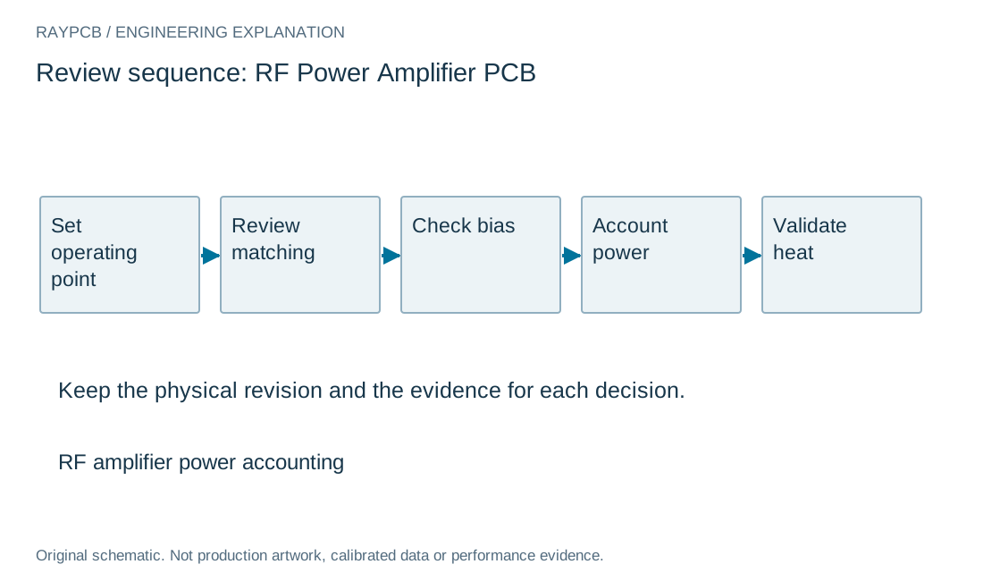
An RF power-amplifier PCB must preserve the active device's electrical and thermal operating conditions. Matching, bias, return paths, supply behavior and heat removal belong to the same integration task. A board built from the right component list can still behave differently from the evaluation circuit if these boundaries change.
The power worksheet on this page accounts for entered DC input, RF input and RF output. It reports the unaccounted power and applicable efficiency ratios. It does not predict junction temperature, stability, compression or a safe operating point.
Define the amplifier operating case
Record the exact device, package, frequency range, bias and signal conditions. Distinguish small-signal gain from the intended output-power operating point. A typical value from a catalogue is not automatically a guaranteed assembled-board result under another waveform or temperature.
Define the power convention: average, per-tone or another explicitly stated quantity. Pulsed or modulated operation can make inconsistent averaging especially misleading. Use compatible conditions for DC and RF measurements so the power balance describes one actual operating case.
Keep the load condition visible. A nominal matched-port measurement and operation into an uncertain installed load are different tasks. Use the selected device's requirements to establish the allowed conditions and protection strategy rather than assuming that a matched bench result covers every antenna state.
Preserve matching and transition geometry
Identify the input and output reference planes of the device model and recommended circuit. Include pads, launches, bias connections and reference conductors in the appropriate analysis. Avoid leaving a package-to-board discontinuity between two otherwise reasonable models.
Use the actual stackup and finished geometry. A reference-board width cannot be transferred blindly to another dielectric height or copper construction. State which features are critical and what supplier adjustments require review. Matching depends on the physical implementation, not only the nominal values in the schematic.
Reserve measurement access deliberately. An added test connector or unused pad can alter the path. The RF transmitter guide connects the amplifier output to filters, cables and antennas so the PA is not evaluated as though the rest of the chain were ideal.
| Review item | What to establish |
|---|---|
| Operating point | Waveform, averaging, bias and load conditions match the power data. |
| Geometry | Device ports, pads and matching structures share a model boundary. |
| Heat | Power accounting and installed thermal paths are separately established. |
| Verification | Gain, distortion, stability and assembly evidence are not conflated. |
RF amplifier power accounting
RF amplifier power accounting
Use the current inputs and keep the assumptions
Enter your own values or use Load example to explore the clearly labeled teaching inputs. The example is not a measured RAYPCB project. Clear for my inputs starts a separate record. Fields identify the units and the physical boundary; missing or unsupported values need correction before a result is generated.
Changing an input invalidates the previous output and disables its download until you generate a new result. A worksheet cannot inspect a board, validate an instrument setup or approve manufacture. Keep its assumptions with any copied number.
Download the current text result if it helps explain a design question. The file stays on your device. Attach or paste it manually when contacting the team; no project information is automatically transferred to the Contact form. Completing this tool is optional.
| Input | What to establish before using it |
|---|---|
| Review reference | Nonconfidential scope or revision. |
| DC input · W | Average input at the declared operating point. |
| RF input · W | Same time and waveform basis. |
| RF output · W | Same system boundary; no missing power sources. |
Follow device-specific bias and sequencing requirements
Obtain the required supply, bias, enable and sequencing instructions for the exact component. Keep them in the bring-up plan and provide practical observation points. Do not infer a safe sequence from an unrelated amplifier family or an apparently similar supply voltage.
Review mounted decoupling and bias networks over the relevant frequency and transient conditions. Pads, vias and return paths are part of those networks. A large nominal capacitor does not automatically provide low impedance at every frequency or prevent every form of instability.
Record control states and software settings with the RF data. Changes in gain mode, bias or enable timing can alter behavior without a board revision. The manufacturing and test instructions should reproduce the accepted operating state rather than relying on a lab engineer's memory.
Use the power-accounting result correctly
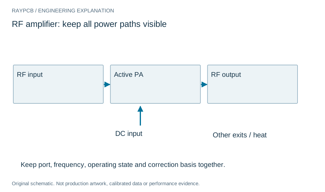
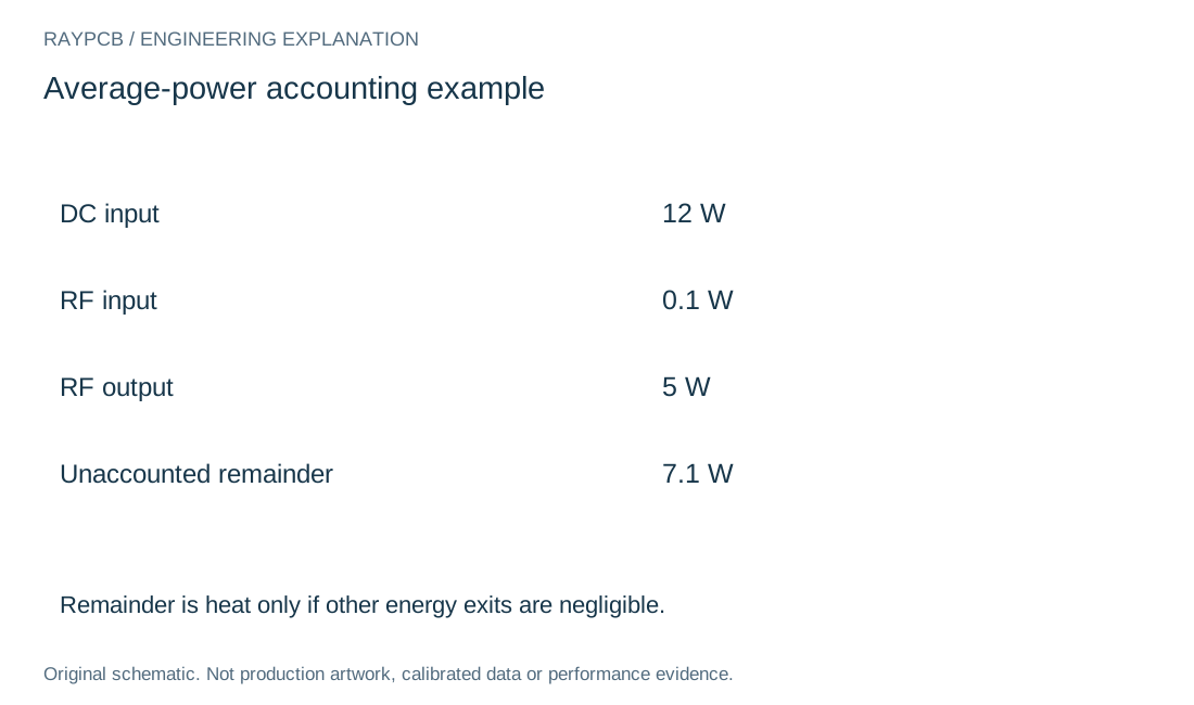
The worksheet calculates DC input plus RF input minus RF output at the declared boundary. This remainder can be a useful heat estimate only when other energy exits are negligible. If power leaves through another RF port or another mechanism, the remainder should not all be labeled device heat.
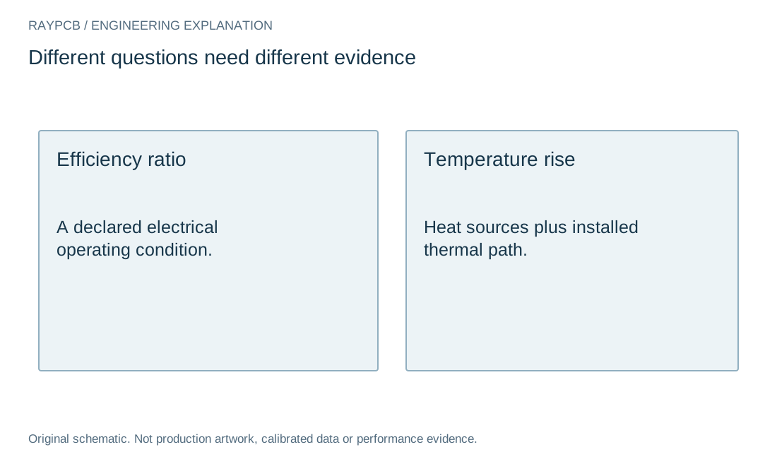
Drain efficiency uses RF output divided by DC input; power-added efficiency subtracts RF input from RF output before dividing by DC input. Both ratios need the relevant measured or modeled values under compatible conditions. The tool withholds those ratios when DC input is zero and preserves a negative PAE when entered values produce one.
As an illustrative case, 12 watts of DC input, 0.1 watt of RF input and 5 watts of RF output leave 7.1 watts unaccounted for. This is an energy calculation, not a RAYPCB module specification or thermal qualification. Analog Devices' PAE definition provides the ratio convention; the physical boundary still belongs to the project.
Build the actual heat path into the design
Identify the device's heat-transfer interfaces and the intended path through the board, mechanical structure and cooling arrangement. Thermal pads, vias, solder interfaces and enclosure contacts may all matter. Specify their construction rather than assuming copper area alone describes the thermal solution.
Use thermal parameters in the conditions for which they are valid. A value obtained on a standard test board or a particular mounting arrangement is not automatically an exact temperature prediction for another product. Include ambient, airflow, interface and duty-cycle assumptions when thermal analysis is required.
Keep distributed RF loss separate from active-device dissipation. The RF laminate heating page explains why lower dielectric loss and higher thermal conductivity are different properties. A material change should address an identified limitation rather than substitute one favorable property for a complete heat-flow review.
Verify gain, linearity and stability with suitable tests
Define the quantities and operating states the amplifier must meet. Gain, return loss, compression, distortion and stability answer different questions. No single clean spectrum or output-power number establishes all of them.
For two-tone distortion, use the IMD3 procedure to separate source and analyzer residuals from the DUT result. Preserve the level sweep, reference planes and correction basis. An extrapolated intercept point is not an allowable output-power specification.
Retain unfavorable conditions and signs of drift. A warmed-up output stage may differ from its initial state, and a temporary bench load may not represent the installed product. Compare results against the agreed operating envelope rather than choosing one favorable point after the fact.
Release the board with assembly and test controls
Coordinate RF geometry with paste, reflow, inspection and thermal-interface requirements. Hidden joints or interfaces can need a defined verification approach. A visually acceptable assembly does not automatically prove that its thermal or RF behavior matches the model.
The enquiry package should include the current board and schematic revision, stackup, exact BOM, operating requirements, quantity and requested assembly or test scope. Mark open questions and proposed alternatives. Manufacturing review and quotation are separate from approval of the complete amplifier design.
The worksheet output can be downloaded locally and attached manually when it explains the power boundary. Completing it is optional. Contact RAYPCB directly for review of the actual files; no entered calculation is automatically treated as a verified performance or capability claim.
Keep efficiency and temperature in separate records
Efficiency ratios summarize a declared power condition. Temperature depends on where the losses occur and how heat leaves the installed structure. Preserve the power boundary and thermal boundary separately so one result does not acquire an unsupported meaning.
When comparing an alternative board or device, hold the waveform and operating point consistent where possible. If the bias or output condition changes, report that change explicitly rather than attributing the entire efficiency or temperature difference to the laminate.
Standards, source context and limits
Use the current document for the exact selected component, construction and test method. A vendor application note is not a universal fabrication rule. Agree any applicable acceptance standard and edition for the project; these public references do not certify a board or reproduce licensed acceptance criteria.
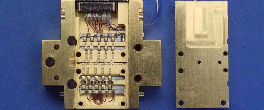
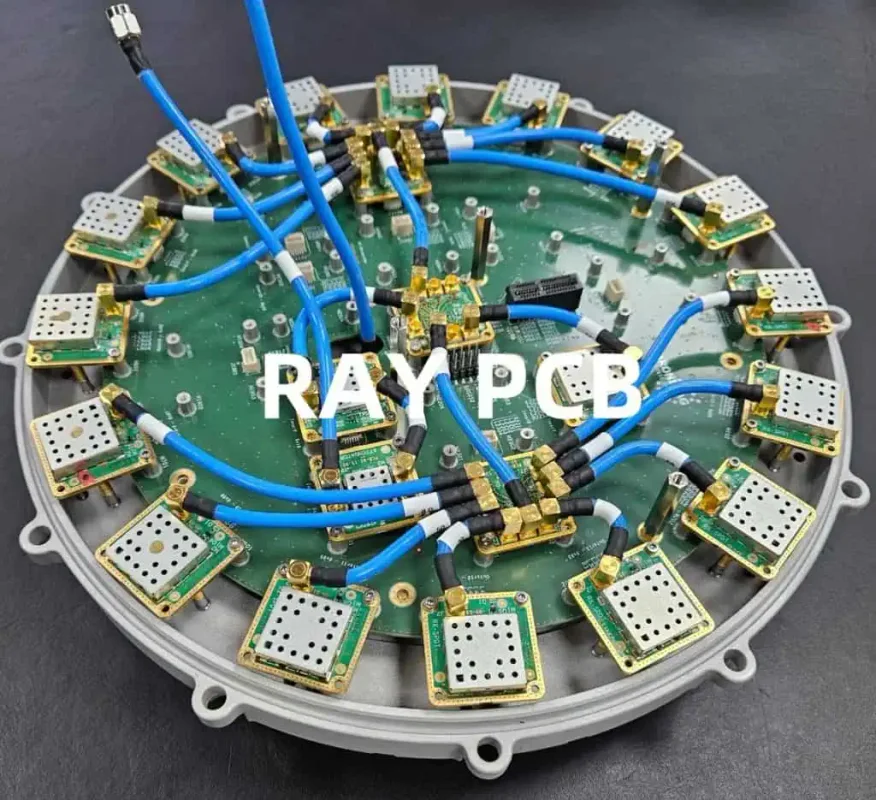
Photographs are identified as existing site archive context. They do not establish current factory ownership, calibrated results or a customer's product performance. Original diagrams explain the named engineering boundary and are not production artwork or field-solver output.
For fabrication scope and the agreed construction requirements, see PCB manufacturing.

