Is Tg130 PCB Enough for your Design

tg130 pcb

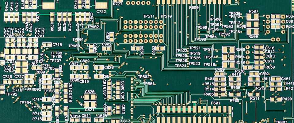
When you first start as an electronics enthusiast, it becomes impossible to imagine how extensive the field can become. Each subject and subject you get to cover in electronics will have more information than the subsequent one. The same applies to printed circuit boards. At first, all that I thought about as an enthusiastic electronic design beginner entailed the need to understand circuit boards, the diverse types in existence, and the manufacture, assembly, and fabrication process. However, ten years and counting, and I still have to learn about specific PCB-related aspects.

This article will detail every crucial detail you have to learn concerning the standard or low tg130 board thickness. Similar to my previous situation, I am sure that reading this piece will prove enlightening, especially in tg130 PCB and other related standard-size printed circuit boards. Let us now get right into it, shall we?

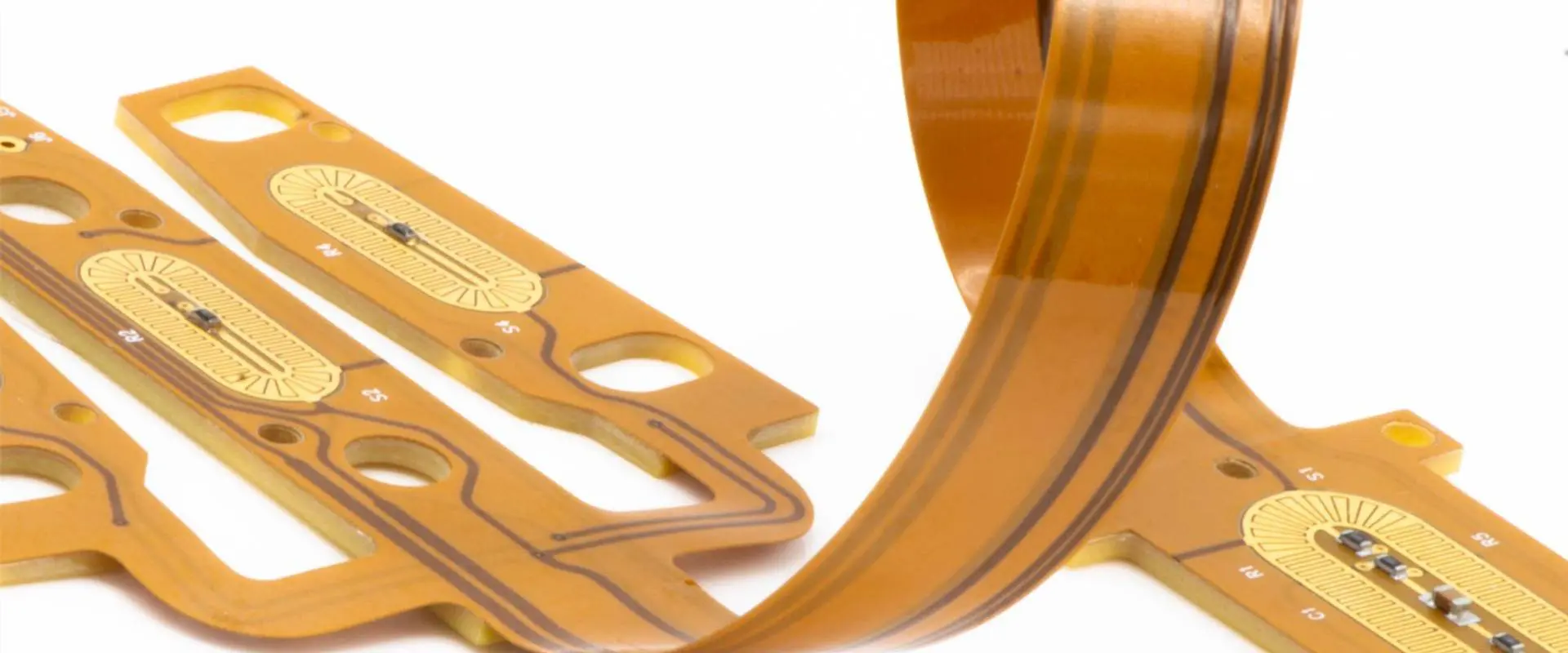
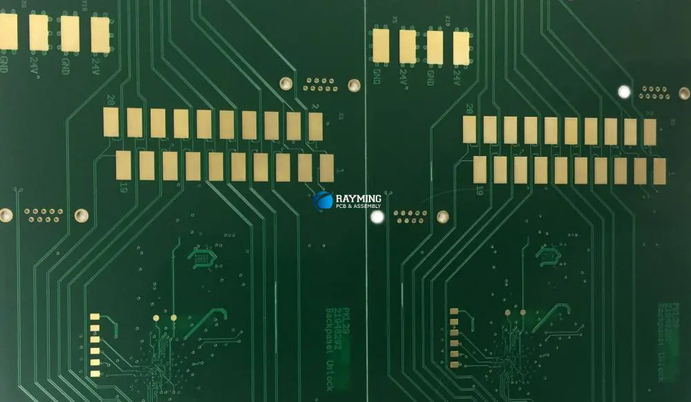
TG130 Printed Circuit Boards

Panasonic R-8700 PCB

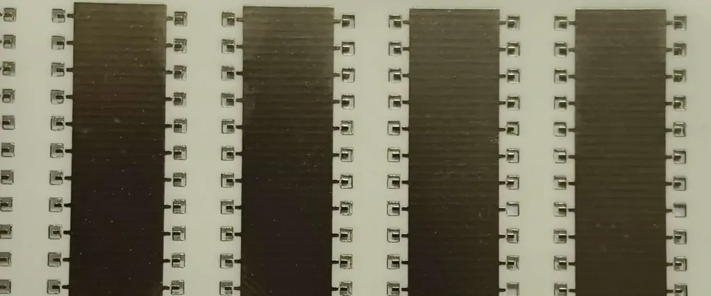
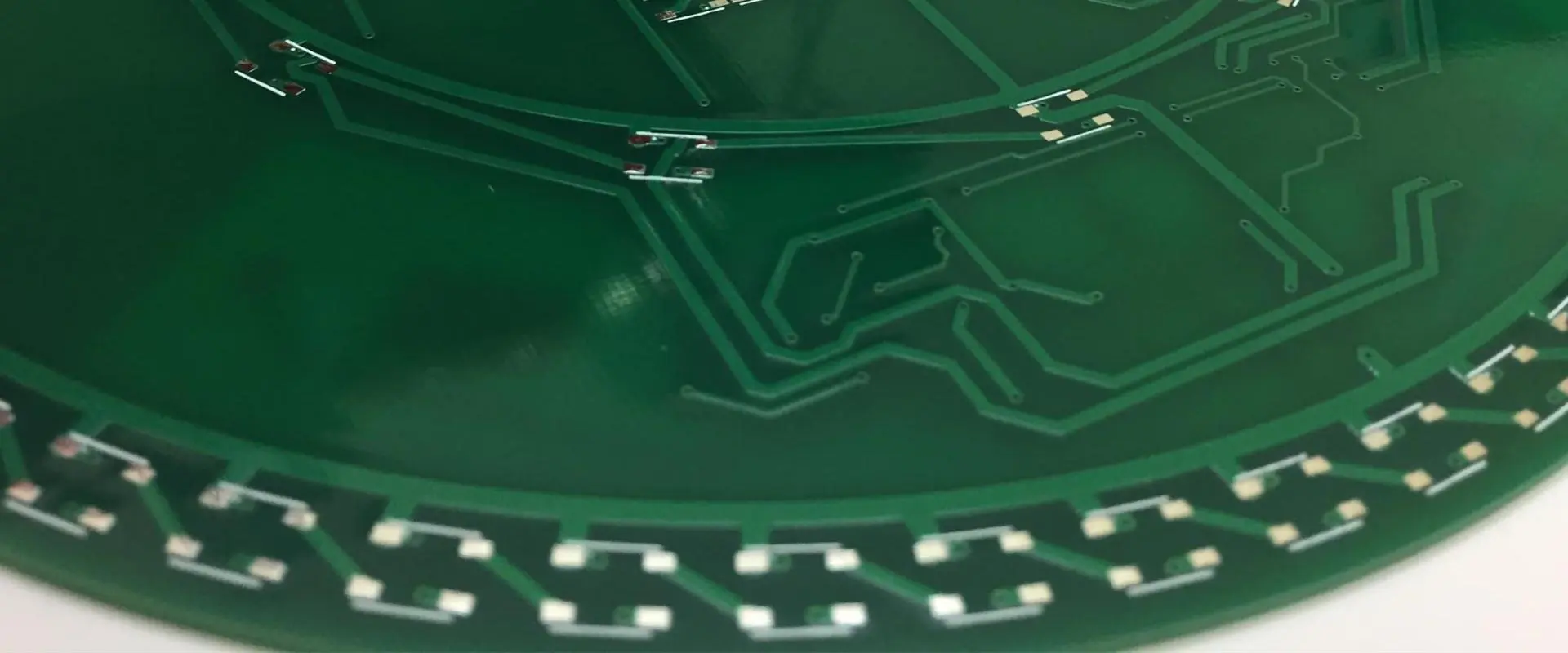
TG often refers to the glass transition temperature, which every printed circuit board possesses to varying degrees. For instance, a standard fr4 tg130 board possess a glass transition temperature value of 130 degree Celsius. The abbreviation term โ€œTGโ€ gets defined as the temperature range upon which the base material of a circuit board becomes unstable (mechanically).

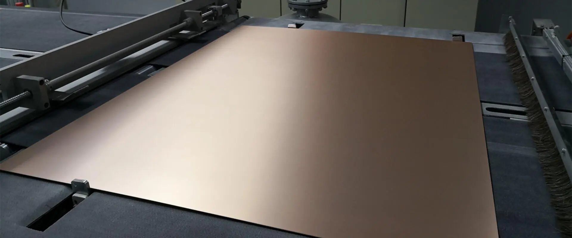
Therefore, a glass transition temperature (Tg) becomes the value of temperature that ascertains a printed circuit board’s mechanical stability, especially in its operational shelf-life. Circuit boards often entail paper or glasslike substances reinforced by resin epoxy to give it its non-conductive and structural platform. In most cases, such material gets referred to as an fr4. A PCB’s fr4 always proves fire-retardant, implying that it cannot get melted or burned by flames or high temperatures. However, this material often changes its form into an amorphous and rubbery state when subjected to higher than conditioned temperatures or Tg values.

An rf4 tg130 board will consist of numerous glass fiber epoxy laminate layers and have a Tg-value of 130 degrees Celsius. While most manufacturers consider the tg130 as the basic low-Tg standard for printed circuit boards, you can always find PCBs with higher TGs falling under the mid-Tg range above 130 degrees Celsius and below the 170 degree Celsius mark. Additionally, there exists the high-glass transition temperature range that starts from 170 degrees Celsius or higher.

Different glass transition temperature value PCBs have different applications with higher TGs proving more suitable to higher operating or manufacturing temperature conditions. However, please note that the TG value should not imply the actual operating temperature of the board. It would help if you always aimed to operate the printed circuit board at about 25 degrees Celsius less of the TG value.

So do you want to procure a standard tg130ย printed circuit board but have no idea what to consider or how to go about it? It would help if you considered the details provided below.

Crucial Information on the Standard TG130 PCB

  • Laminate requirements. It often depends on the thickness of the PCB board desired. The tg130 PCB can come with a board thickness of less than 0.5mm or equal to or above 0.5mm. You have an option of choosing what board thickness you want based on other influencing factors and the purpose of the tg130 printed circuit board.
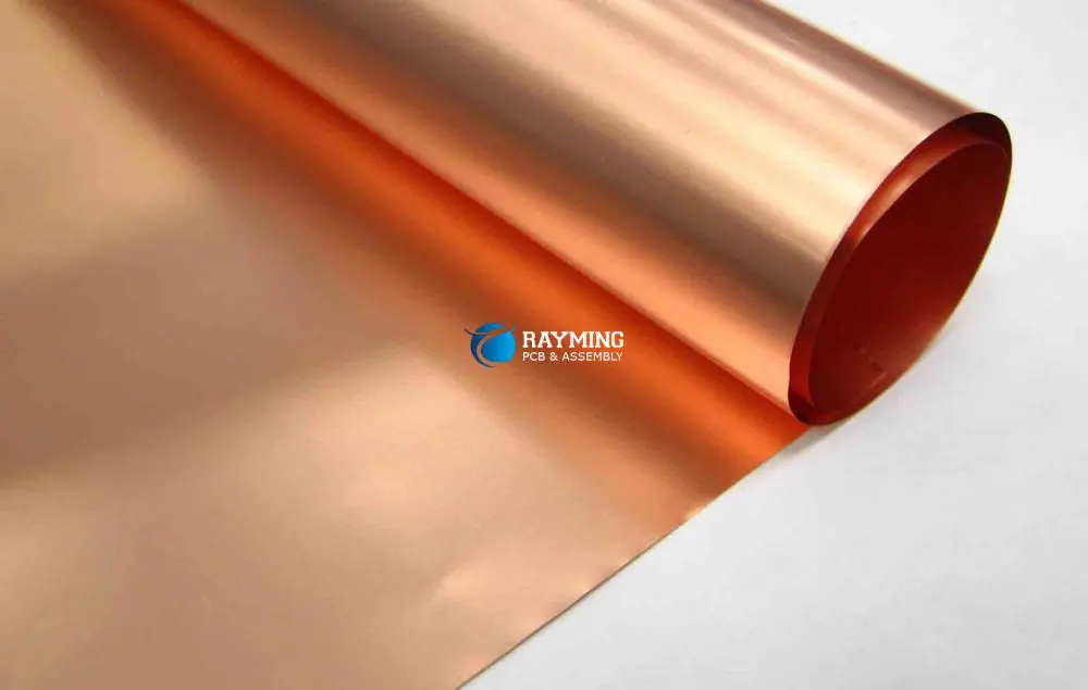
  • Minimum peel strength. The classification includes three broad categories: the standard profile copper foil, the low profile copper foil, and every other foil composite. All three classes possess different values and specifications based on the thickness range. Additionally, the low-profile copper foil can have different values based on the temperature state. For instance, at 125 degrees Celsius, after the process solution, and after the thermal stress.
  • Minimum volume resistivity. Segmented into three categories, the standard tg130 PCB can prove C-96/35/90, post humidity conditioning, and higher temperature E-24/125. All category values and specifications depend on the thickness of the board.
  • Minimum surface resistivity. Three categories of the tg130 PCB exist. It includes the C-96/35/90, post humidity conditioning, and at higher temperature E-24/125. The diverse classes or categories all show diversity concerning board thickness.
  • Maximum moisture absorption with different typical values based on the thickness differences
  • Permittivity and the minimum arc resistance also apply though they differ with the board thickness.
  • Minimum flexural strength comes under two groups of cross and length directions, and these also differ in value and specification depending on the thickness of the tg130 board, especially on the more than 0.5mm thickness.
  • Minimum thermal stress can either as etched or un-etched, with all the tg130 board thickness values passing.
  • Minimum electric strength also differs with the thickness of the board sizes, with thicker board sizes having less strength compared to thinner tg130 PCBs.

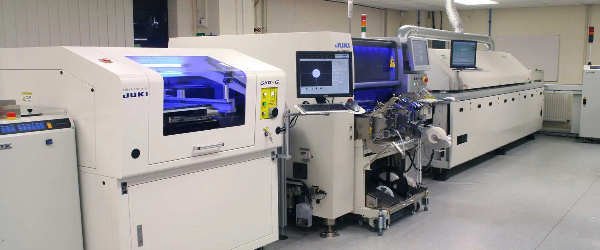
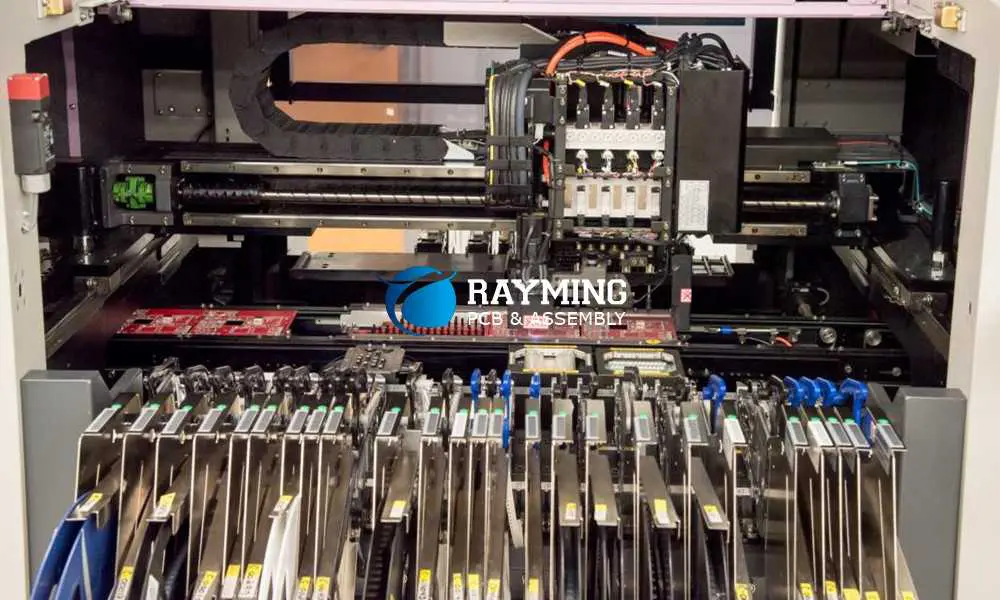
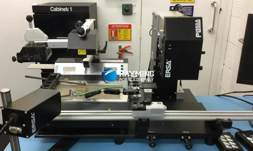
However, if you find these specifications, among others, difficult to understand or unclear, you can always contact your contractual manufacturer for more insights. Here at RayMing PCB and Assembly Company, we provide quality and timely tg130 printed circuit board services. You will benefit from getting quality advice on different aspects of the standard tg130 PCB and benefit from the allied PCB components like the fr4 tb130 and any other fr4 material of your choice. Additionally, you can also enjoy our expert manufacturing, assembly, and fabrication services to ensure an excellent tb130 PCB that fits your design specifications. Therefore, do not waste time and contact us through the stipulated channels on our official website’s home page.

Factors that Influence the Price of a Tg130 PCB

FULL PCB MANUFACTURING Quote

Printed circuit boards, in general, have attributes that can increase or decrease the cost of the PCB. The tg130 PCB proves similar, and its price will get influenced by the following. However, before we get to the price determinants, it becomes essential to note that a tg130 comes as the standard board type. The pricing will prove more affordable compared to higher TG printed circuit boards.  

  • Choice of material. The type of material used will always impact the total cost of a printed circuit board. Materials involved in a tg130 PCB entail the glass-resin epoxy material, the copper layer, and other crucial components. However, the substrate (composed of the fr4) proves the most significant price determinant. The tg130 contains this rf4 material, which costs less than other higher glass transition temperature lamination substrates (like the rf4 tg150, rf4 tg170, etc.). A case in point is the tg150 which costs 5% higher than a tg130 PCB.

Please note that a PCB requiring higher frequencies or speed will need a higher and better grade than the typical fr4 substrate. You may need to use a polyimide material that increases the price by about three times in such a case.

  • The tg130 printed circuit board size will also determine the price directly. It arises because more space implies the need for more materials and more work, which inflates the price. You, therefore, have to consider this aspect when designing your tg130 PCB.
  • Utilization of the working panel. Your PCB will cost less if, in your tg130 design, you have ensured maximum working panel utilization. The percentage of work panel utilization comes as a factor of an array or single unit area and the total quantity within the working layer/panel, all divided by the working panel area, with the result multiplied by one hundred. Therefore, learn to utilize the panel space better to keep your PCB manufacturing costs lower.
  • Via design
  • The design of via deployed in your tg130 PCB will determine the manufacturing cost and thus the price. For instance, when you decide to opt for a via-in-pad design, it will need the plugging of via with resin first before the copper plating process, which will drive up the manufacturing costs. It arises because the drill type for this via design will differ from one via design to the other. For instance, a 0.15mm drill bit can prove expensive besides having the knack of getting broken easily. You, therefore, cannot use this drill type for drilling vias in thicker circuit boards. You, therefore, have to consider this before selecting a manufacturing company and accompanying cost implications in the final PCB prize.
  • The design of the high-density holes will also impact the cost of manufacturing, as it will require more precision and work compared to less-dense holes in the printed circuit board.
  • Tight tolerance. It also influences the price of a standard PCB, especially when excessively tight. Hole sizes need to have a +/- 0.05mm tolerance, with a tighter impedance above +/-10%. Consequently, this provides an aspect ratio of 8:1. It should also possess aย gap and track of less than 4mil/4mil, with tighter outline dimensions of +/- 0.10mm.
  • Lead time. The price of tg130 PCB will depend a lot on the lead time specified. For instance, when you do not provide a timeline for the manufacturer to deliver your PCB, they can work faster, which comes relatively affordable. However, with strict and short timelines, the cost of the PCB will become steeper. The price increase gets accounted for by the contracted manufacturer putting everything else on hold to work on your printed circuit board and deliver within the timelines provided. Consequently, it leads to compensates for the lost opportunity to make money from other similar projects during your work.

Conclusion

If you want to buy a standard tb130 PCB, then without a doubt, we represent the best manufacturing, fabrication, and assembly option for you. Therefore, do not look beyond us, and get to join the more than six thousand contracted customers, happy with our quality PCB products and services.      

Top 10 EMS Electronics Factory in Taiwan

EMS Electronics Factory

Taiwan has established itself as a global electronics manufacturing hub over the past few decades. Many of the world’s top contract manufacturing companies originated in Taiwan and leveraged its robust supply chain ecosystem and engineering talent pool.

In this guide, we will look at the 10 leading EMS (Electronics Manufacturing Services) providers in Taiwan and explore their capabilities, technologies, focus industries and outlook.

Overview of Taiwan’s EMS Industry

Taiwan’s electronics manufacturing industry took off in the 1980s and 1990s as multinationals shifted production to the country. Original equipment manufacturers (OEMs) outsourced manufacturing to lower costs. This gave rise to large contract manufacturers in Taiwan.

Some key facts about electronics manufacturing in Taiwan:

  • Accounts for over 15% of Taiwan’s GDP.
  • Employs over 300,000 skilled workers.
  • Home to over 2,000 electronics companies.
  • Taiwan companies command over 40% global IC foundry marketshare.
  • Major global electronics brands leverage Taiwan’s supply chain ecosystem.

Taiwan provides a robust ecosystem for electronics production comprising component suppliers, raw material providers, PCB/IC substrate fabrication, tooling and a skilled engineering workforce.

Let’s look at the top 10 EMS companies in Taiwan providing end-to-end manufacturing services.

Top 10 EMS Companies in Taiwan

EMS Electronics Manufacturing Companies

1. RayMing Technology

Founded in 2001, RayMing Technology is a professional EMS company providing advanced electronics engineering and manufacturing services including:

  • PCB fabrication, assembly and testing
  • Integrated box build
  • IPD/SiP based miniaturization
  • Process and reliability testing
  • Component sourcing/procurement
  • Product design, prototyping
  • Automation equipment
  • Supply chain and program management

RayMing specializes in high mix, low to medium volume EMS for a range of industries. Their comprehensive capabilities enable concept to mass production product realization.

Manufacturing Capabilities

  • SMT, manual and automated assembly
  • In-circuit, functional, environmental stress test
  • ISO Class 8 cleanrooms
  • Conformal coating, potting
  • X-Ray, AOI optical inspection
  • Centerless grinding, CNC machining
  • Plastic molding and tooling

Facilities

  • Headquarters in Taipei
  • State-of-the-art factory in Taoyuan, Taiwan
  • 3000+ employees across Taiwan and China

2. Pegatron

Pegatron is a leading electronics ODM company headquartered in Taiwan with manufacturing global footprint. They design, prototype and produce electronic devices for global brands.

  • Founded in 2008 as a spin-off of Asus.
  • Employs over 100,000 workers worldwide.
  • Major manufacturing in Taiwan and China.
  • 2021 revenue of approx. $72 billion USD.
  • Services computing, communication and consumer electronics brands.

Pegatron offers vertically integrated production encompassing:

  • Product development, industrial design
  • PCB fabrication
  • Precision enclosures
  • SMT, through hole assembly
  • System integration and testing
  • Support for high mix, flexible volumes
  • After sales repair and services

With expertise across multiple product categories from laptops, smartphones to networking gear, Pegatron has established itself as a marquee ODM servicing top electronics brands.

3. Quanta Computer

Quanta Computer is the largest notebook computer ODM company globally based out of Taiwan. Some facts:

  • Founded in 1988 in Taoyuan, Taiwan.
  • Employs over 90,000 staff worldwide.
  • Operates manufacturing in Taiwan, China, US, Germany, Japan.
  • 2021 revenues of $114 billion.
  • World’s largest manufacturer of laptop PCs.

Quanta leverages its high volume manufacturing expertise and economies of scale to produce notebooks for the world’s leading computer brands along with server systems and data center hardware.

They offer complete services encompassing:

  • Product design, development engineering
  • Component sourcing
  • High volume automated SMT assembly
  • Machined enclosures
  • Final assembly and configuration
  • Worldwide logistics and after-market services

Quanta can rapidly scale production from hundreds of thousands to millions of units annually to meet customer needs.

4. Compal Electronics

Compal Electronics is another major laptop and electronics ODM company based out of Taiwan.

  • Founded in 1984.
  • Employs around 100,000 staff.
  • Operates large campuses in Taiwan and China.
  • Annual revenues of $32 billion.
  • 2nd largest notebook PC maker globally.

Compal utilizes cutting edge Industry 4.0 technologies powered by AI and automation for swift manufacturing. They provide:

  • Notebook, AIO and display product design.
  • Server and storage manufacturing.
  • Quick ramp up to high volume production.
  • IoT and wearable product manufacturing.
  • PCB fabrication and advanced SMT assembly.
  • Aftersales and repair services.

Compal produces at high volumes for the world’s most renowned laptop and electronics brands leveraging efficiency of Taiwan’s supply chain.

5. Inventec

Inventec is a $40 billion revenue ODM company headquartered in Taiwan with a global footprint and 15,000 employees. Their capabilities span:

  • Computing products including notebooks, servers, storage.
  • Networking and telecom equipment manufacturing.
  • Smart devices – phones, wearables, IoT.
  • Automotive electronics and infotainment systems.
  • Appliances, audio equipment.
  • PCBs and components.

Inventec operates advanced manufacturing facilities in Taiwan along with sites in China, Mexico, Czech Republic to provide flexibility in production worldwide.

6. Qisda Corporation

Qisda Corp is a diversified global EMS company based out of Taiwan offering:

  • Contract design and manufacturing for electronics brands.
  • Telecom/networking product manufacturing.
  • Medical and healthcare equipment production.
  • IoT and smart solutions.
  • Robotics, automation and AI technologies.
  • High precision molded plastics.
  • Aftermarket and repair services.

Qisda leverages its engineering expertise across hardware and software to enable IoT based solutions for smart cities, factories, transportation systems and supply chain. Their global footprint across Taiwan, China, Estonia, Germany caters production to both domestic and international customers.

7. Wistron

Wistron is a leading Taiwan headquartered ODM company serving ICT markets with advanced manufacturing.

  • Founded in 2000 after spinoff from Acer.
  • Employs 60,000+ staff globally.
  • 2021 revenues of approx. $27 billion USD.
  • Extensive manufacturing footprint in China along with Taiwan headquarters.

Wistron produces for top electronics brands across:

  • Notebook, desktop, server and datacenter equipment.
  • Networking and telecom infrastructure.
  • Smartphones, tablets, wearables.
  • Medical devices, home appliances, automotive electronics.

From product design through manufacturing to after-sales support, Wistron provides comprehensive contract manufacturing capabilities leveraging their Taiwan supply chain ecosystem.

8. MiTAC

MiTAC is a nearly $4 billion USD revenue ODM company providing complete product realization services:

  • Computing products – laptops, motherboards, servers.
  • Communications infrastructure – networking gear, IoT devices.
  • Industrial automation – panel PCs, PoS devices.
  • Automotive infotainment/telematics systems.
  • PCB fabrication and component distribution.

Based out of Taiwan with operations across Asia, MiTAC caters to verticals like enterprise IT, telecom, IoT, automation and transportation leveraging three decades of ODM experience.

9. Advantech

Founded in 1983, Advantech is a leader in industrial IoT hardware and solutions. While headquartered in Taiwan, they have a global presence.

Key capabilities:

  • Industrial computers – embedded box PCs, panel PCs, motherboards
  • Human machine interfaces (HMI)
  • Industrial IoT edge gateways
  • Automation and control systems
  • Customization services

Advantech works closely with customers right from the design phase through manufacturing, scale up and aftermarket services to provide the optimal industrial automation and control solution tailored to specific needs. Their global footprint enables localized production.

10. Lanner Electronics

Lanner Electronics provides hardware appliances and integrated systems for:

  • Network security – routers, firewalls, uCPEs
  • Critical communications – ruggedized networking
  • Transportation – network video recorders, fleet management
  • Public safety – video surveillance
  • Industrial automation – edge AI solutions

Founded in 1986 and headquartered in Taipei, Lanner possesses advanced design, prototyping and manufacturing capabilities necessary for regulated industries requiring high reliability. Their systems power mission critical applications worldwide across thousands of organizations.

This covers the top 10 EMS providers in Taiwan delivering end-to-end contract manufacturing solutions at various production scales. Taiwan offers a robust ecosystem to manufacture everything from consumer electronics, computers, networking gear, appliances to industrial equipment leveraging skilled engineering talent and supply chain infrastructure.

Electronics Manufacturing Technology Trends

Electronics-Assembly-Companies-in-Turkey

Taiwan’s EMS companies stay at the leading edge by adopting the latest technologies and manufacturing methods. Here are some key trends shaping electronics production –

Smart manufacturing – Artificial intelligence, big data analytics, sensors, IoT and other Industry 4.0 technologies are being deployed across factory floors to gain process visibility, improve quality control and enable flexible volumes.

Advanced automation – Advanced robots, automated material handling systems, software-defined processes controlled via centralized MES systems and precision automation enable optimized high mix production.

Miniaturization – Heterogenous integration technologies like SiP and CoWoS allow integrating of multiple ICs and passives into compact modules or systems-in-package. This supportsminiaturized product designs.

Green manufacturing – With growing environmental regulations and corporate sustainability goals, electronics companies are eliminating waste through material reuse, recycling, energy efficiency innovations and renewable energy usage in facilities.

Digital transformation – Leveraging cloud-based applications, big data analytics and software-defined systems across operations, supply chain and products to increase productivity and agility.

Additive manufacturing – Use of 3D printing for prototyping, tooling and direct part production enables rapid design iteration and part customization.

EMS companies support customers not just through advanced manufacturing but also via product design, simulation, test and software integration services over products’ lifecycles.

Outlook for Taiwan’s EMS Industry

Taiwan’s electronics manufacturing industry appears poised for robust growth through the rest of the decade driven by several key factors.

Geopolitics – Initiatives by governments in US, Europe and Japan are incentivizing localization and reshoring of semiconductor and electronics production capacity. This may accelerate demand for Taiwan’s EMS ecosystem.

Digitization – Broad adoption of digital technologies and IoT is fueling strong growth in connected devices, edge infrastructure, networking hardware, telecom equipment among other electronics.

Electric vehicles – The surge in EVs globally is exponentially increasing electronics content per vehicle providing opportunities for automotive EMS.

Supply chain risks – Companies are seeking alternate sourcing locations to mitigate risks of supply disruptions. Taiwan offers robust ecosystem and proximity benefits for electronics brands.

Sustainability – As stakeholders demand greater supply chain visibility and carbon footprint reduction, Taiwan’s EMS industry is proactively adopting green manufacturing principles.

By continuing technology leadership and expanding value-added capabilities, Taiwan’s EMS sector seems well positioned to capitalize on these industry tailwinds.

Conclusion

Home Electronics PCB

Taiwan provides a strong foundation for electronics product development through advanced manufacturing scaled to global demand. The combination of skilled engineers, cluster of component suppliers, interconnected supply chain and continuous technology adoption enables its EMS companies to deliver high value.

As electronics innovation continues to accelerate, partnering with a Taiwan-based EMS provider offers many benefits for OEMs seeking world-class production and supply chain capabilities.

Frequently Asked Questions

What are the focus industries for Taiwan’s EMS companies?

Computing, communications, consumer electronics, automotive, industrial, medical devices are key sectors served by Taiwan EMS providers.

What manufacturing scales do they support?

Taiwan EMS can support prototypes to high volume production of tens of millions of units annually.

What value-added services do they offer?

Robust product design, simulation, test engineering, software integration, supply chain management and aftermarket support.

What are their quality certifications?

Most hold industry certifications like ISO-9001, IATF 16949 for automotive and are compliant wtih regulations.

Do they have manufacturing operations outside Taiwan?

Many Taiwan EMS companies run campuses in China/SE Asia to diversify risk while serving regional/global customers.

How to Pick a Top EMS Electronic Factory

The existence of plenty of electronic manufacturing services companies and their subsequent production plants or factories in Taiwan can make picking a top factory difficult. You need to understand all the aspects that qualify an EMS electronics factory as a top-tier player before you can settle on one. But before you consider these, you have to look at certain baseline aspects to ensure you stay on track in the selection process of a top-tier EMS electronic factory.

The following, some of the crucial background considerations

  • EMS electronic factory rating. The ratings of an EMS electronic factory often consider plenty of aspects such as capacity, facilities, space, technologies deployed, etc. Therefore, an EMS electronic factory ratings act as an excellent indicator of the factoryโ€™s capacity to design, prototype, and manufacture electronic products and PCBs.
  • Review from previous clients. Plenty of existing and past clients always leave reviews regarding their experiences with the contract electronic manufacturing company. Therefore, it acts as an excellent indicator of the capacity and reliability of the EMS factory.
  • Recommendation. Trusted allies like close friends, family members, and peers can act as an excellent and reliable source for EMS electronic factoriesโ€™ insights. Therefore, always consider their counsel when looking for the best EMS electronic factory for your manufacturing needs.

The baseline consideration should act as the foundation for a steeper and extra determination regarding the suitability of EMS electronic factories. Therefore, try and ask yourself the following questions before settling on a top-tier EMS electronic factory.

Questions to Consider in Picking the Best EMS Electronic Factory

FULL PCB MANUFACTURING Quote
  • Are the EMS company finances stable?

The financial health of a potential EMS company proves a critical aspect in determining the companyโ€™s suitability in manufacturing your electronic needs. Because of this, you have to ensure the manufacturerโ€™s financial health proves adequate and will secure your companyโ€™s financial future. Therefore, besides the manufacturerโ€™s technical competency, service orientation, and price competitiveness, the absence of adequate financial health disqualifies it from an ideal EMS factory for your electronic manufacturing needs.

It all arises because excellent EMS providers need sufficient cash to buy components in advance, as you will always pay them later. Therefore, it falls under the scope of the EMS to cater to all the production costs before getting compensated from your pay, which becomes a possibility with the manufacturerโ€™s healthy financial status.

  • How transparent and open is communication?

The manufacturing process of electronic products often proves complex. It, therefore, requires sufficient and reliable information between both parties to ensure a seamless and quality manufacturing process. All these aspects become possible through proper and honest explanation of the companyโ€™s structure, ability to allow visits during the manufacturing process, etc. Openness and honest communication become fundamental in the proper functioning of a relationship. Therefore the contract manufacturer needs to feel more of a partner rather than the supplier.

  • What certifications types does the manufacturer possess?

A top contract manufacturer needs to have the relevant certifications necessary to develop and manufacture the electronic product. Every industry has particularly required certifications like the ISO13485 and ISO9001 of quality management besides the RoHS compliance. Therefore, it becomes prudent always to discuss such certification requirements ahead of contracting the manufacturer to ensure compliance in completing your electronic production process.

  • How does the EMS Company manage information?

The manufacturing process of electronic products often needs quick and accurate management of extensive data. It arises because components constantly undergo revisions besides EOL. Additionally, delivery dates often change regularly, especially when it comes to sub-suppliers. Therefore, the EMS provider will have to determine that they have got the production underway with the correct component revisions of the earlier specified component. Consider aspects such as the management of engineering changes in the event of new product revisions. The production diary is based on the component delivery dates changingโ€”the absence of a sturdy ERP system by the EMS provider. The voluminous nature of such data and information can prove complex to organize. Therefore, it becomes essential to pick an EMS provider with a defined system of controlling and managing such information internally besides sharing it with you.

  • Is the EMS equipment updated?

Electronics get prone to rapid changes due to constant improvements. Therefore, components keep getting smaller, and this allows for closer PCB placement. Additionally, complex multilayer boards have become the norm, with IoT and wireless components becoming prevalent. You have to determine if the EMS Company has adapted to the tech changes and whether the deployed tools and technologies will suit your modern-oriented electronic product.

  • What type of customer base exists?

It becomes vital to consider the position of the EMS providerโ€™s present customer base besides its size. Consider if the manufacturer can handle the electronic productโ€™s requirements, especially when significant volumes get involved. For instance, if you have low production demands, you can get considerable service and attention. You have to ensure that the contract manufacturer can balance between proving sufficiently sophisticated and staying motivated.

What is Kapton PCB ?

Kapton PCB

What is Kapton

It is a general definition that Kapton is a polyimide. Now for a better understanding of Kapton, you need to understand what is polyimide? When dianhydride and diamine monomers react under condensed conditions, then polyamide is formed. A covalent bond of nitrogen is present with two carbonyl groups in polyimide. The two bonds of the nitrogen and carbonyl group are known as the imine group. Polyimide plays a vital role in a wide variety of application due to high rate of strength and stiffness, high range of operating temperature and inert chemical behavior.

Nowadays, whenever engineers are dealing with harsh applications with a high range of temperature and extreme rate of strength and stiffness, polyamides are preferred to be used there. Several electronic devices, LCDs, gas separations, weapon industries, aerospace industry, and high-temperature polymers are using polyamides.

DuPont in 1960 developed Kapton and the specification of Kapton is it remains stable or in isolation under wide ranges of temperature. Thatโ€™s the reason it has been used in many devices and printed circuits mainly.

Kapton is a highly conductive polyimide, thatโ€™s why it is widely used in electronic devices. The main purpose of using Kapton is to control the heat in electric devices such as Kapton can be a good choice if we need a thin, lightweight, and uniform heater. This lightweight, uniformed nigh temperature performance is required by automotive interior heating, wind turbine, and temperature regulation in aerospace. So polyimide conductive film of Kapton can benefit all of them.

Characteristics of Kapton:

fpc-flexible-printed-circuit

Kapton can be used on extremely high and low-temperature ranges. Kapton can maintain extraordinary mechanical, electrical, and physical properties in the wide range of -452 to 752 Fahrenheit. Kapton is a good resister and an effective insulator so it is a good choice for demanding application industries such as electric applications and aerospace. Below is mentioned some useful features if Kapton:

  • It is highly effective
  • It is highly stable in high ranges of temperatures
  • It can tolerate extreme levels of both heat and cold
  • It possesses excellent mechanical, physical, and electric properties which make it an excellent choice for demanding industries
  • It is well suited for diverse applications
  • It has excellent radiation and chemical resistance
  • It provides reliable labeling

What is Kapton PCB?

Printed circuit boards (PCBs) are the ones in which conductive pathways like tracks and traces laminated with copper are used to support and connect electronic components mechanically. So basically printed circuits boards are designed to support pathways in electronic devices. Every single electronic device consists of printed circuit boards because this is the way of transferring signals within an electronic device.

Once you have understood simple printed circuits, then there comes flexible printed circuit boards. You can make your requirements of interface and depend upon your requirement the flexible printed circuit can be made using polyamide such as Kapton as a base material. A flexible printed circuit board is the further type that is made by using a thin layer of the polymer film (i.e. Kapton) with a conductive pattern of traces on the substrate. So we can say that Kapton is responsible for the flexibility of the printed circuit boards.

Flexible circuits were introduced many years ago, somewhere after the Second World War and the industry is still determined to grow these circuits more potentially. Electric devices often face the harshest temperatures that can go beyond levels. The device may be destroyed if the right material has not been used in it. For overcoming this issue, a polyimide should be used that can withstand increasing temperature conditions. Since 1960, Kapton is the best choice for this problem.   

The main reason for using Kapton in electric devices is heat exposure. As we already know that heat exposure so a common risk in manufacturing electric devices and printed circuit boards also. Temperature can go beyond 400 Fahrenheit. So Kapton is a flame retardant and can expose heat up to 700 Fahrenheit not affect the appearance and performance of the label. Kapton is a highly versatile polyimide material and can withstand severe conditions to offer effective circuit board labeling every time.  

Flexible PCBs can vary from single layer to double layer. But the base layer of polyimide Kapton will be present in every type of printed circuit board.

Single-sided Printed Circuit Board:

Single-sided flexible circuits are the most common and basic flex circuits available in the market. There is a single layer of metal traces on one side of the dielectric. The base layer consists of Kapton polyimide, copper foil, and adhesive supporter. While on the other side like a typical printed circuit board, there is a solder mask sheet and area of connection.

Double-sided Printed Circuit Board:

There are multiple layers on both sides of a single dielectric circuit. There are metalized holes between two layers for plating purposes. On both sides of single dielectric, there are multiple layers for connection, overly, polyimide Kapton and other essentials.

Multi-layer Printed Circuit Board:

There are several layers of copper separated by dielectric layers. These metal layers are then connected by plated holes for making interconnections. Multilayer printed circuit boards are more complex and have complex layers of surface mounting.

Rigid Printed Circuit Boards:

In rigid-flex circuits, the epoxy film is used for connecting multiple layers of printed circuit boards. The component density is higher in these circuits.

Advantages of using Kapton PCB

FULL PCB MANUFACTURING Quote

Kapton printed circuits are serving in many fields. The flexibility of the Kapton circuit boards is the basic requirement for many electronic devices. Following are the advantages of using Kapton printed circuit boards:

  • Kapton printed boards are designed in such a way that they can meet higher and smaller density mountain designs and can improve flexibility. Kapton helps in decreasing the assembly process and reliability can be increased through it. Miniaturization and signals flowing in electric devices can only be improved by Kapton printed circuit boards.
  • There is a thick polyimide film on the substrate of the circuit including a copper foil. For thin and light circuits or compact and complex devices, the solution is ranging through single base Kapton circuit to multilayer or 3D Kapton printed circuit boards. The additional mechanical stability and strength can be enhanced by reinforcing the base material of the circuit. In this way, the strength of the circuit would also be increased.  
  • As clear from the name, the Kapton circuit is having flexibility so it can be bend, move, and torsion effect also. And the conductivity would not be damaged by this flexibility.
  • Due to flexibility, Kapton circuits provide excellent electric performance. There is a good flow of electric signals due to the low dielectric constant. After heat exposure, components can be cool immediately because of good thermal properties. Moreover, components can operate very well under extreme temperature ranges because of higher glass transitions.
  • The other main advantage of using the Kapton printed circuit board is, you can reduce the size of the circuit boards which is required by many applications. Smaller size and lower weight is demanded by many electronic devices such as laptops, computers, military pieces of equipment, aerospace, PDAs, peripheral devices, digital devices, mobile communications, and many other fields also.

Why we rely on Kapton polyimide in our PCB?

It is a fact that Kapton polyimide printed circuit boards are designed to use on specific occasions so you need to know when you can use them and when you should avoid them. The purpose of designing Kapton polyimide circuits was to improve the stability and felicity of the circuit in the reduced weight and size. So following are some reasons we tend to rely on Kapton printed circuits most rather than regular circuits.

Stability of thermal power:

As we already know that polyimide material has excellent resilience and thermal stability which makes it more reliable than any other material. This excellent factor of polyimide material helps in dealing with temperature exposures of electronic devices. Due to Kapton polyimide, electronic devices can work in high temperatures such as under 260 degrees. Moreover, the high stability of thermal power prevents the devices from damages while working and repairing also.

Higher flexibility:

The other greatest benefit of Kapton polyimide circuit boards is their extreme flexibility and stability at the same time. Due to this property, Kapton printed boards can be moved and bend easily. This is the perfect match of flexibility and rigidity in one printed circuit board which normal boards are lacking.

Highly endurable:

Kapton polyimide has a higher level of resistance against temperature and many other chemicals which makes it high durability. This ability is essential for dealing with extreme physical stress.

Final Thoughts

So as a conclusion, we can say that Kapton printed circuits are providing the following key points:

  • Greatly reduced in size and weight
  • More efficiency
  • High integration of components
  • Better wire connection
  • Moving and bending reliability
  • High density
  • High reliability
  • Miniaturization
  • Overall low cost
  • Good solderability
  • Excellent heat dissipation
  • Increase in repeatability
  • Thermal management
  • Improvement in aesthetics
  • Demands for heavy electric devices

Leading PCB Manufacturers in the USA: Key Players & Defense Industry Suppliers (2025)

US PCB Manufacturers

Introduction

The printed circuit board (PCB) manufacturing industry in the United States plays a crucial role in supporting various sectors, including defense, aerospace, telecommunications, and high-tech electronics. As we look ahead to 2025, it’s essential to understand the landscape of USA PCB manufacturers, particularly those serving the defense industry and specializing in high-frequency PCBs. This article will explore the leading American PCB companies, their specialties, and their contributions to the nation’s technological advancement and security.

The Importance of Domestic PCB Manufacturing in the USA

Before delving into the list of top manufacturers, let’s examine why maintaining a strong domestic PCB manufacturing base is critical for the United States:

  1. National Security: Domestic production ensures a secure supply chain for sensitive defense and aerospace applications.
  2. Technological Leadership: PCB manufacturing drives innovation in electronics and advanced materials.
  3. Economic Impact: The industry provides high-skilled jobs and contributes to the US economy.
  4. Rapid Prototyping: Proximity to customers allows for quick turnaround on prototypes and small production runs.

Top PCB Manufacturers in the USA for 2025

1. TTM Technologies

TTM Technologies stands as one of the largest and most diversified PCB manufacturers in North America.

Key Features:

  • Specializes in high-mix, low-volume production
  • Serves aerospace, defense, and medical industries
  • Offers advanced PCB technologies, including HDI and flex/rigid-flex

Defense Capabilities:

  • AS9100 and NADCAP certified
  • Produces PCBs for military communications, radar systems, and avionics

2. Sanmina Corporation

Sanmina is a leading integrated manufacturing solutions provider with strong PCB manufacturing capabilities.

Key Features:

  • Vertical integration from PCB fabrication to full system assembly
  • Global presence with multiple US-based facilities
  • Expertise in high-reliability and complex PCBs

Defense Capabilities:

  • ITAR registered and compliant
  • Supports major defense programs and contractors

3. Cirtech Inc.

Cirtech has established itself as a key player in high-reliability PCB manufacturing for critical applications.

Key Features:

  • Focuses on complex, high-layer count PCBs
  • Specializes in quick-turn prototyping and production
  • Advanced capabilities in via-in-pad and buried/blind vias

Defense Capabilities:

  • AS9100D and ISO 9001:2015 certified
  • Extensive experience with military and aerospace specifications

Read more about:

4. Advanced Circuits

Advanced Circuits is known for its fast turnaround times and broad range of PCB services.

Key Features:

  • Offers standard and advanced PCB technologies
  • Provides free PCB design software and tools
  • Strong focus on customer service and support

Defense Capabilities:

  • ITAR registered and compliant
  • Produces PCBs for military communications and control systems

5. Epec Engineered Technologies

Epec is a versatile PCB manufacturer serving various industries, including defense and aerospace.

Key Features:

  • Offers a wide range of PCB types, including metal-core and rigid-flex
  • Provides engineering support and design services
  • Global sourcing capabilities with US-based quality control

Defense Capabilities:

  • AS9100D and ISO 9001:2015 certified
  • Supports defense contractors with custom PCB solutions

6. Printed Circuits, Inc.

Printed Circuits specializes in flex and rigid-flex PCBs for demanding applications.

Key Features:

  • Expertise in multilayer flex and rigid-flex PCBs
  • Offers fine-line and controlled impedance capabilities
  • In-house design and engineering support

Defense Capabilities:

  • ITAR registered and AS9100D certified
  • Produces PCBs for military wearables and portable electronics

7. Benchmark Electronics

Benchmark Electronics provides end-to-end solutions, including PCB manufacturing for critical applications.

Key Features:

  • Vertical integration from design to full product realization
  • Offers both standard and advanced PCB technologies
  • Strong focus on quality and reliability

Defense Capabilities:

  • ITAR registered and AS9100 certified
  • Supports major defense and aerospace programs

8. Calumet Electronics

Calumet Electronics is a 100% American-owned and operated PCB manufacturer specializing in high-reliability boards.

Key Features:

  • Focuses on high-layer count and complex PCBs
  • Offers quick-turn prototyping and volume production
  • Strong emphasis on research and development

Defense Capabilities:

  • ITAR registered and AS9100D certified
  • Produces PCBs for mission-critical defense applications

9. Sierra Circuits

Sierra Circuits is known for its advanced PCB manufacturing capabilities and quick turnaround times.

Key Features:

  • Specializes in HDI and high-frequency PCBs
  • Offers comprehensive DFM (Design for Manufacturing) support
  • Provides online instant quotes and ordering

Defense Capabilities:

  • ITAR registered and AS9100D certified
  • Supports defense contractors with high-performance PCB solutions

10. Marino Manufacturing

Marino Manufacturing has built a strong reputation in the defense and aerospace PCB market.

Key Features:

  • Specializes in complex, high-reliability PCBs
  • Offers both prototype and production services
  • Provides comprehensive testing and quality assurance

Defense Capabilities:

  • ITAR registered and AS9100D certified
  • Extensive experience with military specifications and standards

High-Frequency PCB Manufacturers in the USA

Rogers RT duroid 6006 PCB

High-frequency PCBs are critical components in many defense and telecommunications applications. Here are some leading USA PCB manufacturers specializing in high-frequency PCBs:

1. TTM Technologies

TTM has significant expertise in high-frequency PCB design and manufacturing.

Key Capabilities:

  • Production of PCBs for 5G infrastructure
  • Specializes in RF and microwave PCBs
  • Offers advanced materials for high-frequency applications

2. Compunetics, Inc.

Compunetics is a leader in high-frequency and high-speed PCB manufacturing.

Key Capabilities:

  • Expertise in controlled impedance and low-loss designs
  • Offers a wide range of high-frequency PCB materials
  • Provides engineering support for complex RF designs

3. Multilayer Prototypes, Inc.

Multilayer Prototypes specializes in quick-turn, complex PCBs, including high-frequency boards.

Key Capabilities:

  • Offers PCBs for frequencies up to 77 GHz
  • Provides advanced via structures for high-frequency applications
  • Expertise in hybrid constructions using multiple materials

Factors Driving the Growth of PCB Manufacturing in the USA

Several factors contribute to the continued growth and importance of PCB manufacturing in the United States:

1. Reshoring Initiatives

There’s a growing trend of bringing manufacturing back to the USA, driven by:

  • Concerns over supply chain security
  • Desire for better quality control
  • Need for faster turnaround times

2. Technological Advancements

USA PCB manufacturers are investing in cutting-edge technologies:

  • Advanced materials for high-frequency and high-speed applications
  • Additive manufacturing processes for PCB production
  • Increased automation and Industry 4.0 integration

3. Defense Spending

Continued investment in defense and aerospace drives demand for high-reliability PCBs:

  • Modernization of military communication systems
  • Development of advanced radar and electronic warfare systems
  • Increased focus on cybersecurity hardware

4. 5G and Telecommunications

The rollout of 5G networks creates demand for high-frequency PCBs:

  • Infrastructure equipment requiring specialized PCBs
  • IoT devices with integrated high-frequency capabilities
  • Advancement in satellite communication systems

Challenges Facing USA PCB Manufacturers

Despite the growth opportunities, PCB manufacturers in the USA face several challenges:

1. Global Competition

USA PCB manufacturers must compete with lower-cost producers from Asia and other regions.

2. Skilled Labor Shortage

The industry faces a shortage of skilled workers, particularly in advanced PCB technologies.

3. Raw Material Costs

Fluctuations in raw material prices can impact profitability and competitiveness.

4. Regulatory Compliance

Stringent environmental and safety regulations add complexity and cost to PCB manufacturing processes.

Future Outlook for PCB Manufacturing in the USA

The future of PCB manufacturing in the United States looks promising, with several trends shaping the industry:

1. Increased Focus on Advanced Technologies

USA PCB manufacturers are likely to invest more in advanced technologies such as:

2. Emphasis on Sustainable Manufacturing

There will be a growing focus on developing eco-friendly PCB manufacturing processes and materials.

3. Automation and AI Integration

Increased use of automation and artificial intelligence in PCB design and manufacturing processes.

4. Specialization in High-Value Markets

USA PCB manufacturers are expected to focus more on high-value, complex PCBs for specialized applications.

Conclusion

The PCB manufacturing industry in the United States continues to play a crucial role in supporting critical sectors such as defense, aerospace, and high-tech electronics. The top manufacturers listed above are at the forefront of innovation, driving advancements in PCB technology and maintaining the nation’s technological edge.

For businesses and organizations seeking high-quality, reliable PCBs, especially for defense applications or high-frequency needs, these USA PCB manufacturers offer a range of solutions backed by extensive experience and advanced capabilities. As the industry evolves to meet new challenges and opportunities, American PCB companies are well-positioned to maintain their leadership in producing cutting-edge, high-reliability printed circuit boards.

FAQs

Q1: Why choose a USA-based PCB manufacturer for defense applications?

USA-based PCB manufacturers offer several advantages for defense applications, including ITAR compliance, secure supply chains, and extensive experience with military specifications.

Q2: What certifications should I look for in a PCB manufacturer for aerospace applications?

Key certifications for aerospace PCB manufacturers include AS9100, NADCAP, and ISO 9001:2015.

Q3: How do USA PCB manufacturers compete with lower-cost overseas producers?

USA PCB manufacturers compete by focusing on high-quality, complex PCBs, offering quick turnaround times, and providing extensive engineering support and customer service.

Q4: What are the advantages of working with a PCB manufacturer that offers both prototyping and production services?

Working with a PCB manufacturer that offers both prototyping and production services ensures consistency throughout the development process, reduces time-to-market, and often results in better design for manufacturability.

Q5: How are USA PCB manufacturers addressing environmental concerns?

Many USA PCB manufacturers are adopting eco-friendly practices, investing in more efficient equipment, and exploring alternative materials to reduce their environmental impact while meeting stringent quality standards.

Top 10 SMT Assembly Brand Machines

SMT Machine

Smart Factory Solution is fast becoming a trend in the electronics manufacturing industry. This is relevant because of the need to cut down on costs, improve the speed of production and do away with some of the challenges that restrict improved efficiency of production.

Surface Mount Technology (SMT) machines play an important role in the provision of responsive manufacturing solutions.

This guide explains the concept of Surface Mount Technology (SMT), the different types or brands of SMT machines, and the companies or brands that manufacture these machines.

What is Surface Mount Technology?

Surface Mount Technology, also called SMT, is a type of electrical component production that involves the mounting of the electrical components directly on the surface of a Printed Circuit Board (PCB).

The relevance of SMT has gone a long way to replace the former electronic component production format โ€“ Through-Hole Technology.

One of the many advantages of manufacturing with Surface Mount Technology (SMT) is that it makes it easier for production to be scaled in real-time. In addition to the speed that comes with it, SMT also helps to cut down on the cost of electronics production because fewer hands are needed.

The electronic devices that are manufactured by using Surface Mount Technology (SMT) are called Surface Mount Devices (SMDs).

What does Surface Mount Machine do?

Surface Mount Machines are also called Pick-and-place machines or SMT Component Placement Systems.

These machines are robotic machines used for placing Surface Mount Devices (SMDs) onto Printed Circuit Boards (PCBs).

These machines are commonly used because of the high precisions, several use cases/applications, and the variety of electronic components that can be used on them.

Types of SMT Assembly Machines

smd machines

A bulk of the increased success rate of using Surface Mount Technology (SMT) machines depends on the inputs of the different machines used in the process.

We are not talking about one machine. Up to six (6) machines are used to facilitate the placement of electronic components on the circuit boards.

Below are some of the popular pick-and-place machines and the work they do in terms of Surface Mount Technology (SMT).

1. Pick-and-Place Machines

This is the first type of SMT Assembly machine. Pick-and-place machines are used to pick up and place or position the Surface Mount Device (SMD) electronic components onto the Printed Circuit Board (PCB).

The placement is immediately followed by the soldering of those SMD components to make them stick to the circuit board.

Lots of factors are considered before deciding on the model of Pick-and-place machines to buy. These machines are categorized into different types.

These include:

Manual Pick-and-place Machines

These are the most common type of Pick-and-place machines. As the name suggests, the process of picking and placing the Surface Mount Device (SMD) on the PCB is done manually.

Worthy of mention is that manual pick-and-place machines are often used for modular PCB production needs. The manual machines can also be used when there is a need to customize the components for high-speed, unattended operations.

Using the manual pick-and-place machines is an ideal way to derive improved yield, reduce fatigue on the part of the operator, and cut down on placement errors.

Although the accuracy of the placement is not always assured because of the potential limitations faced by the operator.

That notwithstanding, the manual pick-and-place machine does a great job of bolstering the incremental production of hand-held volumes.

Semi-Automatic Pick-and-place Machine

The semi-automatic pick-and-place machines were originally designed to be the interface between the manual and the automatic pick-and-place machines.

These semi-automatic pick-and-place machines did an excellent job of providing a vision-assisted computer interface that makes it easier for the operator to see the direction of the component. This way, the operator will make accurate placement of the ultra-fine pitch components.

The only difference is that the Semi-automatic pick-and-place machine still works with manual placements. So, the operator has to manually position the components for low-volume applications.

Automatic Pick-and-place Machines

Automatic SMT machines replaced the semi-automatic models. The automatic model was improved to make the transition of the leap from manual to fully automated SMT machines.

Among many other things, automatic SMT machines are fully equipped with pick and place centering methods, as well as improved machine capabilities, in the areas of repeatability and accuracy.

2. SMT Curing Oven

This is also called the Surface Mount Technology (SMT) Baking Oven. The SMT Curing Oven is an oven used for the baking of solder paste and adhesive curing.

The volume of production also determines the possibility of combining the trio of solder paste baking, adhesive curing, and solder reflow.

3. Solder Paste Screen Printer

This is the third type of SMT assembly machine. The Solder Paste Screen Printer is a machine used for screen printing the solder paste onto the circuit board (PCB).

This is often done before the Surface Mount Device (SMD) components will be placed atop the Printed Circuit Board (PCB).

4. Reflow Soldering Machine

The Reflow Soldering Machine accounts for about 25% of the total cost of a Surface Mount Technology (SMT) device.

This SMT machine is primarily used for enabling solder reflow from the Surface Mount Device (SMD) to the circuit board. This is done after the reflow soldering is done with solder paste.

5. Solvent Cleaning Equipment

The soldering process is not always neat. There are chances of flux and excess solder remaining after the entire process.

That is why you need to use the Solvent Cleaning Equipment. This SMT Machine is used to clean and remove the excess flux and solder from the Printed Circuit Board (PCB) after soldering.

6. Inspection Equipment

The Repair and Inspection Equipment is another type of Surface Mount Technology (SMT) machine that is required in the SMT assembly process.

The PCB Inspection Equipment is an SMT Machine used for inspecting the Printed Circuit Board (PCB). The inspection is done to inspect the circuit board to check for potential defects.

The machine does not only find out the defects or faults in the circuit board. It is also used to repair or fix those defects.

Soldering Iron and Hot Air SMD Rework Station are two of the most used types of PCB Inspection Equipment that are used for the detection and repair of this defect.

The Best SMT Assembly Machine Manufacturers

FULL PCB MANUFACTURING Quote

We are now going to review some of the best brands and companies that manufacture different kinds of Surface Mount Technology (SMT) machines.

Mycronic is the first SMT assembly manufacturer on the list. This is one of the best SMT assembly manufacturers that focus on the production, distribution, and management of sophisticated pick-and-place machines.

1. Mycronic

The MY300 is the most outstanding of the SMT machines manufactured by Mycronic. With this pick-and-place machine, operators are confident of populating more boards with less floor space.

Features of Mycronic SMT Machine

These are some of the features of the Surface Mount Technology (SMT) manufactured and distributed by Mycronic:

Strong Software Suite

The pick-and-place machine is built with a powerful software suite that is both versatile and user-friendly.

The relevance of this SMT machine software is that it makes it simpler for machine operators, planners, stock managers, and engineers to have access to update information about SMT machine uses.

Precise Material Handling

You do not necessarily need to overwork yourself by working with complex material handling.

Instead, you want to use the precise material handling feature of the Mycronic SMT machine to avoid the bottlenecks that come with the complex handling of SMT materials.

This way, you will leverage the versatile pick-and-place solution offered by Mycronic SMT machines to produce as many circuit boards as you want in a day.

2. JUKI Automation Systems

JUKI is one of the leading manufacturers of Surface Mount Technology (SMT) machines. The company has been in the business for many years. Thus, it is in a better position to offer the desired SMT machine solutions.

Let us go into details of what JUKI has to offer, as far as Surface Mount Technology (SMT) machines are concerned.

The Company Builds a Large Portfolio of Placement Machines

JUKI is reputed for the large portfolio of pick-and-place machines it manufactures. The company manufactures SMT machines for small, mid-sized, and large companies.

Performance

The performance of the SMT machines is not in doubt because JUKI places a premium on the development of high-quality and high-performance pick-and-place machines.

Placement Capabilities

The JUKI SMT machines are also designed in a way that the machines will make accurate placement of the components on top of the Printed Circuit Board (PCB).

3. DDM Novastar

DDM Novastar is one of the leading manufacturers of pick-and-place equipment designed for use in both manual and automated SMT systems.

So far, the company has been able to manufacture about 26,000 SMTs, of which the customers are satisfied with their purchase.

DDM Novastar also designs the pick-and-place equipment to work in low-to-medium SMT machine applications.

This is in addition to the reliability, ease of operation, quick set-up, and affordable costs of the pick-and-place machines.

Below are some of the reasons why engineers and machine operators prefer to use SMT machines manufactured by DDM Novastar:

Different Types of SMT Machines

One of the reasons why SMT machine operators like DDM Novastar is because the company offers a wide range of pick-and-place machines.

These machines include manual types and automated types. For the manual models, we have many designs, such as:

  • MPP-11 Manual Desktop Pick and Place Machine
  • MPP-21 Pick and Place System

The automatic SMT machines manufactured by DDM Novastar include:

  • LE40 Pick and Place Machine
  • The Low-Cost NovaPlace Pick and Place Machine
  • LS60 Pick and Place Machine
  • LS40V Pick and Place Machine with Vision
  • LE-40V Pick and Place Equipment with Vision

Turnkey SMT Assembly Systems

DDM Novastar is also one of the manufacturers of pieces of SMT assembly equipment required for the manufacturing of a complete Printed Circuit Board (PCB) solution.

The company offers its complete SMT assembly systems to be used for high-volume PCB assembly, cost-effective prototyping, and pilot manufacturing.

The DDM Novastar turnkey SMT solutions are also used for manual SMT prototyping, medium volume throughput, automatic prototyping, and low-volume throughput.

Unique Programming Software

DDM Novastar also adds something important to the full-scale SMT assembly services it offers.

The company offers unique programming software. The name of the software is SMTrue Run Optimize Software.

The software is used for making offline programming of automatic SMT machines. This way, it will easier to derive increased efficiency and throughput from the machine.

Different Levels of Automation

Another unique feature of the DDM Novastar pick-and-place machines is the different levels that are used to automate the workings of the machine.

These levels of automation have to do with the different production stages and capabilities of the DDM Novastar SMT machines.

The minimum number of components that can be assembled per hour is 50. That is if you are using the Manual (hand) SMT machine.

It can be as high as 30,000 Components per Hour (CPH) if you are using the Fully Automatic (High-Speed) Free-Standing or Modular SMT machine.

Affordable Pick-and-place Machines

DDM Novastar also manufactures pick-and-place machines that wouldnโ€™t dip a hole in your pocket.

The price of the SMT machines starts from $300-$400 for the Manual (Hand) and can be as high as $100,000 for the fully automatic variant.

4. Yamaha Motor

Yamaha is another company that specializes in the production of Surface Mount Technology (SMT) machines.

The company focuses on the production of pick-and-place machines that will offer the operators smart manufacturing solutions.

So, if you are looking to realize smart manufacturing with pick-and-place machines, Yamaha Motor is the manufacturer you should be talking to.

Here are some of the reasons why Yamaha Motor s one of the best SMT Assembly machine manufacturers:

A Full Lineup of SMT Machines

One of the advantages that set Yamaha Motor many miles ahead of the competition is the wide range of SMT products the manufacturer offers.

This SMT machine lineup ranges from SMD Storage System, Surface Mounter, Inspection System, Management Software, Solder-Paste Printer, Flip Chip Bonder & Hybrid Placer, and Dispenser.

Competitive Pricing

Yamaha Motor also beats the other SMT machine manufacturers to the competition by offering competitive prices.

No matter your budget, rest assured that there is a pick-and-place machine that matches your needs.

5. Europlacer

If there is any SMT machine manufacturer that worth the onion, it has to be Europlacer. The company has consistently shown up over the last couple of years to manufacture, distribute and manage several pick-and-place machines.

These SMT machine services are no unconnected to the dedication of the manufacturer to design and distribute some of the best high-mix pick-and-place Surface Mount Technology (SMT) machines.

This is in addition to the fact that Europlacer manufactures these machines to fit into your business needs. You neednโ€™t forfeit one feature for the other because Europlacer took care to ensure that the SMT machines are designed to adapt to your business needs without any need to sacrifice quality or output.

The SMT machines produced by Europlacer pack many features, including:

  • Automation
  • Smart nozzles
  • High accuracy
  • Fixed camera
  • Upgradeability
  • Electrical testing
  • High speed
  • Service and maintenance

6. Neoden SMT

Neoden SMT is a reliable Surface Mount Technology (SMT) machine manufacturer. The company specializes in the production and management of a full automatic SMT line.

That is not all!

The manufacturer also manufactures a high-speed Printed Circuit Board (PCB) assembly line. This is designed to satisfy any batch of PCB assembly.

The company also manufactures different SMT machines that are designed to give the machine operators multiple options to choose from as far as Surface Mount Technology (SMT) is concerned.

7. Panasonic

Panasonic is one of the advocates for Smart Factory Solutions. They have since followed it up with the production of Surface Mount Technology (SMT) machines that offer best-in-class solutions to the users.

The SMT machines distributed by Panasonic are also versatile. You can get machines for both entry-level and more complex requirements.

In addition, you can use these SMT machines for any volume and any mix of your Smart Manufacturing needs.

8. Hanwha Precision Machinery

Last but not least on our list of Surface Mount Technology (SMT) machine manufacturers is Hanwha Precision Machinery.

The company manufactured the first chip mounter in 1989. Since then, the manufacturer has delved into many other relevant manufacturing processes, including integrated software solutions, semiconductor equipment production, Surface Mount Technology (SMT) mounters, industrial automation equipment, and insertion & equipment automation equipment.

The company also offers excellent customer service that is targeted at delivering more value, greater efficiency, and versatility.

How to Choose the Best SMT Machine

bga-rework-machine

Choosing a pick-and-place machine can be tricky, especially when you donโ€™t know what to look for. That is why you need to learn about some of the important features you must look for in any SMT machine.

These factors worth considering are:

1. Placement Speed

The speed at which the pick-and-place machine works is very important. You want to consider this first before any other thing because it is one of the important features that make the SMT machine work as it should.

Also, you need to understand that the placement speed has to do with the speed or rate at which the SMT machine picks up the SMT components inspects the components before placing the components on the Printed Circuit Board (PCB).

The other important factor you want to consider about the placement speed is the standard rating of IPC 9850. This is the standard used by many SMT manufacturers to rate the speed of the pick-and-place machines. Besides, the IPC 9850 speed or rating standard has to do with the general guidelines for the circuit board arrays and the part mix.

The rule of thumb is for you to devalue any figure that the manufacturer may have given. The devaluation is important because the speed quoted by the manufacturers is usually lowered by 30% or 40%.

Therefore, you will get an accurate value or figure of the potential rate or speed of the SMT machine if you make some divisions. The best way to divide is by devaluing or reducing the placement rate of the machineโ€™s rate by 30%. This way, you will have a clear speed value that the SMT machine can deliver.

2. Accuracy & Repeatability

The other important factor you want to consider is the accuracy and the repeatability of the pick-and-place machine.

This is important, considering that the accuracy of the machine plays an important role in the picking, inspection, and placement of the components on the Printed Circuit Board (PCB).

Worthy of mention is that the quality of the SMT machine is very important when looking for accuracy and repeatability in the pick-and-place machine.

The best SMT machine with the best accuracy is the one that has an accuracy of 0.0001โ€ and a fine pitch lead of 12mil.

This should be done repeatedly for maximum outputs.

We wouldnโ€™t fail to mention that the pick-and-place machine you want to buy should be the one that has programming software, as well as a computer. These two will go a long way to take care of the continued repetition of the component placements.

3. Size of the Parts

Have you taken the time to consider the size of the parts you want to place on the pick-and-place machine?

The size of the parts matters a lot because you need to find a Surface Mount Technology (SMT) machine that matches the size of the parts you want to use to pick, inspect and place on the circuit board.

The general rule is to buy a pick-and-place machine (P&P) that can pick components with the sizes:

  • 0402
  • 0201
  • 01005

If the SMT machine cannot pick those, it means that you may need to make special arrangements. This is common if the size of the SMT components is below or less than 0402.

In that case, you will need to get a nozzle or an additional feeder to streamline the design of such a component.

Wrapping Up

Surface Mount Technology (SMT) machines or pick-and-place machines are very necessary for the production of Printed Circuit Boards (PCBs). These machines make the job of mounting the components on the circuit board faster and easier. And you will save more money and spend less time.

Thus, consider the important factors we just shared in this article so you can find the best SMT assembly machine to buy for your PCB design needs.

Getting to Understand about 3mm PCB

3.0 mm pcb

Are you interested in fr4 3mm PCB but do not know much about it? A 3mm PCB has the same size as a credit card and can fit in your wallet. This makes it such an attractive option for projects that need to be portable and need to be taken on the go. Many people also suggest that this size is perfect for international travel, so you can pack your project away in your backpack or purse and take it with you.

A green PCB material has low conductivity.

A wood-based PCB material has high conductivity.

This article will go over some of the key features of a 3mm PCB and its drawbacks. Also, we’ll go over some popular applications of this size of PCB.

What is 3mm PCB?

The PCB is the printed circuit board, a printed circuit layer assembled with electronics and components in an integrated manner on a flat surface. The simplest way to describe it would be as a printed circuit board with a thickness of only three millimeters. The thickness of a PCB board depends on the type of circuit material used. It can be 1 oz copper or 1-2 oz copper with another metal such as gold for better conductivity along traces on the board’s surface. For special types of circuits such as RF devices and high power battery circuits, other types of substrates may be required, and there are different names for these depending on their construction. The comparison of the surface area to the height makes this type of PCB perfect for smaller items. These boards are mostly used for portable accessories like cell phones, cameras, MP3 players, etc. Despite their relatively small size, they can still accommodate a large amount of circuitry within them.

Types of PCB Board

A well-known type of PCB is FR-4, which stands for flame retardant 4. It is FR-4 that is used for servicing the majority of electronic devices and circuits in the world today. This material is made up of a high-frequency glass fabric that has been impregnated with a thermosetting resin made from epoxy resin. The epoxy resin provides the necessary strength and rigidity for the board and its ability to withstand high temperatures during soldering.

Other types of PCB material include:

FR-1 is a flame retardant laminate with epoxy resin, but it will melt at low temperatures and is not recommended for PCB construction.

3mm thick FR-2 is comprised of an epoxy resin and a fiberglass fabric. This board has high rigidity, but it is not flame retardant and can burn easily with a hot iron.

FR-6 also contains glass fibers, but the resin used on this board is a vinyl ester. It is the same as FR-2 above, but it has a higher melting point. It can be used for very thin boards or double-sided boards.

Various conductive and insulating PCB materials are available: gold, silver, tin, tungsten, iron, copper, gold wire. These can be used for flexibility or high resistance circuits.

What are the advantages of 3mm PCB?

fr4 3mm PCB

3mm PCB is a small size circuit board; its size is smaller than a card. Especially fr4 3mm size is suitable for designing the smart-card application of small electronic components COSPLAY, which can be used in banking and payment cards, such as security devices. The weight of a green sheet is very light; it is easy to carry and use in mobile devices. What’s more, it has no space limitations with large quantities on export.

3mm PCB can be used for more than mobile phones, such as portable games, smartwatches, smart home appliances, and 3C electronic products.

This kind of circuit board is suitable for making small circuit board sizes to save material and reduce the weight and size of the electronic components. The miniaturization effect can bring the component size down by over 90% (compared with a general size of 15 x 15mm).

The circuit board is easy to carry;

There is no limitation for the export of large quantities;

The circuit board can be made into small sizes;

It has a good heat dissipation effect;

It can replace the general size of the electronic components by over 90%;

It is not easy to produce the radiation of electromagnetic interference.

Standardization and Form Factor

A 3mm design is only standardized when the oldest version is created. Since 3mm PCBs are so new, the design standards will change as time goes on and new versions are created. For example, a 3mm board designed for the newest version 1.4 will not fit on a 1.0 board because of the change in size from 1 to 2 inches.

Since there is no general standard for this size, you will need to find a manufacturer who makes 3mm PCBs that conform to your chosen design standards.

Solution-Oriented Integration

The 3mm design is the most open design format for boards. This means that it allows wireless connectivity and many other features that may be desirable in the end. Many people like this feature because it lets them customize their boards to their needs. For example, you might want a board that has Bluetooth connectivity. If you were using a 1.0 design, you would have had to buy a compatible module or use a costly adapter. However, with the 3mm design, you could easily integrate the Bluetooth module into your project and avoid paying for adapters or extra modules.

Low-Profile Design

With the 1inch PCB, there is no way to fit wireless components inside the board itself. This means that you should make your project as small as possible and try to place all of the components inside the PCB. However, with the 3mm design, there is a way to cut down on the size of your project. For example, you could place relays inside your board and eliminate the need for an external relay box.

Compatibility

Because the 3mm design is not as standardized as the 1inch design, parts can be more difficult to find or expensive if available. For example, you might need a Bluetooth module for your project. However, if you are using a 3mm design, you won’t buy this module because it won’t fit on the board.

Although these disadvantages exist, they can be managed or overcome with the right design and planning. Some of these problems will diminish with time as more and more people begin making projects with this size of PCB.

How to obtain 3mm PCB?

3mm PCB supplier, we can provide green and wood-based products through various processing methods. It has been widely used in aerospace, automobiles, communication, computers, and other industries.

The 3mm circuit board is becoming more and more popular for electronic products. The thickness of the board is very thin (about 2 mm). It is very difficult to produce the radiation of electromagnetic interference and has a good heat dissipation effect. Especially, it has no space limitations in large quantities on export. The 3mm circuit board can be made small, suitable for home appliances, such as smartwatches and other wearable electronics.

Selection of Components for PCB:

FULL PCB MANUFACTURING Quote

1. High-temperature resistance: The PCB contains thermal conductive material such as copper and silver. Electronic components are also made of metal materials, which can easily be oxidized if they are in contact with oxygen. The oxidation reaction generates heat. If the board is too thin or there is not enough thermal conductivity, it will melt or burn.

2. High mechanical strength: When the PCB is connected to the housing, it must withstand a certain pressure on both sides and maintain the design structure.

3. Compatibility: The board should be compatible with the electronic components, especially the connectors used. If it is not compatible before the assembly, it will cause short-circuiting or other troubles.

4. Low water absorption: This product should not absorb water or dissolve in water after manufacturing and installation. Otherwise, it will affect the circuit performance and promote corrosion due to moisture in the circuit board. It is easy to produce high conductivity (Can be used for telecom …)

5. Low cost: The cost is lower than other materials. This is an advantage for consumers as well as the manufacturer.

6. Strong, durable, and non-corrosive: The PCB can withstand high and low temperatures, does not react with water, and will not rust. The components used are metal or organic, so they will not fuse even if the board is small or thin.

7. Easy transportation: The board is very lightweight, and it is easy to transport in a small volume.

8. Multilayer implementation: It is easy to design multilayer PCBs because of the thin size.

9. Easy to fabricate: The board has various processing methods such as Drilling, Routing, Etching, and Soldering, making it easier to complete the production process. In addition, it can meet different customer needs from prototype to mass production.

10. The product is much cheaper than inorganic materials such as glass or ceramics.

11. The solderability is excellent; the components can be soldered with little heat, and the processing time is reduced.

Key Applications

The 3mm PCB was originally created for a very specific purpose, which is to create boards that can fit in your wallet. However, there are many other applications for this size of the board, including:

Motorized wheelchairs and scooters

Robotic arms and hands

Household appliances

Wireless cameras and security systems

Portable game machines and media players, such as MP3 players

Some of them are used for unmanned aircraft vehicles

Several of these applications make use of wireless connectivity. It should be noted that the 3mm design is much more compatible with wireless connectivity than 1inch designs. For example, if you were to design a 3mm board for your project, there is a good chance that you could integrate Bluetooth functionality into your board.

Conclusion

Size is not required for the size of the project. Many professional and home users are already using the 1-inch e-board for their projects in their smartphones using Bluetooth or Wi-Fi. Many of them also use smaller e-boards in their projects and even smaller sizes like .5 or 1 mm in their projects.

An introduction about PCB copper foil types

PCB copper foil

How many electronic devices you have used today? I can bet there are many because we are surrounded by these devices and we are relying on them. Have you ever wondered how wiring and other stuff is connected between these devices? These devices are made of non-conductive materials and have pathways, tracks within then etched by copper that allows the signal flow within a device. So thatโ€™s the reason you need to understand what PCB is because this is a way of understanding the working of electrical devices. Usually, PCBs are used in media devices but as the matter of fact, no electric device can work without PCBs. All the electric gadgets, either they are for domestic use or industrial use they are made up of PCBs. All the electric devices get mechanical support from PCBโ€™s design.

Printed Circuit Board Technology

Printed circuit boards (PCBs) are the ones in which conductive pathways like tracks and traces laminated with copper are used to support and connect electronic components mechanically. So basically printed circuits boards are designed to support pathways in electronic devices. For this purpose, material like plastic and fiberglass is used that can hold copper circuitry easily. In PCBs, the copper sheet is laminated in the non-conductive substrate. ย We can say that PCB supports the communication between various parts of electrical components because it helps signals to follow the pathways. PCBs are designed in such a way that they can connect several points in electronic devices. For the signal flowing purpose, solders are used for making the connection between electronic devices and PCB surfaces. Solders are also strong mechanical adhesive because of the metal used in them. You can imagine PCB as a cake having many layers. There are different materials like metals, silkscreen, etc that are placed on the substrate in order to make a PCB.

Basic designing of PCB

FULL PCB MANUFACTURING Quote

Do you know that printed circuit boards are very common in the group of electronics? I am pretty much sure one is present in the electronic device you are using right now. However, using these electronic devices without understanding their technology and the designing method is also a common practice. People are using electronic devices every single hour but they donโ€™t know how they work. So here are some main parts of PCB that are mentioned to have a quick understanding of how printed circuit boards work.

  • The printed circuit board is simple plastic boards with the addition of glass. The copper foil is used for tracing the pathways and it allows the flow of charges and signals within the device. Copper traces are the way to provide power to different components of the electrical device. Instead of wires, copper traces guide the flow of charges in PCBs.
  • PCBs can be one layer and two layers also. One layered PCB are the simple ones. They have copper foiling on one side and the other side is the room for the other components.  While on the double-layered PCB, both sides are reserved for copper foiling. Double layered are the complex PCBs having complicated traces for the flow of charges. No copper foils can cross each other. These PCBs are required for heavy electronic devices.
  • There are also two layers of solders and silkscreen on copper PCB. A solder mask is used to distinguish the color of the PCB. There are many colors of PCBs available such as green, purple, red, etc. Solder mask also specifies copper from other metals to understand the connection complexity. While silkscreen is the text part of the PCB, different letters and numbers are written on silkscreen for the user and the engineer.
  • Then comes the components used in PCB. Components play a vital role in the working of PCB because they are the ones responsible for functionality. Different components will be used in different PCBs depending upon the purpose for which PCB is being used. Some common components include resistors, transistors, LEDs, capacitors, batteries, diodes, switches, and inductors.

What is the Role of copper foiling in PCB?

pcb foil

Printed board circuits are made up of many layers and components that include traces, silkscreen, metal layers, and other materials. Traces are the joining components of the PCBs because no charge flow can happen without traces, so we can say that traces act as blood vessels in the PCB’s Skelton, and without traces, no PCB would able to function. And without PCBs, there is no concept of electronic devices.  In the present age, every single device is making use of PCB. And the PCBs rely most on copper as compare to other components because copper helps in making traces. The reason for using copper is its conductivity. The conductivity of copper metal makes sure the slow of signals in the electronic device without interruption. The reason for copper’s high conductivity is the presence of only one electron in its valence shell. This one-electron can easily move from one atom to another without any resistance. Thatโ€™s why copper can carry electric charges without losing signals.

For making continuous metal foil, copper which is a negative electrolyte is used on the first layer of PCBs. Due to the low level of surface oxygen; copper can be easily used with various types of substrates, metals, and insulating layers. Copper is used with the protective layer to form different circuit patterns after etching because it can easily make bonds with insulating layers of PCB. Copper foil can provide better continuity of electromagnetic shielding thatโ€™s why is being placed on the substrate sheet surface.

The base material used in the copper foil of PCB

As mentioned before, you need to see the step-by-step approach for understanding the manufacturing pattern of the printed circuit board. Fabrications of these boards contain different layers. Let’s understand this with the sequence:

Substrate material:

The base foundation over the plastic board enforced with glass is the substrate. A substrate is a dielectric structure of a sheet usually made up of epoxy resins and glass paper. A substrate is designed in such a way that it can meet the requirement for example transition temperature (TG).

Lamination:

As clear from the name, lamination is also a way to get required properties like thermal expansion, shear strength, and transition heat (TG). Lamination is done under high pressure. Lamination and substrate together play a vital role in the flow of electrical charges in the PCB.

Silkscreen:

Silkscreen the text part of the printed board circuit and applied it to the part of the board. It consists of logos, numbers, letters that are written for hobbyists and engineers to understand the functionality of printed board circuits.

Solder Mask:

Solder masks identify the color of the printed board circuit. Usually, it is designed to be in green but now there are many other colors readily available in the market or you can also order a specific color from your manufacturer. The color of the printed board circuit would not affect its functionality.

Metal foiling:

For the flow of electrical charges, traces and pathways are made in printed board circuits. These traces join the components of the board and help electric charges and signals flow. So metal plays a significant role in the functionality of the board. For this purpose, copper metal is used in traces because of its high conductivity also copper is inexpensive and easily available.

The thickness of copper foil

The greater the thickness of the copper foil in the printed circuit board, the better is the flow of charges. However, etching of the board can be difficult by thick layers of copper foil. Generally, the copper foil thickness is expressed in an ounce. We will distinguish the thickness per unit area of the printed boards. That means one ounce of copper foil will cover one square foot area of the board. Usually, the copper foil thickness in single-sided and double-sided printed boards is 1.4 mil which is 35 ยตm. 18 ยตm, 35 ยตm, 55 ยตm, and 70ยตm are the most commonly used thickness of copper foil in printed circuit boards. 

How many layers are fabricated on PCB?

Usually, there are six layers fabricated on printed circuit boards. It is 4 layers PCB in which two additional layers are added for the internal panel. So in six-layered printed boards, 2 layers are for external use, 2 layers are for internal use and the additional 2 layers improve the internal panel of the printed circuit board.

What exactly is PTH PCB?

Plated through holes (PTH) are drilled from top to bottom of the printed circuit board. Holes are used to connecting components in the printed circuit boards. The electrical connection of the soldered is then made through these holes. Plating through holes means you are using both sides of your printed circuit board. The plating done on the copper holes specifies the flow of electric charges in the circuit board. These wholes can be plated or non-plated. In plated through holes, platted copper is present inside the insulating material of the printed circuit board. The copper foil enhances the electric charges flow and mechanical stability of the printed circuit board.

30 Layer PCB Manufacturer

30 layer pcb

What Do You Mean By PCB?

PCB short for Printed Circuit Boards not only stabilizes most electronics but is also the wiring area for most of the electronics. Commonly associated with computers PCBs are also seen in many other electronic devices, such as radios, television, digital cameras, and cell phones.

PCBs are usually made of fiber glass or composite epoxy. When they are used for some simple electronics then they are usually composed simply and only a single layer is needed here. However, the more complex electronics, such as computer graphics need a multiple-layered PCB.

30 layer PCB Material:

multilayer pcb manufacturing

The following material is used in the manufacturing of 30 layer PCBs:

  1. Copper foil.
  2. Core.
  3. Prepreg
  4. Solder-resistant ink.
  5. Character ink.
  6. Surface treatment materials.

There are different types of circuit boards with their manufacturing qualities and properties.

Single-layer PCB:

This is a PCB made with a single layer of substrate with one side coated with a thin metallic layer. Mostly copper is used here as itโ€™s a good electrical conductor and after that, a solder mask is applied for protection.

All the components are welded onto one side in a single layer PCB which makes them easy to be designed and manufactured. This means that they can be bought at a very reasonable price especially when you place a large order for them. For this reason, they are used in many applications, such as calculators, radios, stereo equipment, and printers, etc.

Double-layer PCB:

A double-sided PCB has both its sides covered with a thin layer of conductive metal which is usually copper. The holes made on the board allow the circuits on both sides to connect.

In a double-layered PCB board, the circuits are connected either when a wire is passed through a hole or the end of the lead wire is welded to the right component. Or in a surface mount PCB where the small leads are welded to the board so that as the circuits are taking up less space, they have the capacity to perform more functions. The functions are now also performed at a higher speed.

Some of the applications in which these double-sided PCBs are used are: industrial controls, instrumentation, LED lighting, vending machines, and automotive dashboards.

Multi-layer PCB:

A PCB with three or more layers is called a Multi-layer PCB. The boards of the PCB are glued together and inserted between insulating material. This whole procedure is a preventive measure to keep the components safe from excess heat. These PCBs come in different sizes, from four layers to twelve layers.

The Multi-layer PCBs enables the designers to make complex designs due to which a large number of tasks can be performed. Such applications include storing data, GPS technology, weather updates, medical appliances, etc.

Rigid PCB:

In this type of PCB, the board cannot be twisted and the rigid PCB in a computer’s motherboard can be its most common example. The rigid PCBs are produced in the largest numbers and used in devices where the PCBs are needed to retain their shape.

Rigid PCBs can range from single layer PCB to eight or ten, multi-layer PCBs. It is used in the same applications as it uses single or multilayers.

Flexible PCB:

These PCBs use materials that can be flexed, such as plastic. They have the same single, double, or multilayers as rigid PCBs. However, their fabrication costs more as they have to be printed on material that can be moved. Being flexible they can be folded over edges and wrapped around corners. This flexibility ensures cost savings as these PCBs are able to cover larger areas. And as only a single PCB is used this also contributes towards the lightness of the device.

The Flexible PCBs are also useful in those places where there is a danger of any environmental changes. In order to make them resistant to these hazards, these PCBs are built with water-resistant materials, can withstand shocks, are corrosion resistant, and can withstand high-temperature oils.

How to Verify PCB Manufacturing Quality:

FULL PCB MANUFACTURING Quote

PCB Manufacturing Test:

The main factor which determines the efficiency of the printed circuit boards is their quality so it’s always advisable to find out the defects on time. Because the sooner the defects are identified the less you will have to spend on rectifying them. Therefore itโ€™s always recommended to identify and rectify the defects before assembling.

Testing is the last ‘quality check’ stage of the PCBs. In this step, the boards are checked for any possible defects before being sent to the customers.

There are two kinds of โ€˜quality controlโ€™ tests of the PCBs. The first one is the visual test, it does not give you exact results and can only be performed on single-layer PCBs. The second is the electrical testing, whose results are much more reliable and this test is used for the โ€˜quality verificationโ€™ for all types of PCBs.

The electrical tests performed on the bare PCBs are of two types:

Important Fields Using 30 Layers PCBs:

Medical Gadgets:

The medical devices of today are much more efficient and consume far less power than those in the past. With the help of these high-density PCBs in the medical field, such devices have been made that are lighter in weight and much smaller in size and this has been a great innovation in the medical field. PCBs have helped in designing many medical devices, such as x-rays, CAT scan machines, or pace-makers bringing quite a revolution in the medical field.

Lighting:

These aluminum-backed PCB are also used in LED-based lighting and have made it popular due to their low power consumption and greater efficiency. These aluminum-backed PCBs have the capacity to transfer higher levels of heat and due to this, they are used in high lumen LCD appliances.

Industrial Machinery:

To activate industrial machinery a lot of high power is needed and PCBs are usually used in these machines. There are some situations where the simple one-ounce PCBs can’t be used, so here the thicker copper PCB come in handy. The thicker copper PCBs are mostly used in high-consumption battery chargers or industrial load testers.

Automobile and Aerospace Industries:

Flexible PCBs are also used in the manufacture of automobiles and airplanes. The PCBs used here are designed in such a way that they are able to endure the high-vibration environments in these fields. Among the other qualities, these PCBs have to be extremely lightweight being as delicate as possible. These qualities enable them to fit inside the small spaces found inside these applications.

How to Find the Best PCB Manufacturer for 30 Layers PCB?

There are many circuit board manufacturers from whom we can choose, but to select the perfect one for the job you should consider the following things.

  1. Experience:

You should make it your priority to find and select a PCB manufacturer who has been in this industry for some time.

  • The Expertise:

While the number of years does matter itโ€™s also important to see that how expert and efficient the manufacturer is.

  • Location Matters:

Another thing that will matter, if you want your work to be done at reasonable rates, is the location of the manufacturer. Because naturally it would cost you more and it will also take more time if you hire someone who is outside your current location.

Manufacturing Steps of 30 Layers PCB

 The various steps in PCB manufacturing are:

Step 1: Design and Output.

Step2: From making the file to filming.

Step3: To print the figure on a copper base.

Step4: Removal of the unwanted copper.

Step5: Placing the layers together and having an optical inspection.

Step6: The layers are put together and fused.

Step7: Drilling.

Step8: Fusing different layers using a chemical deposition.

Step9: Imaging the outer layers of the panel.

Step10: Electroplating the panel.

Step11: Proper establishment of the conducting areas.

Step12: Application of the solder mask.

Step13: Chemical plating of the PCB with gold or silver.

Step14: Silk-screen.

Step15: Electrical Test.

Step16: Cutting of different boards from the panel.

Final Review:

So by now, we have come to know that the Printed Circuit Boards are thin boards made out of laminate. Usually, the two main laminating materials that are used in making these circuit boards are fiberglass and epoxy.

The presence of PCBs is very important in all the major electronics, so we can call the PCBs to be the backbone of all main electronics. They are present in almost all computational electronics from digital clocks, calculators, and computers to automobiles and airplanes.

In plain, laymanโ€™s language we can say that the Printed Circuit Boards present in your electronics directs the electricity where it is required and this makes your electronics work. The PCBs send the current around their surface with the help of numerous copper wires.

So there are several PCB manufacturers that you can hire for doing the 30 layers PCB manufacturing but there only some, preferably the top ones who manage to work with total dedication to give you quality work. Besides they should also be knowledgeable of the present trends in the PCB industry.

Everything You Need to Know About the 2.4mm PCB

2.4mm pcb

A contemporary world that needs electronic devices to function requires circuit boards, PCB designers, and manufacturers, which most people overlook in favor of coders and software programmers. The two spheres work in tandem, though coming as a circuit board designer, I will stay within my bubble and focus on printed circuit boards. In fact, this article will focus on the 2.4mm PCB.

The 2.4mm Printed Circuit Board in Focus

Circuit boards come in diverse types and shapes, with the type often getting influenced by the thickness, layer number, and software used to design it. So it becomes standard to hear a PCB getting inferred to as an Eagle PCB (software used), a 2.4mm PCB (thickness), a four-layered PCB (number of layers), etc. But why does a printed circuit board prove crucial? It facilitates the transmission of the electrical, power, and electronic signals in ensuring the proper functioning of an electronic device.

A printed circuit board often gets composed of a non-conductive fr4 substrate, often developed by a paper-glass epoxy resin, a copper layer or layers, through-holes, connectors, etc. The first three aspects always prove responsible for the circuit boardโ€™s thickness. For instance, a 1.6mm raw material including the three makes up the 1.6mm PCB, similar to 2.4mm raw material composing the 2.4mm PCB.

While diverse thicknesses exist in printed circuit boards, the standard thickness often involves 1.6mm. However, thickness standards can vary depending on a manufacturing company.

Why Circuit Board Thickness Proves a Crucial Parameter

2.4mm raw material

A printed circuit boardโ€™s thickness often and directly influences its functioning, consequently impacting the device’s operation it finally gets embedded in. The thickness of the circuit board always impacts the conductivity and resistance of the PCB, crucial aspects you must consider when it comes to mapping the applicationโ€™s requirements. So what do we imply when talking about PCB thickness?

The printed circuit board thickness infers to the overall thickness of the board, which includes the core, the substrate, and the individual layers. For multilayer printed circuit boards, it often becomes pivotal to map the thickness and the wires and components running through to avoid any impedance from happening.

Different types of 2.4mm PCB exist, especially when it comes to the manufacturing process. The important thickness determinants have to be accounted for, such as the number of layers (like the single, double, and multilayer PCBs going up to eight layers), copper thickness, vias, drill size, minimum track width, etc. spacing, and the maximum board size. Besides the enumerated aspects, the tools and equipment deployed in the manufacturing process also determine the circuit board’s thickness. It, therefore, becomes crucial to determine the capacity of the contracted manufacturer to ensure their equipment cannot pose a challenge when it comes to the manufacture or fabrication of the correct board size.

What better company to get your 2.4mm printed circuit board than from RayMing PCB and Assembly Company? You will receive quality PCB products and allied services at affordable prices based on your design requirements and purchasing power. Additionally, you can always get customized services at an extra cost. Therefore, all you have to do entails visiting our homepage besides following the recommended channels in lodging your inquiries or uploading and sending your Gerber formatted printed circuit board design and layout for action.

Factors to Consider before Selecting a Printed Circuit Boardโ€™s Thickness

If you want to design and produce a 2.4mm printed circuit board, it becomes crucial to consider some of the influential factors that should guide you on either picking the 2.4mm board thickness or a thinner board during your design phase. The following factors have to rank high in your thoughts before picking a board’s thickness.

  • Space. Your printed circuit board thickness has to get influenced by the potential packaging space of the PCB. A thinner board will take less, while a thicker board will occupy more space when packaging. Small devices ideally need tiny printed circuit boards, while large ones can deploy thicker PCBs without any problem. For instance, Bluetooth headsets will need a thinner USB compared to an industrial equipment’s PCB.
  • Connections. The potential connections to the printed circuit board will determine the thickness of the printed circuit board design. It arises because the connectors to get deployed will differ. For instance, when using a printed circuit board edge connector or a USB-A connector, solely relying on PCB trace must have a thickness that fits with the connectorโ€™s mating segment.
  • Impedance matching. It always happens that more than two layers act as a capacitor, especially when it comes to traces on contiguous layers. Additionally, the printed circuit board’s thickness determines the dielectric value, consequently playing a pivotal role in determining the board’s capacitance value. For instance, with a high-frequency signal that has a matching impedance, you will have to consider capacitance besides getting the correct boardโ€™s thickness in your PCB design.
  • Flexibility. The thickness or thinness of a printed circuit board can determine its flexibility. While thinner boards can indeed flex, it can turn out problematic for P&P equipment, primarily when they prove large or panelized incorrectly. Additionally, the vee-grooves prove a bad idea for thinner boards besides smaller panels becoming better compared to large ones. However, remember that it always boils down to the manufacturing or fabrication company when it comes to establishing the setting up of the size’s upper limit.
  • Further, the boards can also flex and lead to broken connections, especially with BGA components. Therefore, opting for a thinner board requires decent support and will need good support from the casing to avoid that. Such a consideration proves pivotal before deciding on an ideal PCBโ€™s thickness.
  • Component compatibility. Through-holes prove an essential part of the printed circuit board, and their design often depends on the thickness of the PCB. An excellent example includes the press-fit connectors.
  • Weight. The weight of a PCB becomes an instrumental aspect that determines its suitability regarding the intended device and other aspects like shipping requirements and costs. For instance, a thicker board will prove heavier and more costly to ship compared to thinner boards. Conversely, thinner boards become more affordable to ship because of their lighter nature, besides proving suitable to smaller and lighter devices.

Please note that the standard thickness of printed circuit boards differs, but you can rest easy with the 2.4mm PCB, especially regarding power supply. It becomes ideal as it possesses heavy transformers and other high-power components. The same applies to PCBs with higher than 2.4mm thickness.

Crucial Thickness Factors in a 2.4mm Printed Circuit Board

FULL PCB MANUFACTURING Quote

The thickness of the printed circuit board typically implies the overall thickness in terms of millimeters. While this often forms a key consideration aspect for PCBs, other component’s thickness accompanying the PCB thickness often proves pivotal as well. This section will detail a bit of it to help you understand aspects beyond the board’s thickness.

  • Standard 2.4mm thickness of the printed circuit board
  • As already canvassed, the board’s thickness plays a crucial role in the application of the PCB, its usefulness, and complexity. For a 2.4mm PCB, it might come as a single, double, or multi-layered PCB, with the increased layers increasing the complexity and possibilities of the PCB in handling complex functionalities and high-powered operations. However, with the general trend of manufacturing smaller and lighter equipment and devices globally, your 2.4mm PCB has to factor in this trend to ensure relevance with existing and future weight and size trends.
  • The copper thickness of the PCB
  • The thickness of the copper layer represents a crucial aspect of a printed circuit board and one that always contributes to the overall PCB thickness. Therefore, it implies that a thicker PCB will have a thicker copper layer or layers while thinner PCBs have thinner copper layers or layers. The thickness of copper often gets designed by consideration of the amount of current to pass through it. Subsequently, it becomes ideal for high current and high-power operations. Additionally, the thickness of copper relies heavily on the intended use and thus something you have to consider before settling on or settling for 2.4mm PCB.    
  • The trace thickness of the printed circuit board
  • A PCB designer often determines the trace thickness of a printed circuit. However, the trace thickness indirectly determines the PCB thickness. It arises because a potential surge or increase in current on the copper traces often causes overheating incidences, which always contributes to the damage of the printed circuit board. Therefore, it becomes essential to design the traces with enough thickness to ensure that the quantity of current that passes through the circuit cannot result in damage. Do you remember how the thickness of PCB determines the application of the PCB in high power and current operations? I believe you can see the correlation here and why trace thickness plays a pivotal role that needs consideration when designing.

You can always specify the thickness of your printed circuit board by taking advantage of the trace-width calculator. Here, you only need to input the specifications and compute to get the average thickness required. Therefore, use aspects like the solder mask and prepreg thickness to have a successful computation.

Final thoughts

The 2.4mm PCB always represents a circuit board thickness on the upper side of the scale. The thickness of the PCB not only allows you to deploy it into high-power and current-transmitting machinery and equipment but also one that proves sturdier and capable of handling complex operations.  However, in any case, you cannot figure out if a 2.4mm PCB or the number of layers within it would prove ideal; never hesitate to get help from us.     

Why Most of PCB is 1.6mm Thickness

1.6mm PCB

Large often represent an increase in possibilities, and perhaps something that everyone, including you, would pursue. However, in electronics and particular circuit boards, the lure of smaller sizes has increasingly become preferable. The smaller the printed circuit board, the more suitable it becomes to incorporate in smaller digital devices. All these lead to what we will canvass in this article, the 1.6mm PCB. We will look at all the relevant information concerning the 1.6mm printed circuit board from all the relevant angles.  So what does it all entail?

The 1.6mm Printed Circuit Board

Printed circuit boards come in all manner of thickness sizes, though the standard board thickness often ranges from 0.4mm to 4.2mm. Before we dig into the PCB 1.6mm board, it becomes crucial to understand what contributes and defines the thickness of printed circuit boards. For starters, a printed circuit board often encompasses building blocks that include the substrate material, the copper layer and traces, and the via. Other crucial components like connectors also exist, but we will restrict ourselves to the three for understanding board thickness.

The substrate often comes in a paper or glass epoxy resin, alternatively referred to as the fr4. In most instances, you will find board thickness getting referred to as fr4 1.6mm, fr4 0.4mm, fr4 4.2mm, etc. The copper layers often come in different sizes, with the thickness of the fr4 and copper layers influencing the depth of vias, a through-hole connecting either side of the board’s circuit.

The 1.6mm printed board comes as the general standard thickness of PCB in the market, despite the diverse types of thickness in existence out there. Because of this, such a 1.6mm printed circuit board can apply in different areas including in the manufacture of electronic equipment and products. It also proves sufficiently thick to sustain the weight of transistors, integrated circuits (ICs), and other standard RC components, though its surface dimensions often exceed 500mm*500mm.

The 1.6mm PCB can come in different formats, especially in the number of layers. It becomes incredibly simple to get different layers of layers such as two, three, four, or six layers within the 1.6mm thickness. However, stacking the layers during manufacturing at home can become complex when the layers go beyond four layers. For this reason, it would help you relied on manufacturing companies like us, the RayMing PCB, and Assembly Company to provide this solution, among other crucial PCB services and products, to you.

RayMing PCB and Assembly also provides assembly and fabrication services for your printed circuit boards besides manufacturing and other crucial PCB components. All you have to do entails going to our website homepage and sending your Gerber formatted circuit board design and layout to initiate the manufacturing, assembly, or fabrication process. You will also have to fulfill other crucial requirements like payment before getting your PCB or any other allied PCB product or service fast-tracked. Whatโ€™s more, the company has a dedicated and qualified pool of professionals besides equipment to ensure a quality printed circuit board product.

Why You Require a 1.6mm Six-Layer Printed Circuit Board

fr4 1.6 mm pcb

Understanding the 1.6mm PCB requires a detailed example to get a better feel for and importance of the circuit board. Therefore, we will focus on the 1.6mm six-layer PCB to help you understand the 1.6mm PCB. So why is this necessary? How can you benefit from a 6mm six-layer PCB?

The advent of techs such as the IoT (internet of things) revolutionizing industries and smart wearables has put pressure on the need for device manufacturing companies to produce small devices. Consequently, it has increased the need for PCB designers to deliver smaller printed circuit boards footprints devoid of any compromises on the functionalities of the PCB.

Naturally, smaller PCBs with complex functionalities require an increased number of layers from the typical layer number on the 1.6mm printed circuit board. For plenty of designers, coming up with the 4-layer printed circuit board stack up represents no problem, though any extra layer incorporation requires difficult decisions.

While the extra layers assist in decreasing the printed circuit board surface, the inner layers can also play an instrumental role in separating high-frequency signals from power or analog signals. When you consider these advantages, the need for a six-layer printed circuit board becomes apparent. Such a 1.6mm six-layer printed circuit board can reduce the EMI emission and susceptibility when carried out correctly.

Printed Circuit Board Stack-Up for a Typical 1.6mm Six Layers

A 1.6mm printed circuit board can comprise six layers, especially incorporating an extra two layers to the standard four layers. It becomes possible to incorporate two copper-coated dielectric substrates, with the cores held together using prepregs. Prepregs often come as epoxy-based materials.

1.6mm Six-layered PCB possesses some variants of stack-ups that get deployed, with each stack-up coming with its challenges and benefits. For instance, the first variant contains layer aspects such as top layer (signal), ground, inner layer one and inner layer two (both proving signals), power, and bottom layer (signal). It is a six-layered variant setup offering the greatest signal routing because of the many conductive layers.

On the other hand, the second six-layered variant has the top layer as the signal, ground, and an inner layer one proving signal. After that, a large gap exists before having the inner layer two (signal), power, and bottom layer (signal). Such a setup containing the large gap between the third and fourth layers reduces the cross-coupling of signals in both layers. Such a gap can get fast-tracked by snowballing the thickness of the core, separating the layers.

The third six-layered variant has a stacking progression of the signal (upper/top layer), ground, the power layer, and large gap between this layer and the subsequent layer (inner layer one/signal), the ground, and the bottom layer (signal). It represents a stack-up layer that offers a better noise immunity because of the absence of adjacent layers, which reduces the cross-coupling risks and the existence of two grounds/ground planes that minimize noise. Additionally, this stack-up progression also makes it simpler to strategize for the signal layer return paths. However, this stack-up layer progression reduces the signal layer, something that comes as a negative.

Crucial Considerations for the 1.6mm Six-Layer PCB Design

FULL PCB MANUFACTURING Quote

Are you a PCB designer who wants to design a 1.6mm six-layer printed circuit board? If so, then you have to take note that the return paths always take priority. Whenever high-speed signals travel long distances, the impact always entails integrity degradation of the adjacent signals.  Therefore, it becomes essential in these instances to have an extra ground plane to help. However, you have to make sure the continuity of the ground plane to offer the shortest or express return path.

It also becomes essential to become smarter regarding the management of the stack-up layer progression. It cannot help to have an equal distribution of the layers, especially in creating a lower EMI susceptibility of the six-layer printed circuit board. It implies having a denser inner prepreg and thinner prepreg on the PCB’s outer part. Remember, having excellent design software can go a long way in helping the creation of the 1.6mm six-layer printed circuit board.

Advantages

  • The 1.6mm PCB has an improved capacitance interplane besides also having an enhanced power decoupling.
  • Improved track-plane coupling is also another aspect that the 1.6mm PCB has besides other thinner printed circuit boards.

Disadvantages

  • The 1.6mm printed circuit board always poses plenty of problems regarding the assembly process, especially regarding the six-layered type.
  • You can also face plenty of problems with the 1.6mm printed circuit board’s twist, which you cannot face with thicker printed circuit boards.
  • The manufacture of the 1.6mm printed circuit board will cost you additional money, especially when it involves six or more layers. It arises because of more material costs besides the complexity of finishing the PCB production process. ย ย 

Important Attributes to Consider Before Choosing a 1.6mm PCB

If you are not sure about picking the 1.6mm printed circuit board, then you should consider the following insights to see whether the 1.6mm PCB proves a perfect fit for your use.

  • Space. Like many thin boards, the 1.6mm PCB takes a lesser space when it comes to your packaging, unlike other thicker PCB options. It especially applies to smaller devices like Bluetooth headsets, small USB dongles, etc., which deploy thinner PCBs to save space.
  • Connections. The thickness of the 1.6mm PCB makes it ideal for use with edge connectors and USB-A connectors based on the printed circuit board trace. Such connectors often need the printed circuit board to properly prove the correct thickness to fit the connector’s mating portion.
  • Impedance matching. It often happens that two plus layers act as an in-between trace capacitor, especially on neighboring layers. Additionally, the boardโ€™s thickness defines the dielectric, leading to the determination of the capacitance value. Consider the nature of the frequency signals beside the impedance matching to determine the correct thickness.
  • Flexibility. Before picking a 1.6mm PBC design, you have to determine your end-use, especially its flexibility aspect. For instance, picking a thinner PCB for P&P machines can prove problematic when too big or panelized incorrectly.
  • Component compatibility. It would help if you considered the through-hole component before settling on the 1.6mm thickness of the PCB.
  • Weight. Consider the desired potential weight of your PCB and the intended device before settling on the 1.6mm PCB. It will also influence shipping costs.

Conclusion

A 1.6mm PCB can prove a perfect circuit board option for your small electronic devices, something that proves crucial in this era. Therefore consider everything canvassed before going ahead and placing your order.