Top 18 EMS Contract Manufacturing Companies in 2025

EMS Contract Manufacturing

Electronic manufacturing services (EMS) provide a valuable service to OEMs by handles printed circuit board assembly, product testing, fulfillment and other production needs on an outsourced basis. This article explores the top 18 global EMS providers in 2023 based on factors like capabilities, capacity, expertise and geographic reach.

Overview of EMS

EMS or electronics contract manufacturing refers to outsourcing production of electronics products to third-party specialists. It typically includes services like:

  • PCB fabrication and assembly
  • Procurement of components
  • Product testing
  • Final assembly and integration
  • Fulfillment and logistics

Key benefits of using EMS partners include:

  • Faster time-to-market
  • Improved focus on core competencies
  • Leveraging manufacturing expertise
  • Flexible capacity scaling
  • Reduced production costs

EMS providers cater to markets like automotive, industrial, medical, aerospace, telecom and consumer electronics.

Top EMS Companies in 2023

Consumer Electronics Assembly

Here are the top 18 global EMS companies in 2023:

1. Rayming Technology

Rayming is a high quality, ISO certified EMS company providing end-to-end manufacturing services ranging from PCB fabrication, component procurement, SMT assembly, product integration, testing and order fulfillment. With certifications like IATF 16949, Rayming specializes in high mix, complex electronics serving automotive, industrial, medical, semiconductor and other advanced technology markets.

Headquarters: Suzhou, China

Facilities: 5 manufacturing sites in China

Services: PCB fabrication, precision enclosures, SMT, thru hole assembly, test development, box build, global fulfillment

Industries served: Automotive, industrial, medical, semiconductor

Revenue: $550M

Year founded: 2005

2. Flex

Flex is among the largest global EMS companies with around 200,000 employees and operations spanning 30 countries. It provides the full spectrum of contract manufacturing services from prototypes to high volume production and aftermarket services. Flex serves diverse industries ranging from automotive, aerospace/defense, medical, networking, consumer products and industrial.

Headquarters: Singapore

Facilities: 100+ manufacturing sites globally

Services: Prototyping, PCB assembly, systems integration, logistics, aftermarket repair

Industries served: Automotive, aerospace/defense, networking, medical, industrial

Revenue: $25 billion

Year founded: 1990

3. Jabil Circuit

Jabil is a leading Fortune 500 EMS company serving major OEMs. Its comprehensive manufacturing services encompass PCB assembly, precision machining, system integration, supply chain management and product lifecycle management. Jabil caters to sectors like automotive, digital networking, cloud, telecom, healthcare and packaging.

Headquarters: St. Petersburg, Florida

Facilities: 100+ manufacturing sites globally

Services: PCB assembly, test development, additive manufacturing, product design

Industries served: Automotive, 5G telecom, cloud computing, healthcare

Revenue: $29.3 billion

Year founded: 1966

4. Benchmark Electronics

Benchmark provides integrated design, engineering and manufacturing services ranging from prototypes to high-volume production, procurement, logistics and repair. They leverage advanced technologies like IoT, AR/VR and additive manufacturing to deliver optimized solutions. Their capabilities serve the aerospace/defense, medical technologies and complex industrials markets.

Headquarters: Tempe, Arizona

Facilities: Americas, Asia, Europe

Services: Engineering, precision technology, supply chain

Industries served: Aerospace/defense, medical, complex industrials

Revenue: $2.3 billion

Year founded: 1979

5. Sanmina Corporation

Sanmina provides end-to-end manufacturing solutions including electronic engineering and design, fabrication, enclosure machining, systems integration and fulfillment. Their expertise serves industries such as communications, medical, defense, automotive and cloud solutions.

Headquarters: San Jose, California

Facilities: 80+ manufacturing sites globally

Services: Engineering, PCB fabrication, test development, repair

Industries served: Industrial, automotive, communications, medical, defense

Revenue: $6.7 billion

Year founded: 1980

6. Plexus Corp

Plexus delivers optimized Product Realization solutions for companies in sectors like healthcare/life sciences, industrial/commercial, defense/security/aerospace and communications. Their comprehensive services encompass engineering, test development, manufacturing, supply chain, logistics and more.

Headquarters: Neenah, Wisconsin

Facilities: 20+ manufacturing sites globally

Services: Product design, PCB assembly, cables, full product realization

Industries served: Healthcare, industrial equipment, communications, defense

Revenue: $3.5 billion

Year founded: 1979

7. Celestica Inc.

Celestica provides end-to-end product lifecycle solutions including design and engineering, manufacturing, test development, global distribution and after-sales services. They cater to major OEMs in the aerospace, industrial, healthtech, capital equipment and semiconductor markets.

Headquarters: Toronto, Canada

Facilities: Manufacturing/design sites across Americas, Europe and Asia

Services: Hardware platform solutions, engineering services

Industries served: A&D, industrials, healthtech, semiconductor

Revenue: $5.9 billion

Year founded: 1994

8. Compal Electronics

Compal is the largest notebook computer maker and also provides electronics manufacturing services in diverse fields like automotive, AI/IoT, 5G telecom, AR/VR and more. Their expertise spans product development, automated production and field service.

Headquarters: Taipei, Taiwan

Facilities: Major operations in China and Mexico

Services: Joint design manufacturing (JDM), product miniaturization

Industries served: Notebooks, automotive, AIoT, AR/VR

Revenue: $67 billion

Year founded: 1984

9. Pegatron

Pegatron designs, manufactures and integrates products in computing, communications and consumer electronics segments. They provide specialized manufacturing services including case tooling, plastic injection molding, system assembly, and production of peripherals and components.

Headquarters: Taipei, Taiwan

Facilities: Major manufacturing in Taiwan, China, Mexico, Poland

Services: Case tooling, system assembly, plastic injection molding

Industries served: Computing, networking, smart home, gaming, IoT

Revenue: $40 billion

Year founded: 2008

10. Quanta Computer

through-hole assembly process

Quanta Computer is a leading notebook designer and ODM providing comprehensive manufacturing services from product design, value engineering to logistics management. They serve global customers in the data center, 5G telecom, automotive electronics, medical and other industries.

Headquarters: Taoyuan, Taiwan

Facilities: Manufacturing sites across Asia, USA, Mexico, Germany

Services: ICT hardware design, device integration, automated production

Industries served: Data center, 5G infrastructure, automotive electronics, medical

Revenue: $42 billion

Year founded: 1988

11. Creation Technologies

Creation provides complete electronics product design and manufacturing services including rapid prototyping, PCB assembly, systems build, supply chain management and aftermarket services. They cater to diverse markets like IoT, clean tech, industrial equipment, telecom and medical devices.

Headquarters: Burnaby, Canada

Facilities: Design centers and manufacturing sites across North America

Services: Prototyping, PCB assembly, system integration, repair/warranty services

Industries served: Industrial equipment, telecom, medical devices, clean tech, IoT

Revenue: $1 billion

Year founded: 1993

12. USI (Universal Scientific Industrial Co)

USI provides mechanical and electronic design manufacturing services across computing, communications, automotive electronics, automation and biotech fields. Their capabilities encompass supply chain management, automation, precision molding and tooling, system assembly and integration.

Headquarters: Taipei, Taiwan

Facilities: America, Europe and Asia

Services: Joint design manufacturing, automation, tooling

Industries served: Automotive, cloud, 5G infrastructure

Revenue: $9 billion

Year founded: 1980

13. Zollner Elektronik Group

Zollner provides full system design-to-manufacturing services spanning concept design, engineering, prototyping, testing, simulation, system integration, box-build assembly and logistics. They cater to the industrial electronics, automotive, telecom, aviation and medical sectors.

Headquarters: Zandt, Germany

Facilities: Manufacturing sites in Germany, China and Mexico

Services: Electronic engineering, PCB layout, test engineering, manufacturing execution

Industries served: Industrial electronics, automotive, telecom, aviation, medical

Revenue: $1.3 billion

Year founded: 1965

14. Key Tronic

Key Tronic is an EMS company specialized in electronic product manufacturing, integration, and fulfillment services. Their capabilities include PCB assemblies, cable assemblies, precision molding, tooling design, full system integration, testing and supply chain management.

Headquarters: Spokane, Washington

Facilities: USA, Mexico, China

Services: PCB and cable harness assembly, precision molded parts, system build

Industries served: Industrial, aerospace, healthcare, automotive

Revenue: $449 million

Year founded: 1969

15. VTech EMS

VTech EMS provides end-to-end contract manufacturing solutions from product design to logistics. Their services include PCBA production, precision plastic injection molding, vertical integration of key components like batteries and LCDs, and automated product assembly and testing.

Headquarters: Dongguan, China

Facilities: China manufacturing sites

Services: Vertical integration, automated production

Industries served: Automotive, industrial equipment, smartphones

Revenue: $2 billion

Year founded: 1980

16. Enics

Enics provides full product life-cycle engineering and electronics manufacturing services. Their expertise covers industrial design, PCB fabrication and assembly, automation, test system design, supply chain optimization and field service logistics. They cater to automotive, communications, industrial, medical and aerospace sectors.

Headquarters: Zรผrich, Switzerland

Facilities: Europe and Asia

Services: Electronics manufacturing, test development

Industries served: Automotive, industrial, aerospace, healthcare

Revenue: $500 million

Year founded: 1998

17. New Kinpo Group

New Kinpo Group provides end-to-end manufacturing solutions from product concept through volume production and field services across ICT, automotive electronics, healthcare, IoT and automation industries. Their services encompass design, vertical manufacturing, aftersales support and logistics.

Headquarters: Tao Yuan, Taiwan

Facilities: Across Asia, Europe, USA

Services: ICT hardware design services, precision manufacturing

Industries served: ICT, automotive, medical devices

Revenue: $7.5 billion

Year founded: 1973

18. Welles Enterprises

Welles specializes in full turnkey design, engineering and electronics manufacturing services for OEMs in industrial, medical, transportation, military and aviation segments. Their capabilities include PCB layout and assembly and complete product builds.

Headquarters: Winona, Minnesota

Facilities: USA and Mexico

Services: PCB design, test development, NPI builds, cable assembly

Industries served: Industrial equipment, medical, military/avionics

Revenue: $230 million

Year founded: 1983

This compilation covers major global EMS companies providing a full range of manufacturing and engineering services across key industries and geographies. Their capabilities, expertise and scale equip them to handle complete outsourced production needs for OEMs ranging from components to full systems.

How to Select the Right EMS Partner?

Key factors when selecting an EMS partner:

  • Industry experience relevant to the product application
  • Technical capabilities matching needs like SMT lines, test facilities
  • Global footprint and proximity to target markets
  • Range of services – NPI, volume mfg, supply chain, repair/warranty
  • Quality certifications – ISO, automotive, aerospace
  • Capacity, scalability and financial stability
  • Cultural fit and responsiveness
  • Competitive and flexible pricing models
  • Continuous improvement commitment

Conclusion

By leveraging capabilities like supply chain management, advanced manufacturing technologies, scale production and field services, top EMS companies provide a pathway for OEMs to achieve faster product development cycles, improved uptime and reduced overheads. Careful partner evaluation and selection allows maximizing the benefits of outsourced electronics manufacturing.

FAQ

What are the benefits of using EMS manufacturing?

Benefits include faster time-to-market, leveraging manufacturing expertise, flexible capacity scaling, improved focus on core competencies, and reduced production costs.

What industries typically use EMS providers?

EMS caters to diverse segments like consumer electronics, telecom, networking, automotive, aerospace, medical devices, industrial equipment etc.

What is the difference between ODM and EMS manufacturing?

ODM takes full product development responsibility. EMS focuses on production of the client’s designed products. ODMs have own product design IP while EMS leverages clients’ IP.

Which company is the largest EMS provider globally?

Flex is one of the largest global EMS companies with around 200,000 employees and 100+ manufacturing sites across 30 countries. It provides complete outsourced manufacturing services.

What capabilities make a good EMS partner?

Key capabilities are technical expertise, modern manufacturing facilities, engineering skills, supply chain management, quality focus, field product life-cycle support, strong customer relationships and global delivery scale.

What is Xilinx Xc7z015-2clg485i FPGA ?

Xilinx XC7Z015-2CLG485i

Introduction

The Xilinx XC7Z015-2CLG485I belongs to the low-cost Artix-7 generation of FPGAs. With its balance of capacity, power efficiency and cost-effectiveness, the XC7Z015 is well suited for applications in areas like industrial automation, communications, aerospace, and consumer systems. This article provides an overview of the XC7Z015 architecture, characteristics, design tools and example applications.

FPGA Overview

FPGAs are semiconductor devices containing programmable logic components and interconnects that can be configured to implement custom hardware functions. Key characteristics include:

  • Configurable logic blocks (CLBs) to realize digital logic
  • Flexible interconnects for wiring logic blocks
  • High-speed I/O blocks for interfacing
  • SRAM-based configuration loaded from external memory
  • In-field reprogrammability

Unlike ASICs, the functionality of FPGAs can be changed as needed by reconfiguring their internal fabric. This makes them suitable for prototyping and flexible designs.

XC7Z015-2CLG485I Overview

The Xilinx XC7Z015-2CLG485I device provides the following features:

  • Part of the low-cost Artix-7 FPGA family
  • Manufactured using a 28 nm process technology
  • 485-pin chip-scale BGA package (CSG485)
  • 15,850 logic cells based on 6-input LUTs
  • 5,860 Kbits of fast block RAM
  • 80 DSP slices with 25×18 bit multipliers
  • Six clock management tiles (CMTs)
  • 16.3 Gbps transceivers
  • Multi-voltage support from 1.0V to 1.8V
  • -2 speed grade

With these characteristics, the XC7Z015 offers an optimized entry-level FPGA solution for low-complexity designs.

Internal Architecture

Xilinx Artix 7
Xilinx Artix 7

The XC7Z015 FPGA contains the following key components:

Simplified Artix-7 FPGA architecture overview (Image credit: Xilinx)

Configurable Logic Blocks

The core FPGA fabric consists of an array of slice-based Configurable Logic Blocks (CLBs). Each CLB contains LUTs, flip-flops and carry logic.

Block RAM

Distributed 36Kb RAM blocks provide on-chip memory distributed through the FPGA fabric for data storage and buffering.

DSP Slices

Dedicated low-power DSP slices allow arithmetic operations like multiply-accumulate without using general logic resources.

Clock Management

Six clock management tiles provide clock synthesis, timing adjustment, jitter filtering and clock scaling.

I/O Blocks

The high-performance I/O blocks contain the serial transceivers and feature support for common I/O standards like LVCMOS, LVDS etc.

Development Tools and Kits

Xilinx provides the following development tools and hardware platforms for the XC7Z015:

Design Software

  • Vivado Design Suite โ€“ For synthesis, place and route, debugging
  • SDx Development Environment โ€“ For programming in C/C++
  • SDK โ€“ Software development kit for MicroBlaze etc.
  • System Generator โ€“ DSP design tool with MATLAB/Simulink

Evaluation Boards

  • MicroZed โ€“ Low cost board featuring Zynq SoC with Artix-7 programmable logic
  • Zedboard โ€“ Zynq development board with Kintex-7 FPGA fabric
  • KC705 โ€“ Larger Kintex-7 board also usable for Artix-7

These enable rapid prototyping and debugging with the XC7Z015 FPGA.

Example Applications of XC7Z015

Some example application areas where the XC7Z015 FPGA is a suitable fit:

Industrial Networking and Control โ€“ Programmable logic for communication interfaces like Ethernet in automation equipment.

Motor Drives โ€“ Low cost variable frequency drive control systems.

IoT and Edge Computing โ€“ Hardware acceleration for analytics at the edge.

Automotive โ€“ Cost-optimized ADAS, vision processing, vehicle networks. Withstands vibration, temperature.

Aerospace โ€“ Secure communications, navigation, guidance systems. Radiation tolerant.

Test and Measurement โ€“ Digital acquisition and analysis for measurement systems.

Broadcast โ€“ Video transmission, compression, encoding, decoding etc.

The combination of logic capacity, block RAM, DSP and serial connectivity make the XC7Z015 an optimal entry-level FPGA for these applications.

Comparison with Other FPGAs

The XC7Z015 sits at the low end of Xilinxโ€™s Artix-7 family. Comparisons with other major FPGA families are:

FPGAKey Characteristics
Xilinx Spartan-7Comparable lower cost FPGA family
Intel Max10Competitor low-cost FPGA from Intel/Altera
Lattice ECP5Lower cost FPGA family with smaller logic capacity
Xilinx Kintex-7Larger FPGAs for very high performance applications

So the XC7Z015 offers a balance of cost and capacity for simpler FPGA designs.

Conclusion

Xilinx FPGA distributor

The Xilinx XC7Z015-2CLG485I provides an optimized combination of low cost, power efficiency and logic capacity suitable for simple embedded FPGA applications. The Artix-7 architecture balances features like block RAM, DSP slices, and high-speed serial I/O in a low-cost programmable logic solution. For OEMs building high volume cost-sensitive products, the XC7Z015 enables adoption of FPGAs for adding programmability, accelerating algorithms and enabling product differentiation. When matched with Xilinx design tools and boards, the device offers fast time-to-market for low complexity FPGA applications.

FAQs

How does the Artix-7 architecture differ from the Spartan-7 FPGA family?

While both low-cost families, Artix-7 emphasizes higher bandwidth serial connectivity with >10Gbps transceivers vs up to 5Gbps in Spartan-7 which focuses more on lowest cost optimization.

What printed circuit board packages are available for the XC7Z015?

The XC7Z015 is manufactured in 484-pin CSG, 637-pin FGGA and 780-pin FFVA PCB packages with 1.0 mm ball pitch. Surface mount and socketed mounting are supported.

What kind of clock management capabilities does the XC7Z015 have?

The FPGA contains six Clock Management Tile (CMT) blocks. Each CMT provides clock synthesis, jitter filtering, frequency multiplication/division, and deskewing.

How is the XC7Z015 FPGA programmed?

It is programmed via the JTAG interface using tools like Vivado. Both full and partial bitstream reconfiguration is possible. AES encryption improves programming security.

What are some alternatives to the XC7Z015 FPGA?

Lower cost CPLD, higher density Kintex-7 or Virtex-7 FPGAs for more complex designs, Zynq SoC for integrated processing, or soft IP processor cores instead of FPGA fabric.

Xilinx XC7Z015-2CLG485i Zynq 7020 FPGA

The Xilinx XC7Z015-2CLG485i is grounded on the architecture of Xilinx SoC. This device is integrating a single or dual-core ARM Cortex central processing unit with 28 nm programmable logic. The ARM Cortex is considered as its heart and has included on-chip memory, rich interfaces for peripheral connectivity, and external memory interfaces too.

Features of Xilinx XC7Z015-2CLG485i

The application processor unit of the device has 2.5 DMIPS per MHz per central processing unit and the frequency of its CPU is up to 1 GHz. With its coherent multiprocessor support, single global timer, couple of triple timer counters, interrupts, and timer, the processing system of Xilinx XC7Z015-2CLG485i is outstanding. The cache of the device has byte-parity support, 8-way set associative level 2 cache of 512KB, and 4-way data caches of level 1 with 32KB capacity. The device has on-chip bootable ROM along with on-chip RAM of 256KB and support for byte-parity. Numerous interfaces of the device can be used such as 16 or 32-bit interfaces for LPDDR2, DDR2, DDR3L, and DDR3 memories, 16-bit support for ECC, address space of 1GB through 8, 16, or 32-bit memories, interface for static memory, and 1, 2, 4, or 8-bit serial NOR flash. There is a DMA controller of 8 channels scatter-gather transaction, peripheral-to-memory, memory-to-peripheral, and memory-to-memory support.

Various input/output interfaces and peripherals are available in the device such as 2 tri-speed ethernet peripherals having an IEEE standard protocol of 802.3 and 1588 support. There are two USB 2.0 peripherals with support of up to 12 endpoints. Higher bandwidth connection in between PL and PS and within PS is possible. The device has lookup tables, adders in cascaded mode, and flip-flops along true dual-port 36KB blocked RAM working up to 73 bits, and configurable 18KB blocked RAM. The DSP blocks of the device have a pre-adder of 25-bit and an accumulator of 48-bit. JTAG of the IC is of IEEE 1149.1 standard. It supports 8 lanes, Gen2 speeds, endpoints, and root complex configurations. The IC has 16 transmitters and receivers.

Family Description of Xilinx XC7Z015-2CLG485i

FULL PCB MANUFACTURING Quote

The Xilinx XC7Z015-2CLG485i offers both scalability and flexibility along with outstanding performance, low power consumption, and easy utilization, especially with ASSP and ASIC. The designers of the device are targeting high performance and cost-effectiveness using a single platform through the utilization of tools of industry standard. The device can serve a vast range of applications such as infotainment, driver information, and driver assistance in the automotive industry. Other applications comprising of the broadcast camera, machine vision, industrial networking, motor control, smart camera, LTE radio, imaging, and medical diagnostic, printers, night vision, and video capturing equipment.

The architecture of Xilinx XC7Z015-2CLG485i is enabling custom logic implementation in PL along with customized software in PS. It is also allowing the realization of differentiated and distinct functions of the system. The PS and PL integration is allowing higher performance levels that ordinary two-chip solutions are not able to match because of their limited input/output power budgets, latency, and bandwidth. The application processor inclusion is enabling a higher level of operation of the system.  Both PL and PS have separate power domains allowing the users for powering down PL if required. The PS processors are always booting first which allows a software-centric approach for PL configuration.

Dynamic Memory Interfaces

The DDR memory controller that is multi-protocol enabled is configured to deliver 16 or 32-bit access to its 1GB address space through the use of a single configuration of 8, 16, or 32-bit DRAM memories. While ECC has the support of 16-bit mode, PS is incorporating DDR controller and its PHY comprising of its dedicated input/outputs. The DDR3 is supporting a speed of up to 1333 megabits per second. the multi-port nature of memory controller DDR is enabling the system’s processing and programmable logic for having common memory and shared access. DDR is having 4 AXI slave ports for this purpose. One of the 64-bit ports is devoted to the central processing unit through its L2 cache controller that is configurable for lower latency. Furthermore, two 64-bit ports are also devoted for PL access and 1 of the 64-bit port is for AXI masters through a central interconnect.

Static Memory Interfaces

The static memory interfaces of Xilinx XC7Z015-2CLG485i are supporting external static memories with 8-bit of SRAM data for support up to 64MB, 8-bit parallel NOR flash for support up to 64MB, and 1-bit ECC for support of NAND flash.

Interconnect

The IOP, APU, and memory interface unit of Xilinx XC7Z015-2CLG485i are interconnected to PL via multi-layered interconnected ARM AMBA AXI. This interconnect is non-blocking in nature and is supporting numerous of master-slave transactions. The interconnect is designed in such a manner that it has a sensitivity for latency so as ARM CPU has the shortest path for its memory and its bandwidth is also in the master state. This illustrates that PL master has higher throughput connectivity with its slaves for communication. The traffic via interconnect is being regulated via quality of service block through interconnect. Furthermore, the quality of service feature is utilized for regulation of generated traffic through DMA controller and CPU along with combined entity for representing master through IOP.

Programmable Logic

The programmable logic of the Xilinx XC7Z015-2CLG485i is comprising of a CLB, 8 lookup tables in each CLB for distributed memory or randomized logic implementation. The memory lookup tables are also configurable in the form of 32×2 or 64×1 bit or in the form of shift registers. There are 16 flip-flops in each CLB. Two 4-bit adders are there for arithmetic functions that can be cascaded. There is a block RAM of 36KB. The DSP slices of the Xilinx XC7Z015-2CLG485i are 18×25 multipliable. There is an adder of 48-bit. The input/output blocks are programmable. Support is available for common input/output standards encompassing SSTL, LVDS, and LVCMOS. There is a built-in programmable input/output delay. There is an option for selecting lower power consuming serial transceivers. There is an integrated root port/endpoint block for PCI express in few versions of Xilinx XC7Z015-2CLG485i. There are two analog-to-digital converters of 12-bit. There are sensors available on-chip for temperature and voltage control. There are 17 external input channels of differential mode and a configuration module for PL.

What Xilinx XC6SLX75T-3FGG484i FPGA?

Xilinx XC6SSLX75T-3FGG484i

Introduction

The Xilinx XC6SLX75T-3FGG484i is a low cost Spartan-6 series FPGA suitable for high volume embedded applications requiring serial connectivity. This article provides an overview of the XC6SLX75T architecture, characteristics, design tools and example applications leveraging this device.

FPGA Overview

FPGAs contain programmable logic blocks and interconnects that can be configured to implement custom hardware functions. Key characteristics include:

  • Configurable logic blocks (CLBs) to realize digital logic
  • Flexible routing resources to connect logic blocks
  • High-speed I/O blocks for interfacing to electronics
  • SRAM cells define programmable functionality
  • In-field reconfigurability

FPGAs provide more flexibility compared to application-specific integrated circuits (ASICs) by allowing functionality changes through reprogramming.

XC6SLX75T-3FGG484i Overview

The Xilinx XC6SLX75T-3FGG484i provides the following features:

  • Part of the low cost Spartan-6 mid-range FPGA series
  • Manufactured on a 45nm process technology
  • FineLine BGA (FGG) package with 484 pins
  • 75,900 logic cells based on 6-input LUTs
  • 416 Kb distributed block RAM
  • 416 DSP48A1 slices with 25 x 18 bit multipliers
  • Integrated PCI express endpoint blocks
  • Eight mixed-mode clock managers (MMCM) with PLLs
  • Six 3.2Gbps GTP transceivers
  • Multi-voltage support from 0.9V to 1.2V VCCINT/VCCAUX
  • -3 speed grade

With these characteristics, the XC6SLX75T suits compact embedded systems requiring serial connectivity.

Internal Architecture

Xilinx Spartan
Xilinx Spartan

The XC6SLX75T FPGA contains the following key components:

XC6SLX75 simplified block diagram (Image credit: Xilinx)

Configurable Logic Blocks

The core FPGA fabric consists of an array of logic blocks containing LUTs, flip-flops and carry logic for implementing combinatorial and sequential logic functions.

Block RAM

416 blocks of 18Kb RAM distributed through the device provide on-chip memory for data storage.

DSP Slices

416 dedicated DSP slices allow arithmetic operations like multiply-accumulate to be implemented without consuming general logic.

Clock Management

Eight MMCM blocks provide clock synthesis, jitter filtering, and clock timing management across multiple domains.

Transceivers

Six 3.2Gbps serial GTP transceivers support high-speed protocols like PCIe, Serial RapidIO, Gigabit Ethernet.

Endpoint Blocks

Four integrated PCIe endpoint blocks enable PCI Express connectivity with minimal FPGA logic resources consumed.

Development Tools and Kits

Xilinx offers the following development tools and platforms for the XC6SLX75T:

Design Software

  • ISE Design Suite – For synthesis, place and route, timing analysis, constraints
  • Xilinx Platform Studio – For developing Microblaze soft processors
  • ChipScope – Integrated logic analyzer for monitoring real-time logic operation
  • EDK – For building Microblaze embedded soft processors

Evaluation Boards

  • SP601 – Basic evaluation board featuring the XC6SLX75T FPGA
  • SP605 – More expansive board with a multitude of interfaces
  • KC705 – Higher performance Kintex-7 board also usable for Spartan-6

These enable rapid prototyping and debugging with the XC6SLX75T FPGA.

Applications of the XC6SLX75T

Some example application areas suitable for the XC6SLX75T FPGA include:

Communications โ€“ Software defined radio, channel coding, baseband processing algorithms.

Data Centers โ€“ Network interface cards, server storage expanders.

Industrial Automation โ€“ Integrating multiple interfaces like PCIe, Ethernet, USB, SATA in automation equipment.

Medical โ€“ Low cost ultrasound, imaging systems leveraging the FPGA for algorithms.

Automotive โ€“ ADAS systems, vision processing, infotainment.

Defense โ€“ Secure communications, radar and imaging applications.

The integrated transceivers, block RAM and DSP48A1 slices make the XC6SLX75T a flexible solution for connectivity-oriented embedded systems.

Comparison with Other FPGAs

Xilinx Artix 7
Xilinx Artix 7

The XC6SLX75T is among the higher density devices in the low-cost Spartan-6 family. Comparisons to other FPGA families include:

FPGAKey Characteristics
Xilinx Spartan-7Higher capacity successor to Spartan-6 based on 28HP process
Xilinx Artix-7Larger mid-range FPGAs with more logic, faster transceivers
Intel Max 10Competitor low-cost FPGA from Intel/Altera
Lattice ECP5Lower cost FPGA family, smaller form factors

So the XC6SLX75T balances cost and connectivity requirements for medium complexity applications.

Conclusion

The Xilinx XC6SLX75T-3FGG484i FPGA provides an optimal combination of low cost, logic capacity and integrated transceivers required in space-constrained embedded systems. The Spartan-6 architecture balances features like DSP slices, block RAM, and serial I/O in a cost-effective design. For OEMs building high volume products like industrial controllers, test equipment, medical devices, aerospace systems etc., the XC6SLX75T enables an affordable connectivity-enhanced programmable logic solution. When matched with Xilinx development boards and software tools, the device offers fast time-to-market for cost-sensitive embedded applications requiring serial interfacing capabilities.

FAQs

How does the XC6SLX75T differ from the XC6SLX45 FPGA?

The XC6SLX75T provides 75K logic cells compared to 43K in XC6SLX45. It also incorporates PCIe, Gigabit Ethernet blocks and GTP transceivers making it more suitable for connectivity.

What printed circuit board packages are available for the XC6SLX75T?

The XC6SLX75T is manufactured in 484 pin FGG and 324 pin FG packages with 1.0mm ball pitch. Pb-free, green, industrial and commercial grade devices are offered.

What kind of clock management capabilities does the XC6SLX75T have?

The FPGA integrates 8 mixed-mode clock managers (MMCM) which support frequency synthesis, jitter filtering, and clock phase alignment across multiple clock domains.

How can the XC6SLX75T be programmed?

The FPGA can be programmed via JTAG using Xilinx tools like iMPACT. It supports both full and partial reconfiguration. OTP fuse and AES encryption provide programming security.

What are some alternatives to using the XC6SLX75T FPGA?

Alternatives include CPLDs from Xilinx or Lattice for simpler designs. For higher bandwidths, Artix-7 or Kintex-7 FPGAs would be suitable. Soft IP processor cores can replace FPGA fabric where flexibility is not needed.

Searching Xilinx XC6SLX75T-3FGG484i Chip

The Xilinx XC6SLX75T-3FGG484i is one of the best available devices delivering leading capabilities of system integration. The device is inexpensive and can be used for several applications. The device is consuming less power when compared to its previous competitor ICs. The densities are ranging from 3840 to 147,443 logic cells. This device is super fast and has wide-ranging connectivity. This device is grounded on lower power copper processing technology with 45nm delivering optimum balance among performance, costs, and power. This device has to offer a novel and efficient lookup table of six input dual registers and also offers a rich selection for built-in blocks on the system level. This is also comprising of 18Kb of blocked RAM along with 2nd generation DSP slices, controllers for memory, clock management blocks, high-speed receiver and transmitter blocks, advanced power modes. All of the mentioned features of this device are offering a lower-cost alternative for customized ASIC products with ease of use. This IC is offering a compatible solution for logic designs of higher volume, DSP design of consumer choice, and cheap embedded applications.

Configuration of Xilinx XC6SLX75T-3FGG484i

FULL PCB MANUFACTURING Quote

The device is capable of storing custom data of configuration in its internal latches of SRAM type. The configuration bits number is between 3MB to 33MB which is depending on the size of the device and implementation options of user design. However, the storage of configuration is volatile and is to be reloaded whenever the device is given power. The reloading of data is also possible at the time when pin PROGRAM_B is made low. Several methods can be used for loading data of configuration. The configurations of bit-serial can be in master serial mode in which Xilinx XC6SLX75T-3FGG484i is generating signals of configuration clock or can also be used in the mode of slave serial that generates a source of external data configurations in form of clock. The pins JTAG are utilizing protocols for boundary scanning to load data configuration in bit-serial mode.

ISE tool is utilized by Xilinx XC6SLX75T-3FGG484i to bitstream the information regarding configuration through bitgen. The process of configuration is typically executing sequence such that detection of power-up whenever PROGRAM_B is in low mode. Clearing the memory from the entire configuration data. The mode pins are sampled for determining the mode of configuration in either slave or master and parallel or serial. The tool is also loading data of configuration starting from the width of bus detecting pattern which is then followed through synchronization word checking the appropriate code of the device and is ending through cyclic redundancy check. Furthermore, this is starting sequence of user-defined events that release the internal reset of flipflops and waiting for the PLL or DCM to be locked after activation of output drivers and DONE pin is made high after the transition. There are two common techniques used for configuring Xilinx XC6SLX75T-3FGG484i i.e., master byte-wide peripheral interface and master serial peripheral interface.

Configurable Logic Blocks

Every of configurable logic block is consisting of two slices that are arranged adjacently in the form of vertical columns. Three different kinds of configurable logic blocs are available in Xilinx XC6SLX75T-3FGG484i architecture namely, SLICEX, SLICEL, and SLICEM. Every slice has 4 lookup tables and 8 flip-flops. These lookup tables are for general purpose sequential and combinational support.

SLICEX

Almost 50 percent of the slices of Xilinx XC6SLX75T-3FGG484i are SLICEX. These have a similar structure to SLICEL but these are having an arithmetic carry option and are considered as broad multiplexers.

SLICEL

Almost 25 percent of the slices of Xilinx XC6SLX75T-3FGG484i are SLICEL. These are having almost all the features that SLICEM has but are not having any shift or memory registers.

SLICEM

These are also 25 percent of the slices of Xilinx XC6SLX75T-3FGG484i. The 4 lookup tables of SLICEM could be configured in the form of 6 inputs and single output or in the form of lookup tables with 5 equal inputs having the same 5-bit addresses and two distinct outputs. These lookup tables may also be utilized in the form of 64-bit RAM in distributed form along 64 bits single or two 32-bit in each lookup table.

Frequency Synthesis

The outputs of the frequency synthesis CLKFX180 and CLKFX could be programmed for the generation of output frequency independent of the functionality of DCM. It implies that the frequency of DCM is multiplied by a digit M and simultaneously divided by digit D. Here, M is an integer ranging from 2 till 32 and D is an integer ranging from 1 till 32.

Phase Shifting

 When CLK0 is in connection with CLKFB, entire outputs i.e., CLKFX180, CLKFX, CLKDV, CLK2X180, CLK2X, CLK270, CLK180, CLK90, and CLK0 could be shifted through a common number that may be defined as multiple of an integer having a fixed delay.

Synchronized Operation

In Xilinx XC6SLX75T-3FGG484i every memory access either write or read is clock-controlled. All of the input writes and clock enables, addresses, and data are registered. The output data is latched and data is retained till the next operation. There is an optional pipeline register that is allowing higher rates for the clock at cost of additional cycle latency.

Memory Control Block

There is are dedicated memory control block in Xilinx XC6SLX75T-3FGG484i. Each of these blocks has a target for single-chip DRAM and supports the access rates of up to 800 megabits per second. This block has devoted routing for predefining the input/outputs. In case when the block is not in use then these input/outputs are accessible for general purpose input/outputs. The block is offering a profound multi-port arbitrated interface for inside logic. The commands and data could be pushed and pulled from the FIFO through traditional control signals. This is a multi-port controller able to be configured through different methods. There is an internal 32, 64, and 128-bit interface for data delivering a simple and outstanding interface for memory controller block. Furthermore, the memory control block can also be connected through 4, 8, or 16-bit DRAM externally. But, the memory controller block functionality is not supported by -3N speed grade applications.

What Xilinx XC6SLX45-2FGG484i FPGA?

Xilinx XC6SLX45-2FGG484i

Introduction

The Xilinx XC6SLX45-2FGG484i is a low-cost Spartan-6 series FPGA (Field Programmable Gate Array) suitable for high volume, cost-sensitive embedded applications. This article provides an overview of the XC6SLX45 FPGA architecture, characteristics, development tools and typical applications that can leverage this device.

FPGA Overview

FPGAs contain programmable logic blocks and interconnects that can be configured to implement custom hardware functions. Key features include:

  • Configurable logic blocks (CLBs) to realize logic
  • Flexible routing to connect logic blocks
  • High-speed I/O for interfacing
  • SRAM cells to define programmable functionality
  • In-field reconfigurability

FPGAs provide much more flexibility compared to application-specific integrated circuits (ASICs). The programmability enables design revisions and derivative products.

XC6SLX45-2FGG484i Overview

Xilinx FPGA distributor

The Xilinx XC6SLX45-2FGG484i provides the following features:

  • Part of the cost-optimized Spartan-6 mid-range FPGA series
  • Manufactured using a 45nm process technology
  • 484 pin FineLine BGA (FGG484) package
  • 43,661 logic cells based on 6-input LUTs
  • 226 18Kb block RAMs
  • 232 DSP48A1 slices with 25 x 18 multipliers
  • 8 clock management tiles (CMTs)
  • Multi-voltage support from 0.9V to 1.2V VCCINT/VCCAUX
  • Maximum I/O interface speed up to 550 Mbps
  • -2 speed grade

With this combination of capacity, low power and miniature package, the XC6SLX45 suits compact embedded systems with medium logic requirements.

Internal Architecture

The XC6SLX45 FPGA contains the following key components:

XC6SLX45 simplified block diagram (Image credit: Stack Overflow)

Configurable Logic Blocks

The core of the FPGA consists of an array of CLBs which contain 4-input LUTs and flip-flops for implementing logic and registering results.

Block RAM

The FPGA fabric is augmented with 226 blocks of 18Kb RAM for local storage and buffering needs.

DSP Slices

232 dedicated DSP slices allow arithmetic operations like multiply-accumulate to be performed without consuming general logic resources.

Clock Management

Eight clock management tiles distribute and manipulate clock signals throughout the FPGA for clock domain control and reduced skew.

I/O Blocks

Periphery I/O blocks contain the serial transceivers and parallel I/O logic with support for common standards like LVCMOS, LVDS etc.

Development Tools and Kits

Xilinx offers the following software tools and hardware platforms for the XC6SLX45:

Design Software

  • ISE Design Suite – For synthesis, place and route, timing analysis, constraints
  • Xilinx Platform Studio – Graphical environment for constraints, debug
  • ChipScope – Integrated logic analyzer for live I/O monitoring
  • EDK – For designing Microblaze soft processors

Evaluation Kits

  • SP601 – Basic evaluation board featuring the XC6SLX45 FPGA
  • SP605 – More expansive board with multiple interfaces
  • KC705 – Higher capability Kintex-7 board usable for Spartan-6

These enable rapid development and debugging with the XC6SLX45 FPGA.

Applications of XC6SLX45

Some common applications suited for the XC6SLX45 FPGA include:

Industrial Networking โ€“ Programming the FPGA fabric allows replacing multiple ASSPs used for interfaces like Ethernet, USB, CAN in industrial equipment.

Motor Drives โ€“ The combination of logic density and DSP slices make the XC6SLX45 suitable for controlling variable frequency drives.

Video Processing โ€“ Low cost vision systems for machine vision in automation and inspection systems.

Automotive – Driver assistance systems, vision processing, vehicle networks. Low cost fits automotive mass production.

IoT and Edge Computing โ€“ Hardware acceleration for analytics at the edge with lower cost than high end FPGAs.

Aerospace โ€“ Replacing obsolete ASICs used in flight systems with reprogrammable XC6SLX45 devices.

Instrumentation โ€“ Digital acquisition and analysis for measurement systems.

The logic capacity, block RAM and multiply-accumulate ability make the XC6SLX45 a flexible solution for these embedded applications.

Comparison with Other FPGAs

Xilinx Artix 7
Xilinx Artix 7

The XC6SLX45 is one of the smaller density parts within Xilinx’s cost-optimized Spartan-6 family. Key comparisons:

FPGAKey Characteristics
Xilinx Spartan-7Higher capacity successor to Spartan-6 with 28HP process
Xilinx Artix-7Larger mid-range FPGA family with higher performance
Intel Max 10Competitor low-cost FPGA family from Intel/Altera
Lattice ECP5Comparable lower cost FPGA with smaller form factors

So the XC6SLX45 balances low cost with capacity suited for simple to mid complexity designs.

Conclusion

The Xilinx XC6SLX45-2FGG484i FPGA offers an optimal combination of low cost, logic density and low power consumption required in space-constrained embedded systems. The Spartan-6 architecture provides essential embedded peripherals like block RAM and DSP slices while minimizing cost and device footprint. For OEMs building high volume products like industrial controllers, motor drives automation equipment and vehicle systems, the XC6SLX45 FPGA enables an affordable programmable logic solution. When complemented with Xilinx development tools and boards, the device offers fast time-to-market for cost-sensitive applications requiring a low-cost FPGA.

FAQs

How does the XC6SLX45 FPGA differ from the XC6SLX9?

The XC6SLX45 offers higher density with 43K logic cells vs 9K in XC6SLX9. It also provides more block RAM, DSP slices, transceivers and max I/O pin count for more complex designs.

What printed circuit board packages are available for the XC6SLX45?

The XC6SLX45 is manufactured in FGG484, CSG324, FTG256, CSG225 and other BGA packages with ball pitches ranging from 1.0mm to 1.27mm.

What embedded peripherals are integrated within the XC6SLX45 FPGA?

Embedded blocks in the XC6SLX45 include 18Kb block RAMs, DSP48A1 slices, clock management tiles, SPI/I2C blocks, PLLs, LVDS I/O among other dedicated hardware peripherals.

How does the XC6SLX45 differ from the Artix-7 generation?

The Artix-7 family provides higher capacity, performance and features compared to the Spartan-6 generation. Key enhancements include 28HP process, 15 Gbps transceivers, and PCIe integration.

What are some alternatives to the XC6SLX45 FPGA?

Alternatives include higher density Artix/Kintex FPGAs for more complex designs or CPLDs from Xilinx or Lattice for simpler logic implementation. The MicroBlaze soft-core could be used instead of FPGA fabric.

Buy Xilinx XC6SLX45-2FGG484i FPGA

The Xilinx XC6SLX45-2FGG484i is a device that is providing leading capabilities of system integration with lower costs for a higher volume of different applications. This device family is delivering expanded densities that range from 3840 to 147,443 logic cells. The best feature is its less power consumption when compared to previous families. This device has comprehensive and faster connectivity too. The device is manufactured based on the technology of a 45nm lower power copper process that is capable of delivering optimum balance when it comes to performance, power, and cost. This device is offering a novel, dual register lookup of six inputs table along with a vast selection for its built-in blocks on its system level. Such blocks are comprising of 18KB of block RAM with DSP48A1 slices of the second generation, memory controllers (SDRAM), efficient clock management blocks with mixed mode, blocks for higher speed enabled transceiver that is power-optimized, modes for advanced system-level power, options for auto-detected configurations, and efficient IP security along with device DNA and AES protection. Such features are providing a lower cost programmable alternative for custom ASIC products having ease of use. This device is offering an optimum solution for higher volume logic designs, embedded applications that are cost-sensitive, and DSP designs that are consumer-friendly.

Features of Xilinx XC6SLX45-2FGG484i 

FULL PCB MANUFACTURING Quote

The device has a lot of features such as logic optimization, higher-speed connectivity in serial mode, lower cost, and availability of various integrated blocks. This device has augmented selection for its input/output standards with staggered pads, packages with higher volume plastic wire, lower dynamic and static power, a mode for hibernating power down for zero power management. The suspended mode is maintaining the configuration and its state along with multi-pin wakeup control enhancements. The higher performance of the device is with 1.2V core voltage in its -2, -3, and -3N grades. The device has interface banks with multi-standards and multi-voltage. It can transfer data up to 1080 Mb/s at its differential input/output. It has a selectable output drive up to 24mA per pin.

The device has hot-swapped compliance with adjustable input/output slew rates for improvement in the integrity of signals. It has memory control blocks such as LPDDR, DDR3, DDR2, and DDR. The supported data rate is up to 800 Megabits per second. It has abundant logic resources and has enhanced logic capability with distributed support of RAM and a discretionary shift register. The block RAM is with a big range of granularity. The Xilinx XC6SLX45-2FGG484i has a feature of fast block RAM with the enabled byte write, clock management tile, flexible clocking, lower noise, digital clock managers for the elimination of clock skew along with distortion of duty cycle. It has lower jitter because of its phase-locked loops. Furthermore, it has pin auto-detection enabled configuration along with efficient security for its protection of design.

Readback

The Xilinx XC6SLX45-2FGG484i has an option for its configuration data to be read without any disruption in the operation of the system.

Management of Clock

The Xilinx XC6SLX45-2FGG484i has a total of 6 clock management tiles. Every clock management tile is having one phase lock loop and two digital clock managers that are to be used collectively or individually.

Digital Clock Manager

The digital clock manager is providing 4 phases for the input frequency that are shifted at 900 apart. This is also offering double frequency CLK2X and its CLKDV is offering a slight clock frequency that is aligned to CLK0. There is the possibility of dividing CLKIN by two. There are zero delays in the DCM whenever the signal of the clock is driving CLKIN and the CLK0 output is being fed back to that of input of CLKFB.

Phased Lock Loop

The Xilinx XC6SLX45-2FGG484i has a phased lock loop that serves as a synthesizer of frequency for broad frequency range and in form of a filter for jitter for incoming clocks. There is a voltage-controlled oscillator in PLL which is known as its heart having a range of frequency in between 400MHz to 1080MHz spanning over an octave. 3 sets of programmable frequency dividers can adapt to VCO for any required application. The pre-divider configuration is reducing the input frequency and is feeding input to a traditional PLL comparator for phases. Feedback divider configuration is acting as a multiplier as it is the diving output frequency of VCO earlier than any other input through phase comparator. The outputs of the VCO are equally dispersed by an angle of 45o.

Blocked Random Access Memory

Each Xilinx XC6SLX45-2FGG484i is having around 12 to 268 dual-port blocked RAMs. Every dual port of blocked RAM is having two independent ports that are capable of sharing data storage.

Digital Signal Processing 48A1 Slice

The applications of DSP are using several binary accumulators and multipliers which are implemented in the best possible way through dedicated DSP slices. Xilinx XC6SLX45-2FGG484i has numerous low-powered, fully customized, dedicated DSP slices. Each slice is consisting of an 18×18 bit multiplier of two’s complement along with an accumulator of 48 bits. Both multiplier and accumulator are capable of operating in a range of 390MHz. Furthermore, the DSP slice is offering an extensive speed increment and pipelining capabilities for enhancing efficiency in numerous applications such as input/output register files with memory-mapped, wide bus multiplexers, and dynamic bus shifters.

Electrical Characteristics

Manu of the Xilinx XC6SLX45-2FGG484i single-ended outputs are using traditional CMOS push/pull structure at the output that is driving higher towards VCCO and lower towards GND. It may either be considered in a higher Z-state. There are numerous features of the system available for the designer to invoke the input/output in design like differential termination resistors and weak pull-down and pull-up resistors at the internal side.

The transceiver of Xilinx XC6SLX45-2FGG484i

There is a requirement for an ultra-fast transmission of information among ICs through long or short distances. Therefore, it requires a dedicated circuitry on-chip with differential input/output capability of dealing with the integrity of signals at higher data rates. The Xilinx XC6SLX45-2FGG484i device is having a 2 to the 8-gigabit circuit as a transceiver. Every gigabit transceiver port is combined along with receiver and transmitter with capability in operation at different data rates till 3.2 gigabits per second. Both receiver and transmitter are separate circuits utilizing distinct PLLs for multiplication of input frequency given as input through certain numbers among 2 and 25 for becoming bit-serial data clock.

SMT Solder Xilinx XC6SLX45-2FGG484i Fpga board

What Xilinx XC7Z045-2FFG900i FPGA ?

Xilinx XC7Z045-2FFG900i

Introduction

The Xilinx XC7Z045-2FFG900i is a mid-range FPGA (Field Programmable Gate Array) belonging to the Artix-7 generation. With its combination of logic capacity, features and cost-effectiveness, the XC7Z045 FPGA is well suited for applications in communications, industrial, automotive, aerospace and consumer market segments. This article provides an overview of the XC7Z045 architecture, characteristics, design tools and target applications.

FPGA Overview

FPGAs are semiconductor devices containing programmable logic components and interconnects that can be configured to implement custom hardware functions. Key characteristics include:

  • Configurable logic blocks (CLBs) to implement digital logic
  • Flexible interconnects for wiring logic blocks
  • High-speed I/O for interfacing to electronics
  • SRAM-based configuration loaded from external memory
  • In-field reprogrammability enabling design revisions

Unlike ASICs, the functionality of FPGAs can be changed as needed by reconfiguring their internal fabric. This makes them suitable for prototyping and flexible designs.

XC7Z045-2FFG900i FPGA Overview

Xilinx Artix 7
Xilinx Artix 7

The Xilinx XC7Z045-2FFG900i device has the following key features:

  • Part of the mid-range Artix-7 family
  • Manufactured using a 28 nm process technology
  • Package: 900-pin FineLine BGA (FFG900)
  • 43,660 logic cells, each with a 6-input LUT
  • 14,400 Kb of fast block RAM
  • 240 DSP slices with 25 x 18 multipliers
  • Six clock management tiles (CMTs)
  • Eight mixed-mode clock managers (MMCMs)
  • High speed I/O supports 6.6 Gbps
  • Multi-voltage operation from 1.0V to 1.8V

With these specs, the XC7Z045 provides an optimal balance of capacity, performance, power efficiency and cost for medium complexity designs.

Internal Architecture

The XC7Z045 FPGA is organized as follows:

Simplified overview of Xilinx 7 series FPGA architecture (Image source: Xilinx)

Configurable Logic Blocks

The core FPGA fabric consists of an array of Configurable Logic Blocks (CLBs). Each CLB contains:

  • 8 LUTs for implementing logic functions of up to 6 inputs
  • 16 flip-flops for registering logic
  • Arithmetic carry logic

Block RAM

Distributed 36Kb RAM blocks provide memory storage directly within the FPGA fabric. Total 14,400 Kb RAM in the XC7Z045.

DSP Slices

Dedicated DSP slices allow arithmetic operations like multiply-accumulate to be implemented without occupying general logic resources.

Clock Management

Six CMTs and eight MMCMs provide clock management features like frequency synthesis, deskew, and jitter filtering.

I/O Blocks

The periphery I/O blocks contain serializers/deserializers and digitally controlled impedance that support high-speed interfacing up to 6.6 Gbps.

Development Tools and Kits

Xilinx provides the following software tools and hardware platforms for developing the XC7Z045 FPGA:

Design Software

  • Vivado Design Suite – For synthesis, placement, routing, analysis and optimization
  • SDK – Software development kit for embedded processor designs
  • System Generator – DSP design tool with MATLAB/Simulink integration
  • High Level Synthesis – Converts C/C++/SystemC to RTL code

Evaluation Kits

  • KC705 board – Features XC7K325T FPGA and peripherals for general purpose development
  • VC707 board – Virtex-7 FPGA board also usable for Artix-7 designs
  • MicroZed – Zynq SoC board with Artix-7 grade FPGA fabric

Leveraging these xilinx tools and boards accelerates time-to-market with the XC7Z045 FPGA.

Example Applications

Some example application areas where the XC7Z045 FPGA offers a good fit:

Wireless Communications โ€“ Software defined radios, baseband processing, FIR filters.

Automotive โ€“ ADAS systems, vision processing, vehicle networks.

Industrial โ€“ Motor drives, PLCs, HMIs, I/O expansion.

Image Processing โ€“ Video surveillance, medical imaging, machine vision.

IoT and Edge Computing โ€“ Algorithm acceleration for edge analytics.

Aerospace and Defense โ€“ Mission computers, navigation, guidance systems.

Test and Measurement โ€“ High-speed data acquisition, ATE interfaces.

The logic capacity, DSP blocks and serial I/O make the XC7Z045 suitable for these medium complexity applications.

Comparison with Other FPGAs

The XC7Z045 sits between the low-cost Artix-7 FPGAs and higher performance Kintex-7 family in Xilinx’s 7 series lineup. Key comparisons:

FPGAKey Characteristics
Xilinx Artix-7Lower logic density and performance than XC7Z045
Xilinx Kintex-7Larger FPGA with higher bandwidth transceivers
Intel Arria 10Comparable mid-range FPGA density and features
Lattice ECP5Lower cost FPGA, smaller logic capacity

Conclusion

The Xilinx XC7Z045-2FFG900i FPGA offers an optimized combination of density, power efficiency and cost suitable for mid-volume and mid-complexity applications. The Artix-7 architecture balances features like block RAM, DSP slices, and 6.6Gbps I/O in a configuration well suited for workloads including wireless, image processing, automation, automotive and aerospace applications. With the available Xilinx development tools and boards, the XC7Z045 enables accelerated deployment of custom FPGA-based designs.

FAQs

What are the key differences between the Artix-7 and Kintex-7 FPGA families?

The higher-tier Kintex-7 family provides greater logic density, higher performance transceivers, and more hardened IP cores compared to mid-range Artix-7 FPGAs.

What printed circuit board packages are available for the XC7Z045 FPGA?

The XC7Z045 is manufactured in BGA, CSG, FFG and FBGA packages with pin counts ranging from 324 to 900 pins. Both Pb-free and non-Pb-free balls are supported.

What is the typical power consumption of the XC7Z045 FPGA?

Typical power consumption depends on utilization but ranges from 1 to 5 watts. The 28nm process enables low static power of the Artix-7 family.

What embedded peripherals are featured in the XC7Z045 device?

Hard blocks in the XC7Z045 include DSP slices, block RAMs, MMCMs, PLLs, transceivers, integrated Endpoint PCIe blocks and double data rate memory interfaces.

What printed circuit board design is recommended when using the XC7Z045 FPGA?

PCB guidelines include proper decoupling, controlled impedance traces for I/O, minimizing noise, sufficient ground plane capacity and thermal management of the BGA package.

Xilinx XC7Z045-2FFG900i In Stock

The Xilinx XC7Z045-2FFG900i is an IC available in -1, -2LI, -2, -1LQ, and -3 grades of speed. The highest possible performance is achieved through -3 grade. The -2LI grade IC is operating on programmable logic of VCCINT/VCCBRAM equal to 0.95V. This IC is separated for lower maximum static power. However, the specification of speed for -2LI devices is the same as that for -2 grade IC. Both devices are utilized for lower power. The AC and DC characteristics of the device have been specified through expanded temperature ranges, industrial, and commercial extended ranges. Apart from the range of temperature for its operation, all of the AC and DC parameters are the same for all speed grades of the device. But, specific speed grade devices are available for industrial temperature ranges, extended and commercial applications. All of the temperatures at the junction point and supply voltage specifications are illustrating the worst-case conditions.

DC Characteristics of Xilinx XC7Z045-2FFG900i

FULL PCB MANUFACTURING Quote

If any stress is applied beyond the absolute maximum ratings may result in permanent damage to the device. The exposure of the device to the absolute maximum rating for a longer period of time will result in the inefficient performance of the device and result in irreversible damage. Therefore, the device must be operated under given conditions for getting better efficiency.

Conditions of Operation

The entire voltage range of Xilinx XC7Z045-2FFG900i is relative to a ground position. Both PS and PL are also common to GND. The core of the processor is operating at 1GHz. The DDR interface is operating at 1333 megabits per second. Whereas the minimum VCCPINT is at 0.97V and the maximum VCCPINT is at 1.03V. It must be noted that VCCBRAM and VCCINT should have a connection to the same point of power supply. The data of configuration is retained even in cases if the VCCO has dropped to 0V. The device is catering VCCO of 3.3V, 2.5V, 1.8V, 1.5V, 1.35V, and 1.2V at ยฑ5%. The current ratings for PL and PS must not exceed beyond 200mA. For the use of encryption of bitstream, VCCBATT is required. In case if there is not battery utilization, then it should be connected to VCCAUX or GND. For the device, to operate in lower power consuming state, its VMGTAVCC must be 1.0V ยฑ3% throughout the entire range of CPLL frequency.  

Quiescent Current

The typical values of Xilinx XC7Z045-2FFG900i are given at a certain nominal voltage at a junction temperature of 85oC along with single-ended resources of SELECTIO. Distinct values for devices that are blank configured having no output load currents, there is no need for active pull-up resistors at the input. Furthermore, all of the input/output pins are in floating and 3-state. Xilinx power estimator tools are utilized for the estimation of static consumption of power for all conditions that are not specified.

PS Power Sequencing

For PS, the sequence which is recommended for powering ON Xilinx XC7Z045-2FFG900i is VCCPINT followed by VCCPAUX and then VCCPPLL. After that VCCO of PS power is supplied for achieving minimal current drawing and ensuring the input/output at 3 states when POWERON. The input at PS_POR_B is necessitated for insertion to GND while powering ON sequence is proceeded till VCCPINT, VCC_MIO0, VCCPAUX reaches to the minimal level of operation for ensuring eFUSE of PS integrity. The power-off sequence that is recommended for Xilinx XC7Z045-2FFG900i is in reverse to that required for powering ON the device. Now, in case if both supplied i.e., VCCPLL and VCCPAUX are having exactly the same voltage levels that are recommended, then both of these could be given power through the same supply and will be able to ramp simultaneously. Xilinx is recommending powering ON both VCCPLL and VCCPAUX with the same power supply keeping an option of ferrite bead filter. Any of the conditions mentioned must be fulfilled at powering OFF stage before the VCCPINT is reaching to 0.80V such as the input of PS_POR_B inserts to GND, input to PS_CLK reference clock is disabled, and VCCPAUX is lesser than 0.70V. These conditions are must to be maintained for ensuring the integrity of eFUSE till VCCPINT has reached the value of 0.40V. The voltage difference in between VCCPAUX and VCC_MIO1 should not exceed beyond 2.625V for every cycle of powering the device ON and OFF for maintenance of its reliability.

PL Power Sequencing

For Xilinx XC7Z045-2FFG900i the powering ON sequence for PL is to start from VCCINT followed by VCCBRAM then VCCAUX, VCCAUX_IO, ending at VCCO for achieving minimal current drawing to make sure that its inputs/outputs are in 3-state powered ON. Whereas, it is recommended powering OFF sequence is exactly opposite to power ON. When VCCBRAM and VCCINT are having the same level of voltages then both may be provided with the same power supply at the same time. When VCCO, VCCAUX, and VCCAUX_IO are having the same level of voltages that are recommended then these can be ramped and given the same supply simultaneously. The difference of voltage in between VCCAUX and VCCO should not exceed beyond 2.625V for every powering ON and OFF cycle for maintenance of reliability of Xilinx XC7Z045-2FFG900i. For achieving minimal drawl of current during power ON sequence for transceivers GTX then VCCINT should be initialized first, followed by VMGTAVCC, then VCCINT, and VMGTAVTT. In case, if these sequences are not maintained then a higher current may be drawn during the cycle of power ON and OFF.

AC Switching Characteristics

The AC switching characteristics of Xilinx XC7Z045-2FFG900i are specified according to the speed grade of the device. The switching characteristics may be divided into categories such as production, preliminary, and advance. The advanced specifications are grounded on the simulations only and are available whenever the device specification for design is frozen. The speed grades of the device designations are assumed stable, but still certain underreporting is reported.

Testing of AC Switching Characteristics

The internal parameters of timing for Xilinx XC7Z045-2FFG900i have been derived through the measurement of internal patterns after testing. The AC switching characteristics are representing the worst possible case for junction temperature and supply voltages. Specifically, precise and worst-case data utilization of values is reported through an analyzer of static timing that back annotate the netlist of simulation.

What Bergquist Materials for PCB ?

Bergquist PCB

Introduction

Modern printed circuit boards (PCBs) require thermal management materials to control heat dissipation from high power components. Bergquist Company specializes in designing and manufacturing a range of thermal interface materials and adhesive products optimized for electronics cooling applications. This article provides an overview of various Bergquist materials that can be deployed for effective thermal management on PCB designs.

Need for Thermal Management on PCBs

With increasing power densities and miniaturization of electronic circuits, managing heat dissipation has become critical for PCB reliability. Some key factors include:

  • Chips with high power consumption like GPUs, CPUs, FPGAs etc.
  • Compact PCB sizes lead to concentrated heat pockets.
  • Multi-layer boards restrict natural convection cooling.
  • Warpage due to CTE mismatches between components and PCB laminate.
  • Thin assemblies prone to hot spots due to lack of sufficient surface area.

High temperatures can degrade performance, reduce lifespan or cause failures. Proper thermal design is crucial right from PCB layout stage.

Role of Thermal Interface Materials

aluminum substrate pcb

Thermal interface materials (TIMs) enhance cooling by reducing contact resistance between heat generating components and heat sinks.

Thermal interface material application on PCB (Image credit: Bergquist)

Key functions of TIMs:

  • Fill microscopic air gaps between irregular surfaces.
  • Increase contact area for heat conduction.
  • Absorb thermal expansion stresses.
  • Provide padding to minimize damage from direct contact.

TIM properties like thermal conductivity, thickness, viscosity and dispensing method need to match application requirements.

Bergquist Thermal Management Products

Bergquist offers an extensive selection of thermal interface materials and adhesives engineered specifically for electronics cooling applications:

Thermal Interface Pads

Preformed TIM pads provide known thickness bonding layers between components and heat sinks/chassis. Variants include:

  • Silicone rubber pads – Flexible, electrical isolation.
  • Fiberglass reinforced pads – Highly conformable, thin bondlines.
  • Boron nitride pads – High performance filler.
  • Phase change pads – Low assembly pressure.

Thermal Greases

Dispensable thermal greases offer low thermal resistance for gap filling:

  • Silicone greases – Temperature tolerant, reworkable.
  • Zinc oxide greases – Wide temperature range.
  • Silver and ceramic greases – High performance.

Thermal Gap Fillers

Thin thermal gap fillers manage mismatches between device and sink:

  • Thermal films – Polyimide, acrylic or phase change base.
  • Thermal putties – Soft, spreadable, thickness adjustable.

Thermal Phase Change Materials

PCMs provide transient thermal storage by absorbing heat during temperature spikes:

  • Organic PCMs – Hydrocarbon/wax/fatty acid bases.
  • Inorganic PCMs – Salt hydrate based.
  • Eutectic alloys – Low melting point metals.

Thermally Conductive Adhesives

Structural acrylic or epoxy adhesives with ceramic/metal fillers for thermal path and bonding.

This broad selection of materials caters to different design, performance and budget needs.

Key Properties of Bergquist TIMs

Bergquist TIMs offer a diverse range of formulations optimized for parameters like:

Thermal Conductivity – Ability to conduct heat, ranging from 0.2 W/m-K for silicone pads to > 10 W/m-K for metal filled adhesives.

Thickness – Bonds from 25 ฮผm thin films to 1 mm+ thick pads.

Hardness – From gel-like putties to 80 Shore A silicone rubbers.

Dielectric Strength – Electrically insulative options for electrical isolation needs.

Adhesion – Light tack to strong structural bonding strength.

Operating Temperature – Up to 200ยฐC continuous rating.

Reusability – Some TIMs are reworkable and reusable.

Dispensing – Pads, tapes, greases, gels and more for varied application needs.

Bergquist Thermal Management Materials for PCBs

Various Bergquist products applicable for PCB thermal management are:

Hi-Flow Phase Change Materials

Hi-Flow 300 series are mechanically compliant metallic PCMs which melt at 60ยฐC to 125ยฐC. The phase change effect provides heat absorption during transients. Applicable as gap filler for large BGAs, GPUs, FPGAs.

Sil-Pad K10 Gel Material

Soft silicone based thermal gel pad conforms to surfaces and manages mismatches. Suitable as TIM for irregular board assemblies. Handles dynamic flexing without pump-out.

Gap Pad VO Ultra Soft Material

Filled silicone rubber pads with thickness range of 0.5mm to 2.0mm. Ultra low hardness of 20 Shore 00. Used for thin PCBs, odd shaped parts with high closure force tolerance.

Tcurves Thin Phase Change Films

Available from 25 ฮผm to 1 mm thickness, Tcurves films provide transient thermal heat spreading. Allow dry installation without messy cleanup. Used as interposer between BGAs and PCB.

Bergquist GEL 30 Gel Material

Silicone based thermal gel. Designed for reworkability. Low viscosity permits dispensing onto boards post assembly. Used for BGAs, LEDs, hot spot mitigation.

Bond-Ply 100 Thermally Conductive Adhesive

Structural epoxy adhesive with aluminum nitride filler. Bonds heat sinks to PCBs while conducting heat. Withstands thermal cycling. Alternative to mechanical fixture methods.

This range provides extensive material options applicable for PCB thermal management needs.

PCB Thermal Design Process

aluminum pcb photo

Effectively deploying Bergquist products involves:

  • Thermal Analysis – Simulate board level thermal performance using tools like FloTHERM. Identify hot spots.
  • Material Selection – Choose TIM type, thickness and properties based on temperature range, location, interface materials etc.
  • Testing – Validate candidate materials on test vehicles monitoring parameters like thermal resistivity.
  • Application – Apply material as per recommended processes ensuring proper adhesion and thickness.
  • Qualification – Subject to environmental stress testing to confirm long term reliability.

Leveraging Bergquist’s design support, simulation models and testing facilities ensures optimal material selection and application.

Comparison of Bergquist Materials

This table compares key Bergquist material technologies on important parameters for PCB thermal management.

Material Usage Guidelines

Some key guidelines for optimal utilization of Bergquist materials:

  • Select thickness based on surface flatness and finish. Include compression allowance.
  • Ensure surfaces are clean and dry. Consider adhesion promoters if needed.
  • Apply gradual mounting pressure to allow material to flow and conform.
  • Use frames or barriers for liquid/semi-cured materials to avoid migration.
  • Cure gels/adhesives per manufacturer recommended temperature profile.
  • Confirm no air entrapment at interface which increases thermal resistance.
  • Allow functional testing and environmental conditioning to verify performance.

Adhering to such best practices ensures the Bergquist materials achieve their intended thermal performance reliably over product lifespan.

Conclusion

With increasing demands on PCB thermal management, Bergquist offers a diverse portfolio of interface materials tailored for electronics cooling. Their products spanning thermal greases, gels, phase change materials, thermally conductive tapes and adhesives provide multiple material options to address thermally challenging PCB assemblies. Utilizing Bergquistโ€™s simulation tools, testing services and material expertise allows developing optimized thermal solutions for maximizing circuit performance and reliability.

FAQs

How do you select between using thermal pads vs thermal greases for a PCB application?

Pads provide defined bondline and easier assembly while greases offer higher thermal performance albeit messy application. pads suit flat, smooth surfaces while greases are better for uneven geometries.

What materials properties are most important for a PCB thermal interface material?

Key parameters are thermal conductivity, thickness consistency, electrical resistivity, thermal stability over temperature, and conformation to surfaces for minimizing interfacial gaps.

What are some key considerations when selecting an adhesive for bonding a heat sink to a PCB?

Important adhesive parameters are thermal conductivity to transfer heat from PCB to sink, structural strength to support weight, coefficient of thermal expansion matching components, and continuous operating temperature range.

How does Bergquist Gap Pad VO material provide stress relief on PCB assemblies?

Gap Pad VO is an ultra-soft 20 Shore 00 silicone allowing high compliance to absorb thermal stresses and strains arising from CTE mismatches between components, PCB substrates and heat sinks.

What are some key inspection steps conducted after applying a thermal interface material to a PCB assembly?

Inspection focuses on proper thickness and coverage achieved without voids, verification of bondline integrity and adhesion to mating surfaces, and absence of migration outside target area.

Looking for Quality Bergquist PCB Manufacturer

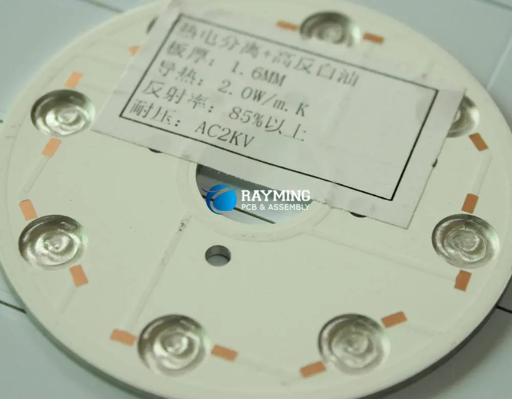
Printed circuit boards are without doubt the core materials for manufacturing electronic devices. There are several PCB manufacturers today as the use of these boards has become popular. Bergquist PCB is a high-quality PCB with great properties. Bergquist PCB features great flame-retardant, exceptional mechanical strength, and dimension stability.

Asides from that, this PCB features a good heat sink and electromagnetic protection.  Bergquist gap filler is a material that features great benefits for engineers. In this article, we will be discussing everything you need to know about Bergquist PCB.  

Bergquist PCB – What Does It Mean?

Bergquist PCB is a laminate class with aluminum base copper. This laminate features great thermal and mechanical properties. Bergquist thermal clad provides a thermal management solution for applications.  Especially those in need a high watt-density surface mount.

This thermal clad laminate conducts heat more. This substrate features better mechanical properties than direct bond copper constructions. It can remove components and enable the production processes of smaller devices.

Bergquist MCPCB features optimum durability, lower operating temperatures, and longer component life. Bergquist thermal clads aren’t only incorporated with metal base layers. These substrates can boost their function by replacing FR-4 in multilayer assemblies. The thermal clad’s thermal performance can reduce the copper circuit layerโ€™s thickness.

Bergquist thermal clad PCB allows low-cost manufacturing. This happens by removing the need for expensive manual assemblies.

Rayming Support BERGQUIST thermal clad material list :


1.bergquist Thermally Conductive Silicone Film Series ๏ผˆSil Pad= SILPADTSP๏ผ‰
SilPad400S๏ผˆSILPADTSP900๏ผ‰ใ€SilPad800๏ผˆSILPADTSP1600๏ผ‰ใ€SilPad900S๏ผˆSILPADTSP1600S๏ผ‰ใ€SilPad1200๏ผˆSILPADTSP1800๏ผ‰ใ€SilPadA1500๏ผˆSILPADTSPA2000๏ผ‰ใ€SilPad2000๏ผˆSILPADTSP3500๏ผ‰ใ€SilPadK10๏ผˆSILPADTSPK1300๏ผ‰ใ€SilPadK4๏ผˆSILPADTSPK900๏ผ‰ใ€SilPadK6๏ผˆSILPADTSP1100๏ผ‰
Abbreviation: SP400S/SP800S/SP900S/SP1200/SPA1500/SP2000/SPK4/SPK6/SPK10


2.bergquist Thermal silica film series ๏ผˆGap Pad= GAPPADTGP๏ผ‰
GapPadVo๏ผˆGAPPADTGP800VO๏ผ‰ใ€GapPadVoSoft๏ผˆGAPPADTGP800VOS๏ผ‰ใ€GapPadVoUltraSoft๏ผˆGAPPADTGP1000VOUS๏ผ‰ใ€GapPad1500๏ผˆGAPPADTGP1500๏ผ‰ใ€GapPad1500R๏ผˆGAPPADTGP1500R๏ผ‰ใ€GapPad2000S40๏ผˆGAPPADTGP2000๏ผ‰ใ€GapPad3000S30๏ผˆGAPPADTGP3000๏ผ‰ใ€GapPadHC3.0๏ผˆGAPPADTGPHC3000๏ผ‰ใ€GapPad2500S20ใ€GapPad5000S35๏ผˆGAPPADTGP5000๏ผ‰ใ€GapPadHC5.0๏ผˆGAPPADTGPHC5000๏ผ‰
(Abbreviation: GPVO, GPVOSOFT, GPVOUS, GP1500, GP2000S40, GP1500R, GP3000S30, GPHC3.0, GP2500S20, GP5000S35)


3.bergquist Thermally conductive solid glue series double grouping (GapFiller= GAPFILLERTGF):
GapFiller1000๏ผˆGAPFILLERTGF1000๏ผ‰ใ€GapFiller1500๏ผˆGAPFILLERTGF1500๏ผ‰ใ€GapFiller2000๏ผˆGAPFILLERTGF2000๏ผ‰ใ€GapFiller3500S35๏ผˆGAPFILLERTGF3600๏ผ‰ใ€GapFiller4000๏ผˆGAPFILLERTGF4000๏ผ‰๏ผˆGF1000ใ€GF1500ใ€GF2000ใ€GF3500S35ใ€GF4000๏ผ‰


4. bergquist phase change material series (Hi Flow = HIFLOWTHF):
HiFlow105, HiFlow225UT, HiFlow300P (HIFLOWTHF1600P)
5.bergquist Thermally conductive double-sided adhesive series (Bond Ply):
BondPly100ใ€BondPly400ใ€BondPly800๏ผˆBP105/BP108/BP111/BP400๏ผ‰

Benefits of Bergquist Thermal Clad PCB

bergquist thermal clad

There are several benefits of the Bergquist thermal clad. These benefits include:

Increased performance and durability

Bergquist PCB feature low thermal impedance which outperforms other insulators. This allows cooler operation. These thermal clad PCBs increase the level of durability. This is because the designs are simple and components are cool.

The thermal clad removes the thermal interface and uses thermal solder joints. This makes the assemblies cool.  These thermal clad PCBs allow automated pick-and-place for SMD’s which minimize production costs.

Board size reduction and hardware replacement

Bergquist thermal clad minimizes board space and replaces other components like heat sinks. It also helps to get rid of rubber or mica insulators under power devices. Heat transfer becomes better when it removes this hardware.

With the use of etched traces on the board, interconnects can be removed. This thermal clad helps to replace discrete devices at the board level.

Increased power density: The use of Bergquist PCBs allows more efficient electricity conduction. This means that these metal PCBs can conduct more efficient power.

Long term reliability

In the PCB world, new materials often go through a thorough qualification program. After this program, these materials can be launched in the market. Bergquist Company features state-of-the-art test facilities. It ensures that all their materials go through extensive testing. This is to verify their electrical integrity. Bergquist makes use of strict development procedures.

This U-L-approved company has ISO 9001:2000 certified production facilities.  Qualification testing includes temperature recycling, electrical and thermal stress.  It also involves adhesion and mechanical property validation. Bergquist combines up-front qualification tests with audits. This helps to ensure the materials offer consistent performance. Electrical testing takes place at selected intervals.

Extends dies life: One great thing about Bergquist PCB is that it prolongs dies shelf life. These PCBs guarantee you the componentsโ€™ life extension. This company ensures the fragile components are replaced. This is with more durable and stronger parts.

Bergquist Thermal Clad PCB Applications

Bergquist thermal clad are useful in several applications. This is because of their thermal and mechanical properties.

Motor drives: Bergquist thermal clad are ideal for use in motor drive applications. These thermal clad are good dielectric material and feature high watt density. With these materials, you can fabricate and install form factors into motor drives. The compact motor drives on these thermal clad ensure high watt density. Bergquist PCBs are ideal for high-temperature applications.

Power Conversion: Bergquist thermal clad is a preferred choice for engineers. This is because of its watt-density and size. This material features various thermal performances and is highly reliable. You can utilize this thermal clad in most form factors. Engineers also fabricate it in various substrate metals and copper foil weights. Bergquist sil pad is another material useful in this application.

LEDs: Thermal clad has been useful in LED applications for a long time. It is without a doubt that this material features great thermal properties. It is an ideal solution for designers who are considering reliability and quality. Bergquist thermal clad can be used for special bends and shapes. This enables the designer to make use of LED light engines in any application.

Heat-rail and forming: Thermal clad has become popular in heat-rail and forming. The use of this material has increased. It is used in other applications like automotive. Fabricators can remove the dielectric and form the metal with three-dimensional substrate. This material provides surface mount assemblies. It also gives attachment abilities in heat rails and forming applications.

What Does a Thermal Clad Comprise of?

FULL PCB MANUFACTURING Quote

This material is a dielectric metal base that features a bonded copper. Bergquist thermal clad consists of three different layers.

Dielectric layer: Bergquist thermal clad consists of a dielectric layer. This layer is at the middle of the clad and it ensures electrical isolation. Furthermore, this dielectric layer helps to minimize thermal resistance. This layer also provides electrical isolation. Any dielectric layer should be glass-free. This helps the thermal performance of the thermal clad.

This layer is the major element of Bergquist thermal clad. It bonds the circuit metal with the base metal together. Dielectric layers of a thermal clad sets the foundation. One great benefit of this layer is that it is U.L-certified.

Circuit layer: During the fabrication of a thermal clad, the circuit layer is the top layer. The circuit layer allows heat transfer and electric current conduction. For a thermal clad, there are various sizes of circuit layers. This size is between 0.5 oz and 10 oz. Furthermore, you can request a specific size that suits the intended application.

Base layer: The base layer is often made of aluminum. But, copper can also be used. The thickness of the material also varies. 1.57mm is the most common base material thickness. Designers are free to decide the thickness of this base layer. Ensure you select a base layer thickness that is ideal for your applications. Some applications donโ€™t need base layer materials.

What to Consider When Choosing Dielectric Materials

When choosing dielectric materials, you have to consider some factors. You will need to evaluate your options and consider the application requirements. We will be discussing the primary factors you should consider.

Thermal conductivity: This is an important factor you should not overlook. The Bergquist thermal cladโ€™s thermal conductivity clad determines thermal performance. This is important especially when interfacial area and resistance are considered.

Thermal Impedance: This helps to determine the watt density of any application. This is because thermal impedance measures how temperature declines. This decline is checked across each wattโ€™s stack-up. Lower thermal impedance indicates that more heat moves out of the components.

Dielectric layer type: It is no doubt that a dielectric layer is very important in a thermal clad. This dielectric layer helps to increase an applicationโ€™s performance. This layer is a ceramic/polymer combination. It makes thermal clad have great properties of electrical isolation.  

Polymers are great materials that can withstand high bond strengths and thermal aging. The ceramic filler helps to boost thermal conductivity. High-frequency applications need the best dielectric material.

Electric isolation: The thickness of dielectric material falls within a range. This is from 0.003 inches to 0.009 inches. Your isolation requirement will determine the thickness of your dielectrics. It is important you choose the right thickness for your dielectric material.

How to Measure the Thermal Conductivity of a Thermal Clad

bergquist material

Bergquist thermal cladsโ€™ thermal conductivity determines a lot of things. There are two major ways to know this materialโ€™s thermal conductivity. The value of the thermal conductivity can vary. This depends on the method you use.

Standard test method:

This method uses ASTM E1461 and ASTM D5470. The steady-state method is ASTM D5470. This method doesnโ€™t utilize approximations. More so, it offers derived value. Engineers refer to ASTM E1461 as the diffusivity of Laser Flash. You calculate thermal conductivity and the thermal diffusivity refers to the test output.

Non-standard method: 

Non-standard test methods are another way to determine thermal conductivity. When you use this non-standard method, the thermal conductivity values can be different. For example, if you select the same dielectric methods, then you can get different values.

You can utilize other substrateโ€™s materials. This will help you arrive at different results. It is important to know that this method doesnโ€™t give the best results of thermal conductivity.

Connection Techniques for Bergquist PCB

There are several connection techniques used on Bergquist PCB. These techniques are discussed below:

Power connections:

 Power connections are lead frame assemblies. This connection attaches to the printed circuit pads. Engineers bend these assemblies to give room for the shell utilized for encapsulation.  Some designs employ a plastic retainer ideal for high amperage. You will need to adhere to design rules and regulations for IMS PWBs.

Wire bonding: 

This is very important in designing packages that feature Chip-On-Board architecture. Wire bonding is a connection technique that utilizes the surface mount ability of a PCB.

Pin Connectors: 

In thermal clad assembly, pin headers and pin connectors are very useful. These connections are important when you attach an FR-4 panel to a thermal clad assembly. The most developed designs make use of stress relief when fabricating the pin. You can achieve current carrying capacity when you make use of redundant header pins.

Custom connectors: 

Custom connectors address mechanical and electrical fastening. The holes enable great soldering without errors. In addition, the shoulder washer helps the base plate. Custom connectors are not available commercially. Most times, they are custom-made.

Edge connectors:

Designers should finish the interfacing conductors with sulfamate nickel plating. This is very important when the edge connectors are part of the printed wiring pattern of the thermal clad. A 45-degree chamfer is the best for an edge connector. To avoid shorting, always sustain the minimum edge to conductor distance.

Considerations for Base Metal Layer Design

For the base layer of Bergquist thermal clad, there are certain considerations to look at.

Solder joints & the thermal expansion coefficient

Designers can reduce solder joint stress in a thermal clad. Select the appropriate base layer to match the expansion of the component to get this. The fatigue the solder joint undergoes in cycling or power is a major concern.

Cooling and heating may stress the joint. Solder joints are not rigid in terms of their mechanical capability. Mismatched materials, large devices, and extreme temperature may cause strain on solder joints.  Device termination and ceramic-based components are causes of solder joint fatigue.

Electrical connections to the base plate

Copper is an ideal material for the layer if the connection to the base plate is important. You should match the base and circuit coefficients of thermal TCE expansion. Failure to do this may cause excess plated-hole fatigue during thermal cycles.

The baseโ€™s thickness

For aluminum and copper thermal clad, there is a standard thickness of the gauge. There are also non-standard thicknesses. The base layerโ€™s thickness is an important factor to consider.

Heat spreading

For Bergquist thermal clad, copper and aluminum are the most common base layers. However, there are other metals you can utilize. Some applications consider CTE mismatch as a factor and as such, use other metals.

Costs

Without any doubt, copper and aluminum are cost-effective base layers. These materials are the industry standards. When design consideration is a factor, copper is the right option. Copper is costlier than aluminum. For instance, an aluminum material of 0.125 has similar costs to a copper of 0.040 inches.

Surface finish

This is another important consideration for the base metal layer design. Copper and aluminum base layers feature similar quality brushed surfaces. Aluminum comes in different colors such as blue, clear, red, and black.

How to Select a Circuit Layer

There are factors you should consider when selecting a circuit layer. The circuit layer of Bergquist material is very important. We will discuss these factors in this section.

Heat spreading capability

In materials of thermal clad, the dielectric thickness affects the way heat spreads. The foil thickness also influences heat spreading ability. Heat spreading is a great advantage. This can increase when you increase the thickness of the copper conductor. When the copper conductor thicknesses increase, it reduces junction temperature.

Engineers use heavy copper with bare die to remove any need for a packaged component. Sil pad 400 helps to isolate the sources of power from heat sinks.

Current carrying capabilities

This is an important consideration in selecting a circuit layer. In a thermal clad, the circuit layer represents the component-mounting layer. This layer interconnects the assemblyโ€™s components. The circuit trace that links up the components can convey greater currents. This is because it can dissipate heat.

Considerations for Electrical Design

There are several things that play a significant role in an electrical design of a thermal clad. These things include:

Proof Test

Proof testing is an important aspect. After the fabrication of PCBs, engineers ensure these materials undergo rigorous testing. The essence of proof testing is to ensure there are no defects in the materials. The materials for thermal clad usually undergo testing. This is to confirm the potency of the dielectric material. For testing the voltages need to be higher than the beginning of partial discharge.

Experts suggest that the number of proof tests should be at a minimum. This will help to prevent some issues from occurring.
Partial discharge includes the following:

  • Surface tracking and treeing
  • Surface emission at interfaces
  • Inner discharges in cavities or void
  • Corona discharge

During the proof test, engineers test several circuit boards at once. Proof test helps to ascertain that the dielectric insulation has no degradation. Degradation can occur due to any defects in the material or the fabrication process.

The proof testing at some voltage levels can reduce the life span of the dielectric. Poof testing above 1200 or 700 VAC shows defects in the dielectric insulation of the material.

Micro-voids, delaminations, and micro-fractures in the dielectric can break down during the test. Experts recommend using the DC proof test to ensure safety. The levels of voltage should be around 1500 VDC to 2250 VDC.
You have to control the voltage’s ramp to prevent tripping. This will also help to control the test effectively.

Operators have to take safety considerations during DC testing. They must ensure that the board is fully discharged before they remove it from the test fixture.

Breakdown Voltage

Dielectric breakdown voltage refers to the possible difference that dielectric failure can happen. Dielectric failure may happen in an insulating material between two electrodes. Such breakdown is irrecoverable and permanent. ASTM maintains that the results from this test can help to detect the dielectric characteristics of a material.

This is different from the proof test. Experts recommend proof testing below 50% of the actual dielectric breakdown voltage. It as well involves providing for creepage distance to prevent surface arcing.

Hipot testing

Dielectric materials come in different thicknesses and types. Not all boards yield the same result. During Hipot testing, metal substrates that are insulated look like capacitors of parallel plates.

The value of the capacitance varies. This difference is with the configurations of board layouts and materials. This happens when a board passes the tests and another fails. However, both boards pass when you test for their leakage current and dielectric strength in a controlled environment.

It is very important to consider material characteristics when testing parameters. Parameters and test setup that don’t consider the necessary factors can cause false failures of the board.
The charge and leakage current is another test characteristic that raises concerns.  You can only detect leakage current measurements once you bring the board to DC voltage.

Read about Multilayer PCB here

How to Choose Dielectric Materials for Thermal Clad PCBs

Bergquist thermal clad uses dielectric materials that feature great properties. However, when choosing these dielectric materials, Bergquist considers certain factors. These factors include:

Peel strength:

Now, Peel strength of thermal clad works in line with the temperature you expose them to. Peel strength measures the strength of the bond between the dielectric material and copper conductor.

When the temperature rises, the peel strength of a thermal clad is weaker. The temperature of the thermal clad application will determine the peel strength.

Coefficient of thermal expansion: 

The operating environment of thermal clad will determine the coefficient of thermal expansion. This value increases with the temperature.

Storage modulus:

The temperature of the operating environment determines a lot. It doesnโ€™t only determine the peel strength and CTE, but it also determines storage modulus. When there is an increase in temperature, the storage modulus decreases. You can choose the ideal Bergquist material for your operating environment.

Frequently Asked Questions

What factors determine the cost of Bergquist thermal clad? The cost of a Bergquist thermal clad varies. Several factors determine the cost of these materials. The material quality plays a significant role in the cost of this thermal clad. Aluminum and copper are the best materials for the base layer.

The size of the material also determines the cost. If the aluminum or copper is bigger, the cost will be higher. The materialโ€™s thickness is also an important factor. These factors determine the price of the thermal clad.

What are the risks of operating Bergquist thermal clad above glass transitions? The mechanical and electrical properties of this thermal clad will change. You will notice that the CTE increases and the peel strength reduces. The storage modulus of the thermal clad also declines.

What is the ideal operating temperature of a Bergquist PCB? The type of dielectric will determine bergquist PCBsโ€™ operating temperature. If you will utilize this PCB in high-temperature applications, HT Bergquist PCB is the best.

What does a Bergquist gap pad do? A Bergquist gap pad is a material that helps to fill the air gaps between devicesโ€™ heat spreaders. It offers a thermal interface between devices and heat sinks.

Conclusion

Bergquist material features great thermal and electrical properties. This material is ideal in several high-temperature applications. The dielectric material of Bergquist PCB plays a significant role. Henkel Bergquist is gaining popularity in the PCB industry.

Bergquist produces electrical and mechanical stable thermal clad. Bergquist PCB has its unique benefits and this makes it stand out in the industry.

What is Xilinx XC6SLX25-3CSG324i FPGA ?

Xilinx XC6SLX25-3CSG324i

Introduction

The Xilinx XC6SLX25-3CSG324i is a mid-range Spartan-6 series FPGA (Field Programmable Gate Array) chip optimized for cost-sensitive, high-volume applications. This article provides an overview of the XC6SLX25 FPGA including its key features, internal architecture, available development boards and example applications.

FPGA Overview

An FPGA is an integrated circuit containing programmable logic blocks and interconnects that can be configured to implement custom hardware functions. Unlike Application Specific Integrated Circuits (ASICs), the functionality of FPGAs can be changed as needed by reprogramming.

Key characteristics of FPGAs:

  • Contains configurable logic blocks (CLBs) to implement logic
  • I/O blocks provide interfacing capability
  • Interconnects route signals between logic and I/O
  • SRAM based configuration for reprogramming
  • Much lower cost compared to ASICs

This field programmability makes FPGAs ideal for fast prototyping and flexible designs.

XC6SLX25-3CSG324i Overview

The Xilinx XC6SLX25-3CSG324i FPGA has the following key features:

  • Spartan-6 mid-range FPGA series from Xilinx
  • Optimized for low-cost, minimal power consumption applications
  • 324 pin ceramic fine line surface mount CSP (chip scale package)
  • 23,038 logic cells featuring 6-input LUTs
  • 136 18Kb block RAMs
  • 8 Digital Clock Managers (DCMs)
  • 240 DSP48A1 slices with 18×18 multipliers
  • 3.2 Gbps low-power transceivers
  • Multi-voltage support 1.0V to 1.8V VCCINT/VCCAUX
  • -3 speed grade

With these specs, the XC6SLX25 FPGA offers an optimal balance of logic capacity, low cost and minimal power for space-constrained embedded applications.

Internal Architecture

The XC6SLX25 contains the following key components in its internal architecture:

Configurable Logic Blocks

The basic building block is the Configurable Logic Block (CLB) which contains:

  • 4-input LUTs for logic implementation
  • Flip flops for registering logic
  • Fast carry logic for arithmetic

CLBs are arranged in a two-dimensional array across the chip.

Block RAM

136 Kb (18K x 8) of true dual-port block RAMs distributed through the array provide local memory with two independent ports.

DSP Slices

DSP48A1 slices allow digital signal processing operations like MAC, multiply accumulate, multipliers, adders, logical functions.

Clock Management

8 DCMs provide clock synthesis, skew adjustment, jitter filtering and other clocking support.

I/O Blocks

Periphery IOBs feature support for common I/O standards like LVCMOS, LVDS, and SSTL. High speed GTP transceivers allow serial interfacing.

Interconnect

A flexible routing architecture connects internal components and IOBs using a combination of local, direct, global and long line interconnects spanning multiple channels.

Development Tools and Kits

Xilinx offers a full ecosystem of development tools and boards to support designs using the XC6SLX25 FPGA:

Software Tools

  • ISE Design Suite – For synthesis and place and route
  • Xilinx Platform Studio – GUI for constraint entry
  • ChipScope – Integrated logic analyzer
  • EDK – For Microblaze embedded processor development

Evaluation Kits

  • SP601 evaluation board – Features XC6SLX25 in UFBGA package, DDR2 memory, FMC connector etc.
  • SP605 board – Contains XC6SLX25 FPGA with HDMI, VGA, Ethernet etc.
  • KC705 board – Kintex-7 FPGA board also usable for Spartan-6 designs

Using these software tools and kits accelerates development and debug when leveraging the XC6SLX25 FPGA.

Applications

The optimal blend of low cost, power efficiency and logic capacity in the XC6SLX25 FPGA make it suitable for a wide range of applications including:

  • Battery powered embedded devices
  • Industrial automation and control
  • Wireless sensor systems
  • Automotive driver assistance systems
  • Space avionics
  • Video/image processing systems
  • Defense electronics
  • Test and measurement equipment
  • IoT endpoints

The XC6SLX25 allows implementing custom logic and algorithms for these applications in a small form factor.

Comparison with Other FPGAs

The XC6SLX25 sits in Xilinx’s low cost Spartan-6 FPGA series in terms of density and features. Comparisons with other major FPGA families are:

FPGAKey Characteristics
Xilinx Spartan-7Denser and higher performance successor to Spartan-6
Intel Max-10Competitor low-cost FPGA comparable to Spartan-6
Xilinx Artix-7Mid-range density and performance above Spartan-6
Xilinx Kintex-7High-end FPGA family for very demanding applications

Conclusion

The Xilinx XC6SLX25-3CSG324i FPGA provides a balance of low cost, power efficiency and logic capacity well suited for space-constrained embedded devices. The Spartan-6 architecture offers essential embedded peripherals like block RAM and DSP slices in an optimal configuration for control and interfacing applications. With the available software tools and development boards, the XC6SLX25 FPGA enables rapid prototyping and deployment of custom hardware designs.

FAQs

What are the key differences between Spartan-6 and Spartan-7 FPGAs?

Spartan-7 offers higher density, performance and bandwidth compared to Spartan-6. Key improvements include higher LUT counts, wider block RAM, PCIe support, and faster transceivers.

What embedded peripherals are integrated in the XC6SLX25 FPGA?

Embedded peripherals in XC6SLX25 include 136 Kb block RAMs, 240 DSP slices, 8 clock management tiles, 3.2 Gbps transceivers, among other dedicated hardware blocks.

What PCB packages can the XC6SLX25 be manufactured in?

XC6SLX25 is available in multiple packages including 324-pin CSP, 484-pin FFG900 and 13×13 mm UFBGA. PCB assembly methods supported include surface mount and socketing.

What are the typical power consumption figures for the XC6SLX25 FPGA?

Typical static and dynamic power consumption is low – in the range of 100 mW – due to Spartan-6 power optimization features. Exact power depends on utilization.

Which software tools can be used to develop applications with the XC6SLX25?

Xilinx offers the ISE Design Suite for synthesis and place-and-route. Soft processors like MicroBlaze can be implemented using Xilinx EDK tools. Simulation, debug and analysis is enabled by ChipScope.

All About Xilinx XC6SLX25-3CSG324i

The Xilinx XC6SLX25-3CSG324i is an IC readily available in different grades of speed. The highest possible speed is -3 and the highest performance too. The AC and DC parameters of the IC which is utilized for defense and automotive industries are equivalent to that of ICs used for commercial purposes. The characteristics of timing for the commercial ICs with the speed of -2 grade are equivalent to that of the ICs used for commercial purposes with the same grade. However, the speed grades of -3Q and -2Q are dedicatedly utilized for the applications where there are requirements of an expanded range of temperature Q.

The characteristics of timing are the same when speed is considered for both -3 and -2 grade ICs. The characteristics of both AC and DC are dedicated to the industrial, commercial, and expanded ranges of temperature. However, specified grades of speed and devices are expected to be readily available for the expanded or industrial ranges of temperature when it comes to the ICs of defense and automotive type. The reference to any of its device names is referring to the availability of all variations of its part number. But, the -3N grade of speed is designating all of the devices that are not supporting MCB functioning. The specifications of junction temperature and entire supply voltage is a representation of the worst possible case conditions and its parameters are encompassing the most typical and common designs for various applications.

Absolute Maximum Conditions

If stress is applied beyond the rated absolute maximum rating to the device may result in its permanent damage or burnout. The stress ratings are necessary for the device to be operational and it may not perform if such conditions are not fulfilled for its operation. Furthermore, if the device is exposed to the absolute maximum ratings too frequently may also result in any irreversible damage to the device. When the eFUSE of the device is programmed, it requires a current of up to 40mA and its VFS may be in the range of 3.45V to 0V. The overshoot duration of the input/output absolute maximum limit is in the percentage of the data for that period when 3.45V is applied. The maximum possible overshoot of voltage is 4.40V. The maximum bearable temperature for soldering purposes is Tsol for the device.  

Recommended Operating Conditions

FULL PCB MANUFACTURING Quote

The entire range of voltages is relevant to the position of the ground or GND. To perform the device in its extended performance range while not utilizing the standard VCCINT range of voltages. But the VCCINT is not recommended to be utilized for designs that are not using MCB, LX4 devices, devices of CPG196 packages or TQG144, and -3N grade of speed. The maximum possible voltage droop VCCAUX is about 10 millivolts per milliseconds. In case when the configuration is underway, when VCCO_2 is about 1.8V then its VCCAUX must be around 2.5V. When the device of -1L is requiring VCCAUX to be 2.5V through the use of standard RSDS_33, RSDS_25, LVPECL_25, LVDS_25, PPDS_25, and BLVDS_25 input/output on its inputs then LVPECL_33 is not supposed to be implemented at -1L devices.

The configuration data is always retained by the device even in case if the VCCO is dropped to 0V and the device has the inclusion of VCCO for 3.3V, 2.5V, 1.8V, 1.5V, and 1.2V respectively. The receiver and transmitter are required to have a common supply for VCCO when it comes to the PCI system. Xilinx PCI IP is not supported by the devices with -1L speed. 100mA must not be exceeded per bank for the device. Maintenance of VBATT is also necessitated for RAM backed by the battery when the VCCAUX is not being applied. When the VCCAUX is applied to the device then VBATT could be disconnected.

eFUSE Programming Conditions

The programming of eFUSE is only supported with the help of JTAG and such specifications are only applied while programming of the AES key of eFUSE. While programming the eFUSE, it must be guaranteed that VFS is lesser or equivalent to VCCAUX. While when the eFUSE is not programmed or is not in use, it is recommended that GND and VFS must be connected. But VFS must be in the range of 3.45V to 0V. There is a requirement of a resistor RFUSE for programming the AES key of eFUSE.

Recommended DC Characteristics

The measurement of the CIN is representing using a pad of die capacitance and not including package. The maximum possible value which is specified for the worst case is processed at 25 degrees Celsius. Referring to the RDT variation IBIS model and for values at VCCAUX of 2.5V, then IBIS values of RDT seem valid for all of the ranges of temperature. Whereas, there is no requirement of VCCO2 for retention of data. The minimum value of the VCCO2 for configuration and powering on reset is about 1.65V.

Quiescent Current

The specification of conventional values for the quiescent supply current of the device is done at nominal voltage and junction temperature of 25 degrees Celsius. The devices which are used for industrial and commercial grades are also having the same values. But, its higher values are lying at 100 degrees Celsius. Xilinx XC6SLX25-3CSG324i is recommending the analysis of static power consumption through the use of power estimator software. The nominal value of VCCINT is around 1.2V and is computed through the use of the XPE tool. The typical values are often used for devices that are blank and have no pull-up resistors in their active state, no output current loads, and all input/output pins are floating and in 3-state. In case if differential signaling is utilized then the values of quiescent current can be made more precise through the utilization of XPA software.

Ramp Time of Power Supply

The minimum requirement for VCCO2 for its reset on powering-on along reconfiguration is 1.65V. The device is requiring a specific amount of supply current while powering on to ensure the initialization of the device properly. The consumption of actual current is dependent on the rate of power on the ramp for its power supply. XPA or XPE tools are utilized for estimation of the drain currents for the power supplies.

PIC Microcontroller Guide: PIC16F877A, PIC18F, dsPIC33, and More

PIC Microcontrollers

I. Introduction to PIC Microcontrollers

In the world of embedded systems and electronics, PIC microcontrollers have become a cornerstone of innovation and development. These versatile chips, often referred to as PIC micros, PIC controllers, PIC MCUs, or PIC chips, have revolutionized the way we approach electronic design and automation.

What is a PIC Microcontroller?

A PIC microcontroller is a small, integrated circuit designed to perform specific tasks in embedded systems. PIC stands for Peripheral Interface Controller, which hints at its primary function โ€“ to control various peripherals and interfaces in electronic devices.

Brief History and Evolution

PIC microcontrollers were first introduced by Microchip Technology Inc. in the mid-1980s. Since then, they have undergone significant evolution, with each new generation bringing improvements in processing power, memory capacity, and peripheral features. Today, PIC microcontrollers are among the most widely used MCUs in the industry, powering everything from simple hobby projects to complex industrial systems.

Importance in Embedded System Design

The importance of PIC MCUs in embedded system design cannot be overstated. They offer a perfect balance of performance, cost-effectiveness, and versatility, making them suitable for a wide range of applications. From consumer electronics to automotive systems, PIC microcontrollers play a crucial role in bringing intelligence to everyday devices.

II. Understanding the PIC Architecture

To fully appreciate the capabilities of PIC microcontrollers, it’s essential to understand their underlying architecture and the advantages it brings to embedded system design.

General Architecture of a PIC Processor

PIC microcontrollers are built on a solid architectural foundation that contributes to their efficiency and performance:

  1. Harvard Architecture: PIC MCUs use a Harvard architecture, which separates program and data memory. This allows for simultaneous access to both instruction and data memory, enhancing overall performance.
  2. RISC-based Design: PIC microcontrollers employ a Reduced Instruction Set Computing (RISC) architecture. This means they have a smaller set of instructions, each executed in a single clock cycle, leading to faster and more efficient processing.
  3. Memory and Peripherals: A typical PIC microcontroller includes various types of memory:
    • Flash memory for program storage
    • EEPROM for non-volatile data storage
    • RAM for temporary data storage
    Additionally, they feature a wide array of built-in peripherals such as timers, ADCs, PWM modules, and communication interfaces.

Advantages of PIC Microcontrollers

PIC microcontrollers offer several advantages that have contributed to their widespread adoption:

  1. Cost-effective: PIC MCUs provide a high level of functionality at a relatively low cost, making them accessible for both hobbyists and large-scale industrial applications.
  2. Low Power Consumption: Many PIC microcontrollers are designed with power efficiency in mind, making them ideal for battery-operated and energy-conscious applications.
  3. Wide Availability: With a vast range of models catering to different needs, PIC microcontrollers are readily available, ensuring that developers can find the right chip for their specific requirements.
  4. Robust Ecosystem: PIC microcontrollers benefit from a mature ecosystem of development tools, software libraries, and community support, making development easier and more efficient.

III. Key Families of PIC Microcontrollers

Microchip Technology offers a diverse range of PIC microcontrollers, each tailored to specific application needs. Let’s explore some of the key families:

A. PIC16 Series (8-bit)

The PIC16 series represents the backbone of 8-bit PIC microcontrollers, offering a perfect balance of performance and affordability. Within this series, the PIC16F877A stands out as one of the most popular and versatile options.

Focus on the PIC16F877A Microcontroller

The PIC16F877A has become a favorite among hobbyists and professionals alike due to its rich feature set and ease of use. Let’s delve into its key features:

  1. 8-bit RISC Architecture: The PIC16F877A uses an efficient 8-bit RISC core, allowing for fast execution of instructions.
  2. Memory: It offers 368 bytes of RAM and 256 bytes of EEPROM, providing ample space for data storage and program memory.
  3. I/O and Peripherals: With 33 I/O pins and 5 channels of 10-bit Analog-to-Digital Converters (ADC), the PIC16F877A is well-equipped for interfacing with various sensors and actuators.
  4. Communication Interfaces: It supports multiple communication protocols, including USART, SPI, and IยฒC, facilitating easy integration with other devices.
  5. Timer Modules: The PIC16F877A includes several timer modules, enabling precise timing control in applications.

Use Cases for PIC16F877A

The PIC16F877A finds applications in a wide range of projects, including:

  • Robotics: Controlling motors, sensors, and decision-making logic
  • Home Automation: Managing lighting, temperature control, and security systems
  • Educational Projects: Serving as an excellent platform for learning microcontroller programming
  • Industrial Control: Monitoring and controlling industrial processes

B. PIC18 Series (Advanced 8-bit)

The PIC18 series represents an evolution of the 8-bit PIC architecture, offering enhanced performance and additional features compared to the PIC16 series.

Key Features of PIC18 Microcontrollers

  1. Improved Performance: PIC18 MCUs offer higher clock speeds, typically ranging from 40 MHz to 64 MHz, allowing for faster execution of instructions.
  2. Enhanced Peripheral Set: These microcontrollers come with an expanded set of peripherals, including more advanced timer modules, enhanced PWM capabilities, and improved communication interfaces.
  3. Larger Memory: PIC18 series offers increased program and data memory, supporting more complex applications.
  4. C Compiler Optimized: The architecture is optimized for C language programming, making it easier to develop complex applications using high-level languages.

Applications of PIC18 Series

PIC18 microcontrollers are commonly used in:

  • Automotive Systems: Engine control units, body electronics, and infotainment systems
  • Industrial Control: PLC systems, motor control, and process automation
  • Consumer Electronics: Appliances, remote controls, and smart home devices
  • Medical Devices: Patient monitoring equipment and portable diagnostic tools

C. dsPIC30/dsPIC33 (16-bit Digital Signal Controllers)

The dsPIC series, particularly the dsPIC33, represents Microchip’s venture into the world of Digital Signal Controllers (DSCs). These devices combine the features of a microcontroller with the signal processing capabilities of a Digital Signal Processor (DSP).

Key Features of dsPIC33

  1. 16-bit Architecture: The dsPIC33 uses a 16-bit core, offering higher processing power compared to 8-bit PICs.
  2. DSP Capabilities: It includes hardware multipliers and accumulators for efficient digital signal processing operations.
  3. High-Speed Operation: Many dsPIC33 models can operate at clock speeds up to 150 MHz, enabling real-time processing of complex algorithms.
  4. Advanced Peripherals: dsPIC33 controllers often include specialized peripherals for motor control, power conversion, and high-speed communication.

Applications of dsPIC33

The dsPIC33 family is particularly well-suited for applications requiring both microcontroller functionality and signal processing capabilities:

  • Motor Control: Precise control of electric motors in industrial and automotive applications
  • Power Conversion: Digital power supplies and inverters
  • Audio Processing: Digital audio effects and sound processing in consumer electronics
  • Sensor Fusion: Combining data from multiple sensors in IoT and automotive applications

IV. Tools and Software for PIC Development

Developing applications for PIC microcontrollers requires a set of specialized tools and software. Microchip Technology provides a comprehensive ecosystem to support PIC development:

Popular PIC Programmers

  1. PICkit: A series of low-cost programmers ideal for hobbyists and small-scale development. The latest version, PICkit 4, offers support for a wide range of PIC and dsPIC devices.
  2. MPLAB ICD (In-Circuit Debugger): A more advanced tool that allows for programming and real-time debugging of PIC microcontrollers.
  3. MPLAB REAL ICE: A high-end in-circuit emulator for professional development, offering advanced debugging capabilities.

MPLAB X IDE and XC Compilers

  1. MPLAB X IDE: Microchip’s free, open-source Integrated Development Environment (IDE) for PIC development. It provides a user-friendly interface for writing, debugging, and managing projects.
  2. XC Compilers: A suite of C compilers optimized for different PIC families:
    • XC8 for 8-bit PICs
    • XC16 for 16-bit PICs and dsPICs
    • XC32 for 32-bit PICs

Simulators and Debuggers

  1. MPLAB Simulator: An integrated simulator within MPLAB X IDE, allowing developers to test code without physical hardware.
  2. Proteus: A popular third-party simulation software that supports various PIC microcontrollers and allows for virtual circuit design and testing.

Tips for PIC Microcontroller Programming

  1. Start with simple projects to familiarize yourself with the PIC architecture and development environment.
  2. Make use of Microchip’s extensive documentation and application notes.
  3. Utilize built-in peripherals whenever possible to optimize code efficiency.
  4. Implement proper debouncing techniques when working with buttons or switches.
  5. Use interrupt-driven programming for time-critical tasks.

V. Applications of PIC Microcontrollers

PIC microcontrollers have found their way into numerous applications across various industries. Their versatility, cost-effectiveness, and robust feature set make them suitable for a wide range of projects:

Consumer Electronics

  • Remote Controls: Many TV, air conditioning, and other appliance remotes use PIC microcontrollers for their operation.
  • Smart Home Devices: PIC MCUs power various IoT devices, from smart switches to environmental sensors.
  • Digital Clocks and Timers: PIC16 series chips are often used in digital clock applications.

Medical Devices

  • Blood Glucose Meters: PIC microcontrollers handle the data processing and display in portable glucose monitoring devices.
  • Digital Thermometers: PIC chips manage temperature sensing and display in digital thermometers.
  • Pulse Oximeters: PIC18 or dsPIC33 controllers process signals from optical sensors in these devices.

Industrial Automation

  • Programmable Logic Controllers (PLCs): PIC18 and dsPIC33 chips are used in compact PLCs for industrial control.
  • Sensor Interfaces: PIC microcontrollers handle data acquisition and processing from various industrial sensors.
  • Motor Control: dsPIC33 controllers are particularly suited for precise motor control applications.

IoT Projects

  • Weather Stations: PIC-based systems collect and transmit environmental data.
  • Asset Tracking: PIC microcontrollers manage GPS and communication modules in tracking devices.
  • Smart Agriculture: PIC chips control irrigation systems and monitor soil conditions in smart farming applications.

Real-World Devices Using PIC Chips

  1. Automotive Systems: Many car manufacturers use PIC microcontrollers in their engine control units, dashboard displays, and body electronics.
  2. Power Tools: Cordless drills and other power tools often use PIC MCUs for motor control and battery management.
  3. Fitness Trackers: Some fitness wearables employ PIC microcontrollers for data processing and power management.
  4. Vending Machines: PIC chips manage payment systems and product dispensing mechanisms in modern vending machines.
  5. Solar Inverters: dsPIC33 controllers are used in solar inverters for efficient power conversion and grid synchronization.

Read more about๏ผš

VI. Getting Started with PIC Development

For those new to PIC microcontrollers, getting started can be an exciting journey. Here’s a guide to help you set up your development environment and create your first PIC project:

Setting Up a Development Environment

  1. Installing MPLAB X IDE:
    • Visit the Microchip website and download the latest version of MPLAB X IDE.
    • Follow the installation wizard to complete the setup.
    • Install the appropriate XC compiler for your PIC family (XC8 for 8-bit PICs, XC16 for 16-bit PICs).
  2. Choosing a PIC Board: For beginners, it’s recommended to start with a development board. The PIC16F877A development board is an excellent choice due to its versatility and extensive documentation.

Writing Your First Program (Blinking LED Example)

Let’s create a simple program to blink an LED using a PIC16F877A:

 #include <xc.h>
#include <stdint.h>

// Configuration bits
#pragma config FOSC = HS // Oscillator Selection bits (HS oscillator)
#pragma config WDTE = OFF // Watchdog Timer Enable bit (WDT disabled)
#pragma config PWRTE = OFF // Power-up Timer Enable bit (PWRT disabled)
#pragma config BOREN = ON // Brown-out Reset Enable bit (BOR enabled)
#pragma config LVP = OFF // Low-Voltage (Single-Supply) In-Circuit Serial Programming Enable bit (RB3 is digital I/O, HV on MCLR must be used for programming)
#pragma config CPD = OFF // Data EEPROM Memory Code Protection bit (Data EEPROM code protection off)
#pragma config WRT = OFF // Flash Program Memory Write Enable bits (Write protection off; all program memory may be written to by EECON control)
#pragma config CP = OFF // Flash Program Memory Code Protection bit (Code protection off)

#define _XTAL_FREQ 20000000 // 20 MHz oscillator

void main(void) {
TRISB0 = 0; // Set RB0 as output

while(1) {
RB0 = 1; // Turn LED on
__delay_ms(500); // Wait for 500 ms
RB0 = 0; // Turn LED off
__delay_ms(500); // Wait for 500 ms
}
}

This program will cause an LED connected to pin RB0 to blink every second.

Programming the PIC Microcontroller

  1. Connect your PIC programmer (e.g., PICkit) to your computer and the development board.
  2. In MPLAB X IDE, create a new project and select your PIC model (PIC16F877A in this case).
  3. Copy the above code into the main source file.
  4. Build the project and program the PIC using the “Make and Program Device” option in MPLAB X IDE.

Congratulations! You’ve just programmed your first PIC microcontroller. This simple example demonstrates the basics of PIC programming, including port configuration, digital output, and timing delays.

VII. Choosing the Right PIC MCU for Your Project

Selecting the appropriate PIC microcontroller for your project is crucial for its success. Here are some factors to consider:

Factors to Consider

  1. Memory and Speed Requirements:
    • Assess the amount of program memory and RAM your application needs.
    • Determine the processing speed required for your tasks.
  2. Peripheral Support:
    • List the peripherals your project requires (e.g., ADC, UART, I2C, SPI).
    • Check if the MCU has the necessary number of I/O pins.
  3. Voltage and Power Considerations:
    • Determine the operating voltage of your system.
    • Consider power consumption, especially for battery-operated devices.
  4. Cost and Availability:
    • Balance the features you need with your budget constraints.
    • Ensure long-term availability for production projects.

Comparison Table: PIC16F877A vs PIC18F vs dsPIC33

FeaturePIC16F877APIC18F452dsPIC33FJ128GP802
Architecture8-bit8-bit16-bit
Max Clock Speed20 MHz40 MHz80 MHz
Program Memory8K x 14 words32K x 16 words128K x 24 words
RAM368 bytes1536 bytes16K bytes
EEPROM256 bytes256 bytesNone
ADC10-bit, 8 channels10-bit, 8 channels12-bit, 9 channels
I/O Pins333428
UART112
SPI/I2CYesYesYes
PWM2 channels2 channels6 channels
DSP CapabilitiesNoNoYes
Typical Use CaseGeneral PurposeAdvanced 8-bitMotor Control, DSP

This comparison illustrates the progression in capabilities from the 8-bit PIC16F877A to the more advanced 8-bit PIC18F452, and finally to the 16-bit dsPIC33FJ128GP802 with its enhanced processing power and DSP features.

VIII. Tips and Resources for PIC Enthusiasts

To help you on your journey with PIC microcontrollers, here are some valuable tips and resources:

Forums, Books, and Communities

  1. Microchip Forums: The official Microchip forums are an excellent place to ask questions and share knowledge with other PIC developers.
  2. Books:
    • “PIC Microcontrollers: Know It All” by Lucio Di Jasio
    • “Programming 8-bit PIC Microcontrollers in C” by Martin P. Bates
    • “Designing Embedded Systems with PIC Microcontrollers” by Tim Wilmshurst
  3. Online Communities:
    • Stack Overflow’s [pic] tag
    • Reddit’s r/PIC_Programming subreddit
    • EEVblog Forum’s Microcontrollers section

Recommended Starter Kits

  1. PICkit 3 Starter Kit: Includes a PICkit 3 programmer/debugger and a development board with various peripherals.
  2. PIC18F Starter Kit: A more advanced kit featuring a PIC18F46K22 MCU and multiple sensors and interfaces.
  3. dsPIC33 Motor Control Starter Kit: Ideal for those interested in motor control applications using dsPIC33 controllers.

Best Practices in PIC Microcontroller Design and Programming

  1. Use Timer Interrupts: For precise timing, rely on timer interrupts rather than delay loops.
  2. Implement Proper Debouncing: When using buttons or switches, implement software debouncing to prevent false triggers.
  3. Optimize Power Consumption: Utilize sleep modes and peripheral management to reduce power usage in battery-operated devices.
  4. Comment Your Code: Maintain clear and comprehensive comments in your code for easier maintenance and collaboration.
  5. Leverage Built-in Peripherals: Make use of built-in hardware peripherals whenever possible to offload tasks from the CPU.
  6. Keep Up with Documentation: Regularly refer to datasheets and errata to stay informed about device-specific features and limitations.

IX. Conclusion

The world of PIC microcontrollers offers a vast playground for both hobbyists and professionals in the field of embedded systems. From the versatile 8-bit PIC16F877A to the powerful 16-bit dsPIC33 series, these microcontrollers provide a scalable platform for a wide range of applications.

The PIC family’s strength lies in its diversity, offering solutions for simple control tasks to complex signal processing applications. Whether you’re building a home automation system with a PIC16F, developing an industrial controller with a PIC18F, or designing a high-performance motor control system with a dsPIC33, there’s a PIC microcontroller suited for your needs.

As we’ve explored throughout this guide, the ecosystem surrounding PIC microcontrollers is rich with development tools, resources, and community support. This comprehensive environment makes PIC MCUs an excellent choice for both learning and professional development.

We encourage you to explore the capabilities of PIC microcontrollers hands-on. Start with simple projects, gradually increase complexity, and don’t hesitate to experiment with different PIC families. The skills and knowledge you gain will be invaluable in the ever-evolving world of embedded systems and IoT.

Remember, the journey of mastering PIC microcontrollers is ongoing. Stay curious, keep learning, and most importantly, enjoy the process of bringing your ideas to life with these powerful little chips!

X. FAQ (for Featured Snippets and SEO Boost)

  1. What is the difference between PIC and other microcontrollers? PIC microcontrollers use a Harvard architecture and RISC instruction set, offering efficiency and speed. They are known for their wide range of options, from simple 8-bit to advanced 16-bit DSC models, and have a mature ecosystem of development tools.
  2. What is PIC16F877A used for? The PIC16F877A is a versatile 8-bit microcontroller commonly used in hobbyist projects, educational settings, and simple industrial applications. It’s popular for tasks like motor control, sensor interfacing, and basic automation due to its balance of features and affordability.
  3. How do I program a PIC chip? To program a PIC chip, you need:
    1. A PIC programmer (like PICkit)
    2. MPLAB X IDE and appropriate XC compiler
    3. Write your code in C or assembly
    4. Compile the code and use the programmer to flash it onto the PIC chip
  4. Is dsPIC the same as PIC? dsPIC is a subfamily of PIC microcontrollers. While regular PICs are general-purpose microcontrollers, dsPICs are Digital Signal Controllers that combine microcontroller features with Digital Signal Processing capabilities, making them suitable for more complex signal processing tasks.
  5. What is the best PIC programmer for beginners? The PICkit 3 or PICkit 4 is often recommended for beginners. These programmers are affordable, easy to use, and support a wide range of PIC microcontrollers. They also integrate well with Microchip’s MPLAB X IDE, providing a smooth development experience for newcomers.

Top 10 Flexible Printed Circuit Manufacturers in Israel

flexible printed circuit

Printed Circuit Boards (PCBs) are in high demand across different industries. The relevance of PCBs in the electronic manufacturing process cannot be underestimated.

Out of the different kinds of types of PCBs, one of them stands out. That is the flexible PCB. As a PCB consumer, you want to find the best flexible printed circuit manufacturers that will design and fine-tune your circuit board for the electronic application needs you may have.

Some of these flexible printed circuit manufacturers can be found in Israel. This article is your guide to finding the top 10 flexible circuit board manufacturers in Israel.

The 10 Best flexible printed circuit Manufacturers in Israel

flex circuit board manufacturers

We present to you, the top 10 manufacturers of flexible Printed Circuit Boards (PCBs) in Israel. We came up with this list after checking some of the circuit board offerings of these companies, as well as the receptibility of their services by flexible PCB consumers who had patronized them.

1. Trace PCB

Trace PCB is what you will call โ€œone of the best PCB design Bureaus.โ€ This is because of the specialist services the company offers as far as the production of Printed Circuit Boards (PCBs) are concerned.

Capabilities

Trace PCB was established over 2 decades ago and has been under constant evolution to keep up with the best practices and trends in the PCB market.

The company has in the last 28 years of existence, being able to develop and design circuit boards for different kinds of electronic products. These products have at different times, been deployed for use in advanced technologies.

Quality flexible printed circuit Production

Asides from that, Trace PCB has a lot to offer, as far as the designing and production of Printed Circuit Boards (PCBs) is concerned. One of such capabilities is the production and delivery of high-quality flexible PCBs within a short time.

Component Engineering

The engineering of the flexible PCB components is very important. This is why Trace PCB offers advice to PCB consumers on the best way to engineer the components of the Flexible Printed Circuit Boards (PCBs).

Advanced PCB Manufacturing Solutions

Trace PCB is also following the trend in the Printed Circuit Board (PCB) market, and continually leverages the same to create sustainable solutions.

One of the high points of its solutions is the ability to follow the latest PCB manufacturing technologies. The company does a swell job of implementing the capabilities and requirements in the latest PCB designs.

Types of PCB Designs Offered

Trace PCB offers different kinds of Printed Circuit Board (PCB) designs. These include:

Website:

2. Print Electronics

Some flexible printed circuit manufacturers donโ€™t believe in wasting more time than necessary when designing flexible circuit boards.

One of such manufacturers is Print Electronics. The company has done a great deal towards the reduction of the lead time and other associated time-dependent tasks in the PCB design process.

It is popular for being one of the most reliable time to market experts, especially because of the 24-hour production time.

Reasons to Choose Print Electronics

Here are some of the reasons why we think the flexible printed circuit services offered by Print Electronics are awesome:

Highest Flexible PCB Production Standards

The standard of the flexible PCB is one of the factors worth considering when choosing a flexible printed circuit manufacturer.

On its part, Print Electronics leaves up to expectations by offering the highest production standards for flexible circuit boards.

These standards are in place because the manufacturer (Print Electronics) makes consistent investments in the use of advanced equipment that aids the professional manpower of the employees.

The equipment is also used to support the production of any kind of Printed Circuit Board (PCB) development.

Mass Production

Print Electronics aims to design and produce flexible circuit boards within 24 hours. This is usually the case if you are placing for low volumes.

However, the manufacturer may need to reach out to its overseas partners if the flexible printed circuit orders are for mass production.

A Wide Range of PCB Production

Print Electronics also covers a wide range of circuit board productions. Some of the PCBs the manufacturer designs are flexible PCBs, rigid circuit boards, and rigid-flexible printed circuits.

Website:

semi flex pcb

3. Synersys Israel Ltd

Synersys Israel Ltd was founded in 2002 and has in the last 19 years, consistently provided innovative solutions in the area of integrated research and development services of multi-disciplinary systems and consultations for the hi-tech industry.

Synersys Israel Ltd has also expanded its tentacles to cover the design and production of Printed Circuit Boards (PCBs).

You will find out some of the contributions of the company towards the improvement of the flexible printed circuit market in Israel.

Hardware Design and Engineering

This is where a bulk of the Printed Circuit Board (PCB) developmental services offered by Synersys Israel Ltd are categorized.

Under the Hardware Design and Engineering aspect of its operations, Synersys Israel Ltd offers PCB production, including the production of flexible circuit boards.

The manufacturer also excels in other hardware design areas, such as Eco management, digital circuits, electronic boards modules, analog circuits, production files, power supply design, Design for Manufacturing (DFM), and high-density PCB design.

System Design and Development

Synersys Israel Ltd also offers System Design and Development. This is where you will get other important PCB solutions, such as field experiments, turnkey projects, complete system integration that includes software, hardware, and mechanics.

Synersys Israel Ltd also offers other PCB solutions here, including full documentation, subsystems/modules, system architecture design, and design documents preparations.

Website:

4. PCB Technologies

Some PCB manufacturers focus on providing solutions for specific types of Printed Circuit Boards (PCBs), while some other prefer to offer as many solutions as possible.

PCB Technologies belongs in the latter category because it specializes in the provision of all-in-one PCB solutions.

The manufacturer also handles all your PCB projects with care and ensures that you get value for your money.

Advantages of Partnering with PCB Technologies

So far, we have come up with some of the huge advantages of getting PCB Technologies to work on your flexible printed circuit projects.

These are some of the reasons why the manufacturer is worth considering for the job:

Commitment to Perfection

PCB Technologies has been offering PCB design and manufacturing solutions for the past 4 decades. The manufacturer is also at the top of its game because of its commitment to perfection.

Ideally, PCB Technologies manufactures different kinds of Printed Circuit Boards (PCBs) that have been used in both the aerospace and defense industries.

PCB Technologies also holds the AS9100 and Nadcap certified quality system that serves as a testament to the manufacturerโ€™s disposition to offering quality flexible printed circuit production.

flexible printed circuit Board Design

A lot of effort goes into the production of the flexible circuit board. This includes the selection of the flexible printed circuit material and the flexible printed circuit connectors.

PCB Technologies takes a lead here by offering a wide range of flexible printed circuit design solutions. These solutions include but are not limited to:

  • Assistance in planning-controlled impedance
  • Optimized choice of flexible printed circuit materials
  • Recommendations on โ€œDesign-to-Costโ€
  • Recommendations for review and testability of the flexible circuit board design.

Website:

5. Newline-PCB

FULL PCB MANUFACTURING Quote

Newline-PCB is dominating the Israeli PCB industry with the novel solutions it came up with. At the core of these solutions is the primary objective of the company, which is to specialize in imported Printed Circuit Boards (PCBs).

As a specialist in this field, Newline-PCB imports different kinds of Printed Circuit Boards (PCBs) and in different amounts.

It doesnโ€™t matter if you want a prototype of the flexible printed circuit, or you want to order for small or medium quantities of the circuit board. Rest assured that Newline-PCB can offer the services with ease.

Types of PCB Solutions

Newline-PCB imports different kinds of Printed Circuit Boards (PCBs), such as:

flexible printed circuit Solutions

These are some of the solutions or services that Newline-PCB offers to its flexible printed circuit customers:

Component Sourcing

Newline-PCB has an extensive list of circuit board suppliers both in Israel and in the Far East. So, it would be easier for the manufacturer to source or place orders for the flexible printed circuit materials to be used when designing your flex circuit board.

Circuit Board Testing

As a company that is interested in customer satisfaction, Newline-PCB does all it can to keep the customers happy.

One of the ways it does that is by checking the flexible printed circuits (and any other kind of circuit board) both visually and electronically before shipping.

Multiple Production Capabilities

Newline-PCB also does a great job of offering you a wide range of options to choose from when it comes to the production of flexible PCBs.

With these production capabilities, you can decide to choose between the small and mass production levels.

Website:

6. KaiZen Technologies

KaiZen Technologies is a reputable flexible printed circuit manufacturer in Israel. The company is popular for the provision of advanced technology and engineering solutions. These services are offered to the electronics industry.

Also, KaiZen Technologies takes care of most of the circuit board production process and offers professional advice to the customers, where necessary. For example, the company takes note of the customersโ€™ flexible PCB expectations and keeps the same in mind when engaging in mass production of the circuit boards.

Why You Should Choose KaiZen Technologies

KaiZen Technologies has a lot of services to offer you, as far as the provision of flexible printed circuit services is concerned.

These are some of the advantages of outsourcing your flexible printed circuit project to the manufacturer:

Unique Management

KaiZen Technologies is committed to satisfying the needs of its customers. This is why the manufacturer places a premium on the provision of the best customer experience.

This is actualized via the unique management of the flexible printed circuit project.

Increased Product Reliability

KaiZen Technologies prefers to work with the best flexible printed circuit material. The company also has contacts with some of the best components suppliers.

The idea is to use only the best flexible printed circuit materials that would go a long way to increase the reliability of the circuit board designs.

Short Timetable

KaiZen Technologies wants you to have your finished flexible printed circuit in the shortest time possible. The manufacturer uses a shorter lead time to design the circuit boards without compromising the quality of the designs.

A Wide Range of Services to Choose from

KaiZen Technologies also offers a wide range of circuit board production services. These services cut across:

  • Mechanical Designs, such as flex and rigid PCBs, box build ASSEMBLY, jigs, and testers.
  • Electronic Design, such as board layout (rigid and flexible PCBs), Inter Connection Diagram (ICD), Concept and block diagram, Power Integrity, and Schematic.
  • Operational support
  • New Product Introduction (NPI) support
  • Testability solutions
  • Thermal analysis
  • Redesign & reverse engineering
  • Product relocation
  • DFMA report
  • Product documentation

Website:

7. EDAIS Integrity Solutions Ltd.

EDAIS Integrity Solutions Ltd is one of the leading providers and distributors of Electronic Design Automation solutions. These solutions are supplied to the electronic system-design market in Israel.

EDAIS Integrity Solutions Ltd couldnโ€™t have got to this height and gained this kind of recognition if it werenโ€™t doing something worthwhile.

Thus, here are some of the advantages of partnering with EDAIS Integrity Solutions Ltd for your next flexible printed circuit project:

Real-Time PCB Design

EDAIS Integrity Solutions Ltd understands the relevance of a quick prototype โ€“ it helps the customer to see what the outcome of the flexible printed circuit would look like.

That is why the manufacturer offers a real-time PCB design. The quickened pace for the flexible printed circuit production is done in a way that the errors in the circuit board design would be picked off instantly during the signoff checks.

To do this, EDAIS Integrity Solutions Ltd uses the OrCAD to go from prototype to production in lesser time.

Flexible Manufacturing Options

EDAIS Integrity Solutions Ltd also offers customers flexible manufacturing options. This way, you will have more options to choose from when it comes to flexible PCB production.

The flexibility of EDAIS Integrity Solutions Ltd.โ€™s manufacturing options also helps in cutting down on the costs of manufacturing the circuit board. This is possible because the manufacturer tries its best to adapt its flexible printed circuit manufacturing solutions to the budget of the customers.

Website:

8. MILPCB

MILPCB is another Israeli flexible circuit board manufacturer that you may be interested to work with.

We will give you some of the reasons why it is a good idea to have MILPCB as the manufacturer of your flexible PCBs moving forward.

Robust PCB Services

MILPCB offers you robust circuit board services. These services include flexible PCB prototyping and flexible PCB production or manufacturing.

Fast Lead Time

Your flexible circuit board can be designed and produced in the shortest time possible, thanks to the fast lead time offered by MILPCB.

This applies to both the flexible PCB prototype and production.

Superior Customer Service

You want to contact the customer care department when you have some questions to ask or some complaints to make.

MILPCB is all ears via the provision of superior customer service that attends to your concerns and addresses any issues you may have in good time.

Competitive Pricing

Saving costs when producing a circuit board could be tricky. As much as you want to cut down on expenses, it might affect the PCB project, especially when the quality of the material is not assured.

However, MILPCB has a way of balancing the equation. The most popular strategy is to source flexible PCB components from offshore suppliers. With strong negotiations, MILPCB can get you the flexible printed circuit material at a reduced cost.

Quality Performance

The quality and performance of the flexible circuit board are also worth considering. You don’t have to worry about that because MILPCB knows how to get around it.

This Israeli flexible printed circuit manufacturer bolsters the quality performance of the flexible circuit boards by ensuring that each of the facilities in its network is carefully selected ahead of the PCB production.

Website:

9. Flexitech Avia Printed Electronics

Flexitech Avia Printed Electronics is one of the most reliable manufacturers of flexible Printed Circuit Boards in Israel.

The company specializes in using Thick Film Technology to design and manufacture different kinds of Printed Circuit Boards (PCBs), including flexible PCBs.

Why the Thick Film Technology?

Flexitech Avia Printed Electronics has many years of experience in PCB design. So, the manufacturer had a good reason for using the Thick Film Technology for PCB production.

According to the manufacture, the Thick Film Technology makes it simpler for it (Flexitech Avia Printed Electronics) to print and produce different kinds of components for circuit boards.

These components are thereafter used across different electronics sectors and multiple industries.

Worthy of mention is that the viability and sustainability of the Thick Film Technology are because of the integration of other elements. The technology is used alongside advanced and complex processes of selective metallization, machining, printing, and brazing.

Flexitech Avia Printed Electronics Flexible PCB Options

When it comes to the designing and production of flexible circuit boards, Flexitech Avia Printed Electronics has some options to offer.

First, Flexitech Avia Printed Electronics can manufacture custom-made flexible Printed Circuit Boards (PCBs) for you. This would, in turn, be used as connectors in various applications where space-saving and flexibility are required.

Second and most important, the custom-made flexible printed circuits made by Flexitech Avia Printed Electronics can be stacked in various configurations. Most of these configurations would be ideal for both high-flex and dynamic applications.

Quality Assurances

The quality of the flexible printed circuits manufactured by Flexitech Avia Printed Electronics is also assured. This is because of the ISO 9001 standard that the manufacturer operates.

Flexitech Avia Printed Electronics also takes advantage of the expertise in the circuit board field to produce flexible PCBs that are not only custom-made but which also improve the complex products of the clients.

Website:

10. Israel Taiwan Production Center (ITPC)

Before now, many electronics manufacturers preferred to have their PCBs done in Taiwan. This now created a market opportunity, which was later seized by Kentec.

Then, in 2010, Kentec Inc. decided to โ€œbring the Taiwan capabilities to Israelโ€ by collaborating with IDANics. The collaboration between the two led to the formation of the Israel Taiwan Production Center (ITPC).

Israel Taiwan Production Center (ITPC) has now become a full turnkey flexible printed circuit manufacturing factory that provides different kinds of circuit board production services to the Israeli electronics market.

Products

Israel Taiwan Production Center (ITPC) or IDANics offers different kinds of electronics-related services. Some of these services or products are:

  • Full turnkey solutions
  • Batteries
  • Antennas
  • Cable assembly
  • Membrane switches
  • Mechanics: Plastic, CNC, and Metal
  • Printed Circuit Board (PCB) design

Website:

How to Choose Your Flexible PCB Manufacturer

Choosing a flexible printed circuit manufacturer can be tasking. You have to consider some factors because those would help you choose the best from the rest.

So, here are some of the ways to find the best and reliable flexible Printed Circuit Board manufacturer for your next PCB project:

  • Make sure that the flexible printed circuit manufacturer can accommodate or work with the lead time you expect.
  • Find out if your budget is within the range of the charges made by the flexible PCB manufacturer for the service rendered.
  • Consider choosing a turnkey flexible printed circuit manufacturer that would handle every aspect of the production, including component sourcing.
  • Create a proposed stack up and send it to the manufacturer to confirm if it has the flexible printed circuit materials that match those requirements. Also, see if the manufacturer could come up with a better alternative if the proposed stack up is not available.

Conclusion

There are several Printed Circuit Board (PCB) manufacturers in Israel, but only a few of them offer flexible printed circuit solutions.

Given the popularity of flexible circuit boards, it became imperative that you should find a manufacturer in Israel to deliver the kind of quality work you expect.

This article explained the 10 flexible circuit boards manufacturers, explaining their unique advantages and additional offerings.

We hope you get to choose one of them to handle your next flexible PCB project.

What Is IC Substrate ?

IC Substrate

Integrated circuit substrates have shot to prominence in recent times. It has resulted from the emergence of integrated circuit types such as chip-scale package (CSP) and ball grid package (BGP). Such IC packages call for novel package carriers, something that gets accounted for by IC substrate. As an electronics designer or engineer, it no longer proves sufficient to understand the importance of IC package substrate. You have to comprehend the IC substrate manufacturing process, the role substrate ICs play in the proper functioning of electronics, and its application areas.

IC Substrate

IC substrate is a baseboard type utilized in the packaging of bare integrated circuit chips. The substrate IC proves important in connecting the chip and the circuit board. Integrated circuits fall under a transitional product that serves to capture semiconductor integrated circuit chip, routing to link the chip with the PCB, and safeguard, support, and reinforce the IC chip, thereby giving it a thermal dissipation tunnel.

Integrated circuit substrate plays a crucial role as connectors of the printed circuit boards to the semiconductor chip. It acts as the conduit and thus requires capacity on IC fabricators to provide interconnect densities that surpass those of PCB fabricators during the IC substrate manufacturing process. Consequently, manufacturers will need a possessing proven specialty and solutions in chemical expertise regarding high-density designs.  

Integrated circuit substrates are diverse and fall under different classifications. To comprehend all of this better, we will look at each classification and the various types under each class.

Integrated Circuit Substrates

Integrated Circuit Substrates

Classification by Packaging Types

  • BGA Integrated Circuit Substrate. It is an IC substrate that performs well in electrical and thermal dissipation performance. Since it can radically increase the chip pins, it becomes suitable for integrated circuit packages with pin counts that exceed three hundred.
  • CSP Integrated Circuit Substrate. It is a lightweight single chip package type with a miniaturized scale. The CSP IC substrate mainly gets deployed in telecommunication and memory products having a small pins number.
  • FC Integrated Circuit Substrate. The flip-chip type package features low circuit loss, low signal interference, effective and well-performed thermal dissipation.
  • MCM Integrated Circuit Substrate. The MCM stands for multi-chip module. It is an IC substrate that absorbs chips performing diverse functions housed in a single package. Consequently, the product comes as an ideal solution because of thinness, lightness, miniaturization, and shortness. Naturally, this substrate type cannot perform well in thermal dissipation, signal interference, fine routing, etc., because multiple chips get packaged into one.

Classification by material characteristics

  • Rigid Integrated Circuit Substrate. Primarily constituted of ABF resin, BT resin, or epoxy resin. It has a coefficient of thermal expansion of approximately 13-17ppm/ยฐC.
  • Flex Integrated Circuit Substrate. The IC substrate has PE or PI resin as its primary constituents and features a CTE of 13-27ppm/ยฐC
  • Ceramic Integrated Circuit Substrate. It contains the ceramic materials like Aluminium nitride, Aluminium oxide, or silicon carbide. The ceramic IC has a comparatively low CTE ranging from 6-8ppm/ยฐC

Classification by bonding technology

While the importance of IC substrate cannot get understated, it is impossible to talk about it without touching on IC packaging. Remember, it is one of the prominent classification types of the integrated circuit substrate.

IC packaging refers to the material that contains the semiconductor device. As a package encasing the IC substrate, it protects it against physical damage or corrosion besides allowing for mounting of electrical contacts. It is especially vital in connecting the electrical contacts to the PCB. Diverse design types of integrated circuits packaging systems exist. Considerations for these varied types become important as each possesses distinctive needs regarding their outer shell. ย 

IC Packaging

It often comes as the last step in semiconductor devices production. At this stage, the semiconductor receives a casing that protects the integrated circuit from detrimental external elements or age-related corrosion. The casing by design protects the block besides promoting electrical contacts, which deliver signals to an electronic device’s circuit board.

The IC packaging tech evolved from the BGA packages of the 1970s when they became popular among EPMs (electronic packaging manufacturers). However, from the onset of the 21st century, fresher versions and options overshadowed pin grid array packages. Such technologies included the small thin outline and the plastic quad flat pack packages. Currently, more advanced packaging technologies exist like the FCBGA (flip-chip ball grid arrays), an upgrade of the land grid array packages.

IC packaging designs

IC packaging designs also have different categorizations dependent on formation. It includes the substrate type and the lead-frame type. While the two form the primary categorization of IC packaging designs, other secondary categorization forms exist. Here, you will find the following.

  • Pin-grid array. It gets deployed in socketing.
  • Dual-inline and lead-frame packages
  • Such packages get used for assemblies that require pins to go through holes.
  • Chip scale package. It is a direct surface mountable single-die package. It has a small area (1.2 times smaller than that of the die)
  • Quad flat pack. It is a leadless package type, though it has a lead frame.
  • Quad flat no-lead. It is a tiny package, close to resembling a chip size and primarily deployed for surface mounting.
  • Multichip package. Also referred to as multichip modules, the package integrates discrete components, semiconductor dies, and multiple ICs onto a substrate. Consequently, such an arrangement makes it a multichip package and resembles a bigger IC.
  • Area array package. It is a type of package that provides maximum performance and conserves space by utilizing any remaining area of the chip’s surface for interconnection.      

You should note that most companies, including RayMing PCB ad Assembly, use the area array packages like the BGA one. It arises because of the need for multichip structures. Such packages and modules present leading options to solutions utilizing the system-on-chip format. If you, therefore, want to get yourself an ideal IC with the correct substrate and packaging, it helps to consider all these before contacting us.

However, we also offer world-class customer care services. You will get guided appropriately if you cannot figure out the best substrate or packaging type for your integrated circuit.

Applications of Integrated Circuit Substrate PCB

IC substrate PCB mainly applies to specific electronic products. Such products have to prove thin, lightweight, and with advanced functions. Therefore, you will find IC substrate PCB on smartphones, tablet PCs, laptops, and networks primarily in medical care, telecommunication, aerospace, industrial control, and the military. In most instances, you will find it as a mini-led PCB, though micro led is one of the IC substrate applications as well.

Most rigid printed circuit boards have transformed through multiple innovations, ranging from multilayer PCB, substrate-like PCBs, or SLPs, traditional HDI printed circuit boards to integrated circuit substrate PCB.

Features of an Integrated Circuit

An IC substrate needs to have specific characteristics that can align with the features of an integrated circuit. Electronic engineers and designers have to understand the attributes of an integrated circuit to select the best IC substrates when designing their ICs. So what are some of these crucial IC features?

  • Small circuit. An integrated circuit is usually miniaturized, and thus the design, installation, and debugging processes need to prove uniform and simple.
  • Cost-effectiveness. All integrated circuits often exhibit higher performance coupled with relatively low costs compared to their discrete components.
  • Reliability. Integrated circuits come highly reliable as a lot of work has enhanced their reliability over the years, especially in their performance and consistency. Soldering joints get reduced significantly in integrated circuits. Additionally, the need for virtual welding is also reduced, making the IC extra reliable.
  • Lower failure. Integrated circuits possess a lesser failure rate compared to ordinary circuits.
  • Energy-efficient. Integrated circuits are also energy efficient as they consume less energy or power, come in smaller volumes and fetch at lower prices.

Such attributes also double up as some of the most vital benefits of integrated circuits. However, it does not stop there. Consideration should also get placed on the IC substrate characteristics, especially when designing your electronic productโ€™s IC.      

Attributes of an IC Substrate

  • Integrated circuits have numerous and diverse features. It includes the following.
  • Light when it comes to weight
  • Fewer lead wires and soldered joints
  • Highly reliable
  • Enhanced performance when other attributes such as reliability, durability, and weight get factored in
  • Small size

Manufacturing Process of IC Substrate PCB

IC Substrate PCB

As already explained, integrated circuit substrate acts as the primary connection between a printed circuit board and the IC chip. It accomplishes this by the network of conductive traces and holes. But what does the manufacturing process of an IC substrate look like?

Manufacturing Steps

  • Copper patterning and plating. This is the first step in the manufacturing process. It involves the copper platting tech and patterning, which correlates to diverse technological aspects like circuit and control compensation technology, uniform control of copper plating thickness, and fine-line fabrication technology.
  • Solder mask. It follows the copper patterning and plating process. The solder mask for integrated circuit substrate PCB consists of hole filling and solder mask printing technologies. IC substrate PCBs have consistently permitted less than ten-micrometer height difference of substrate between solder mask and pad. However, more than fifteen micrometers is not recommendable.
  • Surface finishing. In this step, it is crucial to ensure a uniform thickness of the surface finish. It involves the use of ENEPIG and ENIG surface finishes, which are acceptable across the board.
  • Inspection and reliability tests. It comes as the last step in the manufacture of IC substrate. Here, the integrated circuit substrate has to get tested for reliability besides getting inspected to certify quality. However, the technology deployed in testing reliability and inspection proves different from those utilized in standard printed circuit boards.

However, it is prudent to understand that the manufacturing process of integrated circuit substrate PCB is not straight forward, despite the steps enumerated above. To better bring everything into perspective regarding the fabrication or manufacturing process, we will look into the different technologies involved in-depth.

Technologies Involved in the Integrated Circuit Production Process

Plenty of diverse and advanced technologies get involved in every stage of the IC production process. The technologies help manufacturers ensure high quality, high-capacity, and high precision interconnection products for progressive IC packaging and simultaneously optimize their cost-efficiency and productivity.  

ยท Direct Imaging Systems

The direct imaging technology solution aims to specifically handle most of the challenging FCBGA (flip-chip ball grid array), FCCSP (flip-chip chip scale package), module, and BGA/CSP (ball grid array/chip scale package) applications. It thus enables fabricators or manufacturers to realize higher yields besides lowering their TCO (total cost of ownership). The technology delivers unmatched results, including fine-line imaging down to about 8ยตm, greater and high throughput registration accuracy. Such ascertained systems back the modified semi-additive process and semi-additive process, besides other novel substrate processes.

It finds its application in fine-line direct imaging of plate-resist and etch-resist FCBGA), FCCSP, and BGA/CSP.

ยท Automated Optical Inspection Systems

An automated optical inspection enables high throughput and high-resolution inspection. It harnesses numerous light sources in the inspection of the integrated circuit substrate panel through a solo scan. Consequently, it delivers unparalleled detection precision and supreme production efficiency.

It finds its application in fine pattern inspection of FCBGA and FCCSP integrated circuit substrates.

ยท AOS or Automated Optical Shaping Systems

The AOS has a range of solutions that deliver the ultimate quality shaping of short defects in top cutting-edge integrated circuit substrate boards. The action of accurately shaping complicated or fine panel defects that might otherwise have gotten scrapped enables integrated circuit substrate manufacturers to enhance the yield drastically besides reducing their scrap. It thus ensures high volumes of high-quality boards. This is a fully automated and easy-to-operate process coupled with high throughput. It, therefore, delivers noteworthy savings when it comes to staffing, complete with a low TCO (total cost of ownership).

It finds its application in the AOS of short defects in FCGBA and FCCSP integrated substrates.

ยท UV Laser Drilling Systems

The ultraviolet laser drilling ability answers some of the most challenging integrated circuit substrate app questions. It delivers extreme performance besides production yield. The UV-laser drilling system has an incredible beam quality, superior accuracy of 6ฮผm, and a fine via size of 20ยตm diameter. Therefore, it is ideal for advanced integrated circuit substrate applications like FCBGA. Further, it is boosted to support progressive packaging applications such as embedded die, organic interposers, and LTCC (low temperature co-fired ceramic). It primarily applies in drilling through-hole and blind vias in embedded dies, FCBGA, and LTCC.

ยท Inkjet or Additive Printing Systems

The technology delivers high accuracy, high productivity, and high-quality printing at low TCOs. It aims to print dams for FCCSP, BGA, and SiP (advanced system in package) modules by design. Consequently, it enables fabricators to save costs and space when limiting underfill leakage by depositing a protective barrier to close off the adjoining die area. The technology also allows selective insulation layer printing like the QFN (quad flat no-lead) package, an integrated circuit substrate, etc. It, therefore, eliminates the costly lithography steps, simplifies the orthodox process, and limits the operational costs. Additionally, it enables a quicker ramp-up and time to the market for fresh or new products.

The additive printing systems technology provides a smart and safe CAM-ready (computer-aided manufacturing) option for 2D and legend barcode package marking. Such markings eradicate the damage risks arising from contact or heat. It provides accurate and uniform material deposition on complex and uneven surfaces, complete with precise pattern alignment at high contrast, high speed, and fine-feature printing.

Design Consideration for Integrated Circuits

If you want to settle for an ideal IC package or IC substrate, it helps to comprehend and consider the various technical details regarding the integrated circuit design. A case in point involves knowing the correct material composition and substrate for your integrated circuit package. Additionally, it is vital to comprehend the difference that exists between the tape and rigid package substrate. Other companies also opt to use laminates as a substitute to select substrates and lead frames, especially those that function properly with metal conductors. So, what design considerations should you focus on?

ยท Material Composition

An integrated circuit performance relies heavily on its electrical, chemical, material, and electrical makeup. While the laminate packages and lead-frame have functional differences, they both depend on material composition. Lead-frame packages, the predominant format, utilize gold or silver wire-bond finishes attached through the spot-plating method. It simplifies the process and makes it affordable.

Ceramic packages predominantly deploy alloy 42 as the metal type as it functions with the core material. On the other hand, plastic packages prefer copper lead frames to protect the solder joint besides providing conductivity. Certain countries have policies that encourage material consideration as a critical factor on SM (surface mount) plastic packages.

Frequent revisions of the European standards have subjected the lead finish to intense scrutiny regarding the next-level packaging assembly. It has stemmed from the need to get possible replacements for the tin-lead solders that prove simple to apply besides becoming an industry staple. However, fabricators are yet to coalesce around one solution because of widespread competition between suppliers. Therefore, the lead question proves one that will stay unresolved for some time.

Since the 1970s, laminates have emerged as viable options to lead frames in chip-to-board assemblies. Currently, laminates are prevalent in the integrated circuit packaging solutions industry due to their considerable cost-effectiveness when contrasted against ceramic substrates. High-temperature and organic substrates remain among the top and common laminates. Such laminates offer superior electrical attributes besides proving affordable.

ยท Applicable Substrates

The rise of semiconductor packages and their popularity has prompted an increase in demand for applicable interposers and substrates. A substrate forms an integral part of the integrated circuit package, and it provides the board with mechanical strength besides allowing it to link with external components and devices. The interposer, on the other hand, enables connective routing within the package. It is also ideal to note that the terms “interposer” and โ€œsubstrateโ€ get used interchangeably in some instances.

ยท Difference Between Tape and Rigid Package Substrates

Package substrates often come as tape or rigid varieties. Rigid substrates come firm with a defined shape, while the tape substrates prove flexible and slim. At the onset, integrated circuits featured ceramic material in terms of composition, though it currently consists of the organic substrate material.

Whenever a substrate contains a stack of multiple and thin layers that give rise to a rigid substrate, it gets inferred as a laminate substrate. Integrated circuit manufacturing features two predominant and standard laminate substrates in bismaleimide-triazine (BT) and FR-4. An FR-4 comprises epoxy, while the BT comprises of a high-grade resin material.

BT resin’s emergence as a favorite in the industry stems from its low dielectric constant and insulation qualities. BT gets deployed in almost every other substrate when it comes BGAs. Additionally, it also proves adept as a resin option for CSP (chip scale package) laminates. However, many industry players are fabricating new epoxy-blends and epoxy alternatives that should provide a stern competition to the BT. The outcome of this competition will encompass a possible reduction of prices in due course.

Tape substrates come as an ideal alternative to a rigid substrate. It mainly gets constituted by polyimide and other temperature-tolerant and durable materials. The benefits of tape substrates encompass their capacity to carry circuits while moving. Consequently, the flexibility makes it a popular option in mobile devices such as disk drives. Additionally, tape substrates have a low weight that ensures no additional weight to the surface upon which they get applied to.

ยท Substrates Designed to Assist Metal Conductors

Integrated circuit packages should also have metal conductors capable of routing signals to various interconnecting features. Because of this, the substrate needs to facilitate the process. Substrates often route the output and input signals of the chip to various features in packages. Copper, typically the placement foil, get bonded to the substrate’s laminate to achieve metal conductivity. Nickel or gold immersion layers get applied atop the copper as finishes to stop oxidation and inter-diffusion.

Final Thoughts

IC substrates are crucial for linking the PCB and IC chip in electronics. Because of this, understanding everything you can about them can become the difference when it comes to a successful or faulty IC design for your electronic application. Therefore, consider the aspects discussed when designing your IC for a better outcome.