Optimizing Heat Dissipation in PCB Design: Materials and Techniques

fr4 thermal conductivity

As a printed circuit board (PCB) operates, power dissipation in active components raises their junction temperature, transferring heat into conductors and the substrate. Since most PCB materials have low thermal conductivity, this can lead to thermal issues such as hot spots and elevated temperatures. To ensure components remain within their safe operating limits, effective heat dissipation techniques are essential for directing heat away from critical areas.

Thermal management strategies can be categorized as passive or active, both aiming to remove heat from components and disperse it—either into the surrounding air or to cooler regions of the board.

  • Passive cooling relies on natural heat transfer mechanisms, such as conduction, convection, and radiation, without requiring additional energy input.
  • Active cooling employs more aggressive methods, such as fans, liquid cooling, or thermoelectric coolers, to forcibly dissipate heat.

In many high-power or densely packed PCB designs, a combination of passive and active techniques provides optimal thermal performance. By integrating both approaches, designers can achieve efficient heat dissipation while maintaining reliability.

The Heat Challenge in PCB Design

Heat generation is an inevitable byproduct of electrical current flowing through components on a PCB. While some heat is normal, excessive thermal buildup can lead to numerous problems, including:

  1. Reduced component lifespan
  2. Decreased overall system reliability
  3. Potential circuit malfunctions
  4. Thermal stress and physical damage to the PCB

Understanding the impact of heat on PCBs is the first step in developing effective strategies for thermal management.

Innovative Heat Dissipation Strategies for PCBs

To combat the challenges posed by heat in PCB design, engineers and designers have developed a variety of innovative techniques. Let’s explore some of the most effective methods for optimizing heat dissipation in PCBs.

1. Implementing Active Cooling Solutions

One of the most direct approaches to managing heat in PCBs is through the use of active cooling solutions. These methods involve the addition of components specifically designed to remove heat from the system.

Integrating Cooling Fans

Cooling fans are a popular choice for active heat dissipation in PCB designs. They work by creating airflow across the board, which helps to carry away heat generated by components. When implementing cooling fans:

  • Consider the placement carefully to maximize airflow across hot spots
  • Choose fans with appropriate CFM (cubic feet per minute) ratings for your specific heat load
  • Ensure proper mounting to minimize vibration and noise

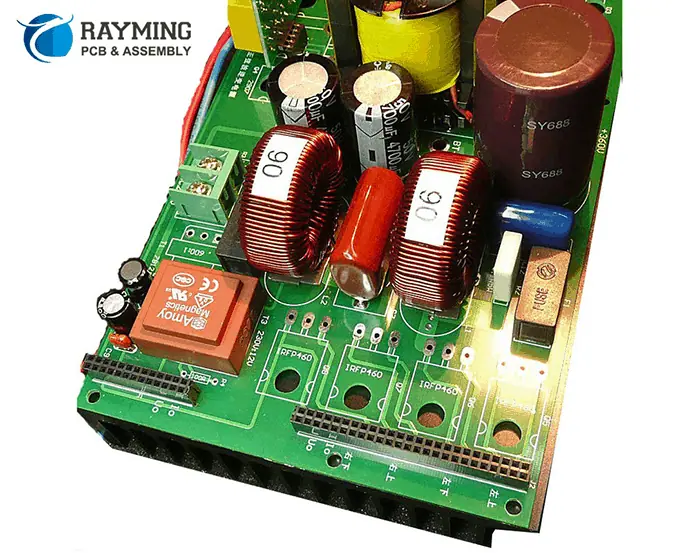
Incorporating Heat Sinks

Heat sinks are passive components that increase the surface area available for heat dissipation. They are typically made of materials with high thermal conductivity, such as aluminum or copper. To effectively use heat sinks:

  • Select heat sinks with appropriate fin designs for your space constraints
  • Use high-quality thermal interface materials to ensure good contact with hot components
  • Consider combining heat sinks with fans for enhanced cooling performance

2. Optimizing PCB Copper Usage

Copper plays a crucial role in heat dissipation within PCBs due to its excellent thermal conductivity. By strategically utilizing copper in your PCB design, you can significantly improve heat management.

Leveraging Thick Copper Traces

Increasing the thickness of copper traces can enhance their ability to conduct heat away from components. Consider the following when implementing thick copper traces:

  • Use wider traces for power and ground connections
  • Increase copper weight in areas with high heat generation
  • Balance trace thickness with manufacturing constraints and cost considerations

Implementing Copper Planes

Copper planes provide large areas for heat dissipation and can help distribute heat more evenly across the board. To effectively use copper planes:

  • Dedicate entire layers to power and ground planes when possible
  • Use thermal relief connections to prevent excessive heat sinking during soldering
  • Consider split planes to isolate noisy digital circuits from sensitive analog sections

Read more about:

3. Exploring Advanced Cooling Technologies

As PCB designs become more complex, advanced cooling technologies are being developed to meet the growing demands of heat dissipation.

Utilizing Heat Pipes

Heat pipes are sealed tubes containing a working fluid that efficiently transfers heat from one location to another. They can be particularly useful in designs where space is limited. When considering heat pipes:

  • Evaluate the orientation and length requirements for optimal performance
  • Choose appropriate working fluids based on your operating temperature range
  • Combine heat pipes with heat sinks or spreaders for enhanced cooling

Implementing Liquid Cooling Systems

For high-power applications, liquid cooling systems can offer superior heat dissipation compared to air-based methods. While more complex to implement, they can provide significant thermal management benefits:

  • Consider closed-loop systems for easier maintenance and reduced risk of leaks
  • Select appropriate coolants based on thermal properties and compatibility with materials
  • Design the system to minimize the risk of electrical shorts in case of leaks

Material Selection for Enhanced Thermal Management

The choice of materials used in PCB construction plays a critical role in heat dissipation. By selecting the right materials, you can significantly improve the thermal performance of your PCB design.

Substrate Materials: Balancing Performance and Cost

The substrate material forms the foundation of the PCB and greatly influences its thermal characteristics. Common options include:

  1. FR-4: Standard and cost-effective, but with limited thermal conductivity
  2. Aluminum PCBs: Excellent thermal conductivity, ideal for LED applications
  3. Ceramic substrates: High thermal conductivity, suitable for high-frequency applications
  4. Polyimide: Good for flexible PCBs with moderate thermal requirements

When selecting substrate materials, consider:

  • The thermal conductivity required for your application
  • Cost constraints and production volume
  • Electrical properties such as dielectric constant and loss tangent
  • Mechanical properties like flexibility and dimensional stability

Thermal Interface Materials: Bridging the Gap

Thermal interface materials (TIMs) are crucial for ensuring efficient heat transfer between components and heat sinks or other cooling solutions. Popular TIMs include:

  • Thermal greases
  • Phase change materials
  • Thermal pads
  • Thermally conductive adhesives

When choosing TIMs, consider factors such as:

  • Thermal conductivity
  • Ease of application and rework
  • Long-term stability and reliability
  • Compatibility with your assembly process

Powered By EmbedPress

Thermal Management Techniques for Compact PCB Designs

As electronic devices continue to shrink in size, managing heat dissipation in compact PCB designs becomes increasingly challenging. Here are some strategies to improve thermal performance in space-constrained designs:

Optimizing Component Placement

Careful component placement can significantly impact heat distribution across the board:

  • Group high-heat components together and place them near the board’s edges
  • Use thermal simulations to identify and address potential hot spots
  • Consider the impact of component placement on airflow patterns

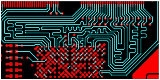
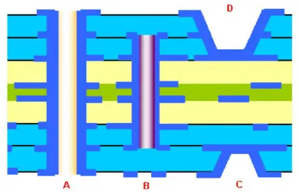
Leveraging Thermal Via Arrays

Thermal vias are plated through-holes that help conduct heat between PCB layers. To effectively use thermal via arrays:

  • Place them directly under or around hot components
  • Use a grid pattern to maximize heat transfer
  • Fill vias with thermally conductive materials for enhanced performance

Implementing Copper Coin Technology

Copper coins are thick pieces of copper inserted into the PCB to provide localized heat spreading. This technique can be particularly effective for managing heat from high-power components in compact designs:

  • Use copper coins under components with high thermal output
  • Ensure proper integration with the PCB manufacturing process
  • Consider combining copper coins with other cooling techniques for optimal results

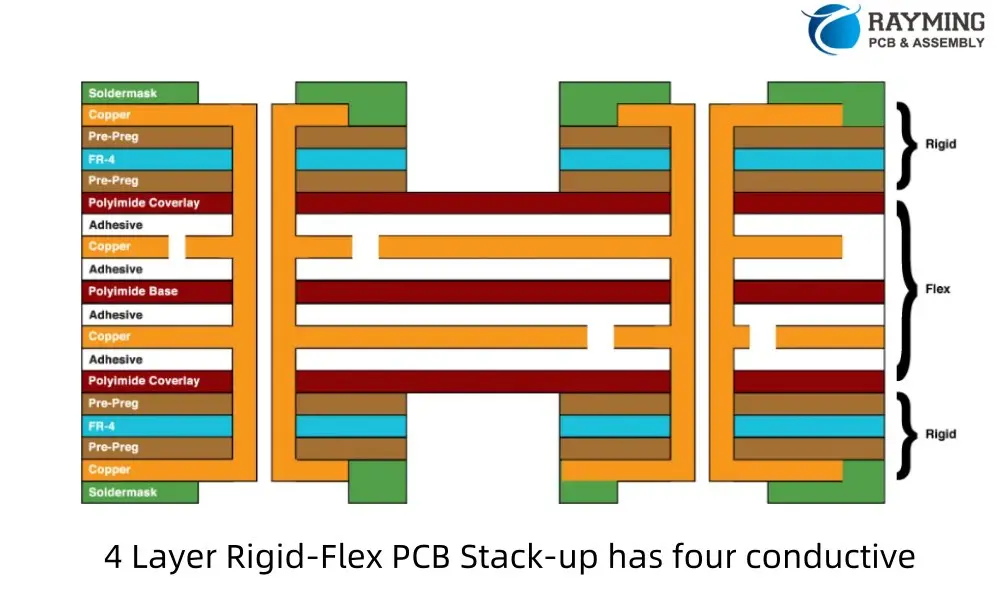
Heat Dissipation in Flexible PCB Designs

Flexible PCBs present unique challenges for heat dissipation due to their thin and bendable nature. However, several strategies can be employed to manage thermal issues in flex circuits:

Material Selection for Flex PCBs

Choose materials that balance flexibility with thermal performance:

  • Polyimide-based substrates offer good thermal stability
  • Consider hybrid designs with rigid sections for improved heat dissipation
  • Use thermally conductive adhesives for bonding layers

Implementing Copper Patterns

Strategic use of copper can enhance heat dissipation in flex circuits:

  • Utilize copper planes where possible, especially in areas with high heat generation
  • Consider hatched ground planes to maintain flexibility while improving thermal performance
  • Use thicker copper weights in critical areas, balancing thermal needs with flexibility requirements

Incorporating Thermal Management Layers

For applications with higher thermal demands, consider adding dedicated thermal management layers:

  • Integrate heat-spreading materials like graphite or aluminum
  • Use thermally conductive but electrically insulating materials to maintain signal integrity
  • Design thermal layers to work in conjunction with the circuit’s bending requirements

Conclusion: A Holistic Approach to PCB Heat Dissipation

Effective heat dissipation in PCB design requires a comprehensive approach that considers various factors, including:

  1. Component selection and placement
  2. Material choices for substrates and thermal interfaces
  3. Implementation of active and passive cooling solutions
  4. Optimization of copper usage and layout design
  5. Utilization of advanced thermal management techniques

By carefully considering these aspects and implementing appropriate strategies, designers can create PCBs that effectively manage heat, ensuring optimal performance and longevity of electronic devices. As technology continues to advance, staying informed about the latest developments in thermal management techniques and materials will be crucial for creating efficient and reliable PCB designs.

Remember, the key to successful heat dissipation in PCB design lies in finding the right balance between thermal performance, cost-effectiveness, and manufacturing feasibility. By adopting a holistic approach and leveraging the techniques discussed in this article, you can optimize your PCB designs for superior heat dissipation and overall performance.

What is the difference between a decoupling capacitor and a bypass capacitor?

Introduction

Decoupling and bypass capacitors are two of the most ubiquitous and important passive components used on printed circuit boards. They serve crucial functions in providing stable voltage regulation, filtering noise, and ensuring proper device operation.

While the terms “decoupling capacitor” and “bypass capacitor” are sometimes used interchangeably, there are in fact important distinctions between the two. Understanding the differences allows engineers to make informed design decisions when selecting and placing these capacitors.

This article provides an in-depth look at decoupling and bypass caps including:

  • The functions and purposes of each type
  • Key differences in behavior and characteristics
  • Guidelines for selecting the proper capacitance and type
  • Optimal placement considerations
  • Modeling and simulating decoupling performance
  • Mitigating decoupling issues like parallel and series resonance
  • Real-world decoupling design examples
  • Summary comparison of decoupling versus bypass caps

Read on to learn how proper utilization of decoupling and bypass capacitors can optimize circuit performance and prevent difficult-to-diagnose stability issues.

Functions of a Decoupling Capacitor

Decoupling capacitors, also known as bypass capacitors, serve several vital functions:

1. Maintain Steady Voltage to ICs

  • During operation, ICs can draw current in abrupt spikes and surges
  • This leads to fluctuations and noise on the DC power supply rails
  • Decoupling caps maintain a stable voltage by supplying current to the IC during demand spikes
  • They recharge quickly between spikes to remain ready for the next demand

2. Filter Noise

  • Switching noise is generated on power rails due to digital logic transitions
  • High frequency noise can impair circuit operation
  • Decoupling caps filter noise through low impedance across a wide frequency spectrum

3. Reduce Ground Bounce

  • Sudden current draw can cause ground potential to bounce or skew
  • Capacitors between ground pins dampen bounce and skew
  • This maintains signal integrity and noise margins

4. Control Impedances

  • Decoupling caps help control impedances along power distribution network
  • This avoids impedance discontinuities which reflect noise
  • Proper impedance helps signals propagate without distortion

In essence, decoupling capacitors act like small localized energy reservoirs to supply current, filter noise, and maintain stable voltage to enable proper functioning of nearby ICs and devices. Next, we’ll see how bypass capacitors serve some similar but also differing functions.

Functions of a Bypass Capacitor

While bypass capacitors provide some similar functions as decoupling caps, key differences include:

1. Differential Noise Rejection

  • Unlike decoupling caps directly from VDD to ground, bypass caps are placed in series from signal to ground
  • This attenuates common-mode noise while allowing the signal to pass
  • Useful for signals prone to picking up external interference

2. Band-Selective Filtering

  • Proper bypass cap selection targets filtering of specific noise frequencies
  • Values are chosen based on the frequency content to be rejected
  • Provides more selective filtering compared to broadband decoupling caps

3. Cross-Talk Reduction

  • In sensitive high-speed data links, capacitance between signal pairs reduces coupling
  • Prevents signals from influencing one another
  • Helps meet tighter timing margins at high data rates

4. Impedance Tuning

  • Unlike decoupling caps from VDD to ground, bypass caps are in series with signals
  • Can help fine tune characteristic impedance in transmission lines
  • Allows better impedance matching through the signal chain

In summary, while decoupling caps focus primarily on power integrity, bypass capacitors address signal integrity objectives. With the functions covered, let’s compare some key characteristics.

Key Characteristic Differences Between Decoupling and Bypass Caps

While there is some overlap in functions, several key characteristic differences help distinguish decoupling and bypass capacitors:

CharacteristicDecoupling CapacitorBypass Capacitor
LocationClose proximity between power and ground pinsIn series between signal and ground
PurposeMaintain steady voltage and filter power rail noiseAttenuate noise on signals and reduce cross-talk
CapacitanceHigh capacitance, small case sizesLower capacitance based on frequency response needs
PerformanceLow ESR and impedance over wide frequency rangeTargeted frequency response characteristics
TypesCeramic, polymer, tantalum, niobiumCeramic, film, mica, polystyrene
PackagingSurface mount chips, leaded disksSurface mount monolithic and stacked chips

Some key points:

  • Decoupling caps are placed close to IC power pins with short connections
  • Bypass caps are placed along signal paths, often near terminals
  • Decoupling caps need high capacitance in small sizes
  • Bypass caps focus on targeted frequency performance

Now let’s look at selecting appropriate capacitance values for the different applications.

Selecting Capacitance Value

The target capacitance value depends greatly on whether the capacitor will serve a decoupling or bypass function:

Decoupling Capacitors

  • Higher capacitance provides greater charge storage and noise filtering
  • Target mounting inductance limits useable capacitance
  • Typical sizes from 100nF to 10uF
  • 0.1uF, 0.47uF and 1uF most common

Bypass Capacitors

  • Chosen based on frequency response needed
  • Lower values for higher frequencies, higher for lower frequencies
  • 10nF to 100nF common for high speed serial links
  • 0.001uF to 0.1uF typical for operational amplifier power pins

Here are some guidelines for selecting decoupling capacitance:

1. Determine Charge Requirements

  • Estimate instantaneous charge needed during voltage spikes
  • Factors: chip size, power draw, activity level
  • More decoupling capacitance required for larger, more active ICs

2. Consider Distance to Power Supply

  • Further distance to power source requires more local charge reservoir
  • Increase decoupling caps for boards with single centralized regulator

3. Analyze Transient Loading

  • Circuits with larger instantaneous current spikes need bigger decoupling caps
  • Examine current draw waveform to determine worst-case transients

4. Factor in Inductance

  • Total inductance to capacitor limits high frequency performance
  • More capacitance can help compensate for higher inductance

With bypass capacitors, it is more important to select the proper capacitor technology for the desired frequency response. We’ll look more at passive component technologies later on.

Placement Considerations

Optimal placement is critical to maximize decoupling and bypass capacitor effectiveness.

Decoupling Capacitors

  • Place immediately adjacent to power pins to minimize loop inductance
  • Often locate multiple decoupling caps in parallel
  • Position between IC and next decoupling cap in the distribution network

Bypass Capacitors

  • Mount as close to the signal entry/exit point as possible
  • Minimize distance between bypass cap and signal plane
  • Place between signal source and noisy nodes

Some high performance PCB layout techniques include:

  • Embedded decoupling caps within the inner layers
  • Interdigitated capacitor arrays surrounding the IC
  • 3D capacitor stacks combining multiple height values
  • Periodic distribution of decoupling caps in grid patterns

Careful placement is key to realizing the full performance of both decoupling and bypass capacitors in the circuit.

Modeling and Simulating Decoupling

To analyze decoupling effectiveness, models are needed to simulate the PDN impedance behavior. Some approaches include:

IC Model

  • Simple model: Current source, resistor, and inductor
  • More complex: Resistor-capacitor (RC) network models IC and package
  • Determines current load used to stress the PDN

PDN Model

  • Capacitors, mounting inductance, plane impedance
  • Vias, power and ground planes, interconnects
  • Capture frequency-dependent impedance

Simulation Approaches

  • SPICE circuit simulations
  • Electromagnetic solvers for planes and components
  • Specialized PDN impedance solvers
  • IBM Power Delivery Network Analysis (PDNA) methodology

Simulations help predict resonances, identify insufficient decoupling, and determine impacts of board changes prior to a PCB layout. This enables proactive optimization of the decoupling network.

Mitigating PDN Impedances Issues

Decoupling capacitors help control PDN impedances, but potential issues must be addressed:

Parallel Resonance

  • Caused by capacitors and voltage plane inductance
  • Leads to unintended impedance peaks
  • Mitigate by reducing loop inductance and/or increasing capacitance

Series Resonance

  • Caused by capacitors and voltage plane capacitance
  • Causes unwanted impedance nulls
  • Mitigate by reducing plane capacitance and/or inductance

Spreading Inductance

  • Currents spread non-uniformly in planes causing varying inductance
  • Manage by proper decoupling placement, via distribution, and ground pours

Insufficient Decoupling

  • Too little capacitance fails to supply transient current loads
  • Add more decoupling caps near problem area
  • Increase capacitance and reduce mounting inductance

Thorough PDN planning, simulation, and design reviews help identify and resolve decoupling issues before manufacturing the PCB.

Real-World Decoupling Capacitor Design Examples

Here are some examples highlighting decoupling design and optimization for different applications:

1. High-Speed Memory Interface

  • DDR5 interface with memory controller IC
  • High transient currents and noise at >5GHz speeds
  • Target impedance below 0.5 ohm up to 5GHz
  • Employed Pi-filter decoupling with two parallel 100nF MLCC caps and ferrite bead
  • Used interdigitated capacitors adjacent to IC with ground vias in grid pattern

2. Automotive RADAR PCB

  • 24 GHz MMIC (monolithic microwave IC) RF transceiver
  • Extremely low supply noise required for phase coherence
  • Leveraged embedded distributed capacitance below ICs
  • Surrounded MMIC with multi-density stack of capacitors: 4x10nF, 2x100nF, 10uF tantalum
  • Extensive power plane copper fills to reduce spreading inductance

3. High Power GPU

  • High current transient loads up to 150A
  • Target impedance below 5mohm up to 100MHz
  • Employed land-side capacitors with bottom-side ground vias
  • Grid of 4x1000uF POSCAP tantalum bulk capacitors
  • 20x10uF ceramic capacitors distributed around processor

These examples showcase real-world applications of effective decoupling design techniques tailored to the specific requirements.

Comparison Summary: Decoupling vs. Bypass Capacitors

Here is a summary overview of the key differences between decoupling and bypass capacitors:

ParameterDecoupling CapacitorBypass Capacitor
LocationNear IC power pinsAlong signal path
PurposeStable voltage, filter noiseAttenuate signal interference
Capacitance ValueHigher, depends on IC current demandLower, based on frequency response
PerformanceLow impedance over wide frequency bandTargeted filtering for noise frequencies
TypesCeramic, polymer, electrolyticCeramic, film, mica
PackagingSurface mount, through-holeMonolithic and stacked surface mount
ResonancesMitigate parallel and series resonanceLess susceptible
ModelingPDN impedance, IC transient loadsSource and load termination

This summarizes some of the key differences in a concise comparison table. Both capacitor types are critical PCB components but address distinct requirements.

Frequently Asked Questions

Here are some common FAQs regarding decoupling and bypass capacitors:

Q: Can a bypass capacitor be used for decoupling and vice versa?

In some cases yes, but performance may be compromised compared to using the optimal type. The distinguishing factors are location relative to power vs. signal pins and wide-band vs. selective frequency response characteristics.

Q: How are bypass/decoupling capacitors modeled in circuit simulation?

Decoupling caps are modeled as part of the full PDN with emphasis on equivalent series inductance. Bypass caps can be modeled as simple capacitive sources with appropriate frequency-dependent impedance characteristics.

Q: What testing is done to characterize decoupling capacitor performance?

Parameters like equivalent series resistance/inductance and impedance versus frequency may be tested to characterize decoupling effectiveness across operating frequency ranges.

Q: How can I calculate the target impedance for my PDN?

Factors like anticipated load transient current, switching noise tolerance, and voltage margin are used to estimate the maximum allowable PDN impedance based on voltage deviation limits.

Q: What construction techniques help reduce inductance?

Shorter traces, interdigitated capacitors, embedded capacitance, and vias in tight grid patterns all help minimize mounting loop inductance.

Conclusion

Decoupling and bypass capacitors address unique but equally vital functions in maintaining proper circuit operation. As PCBs continue advancing to faster speeds and lower voltages, utilizing the appropriate capacitor technologies and design techniques is imperative. Understanding the key distinctions between decoupling and bypass caps will enable engineers to make informed design decisions.

The detailed comparisons and examples in this article equip PCB designers with deep knowledge to deploy decoupling and bypass capacitors effectively. By leveraging the right capacitor solutions tailored to each application’s specific needs, robust performance and stability can be achieved.

What Circuits are Used to Generate Clock Signals?

Introduction

Clock signals are essential timing references used to synchronize and coordinate the operation of digital logic circuits in integrated circuits and electronics systems. A clock waveform oscillates between a high and low logic level at a regular frequency. The transition edges trigger sequential logic state changes and digital computations. Clock signals must exhibit precise frequencies with low jitter and high spectral purity for reliable circuit operation.

Various clock generation circuits are available to produce different frequencies using crystal, relaxation, ring, and phase-locked loop oscillators along with frequency multipliers and dividers. Selecting the right approach depends on frequency stability, jitter, power and tuning range requirements. This article provides an overview of commonly used clock generation circuits highlighting their operating principles, characteristics, and applications.

Clock Signal Properties

Classic Circuit Analysis--Clock Circuit
Classic Circuit Analysis–Clock Circuit

Desirable attributes of stable clock signals are:

  • Accurate oscillation frequency matching system specifications
  • Low cycle-to-cycle jitter to precisely trigger logic
  • High spectral purity with minimal harmonics
  • Square waveform with fast rise and fall times
  • Constant peak-to-peak voltage amplitude
  • Low duty cycle distortion
  • High signal integrity over chip/board distribution

Crystal Oscillator

This uses the mechanical resonance of a vibrating crystal to generate a sinusoidal signal at a precise natural frequency determined by the crystal cut and dimensions. Feedback amplifiers sustain the oscillations applying bias voltages and limiting gain to overcome losses. Output buffers provide squared CMOS/TTL compatible clock outputs.

Characteristics

  • Excellent frequency stability and accuracy
  • Low jitter (<100 ps)
  • High spectral purity
  • Frequency range from kHz to MHz

Applications

  • Primary system reference clocks
  • Real-time clocks
  • RF systems
  • Instrumentation

Relaxation Oscillator

Here an RC network is repetitively charged and discharged between two voltage thresholds to produce a timing clock signal. Comparators switch the output state when the RC voltage crosses the thresholds.

Characteristics

  • No external components
  • Moderate accuracy and stability
  • Higher jitter
  • High power consumption

Applications

  • Embedded microcontroller clocks
  • Timer circuits
  • Low-frequency clock generation

Ring Oscillator

This consists of an odd number of inverting logic gates connected in a circular chain. The output of the last gate is fed back to the input of the first, causing oscillations at a frequency determined by the gate delays. Buffers provide synchronized outputs.

Characteristics

  • Completely on-chip integration
  • Tunable frequency by control voltage
  • Moderate jitter
  • Noisy output requiring filtering

Applications

  • On-chip clock generation
  • Analog-to-digital converters
  • Frequency synthesis in PLLs
  • Random number generation

Phase Locked Loop (PLL)

Classic Circuit Analysis--Clock Circuit
Classic Circuit Analysis–Clock Circuit

A PLL synchronizes its oscillator output to match either an external reference clock or crystal oscillator using a feedback control loop. The phase detector generates error voltages proportional to phase differences driving the oscillator frequency toward zero phase error.

Characteristics

  • Excellent frequency stability when locked
  • Very low jitter

-Tunable frequency multiplication/division

  • Integrated implementations

Applications

  • Microprocessor/communication IC clocks
  • Frequency synthesis of various clock rates
  • Clock recovery from data communications
  • Frequency modulation/demodulation

Clock Conditioning Circuits

Supplementary circuits help provide final clock signals with desired characteristics:

Frequency Multipliers

Use analog or digital techniques to generate harmonic multiples of an input reference frequency. Popular for sub-clock generation.

Dividers

Divide input clock frequencies down digitally to lower clock rates using ripple counters or synchronous counters.

Buffers

Provide periodic clock signal refreshment, fanning-out, and amplitude limiting to safely drive large clock distribution loads.

Filters

Remove noise and harmonics to improve spectral purity using LC and RC low-pass filters.

Clock Distribution

The generated clock is distributed to various logic blocks using balanced trees and grid networks overlaid on chip or board along with careful impedance control, termination and buffering to control reflections and skew.

Choosing Clock Generation Circuits

The table below summarizes the key selection criteria:

ParameterCrystal OscillatorRC OscillatorRing OscillatorPLL
Frequency StabilityExcellentPoorModerateExcellent (with reference)
Frequency TunabilityFixedLimitedExcellentExcellent
JitterVery lowHighModerateVery low
Spectral PurityExcellentModeratePoor (spurs)Excellent
Integration LevelExternalMediumHighHigh
Power ConsumptionLowHighMediumMedium

Conclusion

A wide variety of clock generation circuits provide multiple options to engineers designing digital systems, based on requirements like operating frequency, jitter tolerance, tunability, cost and power constraints. Proper selection coupled with robust distribution network design delivers stable synchronized timing signals vital for reliable functioning of synchronous logic circuits. Given their criticality, clocking circuits and techniques continue to be an area of innovation to support advancing chip technologies and faster computing systems.

Frequently Asked Questions (FQA)

Q1: Why is using a crystal oscillator better than an LC tank oscillator for clock generation?

A1: The precise resonant frequency of quartz crystals gives extremely stable and accurate clock signals in comparison to LC tank circuits which are susceptible to drift with temperature and component variations.

Q2: What techniques can be used to reduce clock jitter from oscillators?

A2: Using higher Q-factor crystals/LC tanks, providing sufficient loop gain in oscillator feedback paths, maintaining well-regulated bias voltages, filtering noise sources, and buffering clock signals before distribution help minimize jitter.

Q3: How does a phase-locked loop provide tunable clock generation?

A3: The voltage-controlled oscillator inside the PLL allows its output clock frequency to be tuned across a range determined by the VCO transfer characteristic. The PLL locks the VCO to an accurate reference input clock.

Q4: Why is clock signal integrity important in digital systems?

A4: Clean clocks with balanced rise/fall times, constant amplitude and shape are critical for synchronous digital logic. Noise, reflections, jitter degrade switching performance and computation reliability.

Q5: How can multiple clock frequencies be generated from a single reference source?

A5: Using a frequency divider produces integer sub-multiples of the source frequency. Frequency multipliers and mixers generate harmonic multiples. PLLs allow both integer scaling and arbitrary frequency synthesis.

What is the opening shave for soldermask?

Introduction

Soldermask or solder resist is the protective layer of polymer coating applied over the copper traces on printed circuit boards (PCBs) to control solder spreading and prevent bridging between pads during component assembly. Openings in the soldermask selectively expose the underlying copper pads that need soldered connections. The width of these openings relative to the pad size is known as the opening shave.

This article provides a detailed overview of soldermask opening shave including its purpose, typical values, how it is designed, considerations for different pad shapes, and effects on manufacturability and soldering defects. Guidelines are provided for calculating appropriate opening shave widths based on pad geometries and solder flow needs.

Purpose of Opening Shave

The main objectives of providing additional open area around pads include:

  • Exposes the surface of pad for sufficient solder wetting.
  • Accommodates registration tolerances of soldermask alignment.
  • Allows a channel for outflow of excess solder away from the pad.
  • Improves manufacturability by reducing probability of mask openings shrinking smaller than pads.
  • Lowers risks of solder bridging between neighboring pads.

Typical Opening Shave Values

Industry standard IPC-7351 specifies a minimum annular ring of 3 mils (75 μm) of open pad area extending beyond the soldermask on all sides. However, common design values are:

  • Low density through-hole pads: 5 to 8 mils
  • High density surface mount pads: 4 to 6 mils
  • Fine pitch components: 3 to 4 mils

Higher opening shaves up to 10 mils may be used in vibration environments where soldermask separation risks are higher.

Design Factors for Opening Shave

Key considerations while designing opening shave include:

  • Registration tolerance between pads and soldermask image
  • Pad shape and orientation – square pads need larger shave
  • Pad density – higher density needs tighter shave to avoid bridging
  • Soldermask expansion space from pad for outflow
  • Copper pad thickness – thicker copper allows slightly smaller shave
  • Soldermask material – photoimageable masks hold registration better
  • Vibration levels – shave increased at vibration prone regions
  • Rework considerations – sufficient space for rework and solder cleanup

Opening Shave for Different Pad Shapes

Rectangular Pads

A symmetrical shave of 4-6 mils on all sides is typical. The long edge shave may be 1 mil higher if length exceeds 1.5 times width.

Square Pads

Require at least 4 mils additional opening on all four sides due to higher bridging risks along diagonals.

Rounded Pads

Here adjusted shave widths compensate for shorter distance along curved edges:

Rounded pad soldermask opening (Image Credit: PCB Square)

Effects of Inadequate Opening Shave

Insufficient shave exposing the pad can lead to:

  • Dry solder joints or incomplete wetting if mask overlaps pad area
  • Solder masking separation under thermal stresses, closing the designed openings
  • Solder spread into narrow openings increasing bridging tendency
  • Voids and trapped fluxes due to lack of outflow clearance
  • Inability to clean undermask areas during rework

Solder Defects Related to Opening Shave

Various soldering defects can be caused or exacerbated by improper control of soldermask opening shave:

Solder Bridging

Pulling in of solder between adjacent pads when clearance space is inadequate.

Solder Balling

Fluid solder gathering into spheres instead of wetting pad surfaces when openings are mismatched.

PCB Delamination

Soldermask separation from pad edges under vibration or thermal stresses exposes more copper area.

Solder Beading

Ring-shaped solder bead formation along pad periphery when mask overlaps pad.

Solder Mask Slivers

Sliver-like leftovers of soldermask inside openings interfering with wetting.

Guidelines for Calculating Opening Shave

1. Determine pad size and shape

  • Measure length, width for rectangular pads
  • Define diameter for rounded pads

2. Account for soldermask registration tolerance

  • Typically around 4 mils (100 μm)

3. Add minimum annular ring width

  • IPC-7351 recommends 3 mils (75 μm)

4. Provide expansion clearance

  • 2 mils for most pads
  • 4 mils for large pads > 40 mil sides

5. Round shave dimensions up to nearest 0.5 or 1 mil grid

  • Simplifies manufacturing tolerances

6. Increase shave for vibration exposure

  • Add 2-4 mils for vibration prone regions

7. Verify shave against IPC or manufacturer’s guidelines

  • Reshape pad if needed to allocate sufficient shave

Conclusion

The soldermask opening shave is a small but vital PCB design parameter that prevents defects and rework in assembly by properly exposing pads for clean soldering while limiting bridging risks. Applying appropriate shave margins based on pad sizes, shapes and density allows high soldering yield. As PCB fabrication precision improves, opening shaves continue to shrink permitting further miniaturization.

Frequently Asked Questions (FQA)

solder mask
solder mask

Q1: How is the registration tolerance between pads and soldermask openings reduced?

A1: Using photosensitive soldermasks exposed with the same PCB pad image minimizes image translation errors. Laser direct imaging can further improve alignment precision.

Q2: Which pad shape typically requires largest opening shave?

A2: Square pads need relatively larger shave margins along the pad diagonals to avoid bridging compared to rectangular pads. Rounded pads allow tightest shave due to reduced meniscus formation along curved edges.

Q3: How does soldermask thickness impact the opening shave?

A3: Thicker masks impart greater stress on pads risking delamination and separation. This may necessitate slightly higher shave values. Typical mask thickness is around 3-5 mils.

Q4: When is a larger than normal opening shave warranted?

A4: In vibration prone environments, where differential expansion might gradually expose more pad area. Also, where anticipation of numerous rework cycles requires extra clearance for cleaning undermasks.

Q5: How is opening shave optimized for fine pitch components?

A5: Reducing shave close to the minimum recommended values allows tighter packing while preventing bridging between adjoining pads. This requires high precision imaging and registration process capabilities.

How to design pcb soldermask opening

This article mainly introduces the opening of pcb. Firstly, it introduces opening and bright copper in PCB design. Secondly, it introduces how to realize the tinning of PCB wiring. Finally, it explains the steps of how to set the opeining.

What is the pcb soldermask opening?

The circuit on the PCB are covered with soldermask to prevent short circuits and damage the device. The so-called solder mask opening is to remove the paint layer on the circuit, so that the circuit can be exposed to tin.

gold pcb pad

As shown in the above picture, it is the opening. PCB opening is not uncommon. The most common one is probably the memory stick. The students who have removed the computer know that the memory stick has a gold finger, as shown below:

gold finger

The golden finger here is to opeing, plug and play.

There is also a very common function of opening the opening, which is to increase the thickness of the copper foil in the later period, which is convenient for excessive current, which is more common in the power board and the motor control board.

opening and bright copper in PCB design

In the design, customers often ask for opening and bright copper. Because the customer is also ignorant or we are not too clear about this process, it is very troublesome to communicate. In our design, we often encounter customers who need to add shields, partial bright copper on the board side, through-hole open-resistance soldering, copper on the back side of the IC heat sink, and scratch pad. According to the actual situation, let’s take a look at several sets of pictures to explain.

1, shield

If the customer needs to add a shield, then all we have to do is add a Soldmask with a width of at least 1mm. If you need to add a stencil, you need to confirm with the customer. At the same time as adding the Soldmask, we need to spread the network copper in the add mask area, and we must cover the Soldmask plane, otherwise the pcb substrate (FR4, etc.) will be exposed. Other non-local networks should not pass through the Soldmask. Adding a loosemask area to the pcb effect reveals a yellow copper. Solder mask coverage is provided for areas that are not added.

IC gold pad

2, solder mask opening hole

In the design, we often hear the whole plate plug hole or partial plug hole. When adding the hole, we pay attention to the fact that the plug hole company name generally refuels the BGA, and vice versa. ). In general, a company that has a specification of more than 12 mils must use a solder mask opening.

pcb layout

3, IC thermal pad

Generally, a solder-proof PAD is added on the back of the IC heat-dissipation pad (adding a shoulder mask larger than the surface layer or equal to the surface of the surface pad) and a ground hole, and a copper-clad solder mask is placed on the back surface to better pass the heat of the surface layer. The hole in the hole is transmitted to the back of the copper skin to disperse better.

pcb layout

4,The Pad tin touched

In wave soldering, in order to solve the problem of tin bonding caused by the tight pitch of the pads, we will use the shape of the scratch pad. Note that it is necessary to add copper bumps of the same size as the solder mask while adding the solder mask.

pcb Pad

How to realize PCB trace opening

In the circuit vias, it is necessary to drive 8 relays. When the multi-channel relays are turned on, the current is greatly increased. To ensure the actual effect, while widening the current line, it is desirable to remove the solder mask on the current – the green oil layer, and the board is made. In the future, you can add tin to the top, thicken the line, and pass more current.

The actual results are as follows:

pcb circuit line

The implementation method is as follows:

Draw this line in the layer of the top PCB layer (or bottom layer depends on the layer where the preset line is located), and then draw the line that coincides with this in the top solder (or bottom solder) layer.

How to set the circuit to open

The PCB design can be used to set the opening on the TOP/BOTTOM SOLDER layer.

TOP/BOTTOM SOLDER (top/bottom solder mask green oil layer): The top/bottom layer is coated with solder resist green oil to prevent tin on the copper foil and keep it insulated.

A solder resist green soldermask opening can be placed on the pads, vias, and non-electric traces of this layer.

  1. The pad will open by default in the PCB design (OVERRIDE: 0.1016mm), that is, the pad exposed copper foil, the outer expansion is 0.1016mm, and the wave soldering will be tinned. It is recommended not to make design changes to ensure solderability;

2, the via hole in the PCB design will open by default (OVERRIDE: 0.1016mm), that is, the through hole exposed copper foil, the external expansion 0.1016mm, the wave soldering will be tin. If it is designed to prevent tinning on the vias and do not expose copper, you must tick the PENTING option in the additional properties of the vias SOLDER MASK to close the vias.

  1. In addition, this layer can also be used for non-electrical routing, and the green soldering resistance should be opened accordingly. If it is on the copper foil trace, it is used to enhance the overcurrent capability of the trace. When soldering, it can be tinned. If it is on the non-copper foil trace, it is generally designed for marking and special character silk screen, which can save production. Character silkscreen.

How Do You Design a Power Supply?

power pcb

Introduction

A power supply is a crucial component that converts power from a source to the regulated voltages required by electronic circuits and systems. The proliferation of electronic devices has led to power supplies being ubiquitous, ranging from chargers for mobile phones to high capacity supplies in data centers. Designing a proper power supply requires expertise in multiple engineering domains encompassing power electronics, analog design, control theory, and thermal management.

This article provides a step-by-step guide on designing a power supply covering aspects like topology selection, power stage design, feedback and control, safety standards compliance, thermal design, and electromagnetic compatibility. By following the structured design methodology, electrical engineers can develop reliable and efficient power supplies tailored to their application needs.

Functional Requirements

Switching Power Supply Design

Defining the right specifications and functional requirements is the critical first step that sets the overall direction for the power supply design.

Input Voltage Range

The expected input voltage range should be specified, including minimum, nominal, and maximum voltages. Common input ranges are 5V, 12V, 24V, or 48VDC derived from rectified mains AC or batteries. Wider input ranges require designs that can maintain regulation over the span.

Output Voltages and Currents

The desired output voltages and load currents should be specified. For multiple outputs, cross-load dependencies and sequencing needs must also be considered. Safe margins above nominal loads should be included for fault conditions. Prioritizing critical outputs helps allocate design resources effectively.

Efficiency Targets

Required full load and partial load efficiencies at nominal voltages determine components selection and loss budgeting. Light load efficiency is also critical for new energy-efficiency standards.

Power Density Targets

The desired power density (watts/cubic inches) influences how compactly the design must be packaged. It requires trade-offs with efficiency and thermal performance.

Safety and Emissions Compliance

Regulatory standards like medical and IT equipment safety, conducted emissions, and radiated emissions compliance must be considered.

Reliability Requirements

Requirements like MTBF, expected service life, and environmental survival ranges help guide design choices for component deratings and redundancies.

Control Characteristics

Needs like remote control, sequencing, telemetry, and margining control influence digital control and communication features.

Topology Selection

The choice of power conversion topology sets the foundation for meeting the design goals. Different topologies have inherent advantages and limitations.

Linear Regulator

A linear regulator maintains output voltage by dropping excess input voltage across a series pass element. The advantages are simplicity, low noise, and fast response. But poor efficiency at lower output voltages makes them unsuitable for high power applications.

Switching Regulator

Switching converters use semiconductor switches to transfer chunks of energy to the output in a controlled pulsed manner. Switching loss is lower than a linear regulator, allowing high efficiency conversion even for large voltage drops. However, switching noise requires careful filtering.

Various sub-classes of switching regulators offer further topological choices:

  • Buck Converters: Used for step-down conversion from higher input to lower output voltage.
  • Boost Converters: Used for step-up conversion from lower input to higher output voltage.
  • Buck-Boost Converters: Allows both step-down and step-up conversion flexibly.
  • Isolated Topologies: Flyback, forward, push-pull, and full-bridge converters use transformers for isolation and multiple outputs.

Selection criteria include required conversion ratio, complexity, component stresses, efficiency, and isolation needs.

Resonant and Soft-Switching Topologies

Resonant converters and quasi-resonant soft-switching schemes reduce switching losses allowing very high efficiency conversion. However, the added complexity may not justify gains for lower power applications.

Power Stage Design

pcb-power-supply

The power stage handles the actual power conversion between input and output. It consists of elements like switches, diodes, inductors, transformers, and capacitors.

Semiconductor Switch Selection

MOSFETs and IGBTs are suitable semiconductor switch choices for power supplies below 500W. High current capability MOSFETs allow simpler synchronous rectifier buck designs. Above 500W, IGBTs tend to be more robust. Availability of integrated power modules with paralleled devices simplifies high current designs.

Passive Components

  • Inductors: Value selection involves tradeoffs between ripple, response time, and component size. Core materials and shapes like toroids or pot cores optimize efficiency.
  • Transformers: Core geometry, materials, gap design, winding techniques, and layered or interleaved windings affect performance.
  • Capacitors: A mix of electrolytic and multilayer ceramic capacitors provides bulk capacitance and high frequency bypassing.

Snubbers and Clamps

Snubbers like RC networks suppress voltage spikes across switches during switching transitions. Clamps help limit overvoltage events.

Layout and Parasitics

Careful component placement and routing minimizes the length of high current paths to reduce parasitic inductance and resistance. Separating noisy switching nodes from sensitive analog areas is necessary.

Feedback and Control

To maintain stable regulated output voltages, feedback control forms a closed loop system adjusting PWM switching patterns based on output voltage deviations from the reference.

Voltage Dividers

Properly designed resistive divider networks scale output voltages to levels acceptable for the feedback IC. Filtering may be required for noise reduction.

Feedback IC

Specialist ICs provide operational amplifier, pulse width modulation (PWM), compensation circuits and protection features needed for robust control and regulation of switching converters.

Compensation Network

This provides the corrective feedback and stability for the control loop. The network sets gain crossover and phase margin by shaping the IC loop gain to target stable response with adequate noise immunity.

Digital Control

Incorporates monitoring, diagnostics, communication, and adaptive tuning functions via a microcontroller. This allows sophisticated control algorithms and remote user interfaces.

Protection Features

Protection safeguards the power supply and connected load during abnormal conditions. Common protections include:

  • Overvoltage protection – Shuts down supply if output exceeds preset safe threshold.
  • Undervoltage protection – Shuts down supply if output sags excessively under minimum level.
  • Overcurrent protection – Shuts down supply if load current exceeds set limit indicating a short circuit.
  • Over temperature protection – Shuts down supply if internal temperatures rise beyond safe operating limit.
  • Input under/over voltage lockout – Disables output if input is outside operating range.
  • Redundancy – Secondary backup units takeover upon failure detection
  • Surge and transient protection – MOVs, RC snubbers absorb incoming surges on input.

Thermal Design

Generating substantial heat is an inherent consequence of power conversion. Effective thermal management is vital for reliable operation and safety.

Power Dissipation Analysis

The distribution of losses in switches, magnetics, and other components determines cooling requirements. Analytically derived and validated through simulations.

Heatsink Design

Heatsinks provide convective cooling matched to the power dissipation profile. Fin geometry, airflow passage design, heat pipe augmentation, and interface materials influence heatsink performance.

Airflow and Ventilation

Fans and airflow ducting maintain sufficient directed airflow through heatsinks and the housing. Intake and exhaust vents are designed to utilize natural convection also.

Thermal Interface Materials (TIMs)

TIMs like thermal pads, greases, or phase-change compounds improve heat conduction from components to heatsinks.

EMI/EMC Design

High Power PCB Design

Switching power supplies generate significant high-frequency noise requiring careful mitigation to meet EMI limits and prevent conducted/radiated interference with other devices.

Input Filtering

Pi-filters and ferrite beads supress current-driven differential mode noise propagating from the AC input to the power stage.

Output Filtering

Capacitors, ferrites, and LC filters clean up switched-mode noise in DC output to avoid contaminating sensitive downstream circuits. Shielding on cables also reduces emissions.

Circuit Partitioning

Keeping noisy power circuits physically separate from analog and digital control areas through partitioning, shielding and isolation helps reduce interference coupling.

EMI Reduction Techniques

Spread spectrum frequency modulation, soft-switching, snubbers, and proper grounding and shielding all help minimize emissions at source.

Shielding

Proper enclosure shielding and correct filter feedthrough component installation is critical to contain radiated emissions. PCB stitching vias help shield leakage from gaps in ground planes.

Physical Design and Packaging

The physical design and packaging determines the integrity and usability of the power supply.

Enclosure and Chassis

The enclosure provides mechanical support, safety isolation between circuits and users, shielding for EMI control, and channels airflow for ventilation.

PCB Layout

PCB component placement and routing optimizes current flows, minimizes parasitics, provides noise isolation between stages, and facilitates servicing and manufacturability.

Cables, Connectors, Indicators

Cabling connects internal electronics to external interfaces like the AC inlet, DC output terminals, and control connectors reliably. Indicator lamps display enabled/fault statuses.

Environmental Protection

Conformal coatings protect against dust, moisture, and temperature extremes. Potted enclosures improve vibration and shock survivability.

Compliance Testing and Certifications

Verification testing ensures the design meets requirements and passes mandatory certifications for the target application and market.

Functional Testing

Confirm basic functionality across operating conditions of loads, voltages, temperatures, and frequencies. Burn-in reliability testing stresses components.

Safety Standards

Certifications like UL, CSA, ENEC for end-use product safety requirements including insulation, fault tolerance, construction, marking.

EMI and EMC

Testing for conducted and radiated emissions, immunity to interference, and surge withstand verifies compliance to FCC, CE standards.

Environmental Tests

Verifies operation under challenging environmental stresses like temperature, humidity, vibration, shock, salt-fog, and ingress protection.

Conclusion

Designing reliable, efficient, and fully-featured power supplies requires expertise across multiple engineering domains coupled with practical experience guiding design choices. A structured approach allows methodically addressing requirements and making sound trade-offs from topology selection to packaging. Utilizing rigorous compliance testing ensures regulatory and safety standards are satisfied before product release. The demand for well-designed cost-effective power supplies will only grow given their ubiquitous role in powering modern technological advances.

Frequently Asked Questions (FQA)

Q1: What is the difference between linear and switch mode power supplies?

A1: Linear power supplies regulate output voltage by dropping excess input voltage across a pass element, allowing continuous output current but with poor efficiency at lower output levels. Switch mode supplies chop input voltage into pulses using semiconductor switches, converting it more efficiently through an inductor into lower average output voltage.

Q2: How do you ensure stable voltage control in switch mode power supplies?

A2: A negative feedback control loop compares actual output voltage against a precision reference using an error amplifier. The loop compensates by increasing or decreasing the duty cycle of the PWM switched input to maintain the required output voltage irrespective of changing load conditions.

Q3: What protections should be incorporated in a well-designed power supply?

A3: Protections for over-voltage, under-voltage, over-current, over-temperature, input voltage out-of-range conditions should be implemented. These detect fault conditions and safely shut down or restart the power supply as appropriate. Redundant operation can also provide backup protection.

Q4: What construction techniques help reduce EMI from power supplies?

A4: Shielding the power supply enclosure, minimizing gaps in return paths, keeping noisy circuits physically separate from sensitive ones, using appropriate input and output filters, PCB partitioning, as well as spread spectrum and soft-switching techniques reduce emitted and conducted EMI.

Q5: What are some important regulatory approvals and certifications for power supplies?

A5: Safety certifications like UL, CSA, ENEC, CE are mandatory for commercial power supplies. FCC, CISPR compliance is required for radiated and conducted emissions. Specialized medical and industrial equipment certifications may also be required depending on the application.

What is High Density PCB?

High-Speed High-Density PCB

Introduction

Printed circuit boards (PCBs) form the backbone of all electronic devices providing the platform to mount components and interconnect them. With rapid technological advancements and need for product miniaturization, PCBs have become increasingly complex and crowded. This had led to the growth of high density interconnect (HDI) PCB technology to provide the wiring density needed by advanced electronics.

High density PCBs allow packing of high component densities and fine features into smaller board areas. They enable integration of more functionality into compact and lightweight electronics. HDI capabilities are critical for products like smartphones, wearables, IoT devices, medical equipment etc. that require maximum hardware capabilities within tight space constraints.

This article will provide an in-depth understanding of what constitutes a high density PCB, the key technologies enabling HDI boards and their applications.

What Makes a PCB High Density?

qrf

A high density PCB can be defined as a board with:

  • Fine trace/space width ≤ 100 μm (4 mils)
  • High layer count ≥ 6 layers
  • Blind and buried vias for routing between inner layers
  • Microvias with diameters ≤ 150 μm, typically 50 to 80 μm
  • High component density with pad/pitch ≤ 0.4 mm

To achieve these high wiring densities, HDI PCBs leverage technologies like laser drilling and imaging of fine features, thinner dielectrics, sequential lamination, and more.

Some key characteristics of HDI boards from standard PCBs are:

FeatureStandard PCBHDI PCB
Line/Space≥ 125 μm≤ 100 μm
Via diameter≥ 150 μm≤ 80 μm
Via pad size≥ 350 μm≤ 250 μm
Layer count≤ 12≥ 6, up to 30+
Dielectric thickness≥ 50 μm≤ 40 μm
Solder maskLiquid photoimageableLaser direct imaging
Finished thickness1.6 mm≤ 1.0 mm

Evolution of High Density Interconnect Technology

The origins of HDI technology can be traced back to the 1980s when traditional PCB fabrication techniques started reaching their limits as circuit densities grew. Some key milestones in the development of HDI are:

  • Mid 1980s – Surface mount technology and multilayer boards started gaining adoption to support denser packaging and routing.
  • Late 1980s – Microvia technology was developed by IBM allowing connections between layers with small vias. This avoided the need to route lines all the way to the outer layers.
  • Early 1990s – Build up layer (BUL) process introduced by Intel-Microsoft consortium to build additional thin signal layers on top of a core board.
  • Mid 1990s – Laser direct imaging adopted for fine photolithography to create traces below 25 μm.
  • Early 2000s – Stacked microvias and sequential lamination refined the basic HDI processes.
  • 2010s – With growth of smartphones, HDI became ubiquitous globally. Lines/spaces dropped below 20 μm.

Continued innovation in materials and processes has enhanced the capabilities of HDI technology to keep pace with market requirements.

Key Technologies Enabling High Density PCBs

A number of advanced PCB fabrication technologies are essential to manufacture the high density boards needed today:

Laser Drilling

Mechanical drilling cannot achieve the 5 mil and lower via sizes seen in HDI. UV lasers are used drill these miniscule vias with high accuracy at tight pitches. Laser also produces cleaner via walls and avoids issues like smear and epoxy clogging faced with small bits.

Thin Dielectrics

Standard glass fabric substrates are too lossy and thick for high speed HDI boards. Teijin’s Nexus and Panasonic’s Megtron 6 are popular low-loss thermoset laminates with dielectric thicknesses down to 25 μm. These allow tighter lines/spaces and prevent signal integrity issues.

Direct Imaging

To fabricate ultra-fine traces below 25 microns, photolithographic methods are used instead of mechanical print-and-etch process. Liquid photoresists are exposed using laser direct imaging to define the circuit patterns with high precision.

Blind and Buried Vias

Blind/buried vias are drilled and plated before lamination of the outer layers, allowing connections between inner layers without consuming routing space. This provides tremendous routing flexibility in HDI designs.

Microvias

These are small vias with diameters typically between 50 to 80 μm drilled with lasers. Microvias connect adjacent layers in HDI boards without using board area.

Build Up Layers

Additional thin dielectric layers are added on either side of the core HDI board using sequential lamination. These provide more routing layers to relieve congestion and integrate components.

Fine Pad/Pitch SMT

To place more components in smaller areas, fine pitch component packaging from 0.4 to 0.15mm pitch is used. The PCB fabrication process must achieve the pad geometries and tolerances needed for this.

HDI Board Construction

HDI PCB Board Laminate Structure-PCB Manufacturer-4

There are three fundamental types of HDI board constructions used:

1. Basic HDI

This construction has 4 to 8 blind via layers with at least one fine line top or bottom layer joined by microvias. Blind vias route between internal layers eliminating the need for via stubs. A 25 to 50 μm finish layer can integrate fine pitch SMT components.

2. Complex HDI

Complex HDI boards sandwich very thin core and buildup layers containing microvias between thicker sub-assemblies containing conventional and blind/buried vias for routing density. There can be multiple such sub-assemblies in large boards.

3. Sequential Lamination HDI

Here the core board contains 6 to 12 layers. Then additional build up layers are added sequentially by laminating 25 to 60 μm thin dielectric films. Vias in each layer are stacked to form connections between the layers. Components can be embedded in the outer build up layers.

The choice of HDI construction depends on layer count, component density, routing congestion and other design needs.

Applications of High Density PCBs

Some major application areas where HDI PCB technology provides major benefits are:

Consumer Electronics

Smartphones, tablets, wearables and other compact consumer electronic devices extensively use HDI boards to cram maximum functionality into limited space. The small via sizes help in routing dense chip-scale packages (CSP).

Automotive Electronics

Infotainment systems, advanced driver assistance systems (ADAS) and vehicle control units need HDI boards due to high component densities. Weight and fuel efficiency demands also drive adoption.

Medical Electronics

Medical equipment like imaging systems, patient monitors etc. require HDI PCBs to integrate multi-modality functionality into small, ergonomic and portable devices.

Aerospace and Defense

Avionics, radar and electronic warfare systems use rugged, lightweight HDI boards with high layer counts for excellent signal integrity and noise control in harsh environments.

High-End Computing

Supercomputers, data servers and network switches demand maximum speeds which is enabled by HDI PCBs due to their electrical performance advantages.

Advantages of Using High Density PCBs

Some benefits offered by high density PCBs are:

  • Space saving – HDI technology provides 2-4x improvement in component packaging density versus conventional PCBs. This enables product miniaturization.
  • Design flexibility – The routing flexibility offered by microvias and additional routing layers accommodates last-minute design changes easily.
  • Signal integrity – Electrical performance is improved by allowing shorter traces, matched lengths, tighter layouts and fewer stubs/vias.
  • Lower costs – Despite higher initial cost, fewer PCBs are needed so system cost reduces. Overall manufacturing costs also lower due to tiny components.
  • Weight reduction – Elimination of wires and backplanes along with smaller components reduces weight significantly for aerospace and portable applications.

Challenges in High Density PCBs

Some key challenges faced in designing and manufacturing HDI boards are:

  • Extremely tight tolerances in fabrication require advanced processes and equipment. This increases cost.
  • Thermal management is difficult due to high power densities. This requires planning for heat sinks, thermal vias etc.
  • High costs of rework due to microvia holes makes designs unforgiving of mistakes.
  • Signal and power integrity demands complex analysis and modeling to prevent issues.
  • Warpage due to coefficient of thermal expansion (CTE) mismatches in thin multilayers requires careful material selection.

Future Outlook

Emerging applications like Internet of Things (IoT), wearables, electric vehicles etc. will drive greater adoption of HDI technology. Additive manufacturing and substrate-like PCBs will enable embedding of components. Line widths may shrink below 10 μm driven by 5G rollouts. However, fabrication costs and margins will remain challenges for further innovations.

FAQs

What is the key difference between conventional PCB and HDI PCB?

The ability to fabricate fine features like traces below 100 μm and microvias below 150 μm sets HDI boards apart. This provides much higher wiring densities.

Is HDI PCB suitable for analog circuits?

Not usually – the high frequencies and close coupling in HDI boards increases noise pickup and crosstalk. Standard PCBs are generally preferred for analog/mixed signal designs.

Can components be embedded inside HDI PCB?

Yes, additional build up layers can be used to create cavities for embedding bare die, capacitors, resistors etc. This helps further reduce size and enhances electrical performance.

Are HDI PCBs prone to failure due to thinner dielectrics?

With careful handling and component selection, reliability is not compromised. The adhesion between dielectric films is critical however and tested thoroughly during qualification.

How are very small microvias in HDI boards plated?

Specialized techniques like panel plating using a conformal anode are used to achieve uniform plating and void-free copper filling of high aspect ratio microvias.

4 Tips in high-speed (>100MHz) high-density PCB design

In the case of fixed circuit board size, if more functions need to be accommodated in the design, it is often necessary to increase the track density of the PCB, but this may cause mutual interference of the track to be enhanced, and the track are too thin to make the impedance impossible to reduce. . Pay attention to crosstalk interference when designing high-speed, high-density PCB because it has a large impact on timing and signal integrity. Here are a few caveats:

1. Control the continuity and matching of the trace characteristic impedance.

2. The trace space. The spacing commonly seen is twice the line width. The simulation can be used to know the influence of the trace spacing on timing and signal integrity, and to find the minimum space that can be tolerated. The results may vary from analog chip to chip. Choose the appropriate termination method. Avoid the same running direction of the upper and lower adjacent layers, or even overlap with each other because the crosstalk is larger than that of the adjacent lines in the same layer.

rf pcb design

3. Use blind/buried via to increase the area of the track. However, the manufacturing cost of the PCB board will increase. It is really difficult to achieve full parallelism and equal length in actual implementation, but still try to do it.

high speed pcb design tutorial

4. Differential termination and common-mode termination can be reserved to mitigate the effects on timing and signal integrity.

How to Design pcb trace spacing and Width ?

Design a circuit board

Introduction

Properly designing trace spacing and widths is critical when laying out printed circuit boards. Together, these parameters impact current carrying capacity, impedance, noise, manufacturability, and signal integrity. Insufficient spacing or improper trace widths can lead to short circuits, crosstalk, excessive EMI, and other issues degrading circuit performance.

This article provides guidance on how to select appropriate PCB trace spacing and widths based on current levels, voltage, impedance targets, noise minimization, and fabrication capabilities. Design examples along with spacing and width determination procedures are also provided.

Trace Spacing Basics

Trace spacing refers to the distance between adjacent PCB traces on a given layer. Key considerations when setting trace spacing include:

  • Isolation – Prevent short circuits between closely spaced high voltage traces.
  • Crosstalk – Minimize interference between neighboring traces, especially for fast switching digital or RF traces.
  • Impedance – Spacing impacts achievable trace impedance based on capacitive coupling.
  • Current – High current traces require larger spacings to prevent voltage arcing.
  • Manufacturability – Accommodate tolerances of fabrication processes.
  • Repairability – Provide adequate spacing for rework, solder mask repair, or trace cuts.
  • Routing Density – Tighter spacings allow greater layout density.

Balancing these considerations determines optimal trace-to-trace spacing.

Trace Width Basics

PCB Claculator Trace Width

Trace width is the cross-sectional width of a conductive copper track. Key factors influencing width selection include:

  • Current Rating – Wider widths increase current carrying capacity.
  • Impedance – Narrower traces yield higher impedances.
  • Thermal Relief – Thicker traces help conduct heat from high power components.
  • Etching – Size limits set by minimum manufacturable widths and tolerances.
  • Reliability – Thicker traces are more robust to breaks or damage.
  • Cost – Thinner traces reduce copper usage and improve yield.
  • EMI – Narrower traces radiate less electromagnetic interference.

Selecting trace widths requires assessing electrical current needs, impedance targets, thermal loads, manufacturability, and cost impact for optimal results.

Trace Spacing Design Rules

Here are some typical design rules used when setting PCB trace spacing:

Based on Voltage

Higher voltage traces require larger spacing to prevent arcing. Common design rules:

Trace-to-Trace VoltageMinimum Spacing
< 50V2x trace width
50-150V3x-4x trace width
150-300V5x-8x trace width
>300V10x+ trace width

Based on Impedance

Wider spacing lowers capacitive coupling, increasing impedance. Examples:

Target ImpedanceSpacing
50 Ohms1x-2x trace width
75 Ohms2x-3x trace width
90-100 Ohms3x-4x trace width

Based on Crosstalk Prevention

Larger spacings between high speed digital or analog traces minimize noise coupling:

Trace TypeSpacing
Digital signals > 50MHz>4x trace width
RF/microwave traces>5x trace width
Sensitive analog signals>3x trace width

Based on Manufacturability

Accommodate fabrication process capabilities and tolerances:

PCB TechnologyMinimum Spacing
>6 layer board5 mils
2-6 layer board6 mils
Doubleside board8 mils
Thick copper boards>10 mils

Safety Margin

Adding margin prevents shorts from process variability:

  • 10-20% extra spacing for margin
  • More margin for prototyping vs production

Careful application of appropriate design rules ensures reliable trace isolation.

Trace Width Design Rules

Similar considerations guide trace width selection:

Based on Current

Wider traces allow higher current handling:

Trace CurrentMinimum Width
< 0.5A10mils
0.5A – 1A15mils
1A – 2A25mils
> 2A40mils+

May need further widening based on thermal rise limits.

Based on Impedance

Narrower traces yield higher impedance:

Target ImpedanceTrace Width
50 Ohms5-15 mils
75 Ohms6-25 mils
90-100 Ohms4-10 mils

Based on Manufacturability

Match trace width to fabrication capabilities:

PCB TechnologyMinimum Width
>6 layers4 mils
2-6 layers5 mils
Double sided8 mils

Many factors determine optimal trace widths for reliable performance.

Variable Width Traces

reducing the trace and space size

Varying trace widths along a net’s length can optimize performance:

  • Taper traces from wider at source to narrower at destination to minimize reflections.
  • Neck-down before sensitive pins to control impedance. Flare-out after pins.
  • Minimize stubs and branches by tapering off rather than abruptly ending.
  • Use wider traces only where needed for higher current. Narrow elsewhere.
  • Size for voltage drop along route – wider where drop is excessive.
  • Choke points at junctions intentionally narrow traces to control impedance.

Intelligently varying widths enhances SI performance while optimizing utilitization of available space on the PCB.

Example Trace Width Calculations

Here is an example procedure to calculate a suitable trace width:

Step 1. Determine Required Current

Check electrical schematics to identify the maximum continuous or pulsed current through the trace (Imax). Margin by 10-20%.

Step 2. Determine Maximum Supported Current Density

The PCB laminate material sets a maximum limit on allowable amps/unit cross section area:

  • Standard FR4 is 200 mA/mil2
  • High current FR4 rated for 300 mA/mil2
  • IMS substrates handle 500-1000 mA/mil2

Step 3. Calculate Minimum Trace Width

Use the max current (Imax) and max current density (J) to determine minimum trace width:

Trace Width (mils) = Imax (A) / J (mA/mil2)

Add margin of 20% for reliability. Round up to nearest 5 mils.

Step 4. Verify Against Other Design Rules

Increase width if required by voltage spacing rules. Reduce if other constraints require thinner trace (impedance, thermal relief around pads, etc). Iterate as needed.

With this approach, appropriate widths meeting both electrical and physical needs can be derived.

Example Trace Spacing Calculations

Similarly, trace spacing can be determined analytically:

Step 1. Identify Maximum Voltage

Determine the highest voltage that will be present between the traces. Include fault conditions and margin.

Step 2. Set Spacing For Voltage Clearance

Use table of spacing-to-voltage ratios to choose a spacing that prevents arcing.

Step 3. Evaluate Based on Other Needs

  • Adjust for target impedance needs if traces are controlled impedance.
  • Check crosstalk limits for high speed traces.
  • Verify against any manufacturing minimum spacing rules.

Step 4. Add Safety Margin

Increase spacing from calculations above by 20% as a safety factor for process variability.

Using a structured approach ensures trace spacing and widths chosen meet both electrical and fabrication requirements for a robust, reliable PCB layout.

Summary

  • Trace spacing and width selection directly impact layout density, electrical performance, manufacturability and cost.
  • Selection determined by current levels, voltage, target impedance, crosstalk, process capabilities, and safety margins.
  • Design rules guide spacing and width based on isolation, impedance, noise, fabrication limits, and reliability.
  • Sophisticated layouts taper traces, vary widths on net spans, and control junction impedances.
  • Analytic calculations combined with design rule checks validate trace geometries for optimal PCB performance.

Carefully choosing trace widths and spacings is a key PCB layout skill necessary to balance myriad electrical and physical design constraints.

FAQ

How close can two traces be on a PCB?

The minimum spacing is set by voltage isolation needs and process capabilities. Traces under 50V can theoretically abut but at least 2x width spacing is recommended for margin. High voltage traces need much larger spacings.

How are trace widths measured?

Width is measured along the horizontal axis of the trace from soldermask edge to soldermask edge. The copper itself may be wider but spacing rules apply to mask-to-mask gaps.

Can track widths change on a single net?

Yes, tapering traces, widening only where needed, and impedance-controlling neck-downs allow optimization. However, abrupt changes in widths create impedance discontinuities and should be avoided.

What determines trace thickness on PCBs?

Copper thickness is generally fixed for a given PCB laminate and layer count. But wider traces inherently end up with more vertical copper thickness which aids current capacity through greater cross-sectional area.

How much spacing is needed between digital and analog traces?

A minimum of 3x-4x trace width separation is recommended, along with judicious use of ground planes. This prevents coupling noise from fast digital edges into sensitive analog nodes.

1. The signal circuit that needs to do impedance should be set strictly according to the circuit width and circuit spacing calculated by the pcb stack-up. For example, Radio frequency(RF) signal ( conventional 50R control), important single-ended 50R, differential 90R, differential 100R and other signal circuit, through the stack-up can calculate the specific circuit width circuit spacing (pictured below).

Stack up of Single Trace and Differential Trace Impedance Control

2. The circuit width and circuit spacing of the design should consider the production process capability of the selected PCB production factory. If the circuit width and circuit spacing are designed to exceed the process capability of the cooperating PCB manufacturer, it is light to add unnecessary production costs. It is serious that causes the design to fail to produce. Under normal circumstances, the circuit width is controlled to 6/6mil, and the via is 12mil (0.3mm). Basically, more than 80% of PCB manufacturers can produce it with the lowest cost.

The circuit width is controlled to a minimum of 4/4mil, and the via is 8mil (0.2mm). Basically, more than 70% of PCB manufacturers can produce it, but the price is slightly more expensive than the first case, not too expensive. The circuit width is controlled to a minimum of 3.5/3.5mil, and the via is 8mil (0.2mm). At this time, some PCB manufacturers can’t produce it, and the price will be more expensive. The circuit width is controlled to a minimum of 2/2mil, and the via is 4mil (0.1mm, which is usually a HDI blind buried hole design, which requires laser via).

At this time, most PCB manufacturers can’t produce the price, which is the most expensive. of. The circuit width circuit spacing here refers to the size between the circuit to the hole, the circuit to the circuit, the circuit to the pad, the circuit to the via, the hole to the pad and something like that.

3. Set the rules to consider the design bottlenecks in the design file. If there is a 1mm BGA chip, the pin depth is shallow, only one signal circuit needs to be taken between the two rows of pins, which can be set 6/6mil, the depth of the pin is deep, and two pins need to be taken between the two rows of pins. The signal line is set to 4/4mil; there is a 0.65mm BGA chip, which is generally set to 4/4mil;There is a 0.5mm BGA chip, the minimum circuit width must be set to 3.5/3.5mil; the 0.4mm BGA chip generally needs to be HDI design. Generally, for the design bottleneck,

the area rule can be set (for the setting method, see the end of the article [AD software setting ROOM, ALLEGRO software setting area rule]), the local circuit width is set to a small point, and the other rules of the PCB are set larger for production. Improve the PCB pass rate.

4. We need to be set according to the density of the PCB design, the density is small, the board is loose, the circuit width can be set larger, and vice versa. General can be set by the following steps:

1) 8/8 mil, 12 mil (0.3 mm) via.

2) 6/6mil,12mil(0.3mm)via。

3) 4/4 mil, 8 mil (0.2 mm) via.

4) 3.5/3.5 mil, 8 mil (0.2 mm) via.

5) 3.5/3.5 mil, 4 mil (0.1 mm, laser perforation) for via.

6) 2/2 mil, 4 mil (0.1 mm, laser perforation) for via.

How to Control Flex PCB Impedance ?

dupont pcb

Introduction

Maintaining controlled impedances on flexible printed circuit boards (flex PCBs) is critical for high frequency applications like RF circuits, high speed networking, automated testers, and medical imaging equipment. The challenges of variable dielectric thickness, dynamic bending, and conductor adhesion require special modeling and fabrication methods to achieve consistent impedances.

This article provides an overview of techniques to design and manufacture controlled impedance flexible circuits to ensure signal integrity and maximize performance.

Impedance Control Importance

Properly controlling impedance on flex PCBs provides several benefits:

  • Minimizes signal reflections that cause noise and interference
  • Allows matching with drivers, transmission lines, and receivers
  • Enables high frequency performance beyond just physical flexibility
  • Reduces EMI generation and susceptibility
  • Avoids resonances that can impact signal quality
  • Optimizes power transfer and efficiency up to microwave frequencies

Flex PCBs without impedance control should be limited to low frequency analog or digital signals below 10-20MHz that are more tolerant to impedance mismatches and reflections.

Modeling Flexible PCB Impedance

Single-sided Flex PCB

Accurate modeling of impedance on flex PCBs considers:

  • Thin, variable dielectric thickness
  • Lack of solid reference plane
  • Impact of bends/folds on dielectric spacing
  • Deformation when bent that changes spacing
  • Varying conductor width and profile

Common modeling approaches include:

2D Field Solvers

Most PCB modeling tools rely on 2D field solvers. Requires detailed cross-section definition considering bending, spacing, dielectric properties, and adhesive thicknesses. Provides good correlation to actual flex impedance with proper inputs.

3D Electromagnetic Solvers

Full 3D EM solvers offer the highest accuracy by modeling complex effects of bending, dielectric variations, and component placement. The computational requirements limit applications to smaller flex regions.

Lumped Element Models

A lumped parameter model approximates the distributed transmission line as discrete inductive, capacitive, and resistive elements. Quicker computations but reduced accuracy. Useful for initial estimates.

Validation Prototypes

Building controlled impedance test coupons allows empirical measurement and refinement of the models. This tuning of the simulation tools improves correlation and accuracy.

Developing accurate models requires careful attention to all physical construction details of the flex laminate materials and stackup.

Flex Stackup Design

Key considerations when developing the flexible PCB stackup include:

  • Select flexible laminate materials with tight impedance tolerances and stability over bending.
  • Minimize number of laminate layers which makes modeling easier.
  • Add reference planes wherever feasible to provide low impedance AC return paths.
  • Maintain symmetry between layer dielectric materials and thicknesses.
  • Use thicker copper layers to reduce resistive losses. 1oz baseline with 2oz in high current areas.
  • Model effects of solder mask thickness on impedance.
  • Ensure good registration between layers to prevent variations.

An optimized stackup minimizes the variability of parameters impacting impedance as circuits flex during use.

Trace Geometry Planning

With the stackup defined, transmission line trace geometry can be selected:

  • Choose initial trace width based on target impedance, typically between 100-250μm for 50Ω.
  • Ensure sufficient insulation clearance around traces based on voltage.
  • Use thicker traces than rigid PCBs due to greater roughness.
  • Increase spacing between adjacent traces to control coupling.
  • Minimize number of tight bend angles which cause impedance spikes.

Simulation of actual circuit trace geometry with the defined stackup provides the route to optimizing widths and spacings to hit target impedances.

Maintaining Impedance Under Bending

flexible-circuit-board-manufacturers

Special considerations help maintain consistency when flexed:

  • Model effects of dynamic bending and folding during use to quantify impedance deviations.
  • Limit the minimum bend radius to reduce impedance variations and conductor strain.
  • Use thinner laminate materials to provide better flexibility without deforming spacing and dielectric thickness.
  • Select laminate materials with elasticity to return to uniform spacing after bending.
  • Increase spacing between conductors to compensate for thickness changes under bend stress.

Understanding impedance variability under bending through modeling, material selection, and design allows mitigating changes when circuits are flexed in actual use.

Manufacturing Processes for Controlled Impedance

Fabrication processes must be optimized for impedance tolerances:

  • Surface preparation to remove oxides and promote polymer adhesion
  • Etch processes tuned to achieve precise trace geometry and minimize undercuts
  • Registration between layers of +/- 0.05mm or better
  • Symmetrical bond and lamination pressures to maintain dielectric spacing
  • Minimize adhesive voids which allow variability in dielectric constant
  • Conductor thickness uniformity within 5% across panel
  • Cure oven with airflow control to prevent temperature gradients

Tight tolerances and process controls are critical for consistent, repeatable results compared to standard flex PCBs.

Validation Testing

To ensure accuracy, testing production boards is necessary:

  • Test coupon evaluation – measure impedance on multi-point coupons for statistical analysis
  • Microsectioning – inspect critical layers for proper geometry, spacing and thickness
  • Time domain reflectometry – verify impedance uniformity along trace length
  • Gain-phase analysis – validate performance meets RF signal response requirements

Correlating measurements with modeled predictions allows further refinement of models and improvement of processes to achieve target impedances.

Summary

  • Controlling impedance on flex PCBs requires accurate modeling considering bending and materials.
  • Stackup symmetry, smaller layer count, and reference planes aid impedance control.
  • Tight trace dimensions, controlled fabrication processes, and microsection validation enable repeatability.
  • Modeling and measuring impedance under dynamic bending improves reliability.
  • With robust design-manufacturing coordination, flexible PCBs can deliver controlled impedances.

Following comprehensive guidelines allows developing flex PCBs with the impedance control needed for mission-critical and high frequency applications.

FAQ

How much does bending decrease the impedance on flex PCBs?

Typical drop is 10-25% when flexed to moderate bend radii. Sharp, tight bends can reduce impedance by over 50% in extreme cases. The effect worsens with thinner flex materials.

Does solder mask thickness impact impedance on flex circuits?

Yes, variability in solder mask thickness and its proximity to traces impacts the capacitance to ground, affecting impedance. Keeping thickness uniform through tight process control is important.

Can flex PCBs use microstrips instead of striplines?

Yes, but a microstrip construction lacks a controlled reference plane and is more susceptible to bending variations. A stripline provides the most consistent impedance under dynamic flexing.

Are there impedance test points on flex PCBs?

Test coupons containing impedance measurement points are often included in the fabrication panel. This allows characterization and correlation to modeling predictions.

How often should controlled impedance models be updated?

Models should be refined based on measured results every 6-12 months. This compensates for any process changes over time. More frequent updates are recommended when first characterizing.

How to Design a PCB Layout

ATmega328P PCB Layout

Introduction

Printed circuit board (PCB) layout design is a complex engineering art involving the layout of components and interconnections on a PCB to realize the circuit schematic functionality. A good PCB layout ensures proper signal and power integrity, electromagnetic compatibility, thermal management, manufacturability, and reliability of the product. This article provides a step-by-step guide on designing effective PCB layouts.

PCB Layout Design Steps

The major steps involved in designing the layout for a PCB are:

  1. Planning the layout and creating a stackup
  2. Placing components strategically
  3. Routing traces taking signal integrity into account
  4. Adding power/ground planes and ensuring decoupling
  5. Incorporating thermal management features
  6. Adding mounting holes, connectors, indicators, etc.
  7. Finalizing layer stacks and interfaces
  8. Checking design rule and manufacturing compliance
  9. Validating with DFx analysis like signal, power, thermal, EMI
  10. Iterating to optimize based on analysis feedback

Proper planning is key before starting the actual layout to avoid sub-optimal results requiring rework.

1. Layout Planning and Stackup Design

Hardware Layout
Hardware Layout

The first step is planning the layout architecture and defining the PCB layer stackup.

Key planning activities:

  • Understand PCBspecs – board dimensions, layer count, density, etc.
  • Review schematic for component types and counts
  • Plan partitioning for analog and digital sections
  • Define interfaces, high speed routing needs
  • Plan power architecture and decoupling strategy
  • Identify high power components needing cooling
  • Understand enclosure and assembly constraints
  • List critical nets needing impedance control
  • Gather applicable routing guidelines from IPC and OEMs

Defining layer stackup:

  • Select number of layers suitable for density
  • Choose dielectric materials based on performance
  • Determine copper weights for current needs
  • Add impedance control layers if needed
  • Assign plane layers (power, ground)
  • Plan signal routing layers
  • Consider double-sided component placement
  • Incorporate internal thermal vias/layers if necessary
  • Specify thickness, finish and solder mask for outer layers

Careful planning and stackup design ensures effective layout of all sub-systems.

2. Component Placement

Next step is intelligently placing components on the board.

Placement guidelines:

  • Group associated circuits together
  • Ensure important nets have short paths
  • High speed ICs close to connectors
  • Match component footprint to placement side
  • Distribute heat sources avoiding hotspots
  • Allow access to testpoints
  • Ensure components fit within board outline
  • Maintain clearance between components
  • Standardize orientation for polarized parts
  • Consider rework access requirements
  • Define placement zones for partitioned layout

Good component placement minimizes interconnect lengths, noise coupling, and thermal issues while taking assembly needs into account.

3. Signal Trace Routing

PCB Antenna Layout
PCB Antenna Layout

With components placed, signal interconnects between pins are routed:

Signal trace routing tips:

  • Use appropriate trace widths based on current
  • Minimize length for critical signals like clocks
  • Avoid 90° angles. Use 45° bends.
  • Route noise-sensitive signals away from aggressors
  • Provide isolation channels between digital and analog
  • Use impedance matching techniques if needed
  • Take care of high speed interfaces
  • Facilitate test probe accessibility
  • Enable visual inspection where needed
  • Allow space between traces for manufacturing

Intelligent trace routing controls impedance, EMI and signal quality while enabling testability.

4. Power Distribution and Decoupling

Proper PCB power distribution is key for stable functioning of circuits.

Power distribution considerations:

  • Use power/ground planes to distribute current
  • Decide on split or contiguous planes
  • Stack-up should sandwich signal layers between power layers
  • Use wide traces/polygons for power connections
  • Add local vias in pads to connect devices to power plane
  • Include thick interconnects between layers

Decoupling guidelines:

  • Place bypass caps close to ICs on same layer
  • Minimize trace length between cap and pin
  • Select suitable capacitors for HF and LF decoupling
  • Add sufficient bulk capacitance distributed around the board

Together, a robust power distribution network and decoupling strategy provide clean stable supply voltages to all devices.

5. Thermal Management

Proper cooling provisions must be incorporated for heat generating components:

Thermal design techniques:

  • Identify components needing heatsinks from power dissipation
  • Position hot parts for maximum heat sink contact
  • Ensure air flow access over heat sinks and vents
  • Use thermal vias under hot device pads
  • Add internal thermal layers connected by vias
  • Incorporate thick copper planes for spreading heat
  • Define thermal pads for device cooling
  • Check for hot spots and temperature gradients

This removes heat efficiently from critical high power devices.

6. Mechanical Features

PCB layout line design

Additional mechanical elements are added:

  • Mounting holes with correct diameter and annular ring spacing
  • Edge connectors, testpoints, indicators and switches
  • Brackets, clamps and strengtheners if needed
  • Mark component IDs, polarity, ratings as needed
  • Add board outline with proper corner chamfers
  • Include any required assembly instructions

These features facilitate mounting, assembly and usage of the designed PCB.

7. Finalizing Layer Stack

With routing completed, the individual layers are finalized:

  • Review all routing on layers, rearrange if needed
  • Check for manufacturing spacing violations
  • Verify alignment between layers for vias
  • Add reference markers for layer alignments
  • Insert testpoints for probing individual layers
  • Check plane void areas affecting current flow
  • Define minimum annular rings for vias
  • Confirm margins from edge meet requirements

This completes the detailed inner layer builds ready for integration.

8. Design Rule Checks

The PCB layout is then validated against:

  • Electrical rules: spacing between traces, pads, and planes based on voltage levels and insulation needs
  • Routing rules: trace widths and clearances, via dimensions, acute angle avoidance
  • Manufacturing rules: capabilities of PCB fabrication process like minimum track width, hole size, spacing

Tools like designersRule inside Cadence Allegro can automate checking against IPC and OEM guidelines. Errors must be fixed to ensure manufacturability.

9. DFx Analysis

The next step is verifying the design using DFx simulations:

  • Signal integrity: Check for reflections, crosstalk, timing issues using IBIS models
  • Power integrity: Simulate power distribution network stability and resonance
  • Thermal: Verify temperature profiles using tools like IcePak
  • EMI/EMC: Model radiated and conducted emissions
  • Mechanical: Stress analysis, vibration and shock checks

This validates the design meets all functional requirements before release.

10. Layout Optimization

Corne PCB Layout
Corne PCB Layout

Based on the analysis feedback, layout issues are addressed:

  • Tune trace widths, spacing, layer stackup issues
  • Adjust placement to minimize coupling
  • Add shielding, bandgaps, power islands if needed
  • Improve heat spreading and airflow
  • Tweak decoupling strategy based on resonance modes
  • Adjust trace angles, impedance matching
  • Modify plane shapes to lower resonant peaks
  • Reroute signals affecting EMC/EMI

With iterations, an optimized layout satisfying electrical, thermal, and mechanical needs is finalized.

Conclusion

  • PCB layout design requires carefully planning the partitioning, layer stackup, placement strategy and routing architecture.
  • Components must be intelligently placed to minimize interconnect lengths and noises.
  • Signal traces should use controlled impedance routing to ensure signal integrity.
  • A robust power distribution network and decoupling strategy stabilizes power delivery.
  • Thermal design techniques like thermal vias, pads and internal layers enable cooling.
  • Mechanical features are added to facilitate assembly, usage and testing.
  • Extensive design validation using DFx analysis uncovers issues requiring tuning.

Using these best practices helps create a manufacturable layout optimized for electrical, thermal and mechanical performance. This results in a reliable PCB with the best signal and power integrity for the desired application.

Frequently Asked Questions

What are some key aspects to check during layout review?

Critical items to check in layout review are: impedance matching on high speed nets, bypass cap placement, plane void areas, clearance between traces and pads, trace angles, thermal reliefs on pads, vias aligned with pads, plane splits, and manufacturability spacing checks.

What is the optimal copper thickness for power traces?

For power traces carrying over 1A current, it is recommended to use thicker 2oz/3oz copper instead of standard 1oz. This significantly reduces voltage drop over interconnects due to lower resistive losses.

How can EMI emissions be reduced through PCB layout?

EMI reduction techniques include: enclose board in grounded metal shield, use multilayer board with uninterrupted ground planes, route high speed traces over plane, use ground vias for shields, avoid big current loop areas, avoid slits/voids in planes, filter connectors.

What are some thermal vias best practices?

Use thermal vias under high power component pads. Each via should be 10-20 mils diameter with 1 oz copper plating. Include 4-8 vias in pad with 50% copper fill. Use thermal spokes or patterns connecting to internal ground layers which act as heat sinks.

What are some key signal integrity checks during PCB layout?

Critical SI checks include: match net trace impedance, minimize discontinuities, avoid stubs, route clock nets with daisy chains, use differential pairs with skew control, provide shielding for noise-prone signals, avoid 90° angles, use plane cavities below, add termination resistors.

Complete PCB Stackup Guide: Standard 4/6/8 Layers, Flex, Rigid-Flex & Manufacturer Comparisons

multilayer pcb stackup

Introduction

In the ever-evolving world of electronics, Printed Circuit Boards (PCBs) serve as the backbone of nearly every device we use. At the heart of PCB design lies a crucial concept known as PCB stackup. Whether you’re a seasoned engineer or a budding electronics enthusiast, understanding PCB stackup is essential for creating efficient, reliable, and high-performing circuit boards.

What is a PCB Stackup?

A PCB stackup refers to the arrangement of copper layers, prepreg, and core materials that make up a printed circuit board. It defines the number of layers, their order, thickness, and the materials used between them. This configuration plays a pivotal role in determining the board’s electrical, mechanical, and thermal properties.

Importance of Proper PCB Stackup in Design and Manufacturing

The importance of a well-designed PCB stackup cannot be overstated. It directly impacts:

  1. Signal Integrity: Proper stackup minimizes crosstalk and EMI, ensuring clean signal transmission.
  2. Power Distribution: Effective power and ground plane placement for optimal power delivery.
  3. Thermal Management: Influences heat dissipation throughout the board.
  4. Manufacturing Yield: A well-planned stackup improves manufacturability and reduces defects.
  5. Cost Efficiency: Optimized stackups can reduce material usage and production costs.

Brief Overview: 4/6/8 Layers, Flex, Rigid-Flex

This comprehensive guide will delve into various PCB stackup configurations, including:

  • Standard multilayer PCBs: 4-layer, 6-layer, and 8-layer designs
  • Flexible PCB: Single and multi-layer flex circuits
  • Rigid Flex PCB: Hybrid designs combining rigid and flexible sections

We’ll explore the unique characteristics, advantages, and applications of each type, providing you with the knowledge to choose the right stackup for your project.

1. Understanding PCB Stackup Basics

Definition of PCB Stackup

A PCB stackup is the cross-sectional view of a printed circuit board that details the number, order, and composition of layers. It’s essentially the blueprint of how the PCB is constructed, layer by layer.

Role of Layer Stackup in PCB Performance

The layer stackup directly influences several key aspects of PCB performance:

  1. Electrical Performance: Affects impedance control, signal integrity, and EMI shielding.
  2. Mechanical Stability: Determines the board’s physical strength and resistance to warping.
  3. Thermal Management: Influences heat distribution and dissipation.
  4. Reliability: Proper stackup design can enhance the long-term reliability of the PCB.

Key Elements: Layers, Materials, Dielectric, Copper Weight, Prepreg, Core

To fully grasp PCB stackup, it’s crucial to understand its key components:

  1. Layers: Copper layers where circuits are etched.
  2. Materials: Substrates like FR-4, Rogers, or polyimide.
  3. Dielectric: Insulating material between conductive layers.
  4. Copper Weight: Thickness of copper foil, measured in ounces per square foot.
  5. Prepreg: Pre-impregnated bonding material used to join layers.
  6. Core: A more rigid, cured material that provides structural support.

Common Applications for Multilayer PCBs

Multilayer PCBs find applications across various industries due to their versatility and performance benefits:

  • Consumer Electronics: Smartphones, laptops, smart home devices
  • Automotive: Engine control units, infotainment systems, safety features
  • Aerospace: Avionics, satellite communications
  • Medical Devices: Diagnostic equipment, implantable devices
  • Industrial Controls: Factory automation, robotics
  • Telecommunications: Network routers, 5G infrastructure

Read more about:

2. Standard PCB Stackups: 4, 6, and 8 Layers

2.1 4-Layer PCB Stackup

Typical Layer Arrangement

A standard 4-layer PCB stackup usually consists of:

  1. Top Signal Layer
  2. Ground Plane
  3. Power Plane
  4. Bottom Signal Layer

This arrangement provides a balance between cost and performance for many applications.

Signal Integrity, EMI Shielding, Power/Ground Planes

  • Signal Integrity: The ground and power planes sandwiched between signal layers help reduce crosstalk and improve signal quality.
  • EMI Shielding: The internal planes act as shields, reducing electromagnetic interference.
  • Power/Ground Planes: Dedicated layers for power distribution ensure stable voltage supply and low impedance return paths.

Ideal Use Cases and Industries

4 layer PCBs are widely used in:

  • Consumer electronics (e.g., digital cameras, smart home devices)
  • Automotive electronics (e.g., sensor modules, control units)
  • Industrial controls (e.g., PLC modules, HMI interfaces)
  • IoT devices (e.g., smart sensors, wearables)

2.2 6-Layer PCB Stackup

Layer Structure Examples

A common 6 layer PCB stackup might include:

  1. Top Signal Layer
  2. Ground Plane
  3. Signal Layer
  4. Power Plane
  5. Signal Layer
  6. Bottom Ground Plane

This configuration offers more flexibility in routing and improved signal integrity compared to 4-layer designs.

Benefits over 4-Layer (Better EMI, Routing Density)

  • Enhanced EMI Shielding: Additional ground layers provide better electromagnetic shielding.
  • Increased Routing Density: More signal layers allow for complex routing in a compact space.
  • Improved Signal Integrity: Better separation of high-speed signals from power/ground planes.
  • Enhanced Power Distribution: Dedicated power and ground planes for cleaner power delivery.

Applications Needing High-Speed, Low Noise

6-layer PCBs are ideal for:

  • High-speed digital circuits (e.g., high-performance computing)
  • Analog/mixed-signal designs (e.g., data acquisition systems)
  • RF and microwave applications (e.g., wireless communication modules)
  • Medical imaging equipment

2.3 8-Layer PCB Stackup

Standard Stackup Configurations

An 8 layer PCB stackup might be arranged as follows:

  1. Top Signal Layer
  2. Ground Plane
  3. Signal Layer
  4. Power Plane
  5. Ground Plane
  6. Signal Layer
  7. Ground Plane
  8. Bottom Signal Layer

This configuration offers maximum flexibility and performance for complex designs.

High-Speed Design Requirements

8-layer PCBs are often necessary for high-speed designs due to:

  • Improved Signal Isolation: Multiple ground planes minimize crosstalk.
  • Enhanced Power Distribution: Dedicated power planes for different voltage requirements.
  • Better Impedance Control: More options for controlling trace impedance.
  • Reduced EMI: Multiple shielding layers for superior EMI performance.

Challenges and Solutions in 8-Layer Design

Challenges:

  • Increased complexity in design and manufacturing
  • Higher material costs
  • Potential for increased thermal issues due to more layers

Solutions:

  • Advanced PCB design software for complex stackup planning
  • Careful thermal management techniques (e.g., thermal vias, copper pours)
  • Collaboration with manufacturers to optimize for cost and performance

3. Advanced Stackup Types: Flex and Rigid-Flex PCBs

3.1 Flexible PCB Stackup

Flex PCB Layer Structures

Flexible PCBs can range from single-layer to multi-layer designs:

  1. Single-Layer Flex: One conductive layer on a flexible substrate
  2. Double-Layer Flex: Two conductive layers with a flexible core
  3. Multi-Layer Flex: Multiple conductive layers separated by flexible dielectric materials

Materials (Polyimide, Adhesiveless, etc.)

Common materials used in flex PCB stackups include:

  • Polyimide: Offers excellent flexibility and heat resistance
  • Adhesiveless Materials: Provide better flex life and dimensional stability
  • Liquid Crystal Polymer (LCP): Suitable for high-frequency applications
  • PTFE-based Materials: Used for high-speed, low-loss designs

Unique Challenges: Bending Radius, Layer Integrity

Flex PCBs face unique challenges:

  • Bending Radius: Ensuring the PCB can bend without damaging traces or components
  • Layer Integrity: Maintaining connections between layers during flexing
  • Material Selection: Choosing materials that can withstand repeated bending
  • Component Placement: Strategically placing components to minimize stress on solder joints

Typical Applications (Wearables, Aerospace)

Flex PCBs are commonly used in:

  • Wearable Technology: Fitness trackers, smart clothing
  • Aerospace: Satellite systems, aircraft control panels
  • Medical Devices: Implantable electronics, hearing aids
  • Automotive: Dashboard displays, steering wheel controls
  • Consumer Electronics: Smartphone internal connections, camera modules

3.2 Rigid-Flex PCB Stackup

Hybrid Structures: Rigid + Flex

Rigid-flex PCBs combine rigid and flexible sections in a single board:

  • Rigid Sections: Multi-layer stackups similar to standard PCBs
  • Flex Sections: Single or multi-layer flexible circuits
  • Transition Zones: Areas where rigid and flex sections connect

Stackup Planning for Dynamic Flexing

Considerations for rigid-flex stackup design include:

  • Neutral Bend Axis: Positioning signal layers near the center of the flex section
  • Adhesiveless Construction: Using adhesiveless materials in flex areas for better performance
  • Copper Thickness: Balancing copper weight for flexibility and durability
  • Layer Symmetry: Ensuring balanced construction to prevent warping

Cost vs. Benefit Considerations

Rigid-flex PCBs offer several benefits but at a higher cost:

Benefits:

  • Space savings by eliminating connectors
  • Increased reliability due to fewer interconnections
  • Design flexibility for complex 3D applications

Costs:

  • Higher material and manufacturing costs
  • More complex design process
  • Specialized manufacturing capabilities required

Common Use Cases

Rigid-flex PCBs are ideal for:

  • Military and Aerospace: Compact, reliable electronics for harsh environments
  • Medical Devices: Space-constrained applications like pacemakers or endoscopes
  • Consumer Electronics: Foldable smartphones, laptop hinges
  • Automotive: Instrument clusters, infotainment systems
  • Industrial Equipment: Robotic arms, rotating or moving assemblies

4. Key Considerations When Designing PCB Stackups

Impedance Control and Signal Integrity

Proper impedance control is crucial for maintaining signal integrity:

  • Trace Width and Spacing: Calculate based on desired impedance and layer thickness
  • Reference Planes: Ensure consistent reference planes for high-speed signals
  • Layer Ordering: Place high-speed signals adjacent to uninterrupted reference planes
  • Differential Pair Routing: Maintain consistent spacing and length matching

Power Delivery and Grounding Strategies

Effective power distribution is essential for PCB performance:

  • Plane Layer Allocation: Dedicate layers for power and ground planes
  • Split Planes: Use split planes for multiple voltage requirements
  • Decoupling Capacitors: Proper placement and selection of decoupling capacitors
  • Return Path Planning: Ensure low-impedance return paths for all signals

Thermal Management

Consider thermal aspects in stackup design:

  • Copper Weight: Heavier copper for improved heat dissipation
  • Thermal Vias: Strategically placed vias to conduct heat between layers
  • Material Selection: Choose materials with appropriate thermal conductivity
  • Component Placement: Distribute heat-generating components across the board

Cost Implications of Layer Count and Material Choices

Balance performance requirements with cost considerations:

  • Layer Count: More layers increase cost but improve performance
  • Material Selection: High-performance materials (e.g., Rogers) increase cost
  • Manufacturing Complexity: Tight tolerances and advanced techniques add to cost
  • Volume Production: Consider scalability for large production runs

Manufacturability and Reliability Concerns

Ensure your stackup design is manufacturable and reliable:

  • Aspect Ratio: Maintain proper hole aspect ratios for reliable plating
  • Layer Symmetry: Balance copper distribution to prevent board warping
  • Material Compatibility: Ensure all materials are compatible for lamination
  • Design Rules: Adhere to manufacturer’s design rules for via sizes, trace widths, etc.

5. PCB Stackup for High-Speed and High-Frequency Designs

Importance of Controlled Impedance

Controlled impedance is critical in high-speed designs:

  • Signal Reflection: Minimize reflections by matching trace impedance to source and load
  • Signal Integrity: Maintain signal quality over long traces
  • Timing: Ensure consistent signal propagation delays

How Stackup Affects Crosstalk, EMI, Signal Loss

Proper stackup design mitigates several issues:

  • Crosstalk: Use ground planes between signal layers to reduce coupling
  • EMI: Implement stripline configurations for better shielding
  • Signal Loss: Choose low-loss materials and minimize layer transitions

Material Selection (FR4, Rogers, etc.) for RF/Microwave PCBs

Different materials offer varying performance at high frequencies:

  • FR-4: Suitable for lower frequencies, cost-effective
  • Rogers RO4350B: Low-loss material for high-frequency applications
  • PTFE-based Materials: Excellent for mmWave and high-frequency designs
  • Hybrid Stackups: Combine FR-4 and high-performance materials for cost-effective solutions

Best Practices for High-Speed Stackups

  1. Use ground-signal-ground (GSG) configurations for critical high-speed signals
  2. Implement continuous ground planes for uninterrupted return paths
  3. Minimize layer transitions for high-speed signals
  4. Use appropriate dielectric materials based on frequency requirements
  5. Employ advanced PCB design tools for accurate impedance and loss calculations

6. Comparing PCB Manufacturers’ Stackup Capabilities

ProtoExpress, Altium, PCBCart, PCBWay, JLCPCB Comparison

ManufacturerLayer CapabilityMin. Line Width/SpacingSpecial MaterialsFlex/Rigid-Flex
ProtoExpressUp to 40 layers3/3 milYesYes
AltiumN/A (Design tool)N/AN/AN/A
PCBCartUp to 40 layers3/3 milYesYes
PCBWayUp to 16 layers3/3 milYesYes
JLCPCBUp to 16 layers3.5/3.5 milLimitedYes

Differences in Standard Stackup Offerings

  • ProtoExpress and PCBCart offer the highest layer count capabilities
  • PCBWay and JLCPCB are more focused on prototyping and small-scale production
  • Altium provides design tools rather than manufacturing services

Material and Layer Capabilities

  • High-end manufacturers offer a wide range of materials including Rogers, Taconic, and PTFE
  • Budget-friendly options like JLCPCB may have more limited material choices
  • Layer count capabilities vary, with some offering up to 40 layers for complex designs

Quality Certifications and Lead Times

  • Most manufacturers hold ISO 9001 certifications
  • Higher-end manufacturers often have additional certifications (e.g., AS9100 for aerospace)
  • Lead times vary based on complexity and service level, ranging from 24 hours to several weeks

Price vs. Quality Analysis

  • Higher layer counts and specialized materials increase costs
  • Manufacturers like JLCPCB offer competitive pricing for standard designs
  • ProtoExpress and PCBCart may have higher prices but offer more advanced capabilities
  • Consider the balance between cost, quality, and required capabilities for your project

7. How to Choose the Right PCB Stackup for Your Project

Questions to Ask Before Designing

  1. What is the maximum frequency of operation?
  2. What are the impedance control requirements?
  3. How many layers are needed for routing and power distribution?
  4. Are there any specific EMI/EMC requirements?
  5. What are the mechanical and environmental constraints
  6. What is the expected production volume?
  7. Are there any specific regulatory requirements (e.g., UL, RoHS)?
  8. What is the budget for PCB fabrication?
  9. Are there any special requirements like flex or rigid-flex sections?

Working with Your PCB Manufacturer for Custom Stackups

  • Engage Early: Consult with manufacturers during the design phase for optimal results.
  • Provide Detailed Requirements: Clearly communicate your electrical and mechanical needs.
  • Request DFM Analysis: Ask for Design for Manufacturability feedback on your stackup.
  • Consider Their Expertise: Be open to suggestions from experienced fabricators.
  • Discuss Material Options: Explore various material choices that meet your performance and budget requirements.
  • Review Standard Offerings: Check if the manufacturer’s standard stackups can meet your needs before opting for fully custom designs.

Tools and Software for Stackup Planning (Altium, Cadence, etc.)

Several software tools can aid in PCB stackup design:

  • Altium Designer: Offers a comprehensive stackup manager with impedance calculation.
  • Cadence Allegro: Provides advanced stackup planning and analysis tools.
  • Mentor Graphics HyperLynx: Specializes in signal integrity analysis for stackup optimization.
  • Polar Instruments SI9000: Focused on impedance and insertion loss calculations.
  • EDA Board Stackup: A web-based tool for quick stackup calculations and visualizations.

Key features to look for in stackup planning tools:

  • Impedance calculation
  • Loss modeling
  • 3D visualization
  • Integration with major EDA software
  • Material library and customization options

8. Future Trends in PCB Stackup and Materials

Evolution Toward Thinner, Denser PCBs

As electronics continue to shrink, PCB stackups are evolving:

  • Ultra-Thin Dielectrics: Manufacturers are developing reliable, ultra-thin dielectric materials.
  • Microvias and Buried Vias: Increasing use of advanced via structures for higher density.
  • Embedded Components: Integrating passive and active components within the PCB layers.
  • High-Density Interconnect (HDI): More layers in thinner overall board thicknesses.

Materials Innovation (Low-Loss Dielectrics, Halogen-Free)

New materials are being developed to meet evolving needs:

  • Low-Loss Materials: For high-frequency and high-speed applications.
  • Halogen-Free Options: Meeting environmental and safety regulations.
  • Thermally Conductive Dielectrics: Improving heat dissipation in dense designs.
  • Bendable and Stretchable Substrates: For wearable and flexible electronics.
  • Biodegradable PCB Materials: Addressing end-of-life environmental concerns.

Advanced Stackups for AI, 5G, Automotive, IoT

Emerging technologies are driving new stackup requirements:

  • 1. AI and Machine Learning: High-layer count boards with optimized power delivery for AI accelerators.
  • 2. 5G and mmWave: Ultra-low-loss materials and precise impedance control for high-frequency designs.
  • 3. Automotive: Hybrid stackups combining high-temperature materials with standard FR-4 for cost-effectiveness.
  • 4. IoT Devices: Flexible and rigid-flex designs for compact, energy-efficient devices.
  • 5. Edge Computing: Stackups optimized for high-speed processing and thermal management in compact form factors.

Conclusio

Key Takeaways on PCB Stackup Importance

  • PCB stackup is fundamental to board performance, affecting signal integrity, power distribution, and EMI.
  • Proper stackup design can significantly improve manufacturability and reduce costs.
  • Different applications require tailored stackup approaches, from simple 4-layer designs to complex rigid-flex configurations.
  • Material selection is crucial, especially for high-speed and high-frequency applications.
  • Advanced design tools and close collaboration with manufacturers are essential for optimal stackup design.

Encouragement to Plan Early with Manufacturers

Early engagement with PCB manufacturers can:

  • Prevent costly design revisions
  • Optimize stackups for performance and cost
  • Ensure manufacturability of complex designs
  • Leverage manufacturer expertise for innovative solutions

Don’t hesitate to consult with multiple manufacturers to find the best fit for your project’s unique requirements.

Resources for Further Reading and Professional Support

  • IPC Standards: IPC-2141 (Controlled Impedance), IPC-6012 (Rigid PCB Qualification)
  • Industry Journals: IEEE Transactions on Components, Packaging and Manufacturing Technology
  • Online Communities: PCB Design007, EEVblog Forums
  • Manufacturer Resources: Technical articles and webinars from major PCB fabricators
  • Professional Organizations: IPC (Association Connecting Electronics Industries), SMTA (Surface Mount Technology Association)

FAQ Section

1. What is the difference between core and prepreg?

   A: Core is a cured, rigid material that provides structural support, while prepreg is uncured, flexible material used to bond layers together during PCB fabrication.

2. What is the difference between core and prepreg?

A:   Core is a cured, rigid material that provides structural support, while prepreg is uncured, flexible material used to bond layers together during PCB fabrication.

3. Why does PCB stackup affect EMI performance?

A:    Proper stackup design, especially with strategic ground and power plane placement, can significantly reduce electromagnetic emissions and improve shielding effectiveness.

4. Can I mix different dielectric materials in a single PCB stackup?

A:    Yes, hybrid stackups are possible and often used to balance performance and cost, especially in high-frequency designs.

5. How does stackup affect PCB cost?

A:   More layers and specialized materials increase cost. However, a well-designed stackup can reduce the need for additional components or complex routing, potentially lowering overall system cost.

6. What’s the maximum number of layers possible in a PCB?

A:   While theoretically unlimited, practical limitations usually cap at around 40 layers. Most designs use 2 to 16 layers, with very complex boards using 20+ layers.

7. How do I ensure proper impedance control in my stackup?

A:   Use impedance calculation tools, consider trace width and spacing, maintain consistent reference planes, and work closely with your PCB manufacturer for precise control.

8. Are there special considerations for high-temperature applications?

  A: Yes, use high-Tg (glass transition temperature) materials, consider thermal expansion coefficients, and design for proper heat dissipation in your stackup.

By understanding and optimizing PCB stackup design, engineers can create more efficient, reliable, and cost-effective electronic products. As technology continues to advance, staying informed about the latest stackup techniques and materials will be crucial for success in PCB design and manufacturing.