Introduction
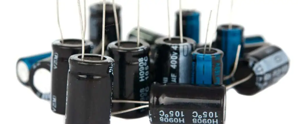
Decoupling and bypass capacitors are two of the most ubiquitous and important passive components used on printed circuit boards. They serve crucial functions in providing stable voltage regulation, filtering noise, and ensuring proper device operation.
While the terms “decoupling capacitor” and “bypass capacitor” are sometimes used interchangeably, there are in fact important distinctions between the two. Understanding the differences allows engineers to make informed design decisions when selecting and placing these capacitors.
This article provides an in-depth look at decoupling and bypass caps including:
- The functions and purposes of each type
- Key differences in behavior and characteristics
- Guidelines for selecting the proper capacitance and type
- Optimal placement considerations
- Modeling and simulating decoupling performance
- Mitigating decoupling issues like parallel and series resonance
- Real-world decoupling design examples
- Summary comparison of decoupling versus bypass caps
Read on to learn how proper utilization of decoupling and bypass capacitors can optimize circuit performance and prevent difficult-to-diagnose stability issues.
Functions of a Decoupling Capacitor

Decoupling capacitors, also known as bypass capacitors, serve several vital functions:
1. Maintain Steady Voltage to ICs
- During operation, ICs can draw current in abrupt spikes and surges
- This leads to fluctuations and noise on the DC power supply rails
- Decoupling caps maintain a stable voltage by supplying current to the IC during demand spikes
- They recharge quickly between spikes to remain ready for the next demand
2. Filter Noise
- Switching noise is generated on power rails due to digital logic transitions
- High frequency noise can impair circuit operation
- Decoupling caps filter noise through low impedance across a wide frequency spectrum
3. Reduce Ground Bounce
- Sudden current draw can cause ground potential to bounce or skew
- Capacitors between ground pins dampen bounce and skew
- This maintains signal integrity and noise margins
4. Control Impedances
- Decoupling caps help control impedances along power distribution network
- This avoids impedance discontinuities which reflect noise
- Proper impedance helps signals propagate without distortion
In essence, decoupling capacitors act like small localized energy reservoirs to supply current, filter noise, and maintain stable voltage to enable proper functioning of nearby ICs and devices. Next, we’ll see how bypass capacitors serve some similar but also differing functions.
Functions of a Bypass Capacitor
While bypass capacitors provide some similar functions as decoupling caps, key differences include:
1. Differential Noise Rejection
- Unlike decoupling caps directly from VDD to ground, bypass caps are placed in series from signal to ground
- This attenuates common-mode noise while allowing the signal to pass
- Useful for signals prone to picking up external interference
2. Band-Selective Filtering
- Proper bypass cap selection targets filtering of specific noise frequencies
- Values are chosen based on the frequency content to be rejected
- Provides more selective filtering compared to broadband decoupling caps
3. Cross-Talk Reduction
- In sensitive high-speed data links, capacitance between signal pairs reduces coupling
- Prevents signals from influencing one another
- Helps meet tighter timing margins at high data rates
4. Impedance Tuning
- Unlike decoupling caps from VDD to ground, bypass caps are in series with signals
- Can help fine tune characteristic impedance in transmission lines
- Allows better impedance matching through the signal chain
In summary, while decoupling caps focus primarily on power integrity, bypass capacitors address signal integrity objectives. With the functions covered, let’s compare some key characteristics.
Key Characteristic Differences Between Decoupling and Bypass Caps
While there is some overlap in functions, several key characteristic differences help distinguish decoupling and bypass capacitors:
| Characteristic | Decoupling Capacitor | Bypass Capacitor |
|---|---|---|
| Location | Close proximity between power and ground pins | In series between signal and ground |
| Purpose | Maintain steady voltage and filter power rail noise | Attenuate noise on signals and reduce cross-talk |
| Capacitance | High capacitance, small case sizes | Lower capacitance based on frequency response needs |
| Performance | Low ESR and impedance over wide frequency range | Targeted frequency response characteristics |
| Types | Ceramic, polymer, tantalum, niobium | Ceramic, film, mica, polystyrene |
| Packaging | Surface mount chips, leaded disks | Surface mount monolithic and stacked chips |
Some key points:
- Decoupling caps are placed close to IC power pins with short connections
- Bypass caps are placed along signal paths, often near terminals
- Decoupling caps need high capacitance in small sizes
- Bypass caps focus on targeted frequency performance
Now let’s look at selecting appropriate capacitance values for the different applications.
Selecting Capacitance Value
The target capacitance value depends greatly on whether the capacitor will serve a decoupling or bypass function:
Decoupling Capacitors
- Higher capacitance provides greater charge storage and noise filtering
- Target mounting inductance limits useable capacitance
- Typical sizes from 100nF to 10uF
- 0.1uF, 0.47uF and 1uF most common
Bypass Capacitors
- Chosen based on frequency response needed
- Lower values for higher frequencies, higher for lower frequencies
- 10nF to 100nF common for high speed serial links
- 0.001uF to 0.1uF typical for operational amplifier power pins
Here are some guidelines for selecting decoupling capacitance:
1. Determine Charge Requirements
- Estimate instantaneous charge needed during voltage spikes
- Factors: chip size, power draw, activity level
- More decoupling capacitance required for larger, more active ICs
2. Consider Distance to Power Supply
- Further distance to power source requires more local charge reservoir
- Increase decoupling caps for boards with single centralized regulator
3. Analyze Transient Loading
- Circuits with larger instantaneous current spikes need bigger decoupling caps
- Examine current draw waveform to determine worst-case transients
4. Factor in Inductance
- Total inductance to capacitor limits high frequency performance
- More capacitance can help compensate for higher inductance
With bypass capacitors, it is more important to select the proper capacitor technology for the desired frequency response. We’ll look more at passive component technologies later on.
Placement Considerations
Optimal placement is critical to maximize decoupling and bypass capacitor effectiveness.
Decoupling Capacitors
- Place immediately adjacent to power pins to minimize loop inductance
- Often locate multiple decoupling caps in parallel
- Position between IC and next decoupling cap in the distribution network
Bypass Capacitors
- Mount as close to the signal entry/exit point as possible
- Minimize distance between bypass cap and signal plane
- Place between signal source and noisy nodes
Some high performance PCB layout techniques include:
- Embedded decoupling caps within the inner layers
- Interdigitated capacitor arrays surrounding the IC
- 3D capacitor stacks combining multiple height values
- Periodic distribution of decoupling caps in grid patterns
Careful placement is key to realizing the full performance of both decoupling and bypass capacitors in the circuit.
Modeling and Simulating Decoupling

To analyze decoupling effectiveness, models are needed to simulate the PDN impedance behavior. Some approaches include:
IC Model
- Simple model: Current source, resistor, and inductor
- More complex: Resistor-capacitor (RC) network models IC and package
- Determines current load used to stress the PDN
PDN Model
- Capacitors, mounting inductance, plane impedance
- Vias, power and ground planes, interconnects
- Capture frequency-dependent impedance
Simulation Approaches
- SPICE circuit simulations
- Electromagnetic solvers for planes and components
- Specialized PDN impedance solvers
- IBM Power Delivery Network Analysis (PDNA) methodology
Simulations help predict resonances, identify insufficient decoupling, and determine impacts of board changes prior to a PCB layout. This enables proactive optimization of the decoupling network.
Mitigating PDN Impedances Issues
Decoupling capacitors help control PDN impedances, but potential issues must be addressed:
Parallel Resonance
- Caused by capacitors and voltage plane inductance
- Leads to unintended impedance peaks
- Mitigate by reducing loop inductance and/or increasing capacitance
Series Resonance
- Caused by capacitors and voltage plane capacitance
- Causes unwanted impedance nulls
- Mitigate by reducing plane capacitance and/or inductance
Spreading Inductance
- Currents spread non-uniformly in planes causing varying inductance
- Manage by proper decoupling placement, via distribution, and ground pours
Insufficient Decoupling
- Too little capacitance fails to supply transient current loads
- Add more decoupling caps near problem area
- Increase capacitance and reduce mounting inductance
Thorough PDN planning, simulation, and design reviews help identify and resolve decoupling issues before manufacturing the PCB.
Real-World Decoupling Capacitor Design Examples
Here are some examples highlighting decoupling design and optimization for different applications:
1. High-Speed Memory Interface
- DDR5 interface with memory controller IC
- High transient currents and noise at >5GHz speeds
- Target impedance below 0.5 ohm up to 5GHz
- Employed Pi-filter decoupling with two parallel 100nF MLCC caps and ferrite bead
- Used interdigitated capacitors adjacent to IC with ground vias in grid pattern
2. Automotive RADAR PCB
- 24 GHz MMIC (monolithic microwave IC) RF transceiver
- Extremely low supply noise required for phase coherence
- Leveraged embedded distributed capacitance below ICs
- Surrounded MMIC with multi-density stack of capacitors: 4x10nF, 2x100nF, 10uF tantalum
- Extensive power plane copper fills to reduce spreading inductance
3. High Power GPU
- High current transient loads up to 150A
- Target impedance below 5mohm up to 100MHz
- Employed land-side capacitors with bottom-side ground vias
- Grid of 4x1000uF POSCAP tantalum bulk capacitors
- 20x10uF ceramic capacitors distributed around processor
These examples showcase real-world applications of effective decoupling design techniques tailored to the specific requirements.
Comparison Summary: Decoupling vs. Bypass Capacitors
Here is a summary overview of the key differences between decoupling and bypass capacitors:
| Parameter | Decoupling Capacitor | Bypass Capacitor |
|---|---|---|
| Location | Near IC power pins | Along signal path |
| Purpose | Stable voltage, filter noise | Attenuate signal interference |
| Capacitance Value | Higher, depends on IC current demand | Lower, based on frequency response |
| Performance | Low impedance over wide frequency band | Targeted filtering for noise frequencies |
| Types | Ceramic, polymer, electrolytic | Ceramic, film, mica |
| Packaging | Surface mount, through-hole | Monolithic and stacked surface mount |
| Resonances | Mitigate parallel and series resonance | Less susceptible |
| Modeling | PDN impedance, IC transient loads | Source and load termination |
This summarizes some of the key differences in a concise comparison table. Both capacitor types are critical PCB components but address distinct requirements.
Frequently Asked Questions
Here are some common FAQs regarding decoupling and bypass capacitors:
Q: Can a bypass capacitor be used for decoupling and vice versa?
In some cases yes, but performance may be compromised compared to using the optimal type. The distinguishing factors are location relative to power vs. signal pins and wide-band vs. selective frequency response characteristics.
Q: How are bypass/decoupling capacitors modeled in circuit simulation?
Decoupling caps are modeled as part of the full PDN with emphasis on equivalent series inductance. Bypass caps can be modeled as simple capacitive sources with appropriate frequency-dependent impedance characteristics.
Q: What testing is done to characterize decoupling capacitor performance?
Parameters like equivalent series resistance/inductance and impedance versus frequency may be tested to characterize decoupling effectiveness across operating frequency ranges.
Q: How can I calculate the target impedance for my PDN?
Factors like anticipated load transient current, switching noise tolerance, and voltage margin are used to estimate the maximum allowable PDN impedance based on voltage deviation limits.
Q: What construction techniques help reduce inductance?
Shorter traces, interdigitated capacitors, embedded capacitance, and vias in tight grid patterns all help minimize mounting loop inductance.
Conclusion
Decoupling and bypass capacitors address unique but equally vital functions in maintaining proper circuit operation. As PCBs continue advancing to faster speeds and lower voltages, utilizing the appropriate capacitor technologies and design techniques is imperative. Understanding the key distinctions between decoupling and bypass caps will enable engineers to make informed design decisions.
The detailed comparisons and examples in this article equip PCB designers with deep knowledge to deploy decoupling and bypass capacitors effectively. By leveraging the right capacitor solutions tailored to each application’s specific needs, robust performance and stability can be achieved.