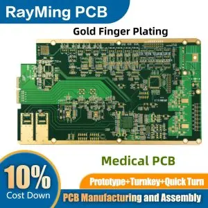
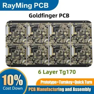
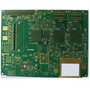
In modern electronics, seamless communication between circuit boards is essential for optimal device performance. Gold finger PCB technology serves as the backbone of this interconnection, enabling reliable data transfer and power distribution across countless electronic devices. From smartphones to industrial machinery, gold finger PCBs ensure consistent connectivity that users depend on daily.
What is a Gold Finger PCB?
A gold finger PCB refers to a printed circuit board featuring gold-plated edge connectors along one or more edges. These specialized connectors, also known as edge fingers or edge connectors, create reliable electrical connections when inserted into corresponding slots on motherboards or other PCBs.
The term “gold finger” derives from the appearance of these connectors – they resemble golden fingers extending from the PCB edge. Gold is used for the connecting points along a PCB because of the alloy’s superior conductivity and exceptional resistance to corrosion and wear.
Key Components of Gold Finger PCB Design
Base Material: The PCB substrate, typically FR4, provides structural support and insulation between conductive layers.
Copper Traces: Conductive pathways that connect internal circuits to the edge connector pads.
Nickel Underlayer: Applied before gold plating to enhance adhesion and provide additional corrosion protection.
Gold Plating: The final surface finish that ensures optimal conductivity and durability.
Types of Gold Plating for PCB Edge Connectors
Understanding the different gold plating options is crucial for selecting the right gold finger PCB for your application.
Electroless Nickel Immersion Gold (ENIG)
ENIG is more cost-effective and easier to solder than electroplated gold, but its soft, thin (typically 2-5u”) composition renders ENIG unsuitable for the abrasive effects of circuit board insertion and removal. ENIG works well for applications with minimal connector cycling.
Advantages:
- Lower cost compared to hard gold
- Excellent solderability
- Uniform thickness across complex geometries
Limitations:
- Not suitable for frequent insertion/removal
- Thinner plating offers less wear resistance
Electroplated Hard Gold
Electroplated hard gold is solid (hard) and thick (typically 30u”), thus more ideal for the abrasive effects of constant PCB usage. This makes it the preferred choice for applications requiring frequent connector cycling.
Advantages:
- Superior wear resistance
- Supports up to 1,000 insertion cycles
- Enhanced durability for high-usage applications
Applications:
- Computer expansion cards
- Memory modules
- Industrial control systems
Gold Finger PCB Manufacturing Process

The manufacturing of gold finger PCBs requires precise control and adherence to industry standards to ensure optimal performance and reliability.
Step-by-Step Manufacturing Process
1. PCB Fabrication The base PCB is manufactured according to design specifications, with careful attention to trace routing and pad placement for the edge connectors.
2. Solder Mask Application The edge finger plating process is performed after the application of the solder mask and before the surface finish. The solder mask must be properly positioned to avoid interference with the gold finger areas.
3. Nickel Plating First, 0.004 to 0.008 mil of nickel is plated onto the connector edges of the fingers. This underlayer provides excellent adhesion for the gold plating while offering additional corrosion protection.
4. Gold Plating Later, 0.04 to 0.08 mil of hard gold is plated over the nickel. The gold is usually mixed with cobalt for increasing the surface resistance.
5. Edge Beveling The connector edges are beveled at specific angles to facilitate smooth insertion into mating connectors. Available beveling angles include 20°, 30°, 45°, and 60°.
Quality Control and Testing
Visual Inspection: Each gold finger PCB undergoes magnified visual inspection to ensure smooth, clean surfaces free from defects.
Tape Test: Adhesion testing using specialized tape to verify proper gold plating adhesion to the substrate.
Thickness Measurement: Precise measurement of gold plating thickness to ensure compliance with specifications.
Read more about:
Design Specifications and Standards for Gold Finger PCBs
Proper design is crucial for manufacturing reliable gold finger PCBs that meet performance requirements and industry standards.
Critical Design Rules
Spacing Requirements: Plated through-holes should not be situated close to them and should maintain adequate clearance to prevent manufacturing issues.
Trace Width: Should be connected with 8 mil conductor traces. It makes manufacturing easier while ensuring proper current carrying capacity.
Solder Mask Clearance: Should be kept at a distance from solder mask or silkscreen printing to prevent contamination during the plating process.
Industry Standards and Specifications
Chemical Composition: The gold plating should consist of 5-10% cobalt for maximum rigidity across the board edges.
Thickness Standards: The plating thickness of gold/edge fingers must fall between 0.002-0.005 mil for optimal performance and durability.
Dimensional Tolerances: Can be easily placed on one or both sides of a board to a depth of 1 inch from the outer edge.
Applications of Gold Finger PCBs Across Industries

Gold finger PCBs enable connectivity solutions across diverse industries and applications, each with specific requirements for performance and reliability.
Computer and Consumer Electronics
Memory Modules: RAM and storage devices utilize gold finger PCBs for high-speed data transfer between memory and the motherboard.
Expansion Cards: Graphics cards, sound cards, and network adapters rely on gold finger connections for power and data transmission.
Mobile Devices: Smartphones and tablets use miniaturized gold finger PCBs for internal component interconnection.
Industrial and Automotive Applications
Control Systems: Industrial control system: Connection to different devices (factory robot arm, high-end consumer electronics, computerized industrial machines, etc.)
Automotive Electronics: Engine control units, infotainment systems, and safety modules utilize gold finger PCBs for reliable operation in harsh environments.
Telecommunications Infrastructure
Network Equipment: Telecommunication industry: Connection for network data transfer (communication adapter) requires robust gold finger PCBs for continuous operation.
Base Stations: Cellular infrastructure equipment depends on gold finger PCBs for signal processing and transmission.
Advantages of Gold Finger PCB Technology
Understanding the benefits of gold finger PCBs helps in making informed decisions for electronic design projects.
Superior Electrical Performance
High Conductivity: Gold’s excellent electrical conductivity ensures minimal signal loss and optimal performance.
Low Contact Resistance: Gold plating maintains consistent electrical contact even after multiple insertion cycles.
Mechanical Durability
Wear Resistance: Hard gold plating withstands repeated insertion and removal cycles without degradation.
Corrosion Protection: Gold’s chemical inertness prevents oxidation and maintains long-term reliability.
Cost-Effective Connectivity
Simplified Assembly: Edge connector design eliminates the need for additional connectors and cables.
Space Efficiency: Compact form factor saves valuable PCB real estate in miniaturized devices.
Choosing the Right Gold Finger PCB Solution with RAYPCB

When selecting a gold finger PCB manufacturer, several factors contribute to project success and long-term reliability.
Design Consultation Services
RAYPCB offers comprehensive design review services to optimize gold finger PCB layouts for manufacturability and performance. Our experienced engineers evaluate trace routing, connector placement, and mechanical constraints to ensure optimal results.
Manufacturing Capabilities
Precision Plating: State-of-the-art electroplating equipment ensures consistent gold thickness and quality across all production volumes.
Quality Assurance: Rigorous testing protocols verify electrical performance, mechanical durability, and adherence to industry standards.
Flexible Production: From prototype quantities to high-volume production runs, RAYPCB accommodates diverse project requirements.
Technical Support
Application Engineering: Expert guidance on gold finger PCB selection, design optimization, and application-specific requirements.
Documentation: Comprehensive technical documentation including specifications, test reports, and compliance certifications.
Future Trends in Gold Finger PCB Technology
The evolution of gold finger PCB technology continues to drive innovations in electronic connectivity and performance.
Miniaturization Advances
As devices become smaller and more complex, gold finger PCBs are evolving to support higher density connections with reduced footprints. Advanced manufacturing techniques enable finer pitch connectors and thinner profiles.
Enhanced Materials
Research into alternative plating materials and substrate technologies promises improved performance characteristics while potentially reducing costs.
Environmental Considerations
Growing emphasis on sustainability drives development of environmentally friendly plating processes and recyclable materials for gold finger PCBs.
Frequently Asked Questions (FAQ)
What is the difference between ENIG and hard gold plating for PCB edge connectors?
ENIG (Electroless Nickel Immersion Gold) is thinner and more cost-effective but suitable only for low-cycle applications. Hard gold plating is thicker, more durable, and designed for applications requiring frequent insertion and removal cycles.
How many times can a gold finger PCB be inserted and removed?
With proper hard gold plating, a gold finger PCB can typically withstand up to 1,000 insertion and removal cycles while maintaining reliable electrical connectivity.
What are the standard thickness requirements for gold finger plating?
The gold plating thickness for PCB edge connectors typically ranges from 0.002 to 0.005 mil (0.05 to 0.127 micrometers), with specific requirements depending on the application and expected duty cycle.
Can gold finger PCBs be manufactured on both sides of the board?
Yes, gold finger PCBs can feature edge connectors on one or both sides of the board, depending on the design requirements and application needs.
What is the purpose of beveling on gold finger PCBs?
Beveling creates angled edges on the connector fingers to facilitate smooth insertion into mating sockets. Common bevel angles include 20°, 30°, 45°, and 60°.
How do I ensure proper spacing between gold fingers and other PCB features?
Maintain at least 1.0mm clearance between gold fingers and plated holes, SMD components, or pads. Keep solder mask and silkscreen printing away from the gold finger areas to prevent contamination.
What industries commonly use gold finger PCBs?
Gold finger PCBs are widely used in computer hardware (memory modules, expansion cards), telecommunications equipment, industrial control systems, automotive electronics, and consumer devices.
How does RAYPCB ensure quality in gold finger PCB manufacturing?
RAYPCB implements comprehensive quality control including visual inspection, adhesion testing, thickness measurement, and electrical testing to ensure each gold finger PCB meets specifications and industry standards.


