Introduction
A power supply is a crucial component that converts power from a source to the regulated voltages required by electronic circuits and systems. The proliferation of electronic devices has led to power supplies being ubiquitous, ranging from chargers for mobile phones to high capacity supplies in data centers. Designing a proper power supply requires expertise in multiple engineering domains encompassing power electronics, analog design, control theory, and thermal management.
This article provides a step-by-step guide on designing a power supply covering aspects like topology selection, power stage design, feedback and control, safety standards compliance, thermal design, and electromagnetic compatibility. By following the structured design methodology, electrical engineers can develop reliable and efficient power supplies tailored to their application needs.
Functional Requirements
Defining the right specifications and functional requirements is the critical first step that sets the overall direction for the power supply design.
Input Voltage Range
The expected input voltage range should be specified, including minimum, nominal, and maximum voltages. Common input ranges are 5V, 12V, 24V, or 48VDC derived from rectified mains AC or batteries. Wider input ranges require designs that can maintain regulation over the span.
Output Voltages and Currents
The desired output voltages and load currents should be specified. For multiple outputs, cross-load dependencies and sequencing needs must also be considered. Safe margins above nominal loads should be included for fault conditions. Prioritizing critical outputs helps allocate design resources effectively.
Efficiency Targets
Required full load and partial load efficiencies at nominal voltages determine components selection and loss budgeting. Light load efficiency is also critical for new energy-efficiency standards.
Power Density Targets
The desired power density (watts/cubic inches) influences how compactly the design must be packaged. It requires trade-offs with efficiency and thermal performance.
Safety and Emissions Compliance
Regulatory standards like medical and IT equipment safety, conducted emissions, and radiated emissions compliance must be considered.
Reliability Requirements
Requirements like MTBF, expected service life, and environmental survival ranges help guide design choices for component deratings and redundancies.
Control Characteristics
Needs like remote control, sequencing, telemetry, and margining control influence digital control and communication features.
Topology Selection
The choice of power conversion topology sets the foundation for meeting the design goals. Different topologies have inherent advantages and limitations.
Linear Regulator
A linear regulator maintains output voltage by dropping excess input voltage across a series pass element. The advantages are simplicity, low noise, and fast response. But poor efficiency at lower output voltages makes them unsuitable for high power applications.
Switching Regulator
Switching converters use semiconductor switches to transfer chunks of energy to the output in a controlled pulsed manner. Switching loss is lower than a linear regulator, allowing high efficiency conversion even for large voltage drops. However, switching noise requires careful filtering.
Various sub-classes of switching regulators offer further topological choices:
- Buck Converters: Used for step-down conversion from higher input to lower output voltage.
- Boost Converters: Used for step-up conversion from lower input to higher output voltage.
- Buck-Boost Converters: Allows both step-down and step-up conversion flexibly.
- Isolated Topologies: Flyback, forward, push-pull, and full-bridge converters use transformers for isolation and multiple outputs.
Selection criteria include required conversion ratio, complexity, component stresses, efficiency, and isolation needs.
Resonant and Soft-Switching Topologies
Resonant converters and quasi-resonant soft-switching schemes reduce switching losses allowing very high efficiency conversion. However, the added complexity may not justify gains for lower power applications.
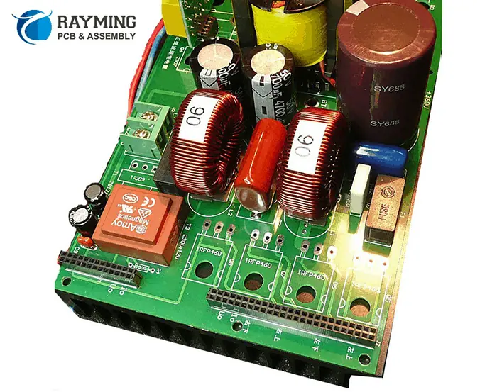
Power Stage Design

The power stage handles the actual power conversion between input and output. It consists of elements like switches, diodes, inductors, transformers, and capacitors.
Semiconductor Switch Selection
MOSFETs and IGBTs are suitable semiconductor switch choices for power supplies below 500W. High current capability MOSFETs allow simpler synchronous rectifier buck designs. Above 500W, IGBTs tend to be more robust. Availability of integrated power modules with paralleled devices simplifies high current designs.
Passive Components
- Inductors: Value selection involves tradeoffs between ripple, response time, and component size. Core materials and shapes like toroids or pot cores optimize efficiency.
- Transformers: Core geometry, materials, gap design, winding techniques, and layered or interleaved windings affect performance.
- Capacitors: A mix of electrolytic and multilayer ceramic capacitors provides bulk capacitance and high frequency bypassing.
Snubbers and Clamps
Snubbers like RC networks suppress voltage spikes across switches during switching transitions. Clamps help limit overvoltage events.
Layout and Parasitics
Careful component placement and routing minimizes the length of high current paths to reduce parasitic inductance and resistance. Separating noisy switching nodes from sensitive analog areas is necessary.
Feedback and Control
To maintain stable regulated output voltages, feedback control forms a closed loop system adjusting PWM switching patterns based on output voltage deviations from the reference.
Voltage Dividers
Properly designed resistive divider networks scale output voltages to levels acceptable for the feedback IC. Filtering may be required for noise reduction.
Feedback IC
Specialist ICs provide operational amplifier, pulse width modulation (PWM), compensation circuits and protection features needed for robust control and regulation of switching converters.
Compensation Network
This provides the corrective feedback and stability for the control loop. The network sets gain crossover and phase margin by shaping the IC loop gain to target stable response with adequate noise immunity.
Digital Control
Incorporates monitoring, diagnostics, communication, and adaptive tuning functions via a microcontroller. This allows sophisticated control algorithms and remote user interfaces.
Protection Features
Protection safeguards the power supply and connected load during abnormal conditions. Common protections include:
- Overvoltage protection – Shuts down supply if output exceeds preset safe threshold.
- Undervoltage protection – Shuts down supply if output sags excessively under minimum level.
- Overcurrent protection – Shuts down supply if load current exceeds set limit indicating a short circuit.
- Over temperature protection – Shuts down supply if internal temperatures rise beyond safe operating limit.
- Input under/over voltage lockout – Disables output if input is outside operating range.
- Redundancy – Secondary backup units takeover upon failure detection
- Surge and transient protection – MOVs, RC snubbers absorb incoming surges on input.
Thermal Design
Generating substantial heat is an inherent consequence of power conversion. Effective thermal management is vital for reliable operation and safety.
Power Dissipation Analysis
The distribution of losses in switches, magnetics, and other components determines cooling requirements. Analytically derived and validated through simulations.
Heatsink Design
Heatsinks provide convective cooling matched to the power dissipation profile. Fin geometry, airflow passage design, heat pipe augmentation, and interface materials influence heatsink performance.
Airflow and Ventilation
Fans and airflow ducting maintain sufficient directed airflow through heatsinks and the housing. Intake and exhaust vents are designed to utilize natural convection also.
Thermal Interface Materials (TIMs)
TIMs like thermal pads, greases, or phase-change compounds improve heat conduction from components to heatsinks.
EMI/EMC Design

Switching power supplies generate significant high-frequency noise requiring careful mitigation to meet EMI limits and prevent conducted/radiated interference with other devices.
Input Filtering
Pi-filters and ferrite beads supress current-driven differential mode noise propagating from the AC input to the power stage.
Output Filtering
Capacitors, ferrites, and LC filters clean up switched-mode noise in DC output to avoid contaminating sensitive downstream circuits. Shielding on cables also reduces emissions.
Circuit Partitioning
Keeping noisy power circuits physically separate from analog and digital control areas through partitioning, shielding and isolation helps reduce interference coupling.
EMI Reduction Techniques
Spread spectrum frequency modulation, soft-switching, snubbers, and proper grounding and shielding all help minimize emissions at source.
Shielding
Proper enclosure shielding and correct filter feedthrough component installation is critical to contain radiated emissions. PCB stitching vias help shield leakage from gaps in ground planes.
Physical Design and Packaging
The physical design and packaging determines the integrity and usability of the power supply.
Enclosure and Chassis
The enclosure provides mechanical support, safety isolation between circuits and users, shielding for EMI control, and channels airflow for ventilation.
PCB Layout
PCB component placement and routing optimizes current flows, minimizes parasitics, provides noise isolation between stages, and facilitates servicing and manufacturability.
Cables, Connectors, Indicators
Cabling connects internal electronics to external interfaces like the AC inlet, DC output terminals, and control connectors reliably. Indicator lamps display enabled/fault statuses.
Environmental Protection
Conformal coatings protect against dust, moisture, and temperature extremes. Potted enclosures improve vibration and shock survivability.
Compliance Testing and Certifications
Verification testing ensures the design meets requirements and passes mandatory certifications for the target application and market.
Functional Testing
Confirm basic functionality across operating conditions of loads, voltages, temperatures, and frequencies. Burn-in reliability testing stresses components.
Safety Standards
Certifications like UL, CSA, ENEC for end-use product safety requirements including insulation, fault tolerance, construction, marking.
EMI and EMC
Testing for conducted and radiated emissions, immunity to interference, and surge withstand verifies compliance to FCC, CE standards.
Environmental Tests
Verifies operation under challenging environmental stresses like temperature, humidity, vibration, shock, salt-fog, and ingress protection.
Conclusion
Designing reliable, efficient, and fully-featured power supplies requires expertise across multiple engineering domains coupled with practical experience guiding design choices. A structured approach allows methodically addressing requirements and making sound trade-offs from topology selection to packaging. Utilizing rigorous compliance testing ensures regulatory and safety standards are satisfied before product release. The demand for well-designed cost-effective power supplies will only grow given their ubiquitous role in powering modern technological advances.
Frequently Asked Questions (FQA)
Q1: What is the difference between linear and switch mode power supplies?
A1: Linear power supplies regulate output voltage by dropping excess input voltage across a pass element, allowing continuous output current but with poor efficiency at lower output levels. Switch mode supplies chop input voltage into pulses using semiconductor switches, converting it more efficiently through an inductor into lower average output voltage.
Q2: How do you ensure stable voltage control in switch mode power supplies?
A2: A negative feedback control loop compares actual output voltage against a precision reference using an error amplifier. The loop compensates by increasing or decreasing the duty cycle of the PWM switched input to maintain the required output voltage irrespective of changing load conditions.
Q3: What protections should be incorporated in a well-designed power supply?
A3: Protections for over-voltage, under-voltage, over-current, over-temperature, input voltage out-of-range conditions should be implemented. These detect fault conditions and safely shut down or restart the power supply as appropriate. Redundant operation can also provide backup protection.
Q4: What construction techniques help reduce EMI from power supplies?
A4: Shielding the power supply enclosure, minimizing gaps in return paths, keeping noisy circuits physically separate from sensitive ones, using appropriate input and output filters, PCB partitioning, as well as spread spectrum and soft-switching techniques reduce emitted and conducted EMI.
Q5: What are some important regulatory approvals and certifications for power supplies?
A5: Safety certifications like UL, CSA, ENEC, CE are mandatory for commercial power supplies. FCC, CISPR compliance is required for radiated and conducted emissions. Specialized medical and industrial equipment certifications may also be required depending on the application.