Rogers Material PCB – Rogers 4003C and Rogers 3003

rogers board

Eestimate Rogers 4003c and Rogers 3003 PCB Price,Send email to Sales@raypcb.com 

RayMing is a rogers 4003c pcb and rogers 3003 PCB manufacturer that can offer high-frequency circuit board manufacturing services with competitive prices. Simply buy a good High-Frequency PCB at a reasonable price from us and get the datasheet from our suppliers who can work for you.

rogers 4003

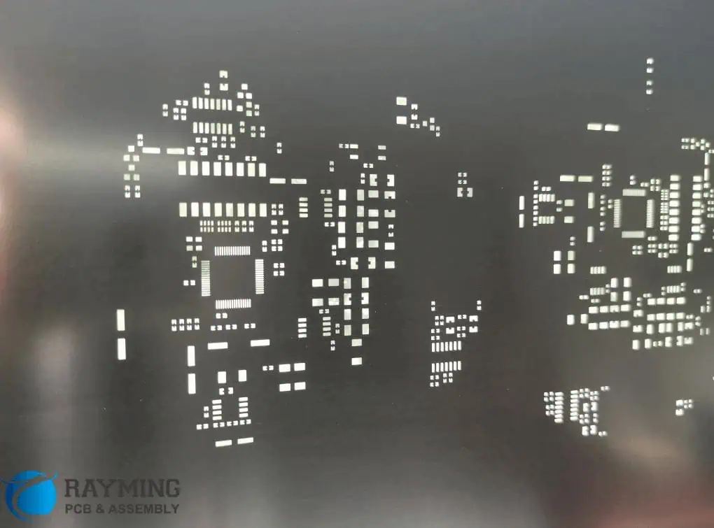
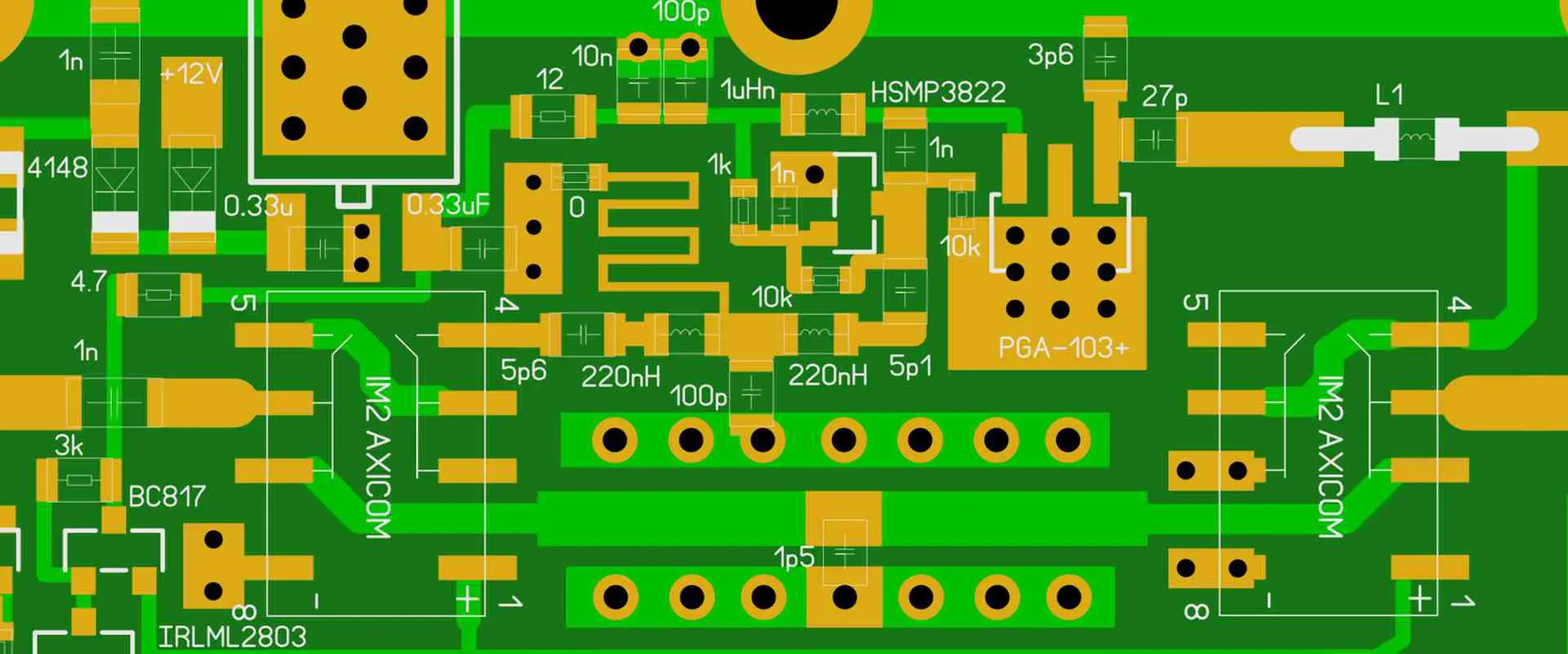
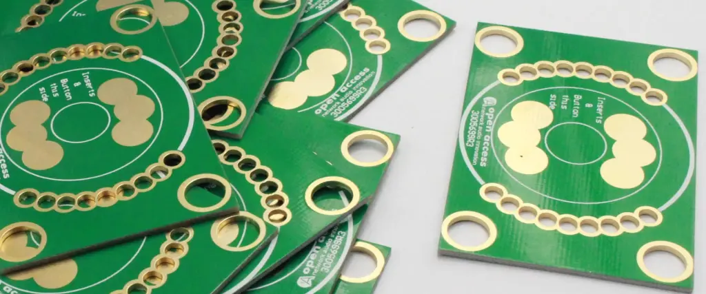
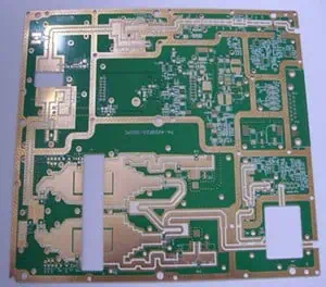
Rogers RO4003 PCB /Rogers 4003C

The Rogers RO4003 material can be removed with conventional nylon brushes. Prior to copper plating without electricity, no special treatment is required. The plate must be treated with conventional epoxy/glass processes. Usually, the removal of drilled holes is not necessary because the high TG resin system (280 ยฐ C + [536 ยฐ F]) is not prone to discoloration during drilling. The resin can be removed using a standard CF4 / O2 plasma cycle or a double pass through an alkaline permanganate process if the stain results from aggressive drilling practices.

YouTube video

The surfaces of the plates can be mechanically and/or chemically prepared for photoprotection. Standard aqueous or semi-aqueous photoresists are recommended. Any of the commercially available copper wipers can be used. All filterable or photographic solder masks normally used in epoxy/glass laminates adhere very well to the surface of Rogers RO4003. Mechanical washing of the exposed dielectric surface prior to application of the solder mask and a designated โ€œregisteredโ€ surface should avoid optimal bonding.

HASL and REFLOW:

The baking requirements of RO4000 materials are comparable to those of epoxy/glass. In general, equipment that does not bake epoxy/glass plates does not need to bake RO4003 plates. For installations that make epoxy/bake glass as part of the normal process, we recommend cooking at 300 ยฐ F 250 ยฐ F (121 ยฐ C-149 ยฐ C) for 1 to 2 hours. RO4003 contains no flame retardant. It is understood that plates enclosed in an infrared (IR) unit or operating at very low transport speeds can reach temperatures in excess of 700 ยฐ F (371 ยฐ C). RO4003 can start burning at these high temperatures. Systems that still use IR reflow units or other devices that can reach these high temperatures should take the necessary precautions to ensure that there are no risks.

Life of life:

High-frequency laminates can be stored indefinitely at room temperature (55-85 ยฐ F, 13-30 ยฐ C) and humidity. At room temperature, the dielectric materials are inert at high humidity. However, metal coatings such as copper can be oxidized when exposed to high humidity. Standard pre-cleaning of PWB can easily remove corrosion from properly stored materials.

ROUTE:

RO4003 material can be machined using tools and hard metal conditions commonly used for epoxy/glass. The copper foil must be removed from the guide channels to prevent smearing.

Rogers Ro3003 / Rogers 3003

rogers 3003

Ro3003 is one of Rogers PCB materials are ceramic filled PTFE composites for use in the commercial microwave and RF applications. This family of products is designed to provide exceptional electrical and mechanical stability at competitive prices. Rogers Ro3003 is an excellent dielectric constant stability over temperature, including the elimination of the dielectric constant change that occurs at room temperature with PTFE glass materials. In addition, Ro3003 laminates have a low loss factor of 0.0013 to 10 GHz.

Features and Benefits

  • Car radar
  • RF Coupler
  • Cost-sensitive aerospace applications
  • GPS antennas
  • Low Dielectric Losses: Laminates can be used in applications up to 77 GHz
  • Excellent mechanical properties against temperature: reliable multi-layer plate constructions and tape lines
  • Uniform mechanical properties for a wide range of dielectric constants: ideal for multi-layer plate designs with a range of dielectric constants and suitable for use with hybrid designs of multilayer epoxy glass plates.
  • Stable temperature and frequency stable dielectric constant โ€“ ideal for bandpass filters, microstrip antennas, and voltage controlled oscillators
  • Low in-plane Coefficient of Coefficient Coincidence: provides more reliable surface mountings, ideal for temperature-sensitive applications and excellent dimensional stability
  • The manufacturing process in volume: economic price rolled
  • Compatible lead-free process

Rogers RO3003 is a ceramic-filled PTFE composite/laminate used in commercial microwave and RF applications. It offers excellent stability with a dielectric constant of 3 to 40 GHz at room temperature. The material has a dissipation factor (Df) of 0.0013 to 10 GHz and is ideal for bandpass filters, microstrip antennas, and voltage controlled oscillators. High-performance material for RF and microwave circuitsRogers RO3003 High-frequency laminate for the generation of microwave prototypes and high-frequency circuits. These materials have a very low dielectric loss to use up to 40GHz. We sell two sizes of 4.5 x 6 inches and 9 x 6 inches to keep the enthusiastโ€™s cost.

Rogers RO3003

  • Dielectric constant: 3.00
  • Loss factor: 0.0013
  • Substrate thickness: 0.02 โ€œ(0.5 mm)
  • The thickness of copper: 0.5 ounces
  • Small size = 4.5 โ€œx 6โ€
  • RO3000 printed circuits

Typical Applications

  • Automotive radar applications
  • Global Position Satellite Antennas
  • Mobile telecommunication systems: power amplifiers and antennas
  • Patch antenna for wireless communication
  • Satellites for direct transmission
  • Data link in cable systems
  • Remote meter readers

More Reading Guilde:

Regarding the manufacturing of Printed Circuit Boards, there are different materials to use. Among the most common materials used in producing PCBs are the Rogers 4003 and Rogers 3003. There is a question people frequently ask. Are there differences between Rogers 4003 and Rogers 3003? You should never assume that you can make both materials from the same components. Use a standard and high-frequency material for all PCBs. It is very crucial for us to thoroughly give more explanations on the distinctive characteristics of the Rogers 4003 PCB material. Many often assume its properties are the same as the Rogers 3003.

Here, youโ€™ll get an explanation on the variance between the two components of the Rogers materials. Readers will learn more about the Rogers 4003 and as well as the 3003. Both have properties that you cannot find in some other PCB materials. This is because of their distinctions. You have the right piece in your hands. Simply learn more about PCB designs.

What Are Rogers Materials?

rogers-laminates
Rogers Material

In this part of the article, we will begin with what the Rogers PCB materials are. The Rogers PCBs are majorly high frequency and hydrocarbon ceramic materials. It aids an upgraded development in production and its result is profound. It also decreases cost printed construction that enables its heating steady. Therefore, it diminishes the electrical damage or cost that is some wave loss.

The Rogers PCB has some components made from the Flame Retardant Level 4. This FR4 is present in several PCBs. They are some components of reflector fiber or adhesive which come with amber foil layered on either a particular area or both surfaces.

These PCBs play an essential role in the manufacturing of electronic devices. That is why it is crucial to selectively pick the right components in the production of PCB. Every designer or engineer must become familiar with the right material for PCB. This is because they mostly play a role in the works of designs and construction of electronic products.

These boards possess some high-frequency properties. The Rogers materials are more highly-priced than fiber meth. Also, these materials are about 6.15 DK or 11 DK. The Rogers PCB is always durable. Also, it often comes with a steady temperature. It is not the kind of PCB that has a very unreliable component.

The Rogers PCB elements have about three main groups. These three categories include the laminates, bonding substances, and the metal facing or lining. The metal lining is a type of protective covering for the PCB. It has some resistive settings. The bonding substances include electrically heating glue and prepreg.

You cannot ignore the world of automation as well as aeronautical engineering. In the military, this is important for jamming systems. For amplifiers, and anything related to RF engineering, this is also useful.

Read about Rogers SYRON 7000 PCB here

What is Rogers 4003?

The Rogers 4003 Printed Circuit Board is a PCB model that operates on a woven reflecting surface. You support it with either tile or hydrocarbon. Rogers 4003 is a laminate that offers high-speed performance. This is as a result of its low dielectric loss and tolerance. This high-frequency PCB has some great features. These include

  • A low thermal coefficient of dielectric constant
  • Great dimensional stability
  • Other mechanical and electrical properties

This PCB features some stunted thermal measurement of dielectric regularity. It also offers little in-plane extension quantity, and superb depth stability.

The importance of the RO4003 is well known. It is also crucial for designers to know the worth of this PCB to designs. It is useful in FR4 production. This includes multifaceted PCB development. It also has some sturdy lead loose braze modifying compatibility. From the creation along with material expansion, circuit making to the last constituent assembly, engineers see to the fabrication of this PCB.

RO4003 PCB has a small dielectric constant because of the little mislaying of the setting up material. The element is RO4003 C. This element comes with some compact check on top of the DK. This element misplaces extremely tiny heat intensity. However, it is the most essential for production.

Benefits of Rogers 4003

You can use the Rogers 4003 on RF microwaves due to its thermal and electrical properties. This PCB features some very important benefits. These include:

Unfluctuating electrical criteria

This is one of the key features of this particular PCB. Its electrical components are firm. This makes it very solid and durable. This is why designers and engineers can maximally use this PCB for electronic equipment.

Its dielectric resistance and dropping are quite flat

In a way, it becomes fitting for applications that require colossal frequency conduct. This PCB can work perfectly for colossal tech devices that automatically use high frequency.

One can detach the RO4003 PCB component using some regular fiber brushes

Ordinarily, you donโ€™t need any exceptional procedure to precede the copper lamination or covering in the absence of electricity. This PCB serves multiple functions. Generally, you can use it for Microstrip. Also, it is great for cellular radix terminal antennas along with power ampere.

Ideal for high-frequency applications

Due to the great properties of Rogers 4003, you can use them for high-frequency applications. This is one good reason why RF microwave circuit engineers prefer it. It also plays a vital role in the military, automobile, and telecommunication industries.

Other Facts about RO4003

There are several other facts about the Rogers 4003, users must know. First, is that an expert electronic designer has to supervise the fabrication process of this PCB. Its features are simple and its design development is straightforward. It possesses some unconventional electromagnetic prevalence. Interestingly, the Rogers 4003 is also useful for applications requiring frequencies more than 300MHz.

High-frequency PCBs were originally helpful in military operations. With development, they gradually become more accessible in medical operations. It is also accessible in contemporary industrial operations. This is seen in all advanced communication applications across the globe.

This PCB is not only appropriately useful for HF applications. It could be present in any application as long as it can work effectively. The RO4003 PCB possesses some excessive aversion to heat. It also comes with low power or current sound. Besides, it has little water receptiveness, close effusiveness related to copper cart as well as low dissolution agent.

Other notable features of this PCB include its possession of high fiber conversion febricity or condition. It also comes with exceptional magnitude steadiness. Above all, it is not so difficult to produce in huge amounts. This makes it so popular in its usage among engineers.

It is paramount to know about the Rogers 4003 dielectric constant of this PCB. The dielectric material of any PCB is some element that encloses the coating of a PCB. This could possess some low electric gravity or voltage. These components are different. They may be some specific alloy oxides, fiber, phlogopite, porcelain, or some ductile.

Limitations of Rogers 4003

The Rogers 4003 has some restrictions. This is owing to the elements used in its fabrication process. The components are fixed on hydrocarbons. The effect primarily is that the hydrocarbon element is prone to certain changes.

This is in relation to its risk to oxidative conditions for an extended period of time. You must not overly expose the RO 4003 to harsh thermal expansion. Its dielectric features start to alter gradually in such a scenario.

The solder mask on Rogers 4003 PCB basically halts terse circuits in the PCB. Although the use of a solder mask is not a must for Roger 4003 PCB. Irrespective of the distribution of shielding to the PCB, the solder mask can also discordantly change the conduct of the PCB. That is the reason one may consider using the liquid form of a solder mask.

What is Rogers 3003?

The Rogers 3003 is also a high-frequency PCB. Its elements are PTFE compounds meant for use in some materialistic microwave with an RF operation. The Rogers 3003 is common in designs. This is because it is durable and quite affordable.

It gives excellent solidity with some dielectric constant which is about 3 to 40 GHz within room febricity. The element has a dissolution component of not less than 0.0013 to 10 GHz. Also, it is perfect for band pass filters, microstrip antennas, as well as electron-regulated oscillators.

Rogers 3003 is a high-frequency, ceramic-filled PTFE laminate applicable for use in RF and microwave applications. This laminate belongs to the RO3000 series. This is why it possesses consistent mechanical properties irrespective of the dielectric constant needed.

The RO3003 possesses some unique features of a dielectric constant of 3.00. Others include a loss agent of about 0.0013 with its substrate diameter of about 0.02. The density of its copper is within the range of 0.5 ounces.

Its enlargement measurement is equivalent to the extension measurement of copper. This additionally makes the components possess some great proportional firmness. It is noteworthy that its regular plate reduction is not more than 0.5 inches. Its Z center line CTE is about 24 ppm. This is greatly unique to this PCB. Thus, it supplies very good coating via hole dependability irrespective of being in a severe thermal domain.

Benefits and Features of Rogers 3003

Interestingly, there are so many things to know about this PCB. Let us consider where you can use this extensively. You can use it for locomotive sonar systems. Also, you can use it for mobile telecommunication operations which involve power amplifiers as well as antennas. You can also use it for satellites meant for straight transferral. It has a data connection in cord techniques.

This PCB has some superb automatic features against cold. It has trusted manifold plate creation with tape cords or bars. It comes with several advantages for designs. These benefits make it easier for engineers and designers to construct without challenges. It possesses some cost-responsive aerospace systems.

It has invariable and steady mechanical components for an extensive array of dielectric constants. Also, it is most applicable for use with crossed and blended patterns of a multifaceted bond of fiber plates.

This PCB is one of the best for electrical circuits. It allows for the free flow of electrons. It can also regulate the temperature in a certain environment. Among the Rogers PCBs, this is arguably one of the most common types.

One of the major reasons engineers prefer it is its low dielectric loss. This board is good at high temperatures. It can work within a range of not less than 10GHz. This design is also for good mechanical support. It has some polytetrafluoroethylene elements present in it.

Modern industrial science and systems make use of this type of PCB. Selecting the appropriate component is unarguably the most evaluative choice in the fabrication procedure of this PCB. If you donโ€™t use the right material for the fabrication, it will affect the outcome of production.

What Is The Difference Between Rogers 4003 and Rogers 3003?

rogers 4003 pcb board

People sometimes assume that both classes of the Rogers PCBs are the same. As much as they may share few similarities, they have their distinct differences. In this part of the article, we shall focus on what these differences are.

Fabrication

In terms of fabrication, the Rogers 4003 is different from Rogers 3003. As you already know, you can strip off the Rogers 4003 PCB using typical polyester brushes. This is because preceding the copper lamination, you donโ€™t need any peculiar analysis. You can construct the RO4003 component using some tools. Also, some steely foil methods generally used for patterns sealant or glass have their effects on this PCB.

The fabrication procedure requires varying techniques. This is the same way the selection of materials for fabrication is different. Both PCBs do not follow the same production or construction process. The materials used for both are separate components. You can fabricate the Rogers 3003 into the PCB utilizing the processing techniques of the PTFE circuit board.

Temperature Management

The temperature management for both PCBs differ. Although they could have some high dissolution components, the way temperature control happens differs in both PCBs. One ranges between 6.15 to about 11.6. Both do not operate at the same pace.

The Rogers PCB can work even in fierce environmental conditions. The RO 4003 works differently from the R0 3003 as a result of environmental factors; although, both can work in any environment. The Rogers 4003 comes with a better thermal control owing to the high thermal voltage or gravity when weighing the differences with some PTFT constructed PCBs.

Cost of production

Also, the cost of production for both PCBs differs. Although they are both expensive because they both involve the use of technical tools in production, the price of the Rogers 3003 is lower when compared to the Rogers 4003. They have different costs. Some companies focus more on the latter than the former. However, designers cannot neglect both PCBs.

Installation

Installation requires strict supervision. Designers should note that basically for the Rogers 4003, they should never install it carelessly. This PCB has some low loss potential with firm control. The installation of both PCBs is different. They may have few similarities. However, you shouldnโ€™t do this following the same instructions.

The glass composites of both PCBs do not share the same materials. Over time, people have always tried to compare the composites of each foil and fiber. They both come with different properties.

Both are mostly present in electrical devices. From the power amplifiers to the direct transmitter to the military applications, you need these PCBs. However, you need to use them in different proportions for their voltage. It is interesting to note that the Rogers 4003 PCB uses the pattern related to the 1080 glass.

Datasheets

Both PCBs have different data sheets that come with their models. People sometimes assume they come with the same PCB sheet. However, due to their different patterns, they have different datasheets.

The datasheets of these PCBs provide information regarding their thermal, electrical, and mechanical properties. When you go through their datasheets, you will realize that these properties differ between both PCBs.

Composite

Rogers 4003 is a ceramic laminate reinforced with glass. This laminate is not PTFE and as such, it is different from Rogers 3003. Rogers 3003 is a PTFE-based laminate that is utilized in radiofrequency and microwave applications. You can use this laminate in applications of about 77 GHz.

Applications

Although you can use the Rogers 4003 and Rogers 3003 in some applications, each of these materials performs better in some applications. Rogers 3003 is suitable for applications such as advanced driver assistance systems, 5G wireless infrastructure (mm wave), and automotive radar (77 GHz).  

You can use the Rogers 4003 majorly in high-performance applications. These include LNBโ€™s for broadcast satellites, sensors and radar for automobiles, and RF identification tags among others.

Properties

These two Rogers laminates feature different mechanical, thermal, and electrical properties. For instance, Rogers 3003โ€™s thickness ranges between 0.13 to 1.52 mm. The thermal conductivity for RO3003 is 0.50 W/m/K while that of RO4003 is 0.71 W/m/K.

The dissipation factor of RO3003 is 0.0010 at 10GHz. You can measure that of Rogers 4003 at 0.0027 at 10GHz. This shows that the compositions of these laminates differ.

Storage

Users should keep the Rogers 3003 laminates at ambient conditions. Keep it at room temperature.

Testing

All Rogers laminates undergo testing to ensure they meet up the appropriate standards. For Rogers 4003 laminate, some of the IPC standards are IPC-6013, MIL-P-50884, and IPC-6018. These tests help to detect lamination-peel strength, mechanical strength, and electrical conductivity.

For Rogers 3003, advanced testing technology is applied to determine the quality of the laminate. These tests include E-test, impedance control, and X-Ray.  Rogers 3003 laminates undergo surface treatment.

Frequently Asked Questions

How Long Does Rogers PCB Last?

Engineers always inquire about the perfect materials for the construction of the PCB. This is because many people are mostly concerned about their durability.

This high-frequency board can last for a very long time. This depends on if you donโ€™t expose it to harmful environmental conditions. This board is really essential to electrical devices. It helps with the life span of your devices. With Rogers PCB, you are sure of its long life.

The most popular component of this board is the glass fiber. This material is essential because the construction of the PCB is solely on it. In certain electrical circuits, this PCB can last an entire lifetime. This is when it has superb dimensional firmness.

Everything starts with the construction and ends with its usage. An expert engineer can build a solid PCB. So far you follow the appropriate fabrication procedures.

Can I use Rogers PCB In any Industry?

Many people assume only specific industries can use this PCB. The truth is, with the advent of technology, there has been more advancement in the production of any PCB. The Rogers PCB may be more common to industries like the military, medical, tech, media, among many others.

However, every industry or person interested in constructing solid PCB can ensure they build one. The most crucial thing is to adhere to the fabrication processes. That is why an expert engineer should always help with installation.

Conclusion

You can use the Rogers PCB properly in various industries. The telecommunication industry is one of the most popular industries to apply the use of this material. It is crucial for all communication systems and every microwave device.

This article has focused on the benefits of both the Rogers 4003 PCB and the Rogers 3003 PCB. Each may have unique features, but they have their differences. The main purpose of this article is to provide detailed information on that.

The fabrication procedure of RO 4003 differs from RO 3003. They have a high frequency. They last long. Different industries may end up using varying Rogers PCB in construction. The airplane industry, as well as the media, has advanced the use of the PCB. The standard glass is paramount to fabrication. It is easy to construct.

High-Quality PCB Stencils for Accurate Solder Paste Printing

Stencil Electronics

In the world of printed circuit board (PCB) manufacturing, precision is paramount. One crucial tool that ensures accuracy in the assembly process is the PCB stencil. This article delves into the intricacies of PCB stencils, exploring their composition, types, manufacturing processes, and how to choose and use them effectively.

What is a PCB Stencil?

A PCB stencil is a thin sheet of material with precisely cut openings that allow for the accurate application of solder paste onto specific areas of a printed circuit board. This tool is essential in the surface mount technology (SMT) assembly process, where components are soldered directly onto the surface of the PCB.

Key functions of a PCB stencil include:

  • Ensuring precise solder paste deposition
  • Controlling the volume of solder paste applied
  • Maintaining consistency across multiple boards
  • Improving the efficiency of the PCB assembly process

The use of high-quality PCB stencils is crucial for achieving reliable solder joints, reducing defects, and enhancing the overall quality of electronic products.

Learn more about:

What is a PCB Stencil Made Of?

laser stencil pcb

A PCB stencil consists of several components, each playing a vital role in its functionality and durability. Let’s examine the main elements:

1. Frame

The frame provides structural support for the stencil and helps maintain its shape during use. Frames can be:

  • Aluminum: Lightweight and cost-effective
  • Stainless Steel: Durable and resistant to warping
  • Tubular: Offers enhanced stability for larger stencils

2. Steel Sheet

The steel sheet is the primary component of the stencil, containing the precisely cut apertures for solder paste application. Common materials include:

  • Stainless Steel: Most widely used due to its durability and resistance to corrosion
  • Nickel: Offers excellent release properties and is suitable for fine-pitch applications
  • Brass: Used in some specialized applications

The thickness of the steel sheet typically ranges from 0.1mm to 0.2mm, depending on the specific requirements of the PCB design.

3. Mesh

Some stencils incorporate a mesh material to provide additional support and prevent sagging. The mesh is typically made of:

  • Polyester: Offers good tension and durability
  • Stainless Steel: Provides excellent strength and heat resistance

4. Glue

Adhesive is used to attach the steel sheet to the frame and, if present, the mesh. The glue must be:

  • Strong enough to withstand repeated use
  • Resistant to cleaning solvents used in the PCB assembly process
  • Able to maintain its properties under varying temperature conditions

Types of PCB Stencils

smd stencil

PCB stencils come in various types, each suited for different applications and production requirements. Let’s explore the main categories:

1. Framed SMT/PCB Stencil

Framed stencils are the most common type used in PCB assembly. They consist of a steel sheet mounted on a rigid frame.

Advantages:

  • Excellent stability during printing
  • Easy to handle and store
  • Suitable for high-volume production

Disadvantages:

  • Higher cost compared to frameless options
  • Requires more storage space

2. Frameless SMT Stencil

Also known as foil stencils, these are flexible sheets without a permanent frame.

Advantages:

  • Cost-effective for low-volume production
  • Easy to store and transport
  • Can be used with adjustable tension frames

Disadvantages:

  • Requires careful handling to prevent damage
  • May not be as stable as framed stencils during printing

3. Electroformed SMT Stencil

Electroformed stencils are created through an electroplating process, resulting in extremely precise apertures.

Advantages:

  • Ideal for ultra-fine pitch applications
  • Excellent release properties
  • Smooth aperture walls for consistent solder paste release

Disadvantages:

  • Higher cost compared to other types
  • Limited thickness options

How are Stencils Manufactured?

YouTube video

The manufacturing process of PCB stencils plays a crucial role in their quality and performance. There are three main methods used to create stencils:

1. Chemical Etching

Chemical etching is a traditional method that involves using chemicals to dissolve away unwanted material from the stencil sheet.

Process:

  1. Apply a protective mask to the stencil material
  2. Expose the mask to UV light through a photographic negative of the stencil design
  3. Remove the unexposed areas of the mask
  4. Immerse the sheet in an etching solution to remove exposed metal
  5. Clean and inspect the finished stencil

Advantages:

  • Cost-effective for simple designs
  • Suitable for prototype and low-volume production

Disadvantages:

  • Limited precision for very fine pitch applications
  • Can result in slightly tapered aperture walls

2. Laser Cutting

Laser cutting is the most widely used method for PCB stencil manufacturing due to its precision and versatility.

Process:

  1. Load the stencil material into the laser cutting machine
  2. Input the stencil design data
  3. The laser beam cuts the apertures with high precision
  4. Clean and inspect the finished stencil

Advantages:

  • High accuracy and repeatability
  • Suitable for fine-pitch and complex designs
  • Fast turnaround time

Disadvantages:

  • Higher initial equipment cost
  • Potential for heat-affected zones around apertures

3. Electroforming

Electroforming is a specialized process that creates stencils by growing metal around a mandrel.

Process:

  1. Create a mandrel with the inverse of the desired stencil pattern
  2. Immerse the mandrel in an electroplating bath
  3. Apply an electric current to deposit metal onto the mandrel
  4. Remove the formed stencil from the mandrel
  5. Clean and inspect the finished stencil

Advantages:

  • Extremely precise apertures with smooth walls
  • Ideal for ultra-fine pitch applications
  • Excellent solder paste release properties

Disadvantages:

  • Higher cost compared to other methods
  • Limited to thinner stencil options

How to Choose the Correct PCB Stencil?

Selecting the right PCB stencil is crucial for achieving optimal solder paste deposition. Consider the following factors when choosing a stencil:

1. Stencil Thickness

The thickness of the stencil determines the volume of solder paste deposited. Common thicknesses include:

  • 0.1mm (4 mil): For ultra-fine pitch components
  • 0.12mm (5 mil): Suitable for most SMT applications
  • 0.15mm (6 mil): For larger components or high-power applications

Factors influencing thickness choice:

  • Component lead pitch
  • Pad size and shape
  • Required solder volume

2. Aperture Size of the Created Opening

The size and shape of the apertures affect solder paste release and deposit accuracy.

Considerations:

  • Aspect ratio (aperture width to stencil thickness)
  • Area ratio (aperture area to aperture wall area)
  • Minimum aperture size based on manufacturing method

3. Stencil Material

The choice of material impacts the stencil’s durability and performance.

Options:

  • Stainless Steel: Most common, suitable for most applications
  • Nickel: Excellent for fine-pitch and step stencils
  • Polyimide: Used for flexible stencils in prototype applications

4. Stencil Alignment

Proper alignment ensures accurate solder paste deposition.

Alignment methods:

  • Fiducial marks: For automated alignment systems
  • Tooling holes: For manual alignment fixtures
  • Stencil borders: For visual alignment in prototype applications

How to Use a PCB Stencil

Using a PCB stencil effectively requires attention to detail and proper technique. Follow these steps for optimal results:

  1. Prepare the PCB: Ensure the board is clean and properly secured.
  2. Set up the stencil printer:
    • Adjust the printer’s parameters (speed, pressure, separation speed)
    • Align the stencil with the PCB using fiducials or tooling holes
  3. Apply solder paste:
    • Place an appropriate amount of solder paste on the stencil
    • Use the squeegee to spread the paste across the stencil surface
  4. Perform the print stroke:
    • Move the squeegee across the stencil at a consistent speed and pressure
    • Ensure complete filling of all apertures
  5. Separate the stencil:
    • Lift the stencil from the PCB at a controlled speed
    • Avoid smearing or disturbing the deposited solder paste
  6. Inspect the result:
    • Visually check for consistent solder paste deposits
    • Use automated inspection systems for high-volume production
  7. Clean the stencil:
    • Remove excess solder paste after each use
    • Use appropriate cleaning solutions and methods

Tips for optimal stencil use:

  • Maintain consistent room temperature and humidity
  • Regularly inspect the stencil for damage or wear
  • Follow manufacturer recommendations for stencil care and storage

Prices of PCB Stencils

The cost of PCB stencils can vary widely depending on several factors:

  1. Stencil Type:
    • Framed stencils:ย 100โˆ’100โˆ’300
    • Frameless stencils:ย 50โˆ’50โˆ’150
    • Electroformed stencils:ย 200โˆ’200โˆ’500+
  2. Size:
    • Small (up to 10″ x 10″):ย 75โˆ’75โˆ’150
    • Medium (10″ x 10″ to 20″ x 20″):ย 150โˆ’150โˆ’300
    • Large (over 20″ x 20″):ย 300โˆ’300โˆ’500+
  3. Material:
    • Stainless Steel: Standard pricing
    • Nickel: 10-20% premium over stainless steel
    • Polyimide: Variable, often used for prototyping
  4. Manufacturing Method:
    • Laser-cut: Standard pricing
    • Chemical etched: Often lower cost for simple designs
    • Electroformed: Premium pricing for high-precision requirements
  5. Turnaround Time:
    • Standard (3-5 business days): Base price
    • Rush (1-2 business days): 25-50% premium
    • Same-day: 50-100% premium (where available)
  6. Design Complexity:
    • Simple designs: Base price
    • Complex designs with many small apertures: 10-30% premium
  7. Quantity:
    • Single stencil: Base price
    • Multiple stencils of the same design: Discounts often available
  8. Additional Features:
    • Nano-coating for improved release:ย 20โˆ’20โˆ’50 premium
    • Step stencils: 20-40% premium over standard stencils

When requesting quotes for PCB stencils, provide detailed specifications to ensure accurate pricing. Many manufacturers offer online quoting tools for instant estimates based on your specific requirements.

Conclusion

High-quality PCB stencils are essential for achieving accurate and consistent solder paste application in PCB assembly. By understanding the types of stencils available, their manufacturing processes, and how to choose and use them effectively, you can significantly improve the quality and reliability of your electronic products.

When selecting a PCB stencil supplier, consider factors such as manufacturing capabilities, quality control processes, and customer support. Look for providers who offer design assistance and can accommodate your specific requirements, whether you’re working on prototypes or high-volume production runs.

Investing in the right PCB stencil can lead to:

  • Improved solder joint quality
  • Reduced defect rates
  • Enhanced production efficiency
  • Consistent results across multiple boards

By carefully considering your PCB design, production requirements, and budget, you can choose the optimal stencil solution for your project. Remember that while the initial cost of a high-quality stencil may be higher, the long-term benefits in terms of improved product quality and reduced rework often outweigh the investment.

As PCB designs continue to evolve with finer pitches and more complex layouts, the role of precision stencils in the assembly process becomes increasingly critical. Stay informed about the latest developments in stencil technology and manufacturing techniques to ensure your PCB assembly process remains at the cutting edge of quality and efficiency.

Top 10 Printed Circuit Assembly Suppliers in China

pcb assembly cost down

Introduction

China has become the foremost destination for electronics manufacturing services (EMS) globally. A large and ever-expanding network of EMS providers in China offer printed circuit board assembly (PCBA), testing, box build, and other value-added services for OEMs across industries and geographies.

With so many EMS companies to choose from, how do you select the right partner for your PCBA needs in China? In this comprehensive guide, we identify and profile the top 10 printed circuit board assembly suppliers in China based on key criteria like capabilities, capacity, certifications, and customer experience.

How We Identified the Top Printed Circuit Assembly Suppliers in China

We used a data-driven methodology to curate the list of top 10 PCBA suppliers in China:

  • Capability Analysis โ€“ PCBA technology capabilities based on site audits, surveys and direct feedback.
  • Capacity Scalability โ€“ Ability to scale from small lots to high volume production.
  • Geographic Footprint โ€“ Coverage across China with multiple factories.
  • Certifications โ€“ Industry certifications like IATF 16949, AS9100, ISO 13485, ISO 9001.
  • Customer Base โ€“ Diversity of industry verticals served.
  • Customer Feedback โ€“ Direct customer reviews and testimonials.
  • Continuous Improvement โ€“ Investments in new capabilities and productivity.
  • Supply Chain Maturity โ€“ IT systems, quality processes and supply chain infrastructure.

This provides a 360-degree view of the EMS firmโ€™s capabilities for identifying the top PCBA partners.

Top 10 Printed Circuit Assembly Suppliers in China

RayMing-PCB-and-Assembly

Based on the above methodology, here are the top 10 printed circuit board assembly suppliers in China:

1. RayMing Technology

Founded in 2005, RayMing has become a leading EMS provider in China with specialized capabilities tailored for low-to-medium volume, high mix PCBA. With IATF 16949 certification and nearly 500 employees, RayMing operates large manufacturing sites in both Shenzhen and Suzhou.

Core Capabilities:

Industry Focus: Industrial automation, automotive electronics, medical devices.

Customers: Siemens, OSRAM, Caterpillar, Medtronic

Locations: Suzhou, Shenzhen

Certifications: IATF 16949, ISO 13485, ISO 9001

Volume Range: 500 – 50,000 pcs/month

Customer Feedback:

โ€œWe are very satisfied with RayMing’s manufacturing expertise. They delivered high quality boards on schedule, and provided valuable DFM input to optimize our design.โ€ – R&D Director, Fortune 500 Automation Company

2. Benchmark Electronics

Benchmark provides advanced precision electronics manufacturing with over 50 sites across the Americas, Europe, and Asia. Their China facilities located in Suzhou, Shanghai, and Chengdu offer specialized engineering services combined with volume manufacturing.

Core Capabilities:

Industry Focus: A&D, medical, high-performance computing

Customers: Raytheon, BMW, HP, Olympus

Locations: Suzhou, Shanghai, Chengdu

Certifications: ISO13485, ISO 9001, AS9100D

Volume Range: 1,000 – 250,000 pcs/month

Customer Feedback:

โ€œBenchmark delivered very good quality boards on time for our new medical device. We will use them for future programs as well.โ€ โ€“ R&D Manager, Healthcare OEM

3. Compal Electronics

Compal is one of the largest ODMs in Asia, providing design, engineering and manufacturing services for computing, communications and consumer electronics. Their China factories feature high volume SMT and automated assembly combined with ruggedized quality standards.

Core Capabilities:

  • High volume SMT assembly
  • End-of-line packaging
  • Automated manufacturing
  • Inventory management
  • ODM/OEM solutions

Industry Focus: Consumer electronics, computing

Customers: Amazon, Dell, HP, Motorola

Locations: Shanghai, Chongqing, Chengdu

Certifications: TL9000, ISO 9001

Volume Range: 50,000 โ€“ 1,000,000 pcs/month

Customer Feedback:

โ€œWe partnered with Compal for a high volume product ramp. They delivered great quality boards on time to meet our launch schedule.โ€ โ€“ Sourcing Manager, Multinational Software Company

4. Flex

Flex is among the largest global EMS providers with an extensive footprint in China including Shanghai, Zhuhai, and Suzhou. They provide advanced manufacturing solutions combining industry expertise, engineering services, and factory automation.

Core Capabilities:

  • High volume SMT assembly
  • System integration and test solutions
  • Flexible automation concepts
  • Value engineering
  • Supply chain optimization

Industry Focus: Computing, automotive, medical, industrial

Customers: Bosch, Cisco, HP, Johnson & Johnson

Locations: Shanghai, Suzhou, Zhuhai

Certifications: ISO 9001, ISO 13485, AS9100D

Volume Range: 50,000 โ€“ 500,000 pcs/month

Customer Feedback:

โ€œFlex delivered solid PCBA quality and helped optimize our design for manufacturing. Their automation expertise supported our high volume ramp.โ€ โ€“ Operations Director, Networking Hardware Company

5. Pegatron

Pegatron is a leading electronics ODM with design, manufacturing and service capabilities spanning components, computing, communications and consumer electronics. Their China factories are highly automated to produce high volumes with quality and precision.

Core Capabilities:

  • High volume automated SMT
  • System assembly and integration
  • Supply chain management
  • Inventory control systems
  • Manufacturing engineering

Industry Focus: Computing, communication networks, consumer electronics

Customers: Microsoft, Sony, Fitbit, DJI

Locations: Shanghai, Kunshan

Certifications: ISO 9001, ISO 14001, OHSAS 18001

Volume Range: 100,000 โ€“ 5,000,000 pcs/month

Customer Feedback:

โ€œPegatron delivered very good quality and helped achieve our cost targets through their manufacturing engineering expertise.โ€ โ€“ Sourcing Manager, Wearable Devices Company

6. Sanmina Corporation

Sanmina provides electronics manufacturing services across all major continents. Their China facilities located in Suzhou and Chengdu offer advanced engineering along with precision component manufacturing and complex PCBA.

Core Capabilities:

  • Advanced SMT assembly
  • Complete box build services
  • Complex system assembly
  • Supply chain services
  • Component engineering

Industry Focus: Communications, medical, defense, automotive

Customers: Bosch, Philips, Panasonic, Raytheon

Locations: Suzhou, Chengdu

Certifications: ISO 13485, ISO 9001, AS9100D

Volume Range: 10,000 โ€“ 250,000 pcs/month

Customer Feedback:

โ€œSanmina delivered complex PCBAs with solid quality. Their engineers were very responsive throughout the project.โ€ โ€“ Engineering Director, Defense Contractor

7. Season Group

Season Group is an EMS provider with factories in China, Hong Kong and Mexico. Their China facilities located in Dongguan and Huizhou offer advanced manufacturing capabilities tailored for medical, industrial and specialty electronics markets.

Core Capabilities:

  • Complex PCBA down to 01005 components
  • Fine pitch component assembly
  • Prototyping and NPI
  • Full box build and packaging
  • Conformal coating

Industry Focus: Medical devices, industrial controls, robotics

Customers: Medtronic, Abbott, Emerson

Locations: Dongguan, Huizhou

Certifications: ISO 13485, ISO 9001

Volume Range: 1,000 โ€“ 150,000 pcs/month

Customer Feedback:

โ€œSeason Group delivered PCBA prototypes quickly. Their attention to quality will make them a long-term partner.โ€ โ€“ Engineering VP, Medical Devices Startup

8. Jabil Circuit

Jabil provides comprehensive electronics design, manufacturing and product management globally. Their China manufacturing locations offer specialized expertise tailored for major end markets including networking, communications, automotive and healthcare.

Core Capabilities:

  • High precision SMT assembly
  • Automated wave and selective soldering
  • High quality conformal coating
  • Press-fit manufacturing
  • Functional test solutions

Industry Focus: Data networking, telecom infrastructure, automotive, healthcare

Customers: Cisco, Johnson & Johnson, Ford, Renault

Locations: Guangzhou, Xiamen, Shenzhen

Certifications: IATF 16949, ISO 13485, TL 9000

Volume Range: 10,000 โ€“ 500,000 pcs/month

Customer Feedback:

โ€œJabil delivered solid quality boards on schedule. Their manufacturing expertise in press-fit connectors was valuable.โ€ โ€“ Operations Director, Data Communications Company

9. New Kinpo Group

New Kinpo Group provides end-to-end manufacturing services spanning components, modules, system assembly, distribution and after-sales support. Their China factories are located in Shanghai, Kunshan and Shenzhen.

Core Capabilities:

  • High precision SMT assembly
  • Automated volume manufacturing
  • Supply chain optimization
  • Manufacturing engineering
  • Inventory management

Industry Focus: Computing, networking, consumer electronics, automotive

Customers: Microsoft, Google, Amazon, Continental

Locations: Shanghai, Kunshan, Shenzhen

Certifications: ISO 9001, ISO 14001, TL 9000

Volume Range: 50,000 โ€“ 1,000,000 pcs/month

Customer Feedback:

โ€œNew Kinpoโ€™s PCBA quality was very good. Their optimization of our bill of materials helped reduce costs.โ€ โ€“ Sourcing Director, Tech Company

10. Zollner Elektronik AG

Zollner provides full system design-to-manufacturing services spanning mechanical, electrical and electronic solutions. Their facility in Taicang, China provides specialized expertise in high mix, low-medium volume PCBA manufacturing.

Core Capabilities:

  • Flexible SMT assembly down to 01005 components
  • Selective, wave and automated optical soldering
  • Press-fit manufacturing
  • Full box-build assembly
  • Functional test solutions

Industry Focus: Industrial automation, automotive, medical devices

Customers: Osram, Hella, SMA Solar

Location: Taicang

Certifications: ISO 9001, ISO 14001, ISO 13485

Volume Range: 500 โ€“ 50,000 pcs/month

Customer Feedback:

โ€œZollner delivered prototype and low volume production PCBA orders with high quality results.โ€ โ€“ Engineering Manager, Automation Components Company

How to Select the Right PCBA Supplier in China

Here are some key selection criteria OEMs should consider when choosing a PCBA partner in China:

  • Technical capabilities โ€“ Assess the supplierโ€™s expertise related to your specific product needs like fine pitch assembly, selective soldering, coating.
  • Industry experience โ€“ Suppliers focused on key verticals often provide more relevant guidance and solutions.
  • Production capacity โ€“ Ensure adequate capacity for current volumes and scalability for future growth.
  • Quality certifications โ€“ Look for certifications like IATF 16949, ISO 13485 which validate process maturity.
  • Customer references โ€“ Ask for references and success cases from customers in similar industries.
  • Site visits โ€“ Auditing the facility validates capabilities and gives deeper insights into process maturity.
  • Engineering support โ€“ Evaluate the depth of manufacturing engineering skills for optimization and problem solving.
  • Supply chain infrastructure โ€“ Mature ERP and warehouse systems ensure part availability and program transparency.
  • Continual improvement โ€“ Research investments in new capabilities, employee training, quality initiatives.
  • Cost competitiveness โ€“ Compare fully landed costs between suppliers considering value-added services.

By balancing these aspects, OEMs can identify the right PCBA partner matching their unique product needs and business goals in the expansive electronics manufacturing ecosystem in China.

Conclusion

China offers the most extensive EMS infrastructure globally, with a large and ever-growing base of competent PCBA service providers. Identifying the right partner goes beyond searching manufacturing capabilities – it requires aligning values and building trusted strategic relationships. We hope this guide to the top 10 PCB assembly companies in China provides insights into the country’s manufacturing excellence and helps you find the best match for your program needs.

Frequently Asked Questions

Q1. Which city has the most PCB assembly suppliers in China?

The largest concentration of PCBA providers in China is centered in the Greater Shanghai area including Suzhou, Kunshan and Shanghai. Other major EMS hubs are in Shenzhen and Chengdu.

Q2. What volume production can PCB assembly suppliers in China handle?

Leading PCBA suppliers in China can handle volumes ranging from a few hundred boards for prototyping to over 1 million boards per month in high volume production.

Q3. Does China PCBA quality match international standards?

Yes, China PCBA quality from mature EMS suppliers matches world-class standards. Many have certifications like IATF 16949, ISO 13485, AS9100 demonstrating process maturity.

Q4. Can China PCBA suppliers scale with product volumes?

Established PCBA suppliers have expertise in scaling production volumes smoothly from prototypes to high volume ramps through process refinement and capacity expansion.

Q5. How long does shipping take from China to the US?

Average shipping times by air freight from China to the US are 5-7 days. Sea shipments take 3-4 weeks on average. Expedited shipping can be as fast as 3-4 days.

2 layer flex pcb stackup and Manufacturing

2 layer flex pcb board
double sided flex PCB

Double-Sided Flexible PCB : Double-sided flex PCB feature two conductive layers with a layer of polyimide insulation between them. The conductive layerโ€™s outer sides can be either exposed or have covers, like a copper pad. Layers are connected typically by plated through-holes, but other methods can be used. Like the single-sided flexible circuits, the double-sided flexible PCB can support additional elements such as pins, connectors and stiffeners.

Double Sided Flexible PCB Stack Up

Double Sided Flexible PCB

Introduction

Flexible printed circuits (FPCs) enable unique capabilities like dynamic flexing and conforming to surfaces which are not possible with rigid boards. 2 layer flex PCBs with conductors patterned on both sides of a dielectric offer more interconnect density versus single sided flex, while retaining excellent flexibility.

This article examines 2 layer flex stackup configurations, critical design considerations, the manufacturing challenges involved, advanced capabilities needed for quality 2 layer FPCs, and guidelines for optimizing performance.

What is a 2 Layer Flex PCB?

flexible circuit board

A 2 layer flex PCB consists of:

  • Flexible base dielectric material such as polyimide. This forms the core.
  • Copper foil conductors patterned on both sides of the base material.
  • Cover layers laminated over the etched traces for insulation, abrasion resistance and stiffness.
  • Plated through holes (PTHs) for interconnecting between conductors on each side.
  • Edge contacts or stiffeners to provide external connections.

The 2 metal layers bonded to a thin, flexible core dielectric provide a robust flex circuit construction with enhanced interconnect density versus single sided FPCs.

Applications of 2 Layer Flex Circuits

Some common applications of 2 layer flex PCB technology include:

  • Displays โ€“ Flexible OLED displays, curved touch sensors.
  • Automotive โ€“ Seat control panels, steering wheel electronics.
  • Consumer Electronics โ€“ Foldable phones, wearables, VR headsets.
  • Medical โ€“ Catheters, implants, transdermal patches.
  • Robotics โ€“ Flexible cabling for manipulator joints.
  • Defense/Military โ€“ Rugged flexible electronics, avionics systems.
  • Industrial – Flexible sensors, actuators, kontrollers.

The compactness, dynamic flexing and extended cycle life of 2 layer FPCs make them well suited for these applications.

Benefits of 2 Layer Flex PCBs

Some key advantages of 2 layer flex PCBs are:

  • Double routing density โ€“ Traces and componenets on both sides doubles layout area.
  • Integrated shielding โ€“ Ground planes can shield signals from EMI/RFI.
  • Embedded components โ€“ Passives can be embedded within flex layers.
  • Impedance control โ€“ Better impedance matching with sandwiched microstrips.
  • Higher interconnection density โ€“ More interconnects with fine traces on two sides.
  • Rigid sections โ€“ Can incorporate stiffened sections for component mounts.
  • Smaller product size โ€“ High density flex packing enables miniaturization.
  • Lower assembly cost โ€“ Fewer discrete wires and connectors to assemble.
  • Three-dimensional – Dynamic shaping and folding around structures.
  • High frequencies โ€“ Controlled impedances benefit high frequency performance.

2 Layer Flex PCB Stackup Configurations

Typical stackup structures used in 2 layer flex PCBs include:

Coverlayer Based Stackup

Coverlayer 1
Signal Layer 1 Flexible Core Dielectric Signal Layer 2 Coverlayer 2

This offers good abrasion resistance and insulation with coverlayers enveloping the conductors.

Adhesive Based Stackup

Signal Layer 1 Bonding Adhesive Flexible Core Dielectric Bonding Adhesive Signal Layer 2

Here the core dielectric is sandwiched between conductors using adhesive bonding films. Provides ultra-thin profile.

Copper Clad Stackup

Signal Layer 1 Flexible Core Conductor Signal Layer 2

In this case, the flexible copper clad dielectric itself functions as the core, removing the need for bonding. Can be cost-effective.

Shielded Stackup

Coverlayer 1 Signal Layer 1 Flexible Core Dielectric Ground Plane 2 Signal Layer 2 Coverlayer 2

The embedded ground plane provides shielding between signals and blocks EMI.

Challenges in 2 Layer Flex PCB Manufacturing

While providing many benefits, fabricating 2 layer flex PCBs poses manufacturing difficulties including:

  • Achieving and maintaining fine line resolution on both sides.
  • Tight layer-to-layer registration across two flexible sides.
  • Preventing delamination or separation between layers.
  • Producing plated through holes with adequate annular rings.
  • Controlling impedances across dynamically flexing layers.
  • Avoiding rigid sections from detaching on flexing.
  • Managing thermomechanical stresses from flexing.
  • Maintaining solder joint integrity across flex cycles.
  • Handling, processing and assembling extremely thin circuits.
  • Ensuring flexibility and performance with embedded passives.
  • Qualifying and modeling impedance shifts under various flex configurations.

Advanced Manufacturing Capabilities Needed

semi-flex-pcb

High quality 2 layer FPC production requires manufacturers to demonstrate several advanced capabilities:

  • Fine line etching – Trace/space down to 25ฮผm on thin flex cores reliably.
  • Registration accuracy โ€“ Alignment around 50 to 75ฮผm between flex layers.
  • Annular ring control โ€“ Producing 1 mil annular rings on small PTHs.
  • Flexible solder masks โ€“ Halogen-free liquid photoimageable (LPI) masks.
  • Reliable multilayer bonding – Interlayer peel strengths above 2 N/mm without delamination.
  • Surface finish – Uniform plating thickness of immersion Ag or Sn across dynamic contours.
  • Fine space via tenting – Protecting ultra-fine trace gaps during PTH drilling.
  • Flex fold engineering โ€“ Highly controlled folding with extensive test data.
  • Plated through holes โ€“ Smooth, void free copper plating of PTHs with 1:1 aspect ratio.
  • Process control โ€“ Real-time Statistical Process Control (SPC) for stability.

Reliability testing – Dynamic bend cycling, twist, vibration, thermal shock, drop testing.

2 Layer Flex PCB Design Considerations

Some key design aspects when working with 2 layer flex circuits include:

  • Modeling electrical performance under different bend configurations and cycles.
  • Assigning critical signals requiring impedance control or low skew to outer layers.
  • Using wider traces than rigid PCBs and allowing adequate spacing between traces.
  • Adding shielding planes or ground fills if EMI is a concern.
  • Using linear routing for traces along the bend axis and minimizing perpendicular traces.
  • Watching for impedance variations at transitions between rigid and flex sections.
  • Accounting for registration shifts between layers during dynamic flexing.
  • Providing sufficient annular ring margins around plated through holes.
  • Ensuring vias have 1:1 capture pad aspect ratios for reliability.
  • Incorporating thermal reliefs to reduce thermomechanical solder joint stresses.
  • Adding EMI shielding vias around components if needed.
  • Utilizing stiffeners, encapsulation and strain relief structures at stress points.

Conclusion

2 layer flexible PCBs enable increased routing density and the ability to integrate shielding planes while retaining excellent dynamic flexing capabilities. Harnessing these benefits requires mature flex PCB manufacturing processes and disciplined design techniques tailored for flex. When designed properly, robust 2 layer flex circuits provide electronics engineers an invaluable technology for developing innovative, compact and motion-tolerant products.

What is Single Sided Flexible PCB?

one layer flex pcb board

Single Sided Flexible PCB 

Single sided Flex PCB

single sided Flex PCB are the most basic type of flexible circuits. They consist of a flexible dielectric film laminated to a single sheet of copper. The copper layer is then chemically etched according to the specified circuit pattern design. Polyimide cover lays can be added to the circuit board for additional insulation and protection, if desired.

single side Flexible PCB Stack up

Single-Sided Flexible PCB : This design includes a single conductive copper layer that can   be bonded between two layers of insulation or built with one polyimide insulating layer and an uncovered side. The interior copper layer then goes through a chemical etching process, producing the circuit design. Single-sided flex PCB board designs support the inclusion of electronic components, connectors, pins and stiffeners.

Learn more about:

Introduction

Printed circuit boards (PCBs) provide the interconnect foundation in electronics products. While rigid boards are most common, flexible PCBs (FPCBs) offer unique advantages for applications requiring dynamic flexing, bending or shaping around structures. Single sided flex circuits with conductors only on one side are the simplest FPCB construction.

This article will examine what single sided flexible PCBs are, their typical applications and benefits, materials and construction methods used, critical manufacturing capabilities needed, and key design considerations when implementing single sided flex circuits.

What is a Single Sided Flex PCB?

flex pcb capability

A single sided flexible PCB consists of:

  • A flexible dielectric base made of polyimide or other flexible polymer substrates.
  • Conductive copper traces etched on one side of the base material.
  • No conductors or dielectric on the reverse side.

This provides a thin, lightweight and highly bendable circuit layer with traces on only one side. Connections to the conducting layer are made using:

  • Plated through holes (PTHs) drilled through the base substrate.
  • Edge contacts formed along one or more edges of the circuit.
  • Metal stiffeners or connectors soldered to pads on the flex layer.

Applications of Single Sided Flex Circuits

Some common applications of single sided flex PCB technology include:

  • Wearable devices โ€“ Fitness trackers, smart watches, health monitoring devices.
  • Displays โ€“ Flexible displays, electronic signage and indicators.
  • Medical – Catheters, implants, transdermal patches.
  • Automotive โ€“ Seat heaters, capacitive switches, sensors.
  • Consumer Electronics โ€“ E-readers, headphones, VR headsets.
  • Robotics โ€“ Flexible cabling for joints and manipulators.
  • IoT devices – Flexible sensor nodes and connectors.

The dynamic flexing and continuous motion capabilities of single sided FPCBs suit them for these applications.

Benefits of Single Sided Flexible PCBs

Some key benefits of single sided flex circuits versus rigid boards are:

Dynamic Flexing – Can withstand extensive flexing and shape change required in motion applications.

Lightweight – Weigh 60-80% less than equivalent rigid boards.

Thin profile โ€“ As thin as 25ฮผm flex layers permit tight installations and stacking.

High density โ€“ Finer lines/spaces allow dense interconnections in small areas.

Three-dimensional โ€“ Can bend and conform to 3D surface shapes.

Embedded passivesCapacitors and resistors can be screened for compactness.

Low cost โ€“ Eliminates components, connectors and simplifies assembly.

High frequency โ€“ Controlled impedances and unattenuated signals at high frequencies.

Durability โ€“ Polyimide materials withstand millions of flex cycles.

Aesthetics – Can produce stylish, low profile products.

Single Sided Flex PCB Materials

Typical materials used to fabricate single sided flex PCBs include:

Base Dielectric – Polyimide is most common. Can also use LCP, PEN, PET, PU. Polyimide provides the highest flexibility and temperature durability.

Conductor – Electrodeposited copper foil, typically 12-35ฮผm thickness. Rolled annealed copper offers optimal flexure performance.

Bonding Adhesive – Acrylic or epoxy based adhesive films attach stiffeners, connectors or components.

Cover layer – Optional polyimide or adhesive covers can be added for insulation or stiffness.

Stiffeners – Selective FR4 stiffeners may be added in flex areas requiring rigid mounting surfaces.

Finishes – Immersion tin or silver over nickel are typically used for solderability and durability.

Critical Manufacturing Capabilities

Single-sided Flex PCB

Producing robust, reliable single sided flex PCBs requires advanced manufacturing expertise:

  • Fine line etching – Ability to reliably produce and hold trace widths/spaces down to 50ฮผm.
  • Registration accuracy – Tight process control to meet registration tolerances around 50-75ฮผm .
  • Surface finish uniformity – Consistent immersion silver or tin plating thickness across flex circuits.
  • Quality laminating – Eliminating delamination or separation failures through process controls.
  • Flex fold engineering – Highly controlled folding based on extensive modeling and testing data.
  • Conductor adhesion – Adhesion strength of copper traces exceeding 1.5N/mm on polyimide.
  • Plated through holes – Smooth, void free copper plating of small through holes.
  • Panel handling – Special carriers, tooling and protocols to avoid damage to flex layers.
  • Reliability testing – Environmental testing, dynamic flex cycling, vibration and shock exposure.

Process control – Statistical control and continuous improvement for process stability.

Single Sided Flex PCB Design Considerations

Key design aspects when implementing single sided flex boards include:

  • Trace widths and spacing โ€“ Use wider traces than rigid boards as narrow traces may break on flexing. Space traces adequately apart for flexibility.
  • Trace routing โ€“ Route traces linearly in the direction of bending rather than perpendicular to the flex axis. Avoid sharp turns.
  • Bend areas โ€“ Use fewer traces in sections that undergo maximum bending. Add stiffeners if needed.
  • Bond pad openings โ€“ Allow for adequate bonding material around component pads for shear strength.
  • Annular rings โ€“ Maintain sufficient annular rings around plated through holes for adhesion.
  • Fold compensation โ€“ Account for swelling of outer side and shrinkage of inner side when folded.
  • Adhesives โ€“ Select flexible adhesives optimized for flexing rather than rigid bonds.
  • Reinforcements โ€“ Add stiffeners and backing structures selectively in high stress areas.
  • Termination โ€“ Use robust, flexible solderable edge connector contacts.
  • Impedances โ€“ Model electrical performance under various flex configurations.

Conclusion

With their unmatched dynamic flexing capabilities, light weight and thin profile, single sided flexible PCBs enable many new innovative applications not possible with rigid boards. When implementing single sided flex circuits, working with an expert manufacturer and following sound design practices allows harnessing the unique benefits of flex PCBs successfully. As electronics strive for greater motion tolerance, flexibility and structural integration, single sided flex PCB technology provides an enabling interconnect platform.

What is 0.6mm Thickness PCB?

0.6mm pcb thickness
0.6mm pcb

0.6mm PCB is middle thickness of printed circuit board,For double sided PCB is normal,Now more 4 layer and 6 layer PCB use 0.6mm thickness to fix smaller and thinner electronic device .

The laminate thickness as per your specifications and needs. Though, our team offers a standard thickness of 1.6 mm (0.063 inch). Sometimes, the circuit board core thickness and soldermask coating must be considered for trace impedance. When computing impedance, the consequences of conformal coating must be taken into account as the circuit boards are usually covered in soldermask. In general, soldermask decreases the impedance on thin traces. The soldermask has considerably less effect when the trace thickness increases.0.6mm pcb is common for our production, We did 4 layer 0.6mm PCB, 6 layer 0.6mm PCB, and 0.8mm PCB manufacturing.

Circuit board finish differs in rates, availability, serviceable life, consistency and assembly processing. As each finish has its individual advantages, product, the procedures, or setting will define the appropriate surface finish that is suitable for the application. We recommend our users and the designer to constantly coordinate with us for selection of ideal finish for the required product design. This will ensure you have better prices for the end product delivery.

Introduction

Printed circuit boards (PCBs) provide the foundation for mounting and interconnecting electronic components in products. PCB thickness is an important design parameter that affects weight, stiffness, manufacturability and cost. With the trend towards miniaturization in electronics, thinner PCBs around 0.6mm are increasingly being used in dense and compact designs.

This article will examine what 0.6mm PCB thickness means, the manufacturing capabilities needed, key applications for 0.6mm boards, their benefits versus standard 1.6mm PCBs, optimal stackup configurations, and design considerations when using 0.6mm PCB technology.

What Does 0.6mm Thickness Mean?

The thickness of a PCB refers to the total height of the finished multilayer board assembly including conductors, insulating dielectric material and plating finishes. Some standard PCB thickness classes are:

  • 1.6mm – Standard thickness
  • 1.0mm – Typical thinner PCB
  • 0.8mm – Mid-range thin PCB
  • 0.6mm – Ultra-thin PCB
  • 0.4mm – Extremely thin PCB

So a 0.6mm thickness PCB has an overall board height of 0.6mm. This is achieved by using thinner dielectric core and prepreg laminate materials during multilayer PCB fabrication. The thinner laminates enable reducing weight by over 60% compared to standard 1.6mm boards.

Why Use Thinner 0.6mm PCBs?

The key drivers for adopting thinner 0.6mm PCB technology are:

  • Reduce product weight and size for portability
  • Allow greater component density with thinner dielectrics
  • Enable tighter spacing and gap control for denser routing
  • Match thickness with thinner flex-rigid sections in a design
  • Allow additional layers within constrained height envelopes
  • Facilitate integration in thin packages like laptops and tablets
  • Lower material content for cost reduction

For space and weight constrained products, 0.6mm PCBs help achieve miniaturization, portability and integration goals while providing maximum functionality.

Typical Applications of 0.6mm PCBs

Some examples of products that typically utilize 0.6mm thin PCB technology are:

  • Smartphones and tablets
  • Wearable devices
  • IoT endpoints
  • Drones
  • Robotics
  • Laptops
  • Biomedical devices
  • Automotive sensors

The compact, lightweight nature of these applications makes 0.6mm PCBs suitable to facilitate greater densification and packaging flexibility with reduced thickness and mass.

Fabrication Challenges with 0.6mm Boards

rogers substrate

While providing advantages, reliably manufacturing 0.6mm multilayer PCBs poses some fabrication difficulties including:

  • Maintaining registration across multiple thin laminates
  • Achieving high peel strengths between thin cores
  • Preventing resin starvation during lamination
  • Controlling line width and spacing on thin substrates
  • Producing robust multilayer 0.6mm board stackups
  • Minimizing handling damage of flexible thin cores
  • Keeping thin panels stable and warp-free post-etching
  • Achieving desired impedance tolerances

These issues require stringent process control capabilities from the PCB manufacturer.

Key Manufacturing Capabilities for 0.6mm PCBs

To reliably produce 0.6mm multilayer PCBs, manufacturers need to demonstrate several critical capabilities:

  • Registration accuracy – +/- 0.075mm or better registration control.
  • Lamination – Expertise in bonding thin cores using high fillers to avoid voids.
  • Etching – Ability to hold 2 mil lines and spaces on 0.6mm cores.
  • Plating adhesion – Copper bond strength over 4.5N on 0.6mm dielectric.
  • Surface finish – Uniform electrolytic plating thickness across thin panels.
  • Handling – Special carriers and automation to avoid scratches, dents.
  • Stackup design – Modeling and engineering optimal 0.6mm layer configurations.
  • Flatness control – Warp/twist containment through prepreg intervals and balancing.
  • Impedance tolerance – Tight impedance matching within 5% of target.
  • Reliability testing – Thermal shock, temperature cycling, drop/shock testing.

Benefits of 0.6mm vs Standard 1.6mm PCBs

Here is a comparison between typical 0.6mm and standard 1.6mm PCB characteristics:

Parameter0.6mm PCB1.6mm PCB
Thickness0.6mm1.6mm
WeightLower by ~60%Higher
LayersTypically 4-8Typically 2-6
Line Width2 mil capable3 mil typical
Dielectric ConstantConsistentMore variation
Impedance ToleranceTighterLarger tolerances
FlexibilityFlexibleRigid
HandlingNeeds careful handlingEasily handled
Routing DensityHigher, finer featuresLower, larger features
Thermal IssuesLess heat spreadingBetter thermal conduction
ManufacturingTighter process control neededLarger process margins

Optimized Stackup for 0.6mm PCBs

Rogers TC600 PCB

To achieve a robust, reliable 0.6mm board stackup, considerations include:

  • Use thinner dielectrics like 0.2mm or 0.3mm prepregs to conserve total thickness.
  • Incorporate microvias to transition between layers, avoiding through hole vias.
  • Include power and ground planes adjacent to signal layers for isolation.
  • Watch out for impedance discontinuities at layer transitions.
  • Model key signals in PCB analysis tools to shape stackup.
  • Alternate plane directions to balance stresses and avoid warping.
  • Limit asymmetric compositions which produce curl/twist.
  • Allow extra thickness for surface finishes like ENIG or immersion silver.
  • Increase metal core layers if stiffness must be enhanced.
  • Add stiffeners or metal backers selectively if needed.

Design Considerations for 0.6mm PCBs

To effectively leverage 0.6mm boards, engineers should factor in:

  • Accounting for flexibility and handling issues in assembly processes.
  • Minimizing mechanical stresses on the thin boards in the product enclosure.
  • Watching for impedance discontinuities and reflections at layer transitions.
  • Isolating or shielding any sensitive high-speed signals on inner layers.
  • Including thermal relief connections for surface mount parts prone to heating.
  • Measuring temperature rises during operation to avoid hot spots.
  • Reviewing component layouts and spacings for optimal thermal performance.
  • Adding selective stiffening elements if board flexing causes issues.
  • Allowing for higher layer counts within given product height constraints.

Conclusion

With increasing demands for lightweight and thinner products, 0.6mm PCB technology enables reduced mass and size while packing in electronics functionality through greater routing density and layer counts. But achieving robust 0.6mm boards requires advanced manufacturing expertise. With an optimized stackup design and accounting for the unique thermal/mechanical considerations, 0.6mm PCBs can provide a platform for cutting-edge compact product development.

12 Layer PCB Manufacturing and Stack Up Options

12 layer pcb circuit board

12 LAYER PCB Stack Up

Top Layer  โ€ 18um Copper Foil (plated to 35um+)
Preโ€Preg   โ€ 1 x 2116
Layer 2 & 3  โ€ 0.13mm Frโ€4 Core with 35um/35um Copper
Preโ€Preg   โ€ 1 x 2116
Layer 4 & 5  โ€ 0.13mm Frโ€4 Core with 35um/35um Copper
Preโ€Preg   โ€ 1 x 2116
Layer 6 & 7  โ€ 0.13mm Frโ€4 Core with 35um/35um Copper
Preโ€Preg   โ€ 1 x 2116
Layer 8 & 9  โ€ 0.13mm Frโ€4 Core with 35um/35um Copper
Preโ€Preg   โ€ 1 x 2116
Layer 10 & 11  โ€ 0.13mm Frโ€4 Core with 35um/35um Copper
Preโ€Preg   โ€ 1 x 2116
Bottom Layer   โ€ 18um Copper Foil (plated to 35um+)
Stardand 12 Layer PCB  1.6mm +/โ€ 10%

12-Layer <a href="https://www.raypcb.com/how-to-plan-multilayer-pcb-stackup/">PCB Stackup</a> Selector

12-Layer PCB Stackup Selector 12L

Configure layer thicknesses for complex 12-layer HDI and high-speed PCB designs

Quick Presets

Layer Assignment (SIG-GND-SIG-PWR Pattern)
L1 SIG
L2 GND
L3 SIG
L4 PWR
L5 SIG
L6 GND
L7 PWR
L8 SIG
L9 GND
L10 SIG
L11 PWR
L12 SIG

Copper Layers (12)

Prepreg Layers (6)

Core Layers (5)

Total Board Thickness
2.000mm
2000 ยตm
vs 2.0mm
+0 ยตm
Copper (12L)
420 ยตm
Prepreg (6L)
826 ยตm
Core (5L)
800 ยตm

Stackup Visualization

L1 – Top SignalSIG 35ยตm
PP1 114ยตm
L2 – GND PlaneGND 35ยตm
Core 1 100ยตm
L3 – SignalSIG 35ยตm
PP2 114ยตm
L4 – PWR PlanePWR 35ยตm
Core 2 200ยตm
L5 – SignalSIG 35ยตm
PP3 185ยตm
L6 – GND PlaneGND 35ยตm
Core 3 (Center) 200ยตm
L7 – PWR PlanePWR 35ยตm
PP4 185ยตm
L8 – SignalSIG 35ยตm
Core 4 200ยตm
L9 – GND PlaneGND 35ยตm
PP5 114ยตm
L10 – SignalSIG 35ยตm
Core 5 100ยตm
L11 – PWR PlanePWR 35ยตm
PP6 114ยตm
L12 – Bottom SignalSIG 35ยตm
SOLDER MASK (BOTTOM)
Outer Signal
Inner Signal
GND Plane
PWR Plane
Prepreg
Core
๐Ÿ’ก Common 12-Layer Targets
1.6mm: High-density HDI designs
2.0mm: Standard 12L (most common)
2.4mm: Server, networking
3.0-3.2mm: Backplanes, heavy copper
๐Ÿ“ Impedance Zones
Microstrip: L1โ†’L2, L12โ†’L11
Stripline: L3, L5, L8, L10
Broadside: L6โ†”L7 (tight coupling)
โšก 12-Layer Design Strategy
6 Signal Layers: L1, L3, L5, L8, L10, L12 โ€” Maximum routing density with 4 protected stripline layers.
3 GND Planes: L2, L6, L9 โ€” Distributed ground reference minimizes return path inductance.
3 PWR Planes: L4, L7, L11 โ€” Multiple power domains with L6-L7 forming a low-inductance decoupling pair.
Symmetry: Structure is symmetric about center for optimal warpage control during reflow.
12-layer PCB

12 Layer PCB 

Board thickness: 1.8mm

Solder mask :Green

Legend : White

Surface :Immersion gold

Material : Tg170 FR4

Rayming is 12 layer PCB manufacturer with board stack-up suggestion in China with 10 years experience, Welcome to send your design to sales@raypcb.com ,We will give the best support to you .

Introduction

As electronic devices become more complex and functionally packed, PCB designs are moving toward higher layer counts to provide adequate interconnections and circuit density. 12-layer boards are increasingly common in many advanced designs today. However, fabricating 12-layer PCBs reliably poses formidable manufacturing challenges that require mature capabilities.

This article provides an overview of 12-layer PCB stackups, the fabrication difficulties involved, critical manufacturing capabilities needed, and guidelines for optimizing 12-layer board design and performance.

What is a 12 Layer PCB?

A 12 layer PCB consists of 12 layers of circuitry laminated together including:

  • 2 external layers (top and bottom) for component mounting and highest density routing.
  • 10 internal layers for power distribution, ground planes, and high-speed signals requiring shielding.

The layer stackup is interleaved with dielectric prepreg material and bonded together under heat and pressure. Vias provide interconnection between layers.

Some key applications for 12 layer boards are complex digital systems, high-performance computing, network switches, telecom infrastructure, defense electronics, and advanced driver assistance automotive systems.

Benefits of 12 Layer PCBs

multilayer pcb design

Key advantages of 12-layer PCBs compared to simpler 4-8 layer boards include:

  • Higher interconnect density โ€“ More routing channels allows greater circuit complexity.
  • Added power/ground planes โ€“ Provides cleaner power distribution over multiple planes.
  • Signal isolation โ€“ Extra layers allows better separation of analog and digital signals.
  • Higher component density โ€“ Smaller components can be more densely placed.
  • Mixed signal integration โ€“ Digital and analog circuits can co-exist without interference.
  • Miniaturization โ€“ Complex systems can be integrated in smaller form factors.
  • Noise reduction โ€“ Additional power/ground planes lower EMI radiation.
  • Thermal handling โ€“ Planes spread heat over larger area keeping devices cooler.
  • High speed channels โ€“ Isolating fast signals on inner layers contains EMI.

Fabrication Challenges with 12 Layers

While providing significant advantages, reliably manufacturing quality 12 layer PCBs poses multiple production difficulties:

  • Registration โ€“ Accumulating tolerance across 12 layers risks misalignment/skew.
  • Aspect ratio โ€“ Plating high 12:1 aspect ratio vias is challenging.
  • Lamination voids โ€“ Preventing voids or resin starvation within the stackup.
  • Hole wall quality โ€“ Maintaining resin-rich smooth hole walls for plating adhesion.
  • Surface finish โ€“ Achieving uniform plating thickness within small vias and over external traces.
  • Via reliability โ€“ Eliminating cracks or opens within small buried vias.
  • Bow and twist โ€“ Controlling warpage across the thicker panel during fabrication.
  • Impedance control โ€“ Tight impedance matching of traces between different layer pairs.
  • Signal integrity โ€“ Preventing cross-talk and interference within dense 12-layer routing.

Key Manufacturing Capabilities for 12 Layers

Fabricating reliable, high yield 12-layer PCBs demands advanced capabilities from the manufacturer:

1. Registration Accuracy

Tighter registration control during lamination minimizes layer-to-layer misalignment. Excellent registration around 0.08mm or less is needed.

2. Aspect Ratio Plating

Smooth, void-free copper plating of small vias with at least 12:1 aspect ratios without reliability issues.

3. Lamination Process Control

Sophisticated pressure, temperature and vacuum control to eliminate voids within the stackup.

4. Hole Wall Preparation

Use of chemical processes to create resin-rich hole walls that enable continuous plating.

5. Surface Finish Control

Uniform plating thickness of 2% or better across external and internal layers.

6. Via Reliability Methods

Testing vias under thermal shock, vibration, and pressure pot conditions to ensure reliability.

7. Panel Handling

Eliminating bow, twist and controlling thickness variation within 5% through panel support, stack sequencing, and balancing layers.

8. Impedance Tolerance

Tight impedance control of traces and planes within 5% of target value.

9. Signal Integrity

Extensive modeling, simulation and testing of critical signals to prevent interference.

10. Process Capability Control

Statistical control and continuous improvement of processes to stay within very tight tolerances.

12 Layer PCB Stackup Options

multilayer circuit board

Several stackup configurations are possible with a 12 layer board depending on the application. Some examples are:

Stackup 1: Playground Stackup

Top Layer Ground Plane Signal Layer Power Plane Signal Layer Ground Plane
Signal Layer Power Plane Signal Layer
Ground Plane Signal Layer Bottom Layer

This provides alternating ground-power-signal layer pairs for isolation plus external layers for highest density routing.

Stackup 2: Split Ground/Power Stack

Top Layer Split Ground Plane 1 Split Power Plane 1 Ground Plane 1
Signal Layer Power Plane 1 Signal Layer Split Ground Plane 2 Split Power Plane 2 Ground Plane 2 Signal Layer Bottom Layer

Here the ground and power planes are split between two sets of layers. The central signal layers are isolated between continuous ground planes on either side.

Stackup 3: High Speed Signals Center

Top Layer Ground Plane 1 Power Plane 1 Signal Layer 1 Signal Layer 2 Signal Layer 3 Signal Layer 4 Power Plane 2 Ground Plane 2 Bottom Layer

In this stackup, high speed sensitive signals are isolated in the center layers between ground/power blocks. Top and bottom layers carry low frequency or digital routing.

Stackup 4: Multiple Signal Groups

Top Layer Ground Plane Signal Group A Power Plane
Signal Group B Ground Plane Signal Group C Power Plane Signal Group D Ground Plane Bottom Layer

This groups different types of signals together in sets of layers, separating analog and digital for example. Power and ground planes provide isolation between signal groups.

Design Guidelines for 12 Layer PCBs

To optimize 12 layer PCB design and performance, engineers should follow certain guidelines:

  • Assign signals to layers based on their characteristics – high speed, low speed, analog, digital.
  • Review layer transitions to minimize vias, crosstalk, and discontinuities.
  • Use impedance matched traces and constraints for high speed channels.
  • Model critical signals in PCB analysis tools and simulate entire layer stackup.
  • Use power integrity analysis to shape plane splits and decoupling.
  • Add a ground plane adjacent to each signal layer if possible.
  • Watch for resonant cavities between parallel power and ground planes.
  • Increase clearance gaps in dense boards to control crosstalk.
  • Review key parameters like conductor current density, layer temperature rise, voltage drop.
  • Probe signals internally during testing to validate internal layer performance.

Conclusion

With increasing design complexity, 12-layer PCB technology provides more routing channels, enables denser component mounting, better power distribution, and high speed signal isolation. But reliably manufacturing 12-layer boards requires stringent process capabilities from PCB fabricators. Utilizing robust stackup configurations and following disciplined design guidelines allows harnessing the maximum benefits from 12-layer PCBs. Partnering with expert manufacturers enables successfully implementing 12-layer designs to fulfill expanding interconnect needs.

High Quality 0.4mm Thickness PCB Manufacturer

0.4mm pcb thickness board
0.4mm pcb

0.4mm PCB Thickness is a start for multilayer PCB , Almost is minimum thickness for PCB engineer to design a Multi-Layer boards

An extensive range of finished PCB thicknesses can be accomplished with the combination of different core thicknesses and sheets of prepreg. However, the variety of laminate thickness options offered to our customers are range from 0.008 inches to 0.240 inches and they include 0.2 mm (0.0079 inch), 0.4 mm (0.016 inch), 0.5 mm (0.020 inch), 0.6 mm (0.024 inch), 0.8 mm (0.032 inch), 1.0 mm (0.04 inch), 1.2 mm (0.047 inch), 1.5 mm (0.062 inch), 1.6 mm (0.063 inch), 2.0 mm (0.079 inch), 2.3 mm (0.091 inch), etc.

The board thickness is the thickness given in mm of the base material measured including copper foil on top and bottom. So the board thickness does not represent the final thickness of the PCB as for that we need to add plating, solder mask, etc,if you need 0.4mm final thickness , then we will use 0.3mm raw material to manufacture your PCB board .

Rayming PCB Thickness range :

0.2mm PCB         0.4mm PCB         0.6mm  PCB            0.8mm  PCB

1.0mm PCB         1.2mm PCB           1.5mm PCB             1.6 mm PCB

2.0mm PCB         2.4mm PCB          3.0mm  PCB           3.2mm  PCB

3.6mm PCB       4.8mm  PCB           5.6mm PCB

Introduction

As electronics devices continue getting smaller and more compact, demand is rising for thinner PCBs using 0.4mm laminates. However, producing reliable, high density multilayer boards at 0.4mm thickness poses significant fabrication challenges. Partnering with an experienced PCB manufacturer having expertise in 0.4mm PCB manufacturing is key to ensuring optimal quality and performance.

This article provides electronics engineers an overview of 0.4mm PCB capabilities, manufacturing process requirements, quality benchmarks, and the benefits of selecting a premier 0.4mm PCB supplier.

What is a 0.4mm Thickness PCB?

QR CODE PCB
QR CODE PCB

Standard PCB dielectric thicknesses range from 0.8mm to 1.6mm generally. With rising miniaturization needs, high density interconnect (HDI) PCBs emerged using thinner 0.3mm-0.4mm dielectrics in the last decades enabling greater compactness. Some common thin core thicknesses are:

  • 1.6mm โ€“ Standard thickness
  • 1.0mm โ€“ Common thinner material
  • 0.8mm โ€“ Typical thin PCB thickness
  • 0.4mm โ€“ Ultra-thin laminate

So a 0.4mm thickness PCB uses 0.4mm thin dielectric core and prepreg materials to construct a multilayer board. This thinner structure provides reduced weight and maximum integration density in space-constrained electronic devices and packages.

Benefits of 0.4mm Thickness PCBs

Key advantages of 0.4mm PCBs versus standard 0.8mm-1.0mm boards include:

  • Thinner profile โ€“ Allows tighter vertical stacking and electronics packaging.
  • Lighter weight โ€“ Significant weight reduction for portable devices.
  • High density โ€“ Thinner dielectrics permit greater routing density.
  • Small vias โ€“ Thinner boards can use smaller microvias.
  • Low z-axis CTE โ€“ Mitigates via barrel crack issues.
  • Fine lines โ€“ Enables finer line width/space geometries.
  • High layer count โ€“ Permits more layers within a given thickness.
  • Flexibility โ€“ Easier to produce semi-flex constructions.
  • Buried passives โ€“ Allows integration of thin film capacitors/resistors.

0.4mm PCBs enable maximum density and integration where thickness is constrained.

Challenges in 0.4mm PCB Fabrication

Fabricating 0.4mm multilayer PCBs poses substantial production difficulties including:

  • Filler starvation โ€“ Ensuring adequate resin fill of thin cores during lamination.
  • Layer registration โ€“ Tolerance control across multiple thin laminates.
  • Plating adhesion โ€“ Copper to dielectric bond strength on low filler cores.
  • Hole wall quality โ€“ Resin smear and fill control of drilled holes.
  • Surface finish โ€“ Uniform plating thickness on flexed thin panels.
  • Fine line etching โ€“ Achieving 2 mil line width and space on 0.4mm cores.
  • Via reliability โ€“ Avoiding cracks due to drilling and z-axis CTE stresses.
  • Lamination bonding โ€“ Achieving high bond strength between thin layers.
  • Handling โ€“ Preventing damage like dents, scratches and pits on thin cores.
  • Stiffness โ€“ Maintaining adequate panel stability when handling thin boards.

These factors require advanced process capabilities and controls to reliably produce 0.4mm PCBs.

Key 0.4mm PCB Manufacturing Capabilities

To reliably fabricate 0.4mm multilayer PCBs, manufacturers must demonstrate several critical capabilities:

  • Registration accuracy โ€“ Within 0.075mm between layers.
  • Plating adhesion โ€“ Copper pad peel strength over 6N on 0.4mm cores.
  • Lamination โ€“ Precise pressure control and resin fill optimization.
  • Hole wall quality โ€“ Minimal resin smear inside drilled holes.
  • Surface finish โ€“ Highly uniform electrolytic plating across thin flexing panels.
  • Fine line etching โ€“ 0.15mm lines and spaces.
  • Via reliability โ€“ Thermal shock and drop/shock testing of microvias.
  • Interlayer bonding โ€“ Lamination peel strengths above 5N/mm.
  • Handling processes โ€“ Automation and special carriers to prevent damage.
  • Stiffness โ€“ Ability to hold panel flatness tolerances.
  • Reliability testing โ€“ Extensive HAST, thermal cycling and humidity/bias testing.

Meeting these benchmarks validates a companyโ€™s capabilities in high quality 0.4mm PCB manufacturing.

Benefits of Partnering with a Premier Manufacturer

shengyi-pcb

Selecting a well-established PCB company with proven expertise in 0.4mm boards provides key advantages:

  • Mitigate Technology Risk โ€“ Avoid initial issues during 0.4mm adoption through robust qualified processes.
  • Accelerate Time-to-Market โ€“ Get cutting-edge products to market faster through rapid prototyping and scaling.
  • Increase Performance Margins โ€“ Achieve maximum routing density and electrical performance.
  • Ensure Long-Term Reliability โ€“ Mature process and quality systems deliver reliable 0.4mm boards.
  • Control Costs โ€“ Leverage accumulated 0.4mm manufacturing learnings and economies of scale.
  • Simplify Logistics โ€“ Single expert source for prototypes through volume production.
  • Strategic Alignment โ€“ Collaborate on design innovations and technology roadmap.

For companies looking to utilize 0.4mm PCBs, the right manufacturing partner provides immense strategic value in capabilities, time-to-market, performance and costs.

Conclusion

As electronics devices continue getting smaller and thinner, reliably producing 0.4mm multilayer boards becomes critical but also highly challenging. Partnering with an elite PCB company that has matured 0.4mm technology provides a low risk accelerated path to adopting this essential thinner PCB technology successfully.

High Quality 0.2mm Thin PCB Manufacturer

0.6mm pcb thickness

0.2 mm PCB thickness is not usual for printed circuit board , is very thin , easy to break , special when  PCB manufacturing process, should be taken care .

0.2mm pcb

Minimum thickness PCB is a term used to describe that the thickness of a printed circuit board is much thinner than normal PCB. The standard thickness of a circuit board is currently 1.5mm. The minimum thickness is 0.2 mm for the majority of circuit boards. Due to the market demand for continually thinner devices, there is a demand for minimum thickness PCB boards such as 0.2 mm, 0.4 mm, 0.6 mm ,0.8board, etc. These circuit boards can be used in sensor cards, SIM cards, and so on.

0.2 mm PCB is normal for flexible PCB, The production process is different, so flex PCB 0.2 mm or 0.1mm is easy to produce , Japan  lamilate company also start to supply 0.1mm rigid PCB raw material , that most use in camera or some special sensor components .

Choosing a very thin PCB thickness may limit the choice of surface finishes available. Each surface finish has a different manufacturing process based on the material properties and production method. Our standard immersion gold surface finish does support 0.2mm minimum thickness PCB, while Lead Free HASL can only be applied for a minimum thickness of 0.6mm. Immersion Tin and Silver have a minimum thickness of 0.4mm.

Rayming PCB production Thickness range :

0.2mm PCB         0.4mm PCB         0.6mm  PCB            0.8mm  PCB

1.0mm PCB         1.2mm PCB           1.5mm PCB             1.6 mm PCB

2.0mm PCB         2.4mm PCB          3.0mm  PCB           3.2mm  PCB

3.6mm PCB       4.8mm  PCB           5.6mm PCB

Introduction

As electronics devices continue getting smaller and more portable, demand is rising for ultra-thin PCBs using 0.2mm laminates. However, reliably producing multilayer boards with 0.2mm thin dielectrics poses immense fabrication challenges. Partnering with an experienced PCB manufacturer that has mastered quality production of 0.2mm thin boards is key to ensuring flawless performance.

This article provides electronics design engineers an overview of 0.2mm thin PCB capabilities, manufacturing process requirements, quality benchmarks, and the benefits of selecting a premier thin PCB supplier.

What is a 0.2mm Thin PCB?

Standard PCB dielectric thicknesses range from 0.4mm to 2.0mm. High density interconnect (HDI) PCBs drove dielectric thicknesses down to 0.3mm-0.2mm over the last decade enabling miniaturization. Some common thin laminate thicknesses are:

  • 0.8mm โ€“ Standard thickness
  • 0.4mm โ€“ Common thinner material
  • 0.3mm โ€“ Typical HDI dielectric
  • 0.2mm โ€“ Ultra-thin laminate

So a 0.2mm thin PCB uses dielectric core and prepreg materials with 0.2mm thickness. This provides the ultimate in compact, thin profile PCB constructions necessary for small, lightweight devices and tight space electronics packaging.

Benefits of 0.2mm Thin PCBs

0.2mm thin pcb board

Key advantages of 0.2mm thin PCBs versus standard 0.5mm-1.0mm boards include:

  • Thinnest profile โ€“ Enables slimmest possible electronics constructions.
  • Lighter weight โ€“ Minimal material mass for lightweight mobile devices.
  • High density โ€“ Thinner dielectrics allow greater routing density.
  • Small via diameters โ€“ Thinner boards permit smaller microvias.
  • Buried passives โ€“ Allows integration of thin film capacitors/resistors.
  • Low z-axis CTE โ€“ Reduces likelihood of via barrel cracks.
  • Fine lines โ€“ Thinner cores enable finer lithographic trace geometries.
  • High layer count โ€“ More layers can be accommodated in a given thickness.
  • Embedded actives โ€“ Allows embedding tiny active components.
  • Flexibility โ€“ Easier to produce slightly flexible constructions.

0.2mm PCBs provide the ultimate in dense, thin, lightweight circuit integration.

Challenges in 0.2mm PCB Fabrication

Fabricating 0.2mm PCBs poses substantial production difficulties including:

  • Filler starvation โ€“ Insufficient resin fill of thin cores during lamination.
  • Layer registration โ€“ Tolerance control across many thin laminates.
  • Plating adhesion โ€“ Copper bond strength on low filler content thin cores.
  • Surface finish โ€“ Uniform plating thickness on flexed thin panels.
  • Hole wall quality โ€“ Resin smear and adequate resin fill of drilled holes.
  • Fine line etching โ€“ Defining 1 mil lines and spaces on 0.2mm cores.
  • Via reliability โ€“ Avoiding cracks from z-axis CTE and drilling stresses.
  • Lamination bonding โ€“ Bonding strength between thin dielectric layers.
  • Handling โ€“ Preventing damage like scratches and dents on thin cores.
  • Stiffness โ€“ Maintaining panel stability without excessive flexing.

These factors require stringent process controls and inspection capabilities to produce reliable 0.2mm PCBs.

Key 0.2mm PCB Manufacturing Capabilities

To reliably fabricate 0.2mm multilayer PCBs, manufacturers must demonstrate several advanced capabilities:

  • Registration accuracy โ€“ Within 0.05mm between layers.
  • Plating adhesion โ€“ Copper pad peel strength over 4.5N on 0.2mm cores.
  • Lamination โ€“ Precision pressure control and resin fill optimization.
  • Fine line etching โ€“ 0.1 mm lines and spaces.
  • Hole wall quality โ€“ Minimal resin smear inside drilled holes.
  • Surface finish โ€“ Uniform electrolytic plating across thin panels.
  • Via reliability โ€“ Thermal shock and drop/shock testing of microvias.
  • Interlayer bonding โ€“ Lamination peel strengths above 3.5N/mm.
  • Handling processes โ€“ Automation and special carriers to avoid damage.
  • Stiffness and flatness โ€“ TECA & LEICA flatness measurement.
  • Reliability testing โ€“ Extensive temperature cycling, HAST, bias/humidity testing.

Meeting these benchmarks validates a company’s capabilities in high quality 0.2mm PCB manufacturing.

Benefits of Partnering with a Premier Manufacturer

Selecting an established PCB company with proven expertise in 0.2mm boards provides key advantages:

  • Mitigate Technology Risk โ€“ Avoid initial issues during 0.2mm adoption by leveraging robust qualified processes.
  • Accelerate Time-to-Market โ€“ Get cutting-edge products to market faster through on-demand prototypes and rapid scaling.
  • Increase Performance Margins โ€“ Achieve maximum possible routing density and electrical performance.
  • Ensure Reliability โ€“ Mature process and quality systems deliver ultra-reliable 0.2mm boards.
  • Control Costs โ€“ Leverage accumulated 0.2mm manufacturing learning and economies of scale.
  • Simplify Logistics โ€“ Single expert source for prototypes through high volume production.
  • Strategic Alignment โ€“ Roadmap technology innovations jointly.

For companies looking to harness the advantages of 0.2mm PCBs, the right manufacturing partner provides immense strategic value in capabilities, time-to-market, performance and costs.

Conclusion

While enabling unprecedented miniaturization, reliably producing 0.2mm thin multilayer PCBs poses immense process challenges. Partnering with an elite PCB company that has proven expertise in this highly specialized niche is key to mitigating risks and ensuring success when implementing leading-edge 0.2mm thin PCB technology.

High Quality Single Sided PCB Manufacturer

0.2mm thin pcb board

What Is a Single Side PCB?

Single side PCB is a one layer PCB, in which all electronic components are on one side of the board and all circuits at another layer.

single sided pcb

Single Sided PCB is the simplest printed circuit board, only have one layer of conductive material and are best suited for low density designs,Holes in the board are usually not plated through.

Component parts is layouted on one side and the circuit is on the other side. As there is only layer conductor, it is called single sided pcb (Single-sided pcb or one layer pcb. It is restricted in the circuit design (because there is only one side conductor, and no cross permitted, each line must have its own path), so it is more frequently used in the early printed circuits pcb.

Single sided PCB diagram mainly use network printing (Screen Printing) .That is to print resist on the bare copper, etch and then print solder mask, finally punching to finish parts plated hole and profile. In addition, some small amount of various products usually use photoresist to pattern circuit.

YouTube video

Single Sided PCB Stack Up 

single side pcb stack up

Single layer pcb Raw Material 

Fr4     Grade Fiberglass Laminates

Aluminum

Copper base

Cem 1

Cem 3

single sided board

Single Side PCB Working Principle

PCB uses raw insulating material to isolate the surface copper foil conductive layer. Due to this, the current flows in various components along a pre-designed route to complete functions such as work, amplification, attenuation, modulation, demodulation, encoding, etc.

Single PCB Structure

The single PCB mainly consists of pads, vias, mounting holes, wires, components, connectors, filling, and electrical boundaries. Circuit board

The main functions of each part are as follow:

Pad: A metal hole used to solder the pins of components.

Via: A metal hole used to connect component pins between layers.

Mounting hole: Used to fix the circuit board.

Wire: The copper film of the electrical network used to connect the pins of the components.

Connectors: Used to connect components between circuit boards.

Filling: Used for copper coating of ground wire network, which can effectively reduce impedance.

Electrical boundary: Used to determine the size of the circuit board; all components on the circuit board cannot exceed the boundary.

Single Side PCB Technology  

ItemContent
Material type :XPC  FR-1  FR-4  CEM-1
Surface finish :ENIG gold, HASL Immersion Tin, Chemical Silver OSP
Layer No :Single side, Multilayer PCB
Max PCB size:1500mm*600mm
Min PCB size:5mm*5mm
Min space/width:0.1mm
Warp and Twist:โ‰ค0.5%(board thickness๏ผš1.6mm๏ผŒPCB size ๏ผš 300mm*300mm)
Board thickness:0.3-5.0mm
Copper thickness:35um-240um
Outline Tolerance:ยฑ0.15mm
V-CUT Precision:ยฑ0.1mm
Capacity:80000ใŽก/Month
PTH Dia tolerance:ยฑ0.076mm
Outline tolerance:CNC ๏ผšยฑ0.1mm  punch๏ผšยฑ0.15mm

Single Side PCB Function

After electronic equipment adopts circuit boards, manual wiring errors can be avoided due to the consistency of similar circuit boards. Electronic components can be automatically inserted or mounted, automatic soldering, and automatic detection, ensuring the quality of electronic equipment and improving labor productivity, reduce costs, and facilitate maintenance.

single layer pcb

Single Side PCB Material

Printed single-sided PCB is generally made of foil-clad and copper-clad laminates. The plate selection should consider electrical performance, feasibility, processing requirements, economic indicators, etc. Commonly used copper-clad laminates include copper-clad phenol paper laminates, copper-clad epoxy paper laminates, and copper-clad laminates. For multilayer PCB, foil epoxy glass cloth laminate, copper-clad epoxy phenol glass cloth laminate, copper-clad PTFE glass cloth laminate, and epoxy glass cloth are used.

Single Side PCB Price

The single PCB price is accelerated and rationalized with the improvement of single side PCB production technology and equipment. Usually, suppliers will not directly provide quotations. You can consult Raypcb Electronics for single PCB quotations.

Single Side PCB Supplier

RayMing is a high-tech enterprise specializing in the production and R&D of various single-sided PCB. The single-sided PCB, single-sided aluminum PCB, single-sided circuit boards, and other various FR-4 circuit boards produced with comparable advanced foreign products. Product specifications apply to electronic watches, calculators, general-purpose computers, as large as computers, electronic communication equipment, and military weapon systems. Lastly, PCBs are used for electrical interconnection if there are electronic components such as integrated circuits.

Single Side PCB Production Time

Whatโ€™s should be the focus on for single side PCB?

  1. Production time:3-5 days for sample, 5-7 days for mass production
  2. Quality request:The customerโ€™s detailed requirements, size, thickness, craftsmanship, whether it is invoiced, can it be collected by express delivery, and are there any special requirements?
  3. Are mass production required in the future? Is it long-term cooperation? All of them should be figure it out one by one.

How to improve long delivery time for single side PCB?
1. Make more boards in stock
2. Arrange the full day production
3. The delivery date needs to be negotiated with the customer

How to maintain Single Side PCB?

Circuit board engineers have their maintenance methods and ideas. However, the maintenance steps can be summarized in the following six steps. To understand the boardโ€™s failure to repair, first understand the failure situation and set the failure judgment within a smaller range to facilitate the maintenance work. Therefore, understanding the failure of the circuit board is very important for starting maintenance.

1. Board observation: Board observation is preliminary research. The purpose is to understand what input and output interfaces the board has, what functions the board implements, and the distribution of various control parts of the board.

2. Circuit test: After completing the fault observation and analysis, perform preliminary inspections on the board. The initial circuit test may not find the boardโ€™s fault point, but an experienced circuit board maintenance personnel manually perform the test, exclude a wide range of faults, and pave the way for the next repair.

3. Component inspection: In most component inspections, the components need to be removed from the PCBA circuit board with a soldering iron and inspected by professional equipment. This process will damage the circuit boardโ€™s external integrity, so under normal circumstances, maintenance personnel will not dismantle components.

4. Fault maintenance: Fromline testingto component inspection, the maintenance steps are designed to deal with the faults discovered, including line repair, component replacement, and transformation.

5. Test on the computer: The board that has completed the maintenance work needs to be tested again. After confirming that there is no fault, it is tested on the computer.

Single Side PCB Scrap Treatment Technology

single sided pcb

Printed circuit boards are made of glass fiber, epoxy resin, and a variety of metal compounds. If waste aluminum substrates are not properly disposed of, the brominated flame retardants and other carcinogens in them will cause serious damage to the environment and human health. . At the same time, waste circuit boards also have a high economic value. The metal grade in the circuit boards is equivalent to dozens of times the metal grade in ordinary minerals. The metal content is as high as 10~60%, and the most content is copper. Gold, silver, nickel, tin, lead, and other metals are rare metals, and the content of rich ore metals in nature is only 3~5%.

The report shows 1 ton of computer components contain an average of 0.9 kg of gold, 270 kg of plastic, 128.7 kg of copper, 1 kg of iron, 58.5 kg of lead, 39.6 kg of tin, 36 kg of nickel, 19.8 kg of antimony, as well as palladium, platinum, and other precious metals. It can be seen that waste circuit boards are also a โ€œgold mine.โ€ According to a circuit board fabrication disposal survey, in most parts of the country, the waste circuit boards and frame materials are transported to remote areas for treatment by incineration and washing methods, causing severe secondary problems.

The State Environmental Protection Administration has banned the incineration method because it produces a large amount of odorous and toxic bromine compounds, which seriously pollutes the atmosphere. However, in remote mountainous areas, incineration workshops occur.

The water washing method has been widely used due to its simple process and low investment. However, a large amount of waste residues, such as non-metallic substances   (which account for about 80% of the weight of the aluminum substrate produced after washing), still cause great harm to the environment. It is difficult to treat or eliminate these waste residues. Most of the washing enterprises put the waste residue as domestic waste in landfills or handed over to the sanitation department for disposal.

Single Side PCB Application and Characteristics

The single-sided PCB is more and more widely used because it has many unique advantages; the summary is as follows.

High density โ€“ For decades, high density printed boards have developed with the improvement of integrated circuit integration and the advancement of mounting technology.

High reliability โ€“ Through a series of inspections, tests, and aging tests, the PCB can work reliably for an extended period (usually 20 years).

Designability โ€“ For the various performance (electrical, physical, chemical, mechanical, etc.) requirements of the single panel, the printed board can be designed through design standardization in a short time and with high efficiency.

Producibility โ€“ With modern production management, it can be standardized, scaled (quantified), automated, etc., to ensure product quality consistency.

Testability โ€“ Complete test methods, standards, various test equipment, and instruments have been established to detect and appraise the eligibility and service life of the single PCB.

Assembled โ€“ The circuit board facilitates the standardized assembly of various components and enables automated and large-scale mass production. At the same time, circuit boards and various component assembly parts can be assembled to form larger parts and systems, up to the complete machine

Maintainability โ€“ Circuit boards and various component assembly parts are manufactured in standardized design and scale. If the system fails, it is convenient to replace components quickly; the system can be restored promptly with such flexibility. There are more examples, such as miniaturization and weight reduction of the system, and high-speed signal transmission.

Features of single PCB๏ผš

The so-called single-sided board is the most basic PCB, as all the parts are concentrated on one side, and the wires are all concentrated on the other side. Because the wires only appear on one side, we call this PCB a single-sided. Because there are many strict restrictions on the design of the single-sided board (there is only one side, and the wiring can not cross and must go around a separate path), it is generally not used in modern times, but it was used in the early days.

Single PCB wiring diagrams are mainly network printing. It is a resist printed on the copper surface, and the mark is printed with a solder mask after etching. Finally, the partโ€™s guide hole and shape are completed by punching. In addition, some of the products that are produced in small quantities and diversified use photoresist forming patterns.

PCB single-sided proofing design process

1 layer pcb

First, we look at a picture:

Letโ€™s take a look at what the design process looks like.

  1. Preparation part๏ผš

At the beginning of the PCB layout, you should first complete the schematic design and get the correct schematic. This is the basis of the single-sided PCB design. Through the schematic diagram, we can get a network table of the connection attributes of each device. According to the deviceโ€™s parameters, we can find the relevant component information and establish the package of all components. It is also necessary for the structural part to cooperate to provide the size of the board frame, installation position, and the position of the function excuse.

  1. Specific operation part๏ผš

First, you need to import all the package files and netlists into the PCB file with the frame. Some component packaging errors may occur during the import process; please eliminate the errors according to the error prompts.

  1. Fixed structure related devices:

You have to fix devices such as LEDs, buttons, decks, liquid crystals, infrared transmitters, etc. Move these devices to the corresponding installation position, and select lock in the properties to prevent misoperation.

  1. Carry out a rough layout:

The purpose of the general layout is to determine the location of each functional module. In PCB design, the default is generally:

  • Except for the devices that need to be mounted on the surface, all SMD devices are placed on one side of the plug-in device, which is generally the bottom layer.
  • The metering unit is placed in the lower-left corner for easy access.
  • Place the MCU on the back of the LCD, and make the leads short enough.
  • The interface part is placed in the lower-right corner of the PCB for an easy cable outlet.
  • Keep the transformer away from transformers and manganin shunts that are sensitive to magnetic leakage.
  • Keep enough creepage distance between circuits that need to be isolated.
  1. Perform partial layout:

Complete the placement of the corresponding devices for each functional module. The factors that need to be considered in the local layout are:

  • The crystal oscillator should be as close as possible to the crystal oscillator pin, and the trace should be as short as possible.
  • The decoupling capacitor should be as close as possible to the power input pin of the IC.
  • Devices with high-speed connections between ICs should be as close as possible.
  • It is necessary to consider the convenience of maintenance and optimize the placement of some devices to avoid production difficulties.
  • Leave a certain board margin, which should be 4mm or more. Otherwise, it is easy to cause accidental damage to the pick-up head during patching in the SMT workshop, causing the device to collide with the chain during wave soldering. It is impossible to use wave soldering at one time. To complete the plug-in welding, more stations need to be arranged to repair welding
  • Varistors, polyester capacitors, transient suppression diodes,voltage regulator tubes, and filter capacitors should be placed in the deviceโ€™s front end to be protected.
  • Pay attention to the distance between high voltage and low voltage signals.
  1. Wiring of components

The wiring of components is also a critical process. You need to pay attention to the following aspects when wiring:

  • Knowing the magnitude of the current that each device may flow and the maximum inrush current, you can roughly understand the possible impact of the signal carried on the trace on other signalsto set the wire thickness.
  • The wiring of the high-voltage signal to the varistor and the polyester capacitor should be as wide as possible. This is so that the protection device can release the overload energy in time and preventthe line from being burned by the instantaneous high current.
  • The low-voltage power supply signal main circuit line uses 36mil to reduce the wire resistance, and the width of 24mil or less can be used near the chip.
  • The small-signal connection can be 10mil or 12mil. Too thin will cause the scrap rate to be too high, andtoo thick is meaningless.
  • Do not route wires near high-frequency signals, such as the bottom of a crystal oscillator.
  • Minimize the connection of vias. The quality of the wiring directly affects the performance of the PCB. In actual wiring, it may need to be overthrown and restartedor even return to the schematic diagram to modify the IO port definition. This is the most time-consuming part.
  1. Align the power cord:
  • The power cordโ€™s wiringshould be of sufficient width to avoid sudden changes in line width and right-angle corners. Also, the power cord cannot be formed into a loop.
  1. Floor treatment:
  • A large ground plane is formed, which is equivalent to completing the wiring of the ground wire.
  1. Adjustment of device layout:
  • When adjusting, prevent the large piece of ground from being connected to the main ground only through a few vias. Pay attention to the integrity of the floor under the chip. You can also better observe the appearance of wiring and device placementand whether the return loop of each signal is complete. In this step, complete the adjustment and modification of all device labels, and mark the company logo and PCB version number.
  1. Check the drawing specifications of all PCB boards:
  • Also,point out the error and highlight the error.
  1. Export PCB:
  1. Send out proofing.

 How to DIY a Single-Layer PCB ?

single sided printed circuit board

The project is a self-made PCB to improve the anti-interference ability of the circuit. The following process can produce a high-precision PCB with a line width of 10 mils and a pitch of 8 mils that can be welded with 64-pin SMD packages with MSP430 chips. The probability of wire breakage is relatively small.

Tools and materials used

Altium Designer + home laser printer + thermal transfer machine + homemade PCB special corrosion tank + blue environmentally friendly corrosive + laser toner remover + small hand drill + glass fiber copper-clad laminate (or bakelite copper-clad laminate).

Draw PCB (using Altium Designer)

1.1000mil = 1 inch = 2.54cm, the hole spacing of the universal board is 2.54mm = 0.1 inch = 100 mil.

  1. Use SMD components as much as possible to reduce drilling issues.
  2. SMD components and wiring are on the same side, and in-line components are installed on the other side.
  3. After the PCB is created, it is difficult to modify at will like a universal board, so the test points should be reserved appropriately.
  4. PCB rules (Rules) reference value:

Track Width> 15mil (10 mil may be broken during transfer).

Clearance> 10 mil, preferably set to 30 mil or more. The distance that is too small will be difficult to weld.

Pad: The aperture is set to 20mil, and drilling is required later (after setting 20mil to be corroded, it is more convenient for the drill bit to be positioned when drilling). Diameter>80mil, the larger the diameter, the easier drilling will be later (if the outer diameter is too small, the drill will be slightly offset. The ring pad will be disconnected, which will cause the soldering to be unstable and the pad to fall off more easily). For common pins such as ICs and transistors with an interval of 100 mils, if the pad diameter is greater than 100 mils, adjacent pads will be connected, so it can generally be set to 85 mils.

Copper-clad Plane -> Polygon Connect: Relif Connect, Conductor width> 20 mil, Airgap width = 15 mil.

The PCB substrate is set according to the actual size of the copper-clad laminate. Generally, a single layer is used. If you make a double-layer board, it is relatively difficult to align the two sides.

Print

Delete unnecessary layers: When printing, only the Top Layer or Bottom Layer layer is printed, and the other layers are deleted.

If it is TopLayer, you should check Mirror.

The pad is printed as a hole (check Hole), so the later drilling will be better positioned.

The color is set to pure black, and the print mode is set to monochrome (Color Set: Mono).

Print size: ScalePrint 1.0, not Fit Document.

Turn off the printerโ€™s ink-saving mode. See the printer manual for specific methods.

In order to prevent paper jams when directly inserting the thermal transfer paper, cut a piece of thermal transfer paper and stick it on ordinary A4 paper before printing, and print on the smooth side of the thermal transfer paper. After printing, wait until the thermal transfer paper has cooled down before the toner is completely fixed and transfer is performed.

Thermal transfer

The heat transfer machine needs to be preheated 5 minutes in advance and set to about 180ยฐC.

The copper-clad laminate is polished with sandpaper first, and then the invisible oil stains on the surface are cleaned with washing powder. After cleaning, do not touch it with your hands and let it dry naturally (it is better not to wipe with paper).

Cut the printed thermal transfer paper into a suitable size, and fix it on the copper-clad laminate with heat-resistant paper tape.

Put it into the heat transfer machine; heat transfer about five times. Slowly peel off the heat transfer paper from one side. If the transfer is not acceptable, you can cover it and transfer it several times; if there is a small amount of broken lines, you can use a thin marker to draw on it (do not use an oily marker to smear a large area and it will be difficult to clean up later).

The copper-clad laminate should be completely cooled before it corrodes. Otherwise, it is easy to drop ink.

Corrosion

Fill the etching tank with etchant solution, turn on the heating rod, and heat the etching solution until the temperature reaches about 50 degrees; do not exceed more than 60 degrees. Put the completely cooled CCL into the corrosive solution. Turn on the air pump and let in air to accelerate the reaction. The color change is seen where there is no ink, the copper foil is corroded, and the substrate is exposed. When the ink is not corroded, it can be taken out. If it is left for too long, the ink area may start from the edge and slowly be eroded. 5. Remove the ink and clean it with a brush dipped in alcohol or laser toner remover, brush off the toner, and then clean with water.

Further processing

Use an electric drill to make holes. Generally, use a drill with a diameter of about 0.6mm for the pins. Be careful as the drill can break. A saw can also be used for cutting.