Via tenting refers to the process of completely covering a via’s opening with soldermask material, effectively sealing the conductive barrel. These plated through-holes serve as critical interconnects between PCB layers, with their treatment significantly impacting board performance.
Key Characteristics:
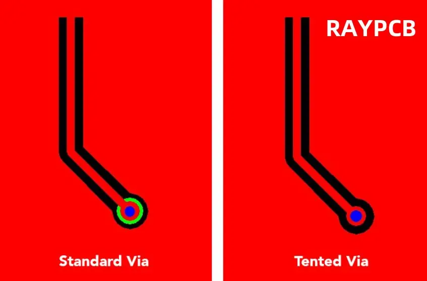
- Untented Vias: Remain exposed for potential post-assembly access
- Tented Vias: Fully encapsulated by soldermask for protection
What is PCB Via Tenting?
Before we dive into via tenting, it’s important to understand what a via is in PCB design. A via is a small hole drilled through a PCB that is plated with conductive material, allowing electrical connections between different layers of the board. Vias play a crucial role in routing signals and power in multi-layer PCBs.
Via tenting is a process used in PCB manufacturing to cover or “tent” over vias with a layer of solder mask material. This technique is employed to protect the vias from environmental factors and to improve the overall reliability and appearance of the PCB.
Read more about:
What Does it Mean to Tent a Via?
When we talk about tenting a via, we’re referring to the process of covering the via hole with solder mask material. This creates a protective barrier over the via, effectively “sealing” it from the external environment. The solder mask, typically green in color (though other colors are available), is applied during the PCB manufacturing process.
Tenting a via involves several steps:
- Drilling the via hole
- Plating the via with conductive material
- Applying solder mask over the entire board
- Ensuring the solder mask covers the via opening
The result is a smooth surface over the via, with the hole underneath protected from external elements.
The Advantages of Tenting Via
Via tenting offers several significant benefits in PCB design and manufacturing:
1. Enhanced Protection
Tented vias are shielded from moisture, dust, and other contaminants that could potentially cause short circuits or corrosion. This protection extends the lifespan of the PCB and improves its reliability in various environmental conditions.
2. Improved Aesthetics
Tenting creates a smoother, more uniform surface on the PCB. This not only looks more professional but can also aid in the assembly process by providing a cleaner surface for component placement.
3. Solder Mask Dam
The tenting process creates a solder mask dam around surface mount pads, helping to prevent solder bridges during the reflow soldering process. This can significantly improve the quality and reliability of solder joints.
4. Reduced Manufacturing Defects
By covering vias, tenting helps prevent solder from wicking down into the via holes during the soldering process. This reduces the likelihood of insufficient solder on component leads, which can lead to weak or faulty connections.
5. Cost Reduction
In some cases, via tenting can eliminate the need for via plugging, a more expensive process used to fill via holes. This can lead to cost savings in PCB manufacturing.
Via Tenting Vs Non Via Tenting

To fully appreciate the benefits of via tenting, it’s useful to compare it with non-tented vias:
Tented Vias:
- Protected from environmental factors
- Smoother board surface
- Reduced risk of solder wicking
- Improved aesthetics
- Potentially lower manufacturing costs
Non-Tented Vias:
- Exposed to potential contamination
- Visible holes on the board surface
- Higher risk of solder wicking during assembly
- May require additional processes like via plugging
- Useful for test points or when heat dissipation is needed
The choice between tented and non-tented vias depends on the specific requirements of your PCB design and its intended application.
11 PCB Design Rules for Via Tenting
To ensure successful via tenting in your PCB design, consider the following rules:
1. Size Matters
The size of the via is crucial for successful tenting. Generally, vias with a diameter of 0.3mm (12 mils) or less are easier to tent reliably.
2. Consider Via Location
Vias placed too close to pads or other board features may be difficult to tent effectively. Maintain adequate spacing between vias and other elements.
3. Use Appropriate Solder Mask Thickness
The thickness of the solder mask layer is critical. It should be thick enough to cover the via opening but not so thick that it interferes with other aspects of the board design.
4. Account for Manufacturing Tolerances
Remember that manufacturing processes have tolerances. Design with some margin to ensure successful tenting even with slight variations in production.
5. Specify Tenting in Design Files
Clearly indicate which vias should be tented in your design files and manufacturing notes to avoid confusion.
6. Consider Signal Integrity
For high-speed designs, consider the impact of tenting on signal integrity. In some cases, exposed vias may be necessary for optimal performance.
7. Balance Tenting with Heat Dissipation
In designs where heat dissipation is crucial, selective non-tenting of vias may be necessary. Balance protection with thermal management needs.
8. Evaluate Stackup Impact
Consider how via tenting might affect your overall PCB stackup, especially in terms of board thickness and layer-to-layer spacing.
9. Plan for Testing
If in-circuit testing is part of your quality control process, ensure that tented vias don’t interfere with necessary test points.
10. Consider Impedance Control
For controlled impedance designs, factor in how via tenting might affect impedance calculations and performance.
11. Document Special Requirements
If your design requires specific tenting approaches or materials, clearly document these requirements for your PCB manufacturer.
Via Tenting Types

There are several types of via tenting that can be employed depending on the specific needs of your PCB design:
1. Full Tenting
In this approach, the via is completely covered by solder mask on both sides of the board. This offers maximum protection but may not be suitable for all designs.
2. Partial Tenting
Partial tenting involves covering the via on one side of the board while leaving it exposed on the other. This can be useful when some level of access to the via is needed.
3. Selective Tenting
This method involves tenting some vias while leaving others exposed, based on the specific requirements of different areas of the PCB.
4. Epoxy Tenting
In some cases, epoxy may be used instead of solder mask for tenting. This can provide enhanced protection in harsh environments.
Via Tenting Materials and Methods

The choice of materials and methods for via tenting can significantly impact the performance and reliability of your PCB:
Solder Mask
The most common material used for via tenting is solder mask. It’s typically applied as a liquid and then cured, creating a durable, protective layer.
Epoxy
For more demanding applications, epoxy-based materials may be used. These can offer superior protection against moisture and chemicals.
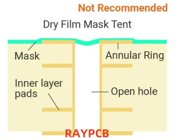
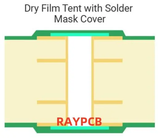
Dry Film Solder Mask
Some manufacturers use dry film solder mask for tenting. This can provide more consistent coverage, especially for smaller vias.
Tenting Tape
In some prototyping or low-volume production scenarios, special tenting tape may be used to cover vias.
PCB Via Tenting Fabrication Process
The via tenting process is integrated into the overall PCB manufacturing workflow:
- Design and File Preparation: The PCB design, including via locations and tenting requirements, is finalized and prepared for manufacturing.
- Via Drilling: Holes for vias are drilled according to the design specifications.
- Via Plating: The via holes are plated with conductive material to create electrical connections between layers.
- Solder Mask Application: Liquid solder mask is applied to the entire board surface.
- Tenting Process: The solder mask is allowed to flow over the via holes, creating the tenting effect.
- Curing: The board is cured, typically using UV light or heat, to harden the solder mask.
- Inspection: The board is inspected to ensure proper tenting and overall quality.
- Additional Processing: Any necessary additional steps, such as surface finishing or silkscreen printing, are completed.
By following these steps and adhering to best practices in via tenting, PCB designers and manufacturers can create high-quality, reliable circuit boards that meet the demanding requirements of modern electronic devices.
In conclusion, via tenting is a crucial aspect of PCB design and manufacturing that offers numerous benefits in terms of protection, aesthetics, and reliability. By understanding the principles, types, and best practices of via tenting, designers can make informed decisions that lead to superior PCB performance and longevity. As PCB technology continues to evolve, mastering techniques like via tenting will remain essential for creating cutting-edge electronic products.