The Rogers 4360 PCB is a 6.14 Dk, low loss hydrocarbon that features a glass reinforcement material and a ceramic filling thermoset. This offers the best equilibrium possible between processing ease and achievement.
This is denoted as CTE. This measures the rate at which the expansion of a PCB material takes place whenever it heats up. It is expressed in ppm (parts per million), which expands for every degree Celsius of heat. It is measured in PPM/oC. Anytime the material’s temperature rises higher than the Tg, there will be a rise in CTE as well.
This is denoted as k. This property tells the material’s capability to conduct heat. When the thermal conductivity is low, it means the heat transfer is low, and vice versa. This property is measured in Watts/meter Kelvin.
Glass Transition Temperature
This is denoted as Tg. This temperature is one at which the substrate changes into a deformable and soft state from the glassy rigid state. It is measured in degrees Celsius.
Decomposition Temperature
This temperature is where the material will decompose chemically. It is also measured in degrees Celsius.
This value is the ratio of the electric permeability of the material to that of free spaces.
Dissipation factor (Df) or Loss Tangent
This value is the tan of the phase angle, which is between the reactive and resistive currents of the dielectric. There is an increase in dielectric loss whenever the dissipation factor increases. A dissipation factor that is low delivers fast substrates, while dissipation factors that are large deliver slow substrates.
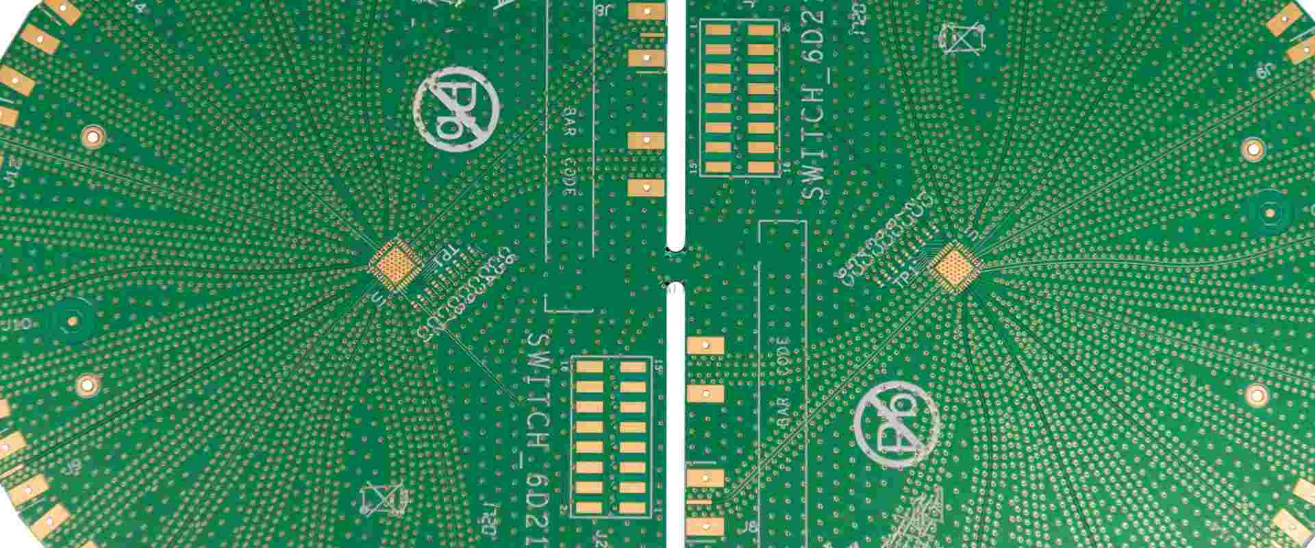
Sure, it is possible to form a multilayer PCB after applying some RO 4360 together. The RO 4360 provides a low level of interference and high signal integrity. In every multilayer PCBs, there must be at least three conductive layers.
The production of multilayer PCB requires the lamination of the core items and prepeg’s alternating layers at high pressure and temperature. This makes sure that no air stays between the layers, and also ensures that these layers are held by resin.
What to do when Choosing the Rogers 4360
There are things to do before choosing rogers 4360, these include:
Make sure there is a match in the Coefficient of Thermal Expansion: The coefficient of thermal expansion is a very important thermal trait when dealing with substrates. Difference in the CTE rates tells that during fabrication, they will expand at different rates.
Choose Materials Having Similar Dielectric constant: Make sure you go for substrates having identical dielectric constant.
Go for Tight and Flat Substrate Weaves: Doing this makes it great for high-speed and high-frequency usages. Also, it offers an even distribution of the dielectric constant.
Choose Low Moisture Absorption Materials: Moisture absorption has to do with the PCB material’s resistance when it is submerged in water. There will be an increase in the PCBs weight as the material gets absorbed in water and it falls within the range of 0.01 and 0.02%.
Avoid Using FR-4 for Applications Requiring High Frequency: Don’t do this, because their dielectric loss is high. In addition, there is a sharp Dk when compared to the frequency response curve.
Rogers ro4360 comes with different uses, which includes:
Automotive
Modern vehicles feature many electrical components that ensure their functionality. Some of these applications are:
Media devices
Navigation systems i.e. satellites
Proximity systems such as sensors which notifies the driver anytime objects come near
Control systems such as power supply, fuel generators, etc.
Consumer Electronics
Millions of people depend so much on these devices. They include:
Computers such as laptops, desktops, satellite navigation devices, etc.
Home appliances such as coffee makers, microwaves, alarm clocks, etc
Communication devices like smartwatches, smartphones, radios, etc.
Entertainment systems like TV sets, DVD players, stereos, etc.
Industrial Application
The RO 4360 are useful in their manufacturing firms and production lines. These include:
Industrial equipment such as assembly machines, ramps, etc.
Power equipment such as inverters, power supplies, power distribution devices, etc
Measuring equipment, which controls pressure, temperature, and other parameters for manufacturing
Medical Application
It is relevant in applications such as:
Monitors detecting heart rate, sugar level, blood pressure, etc.
Scanners such as CT scans, X-ray machines, ultrasonic scans, etc.
Medical devices such as compressors, electronic microscopes, etc
Conclusion
The Rogers 4360 is a very reliable material with lots of great benefits. It can be fabricated easily and permits an effective supply chain. Its design is flexible and works fine with plated through-hole. Also, its material is environmentally friendly, and it is affordable, compared to other PTFE products.
The Rogers RO3010 laminates are products with competitive prices having great electrical and mechanical stability. With this stability, the broadband components’ design is simplified, allowing the utilization of materials in different applications over a wide range of frequencies. The characteristics of this material make the RO3010 laminates great for circuit miniaturization.
The design of this circuit board has to do with the microwave circuit’s electrical performance requirements. This is manufactured from high-frequency high-quality insulting and laminated material. It possesses great mechanical strength and high signal anti-interference ability.
This PTFE ceramic-filled laminate/composite can be utilized in applications reaching 77 GHz. At room temperature, it has a dielectric constant of 11.20, which can reach 40 GHz. Asides from this, its dissipation factor at 10 GHz is 0.0022, which is suitable for patch antennas, GPS antennas, direct satellite applications, and automotive radars.
Its mechanical properties are usually consistent no matter the dielectric constant chosen. This allows the development of multi-layer board designs by the designer. These multi-layer board designs utilize different materials for dielectric constant for individual layers, without facing reliability or warpage problems.
Its expansion coefficient is similar to that of copper. This allows the material to show great dimensional stability, with etch shrinkage. The RO3010 can be transformed into PCBs (Printed Circuit Boards) making use of standard processing techniques of PTFE circuits, with minimal modifications.
The Roger RO3010 has a dielectric constant of 11 and a dissipation factor of 0.0022. It also has a Td of 500 °C. Its flammability rating is UL 94-VO, which indicates that PCB material specimens shouldn’t burn with combustion for over 10 seconds. Its peel strength and water absorption values are 9.4 lb/in and <0.1%. Also its thermal coefficient and thermal conductivity values are 11 ppm/°C and 0.79 W/m/K respectively.
Great for use with board designs having multi-layers
Material has dimensional stability and has an expansion coefficient similar to that of copper. This permits more surface mounted assemblies. Also, this makes them great for applications that are sensitive to changes in temperature. With this, great dimensional stability is ensured.
Dielectric constant is stable versus frequency and temperature. This makes the roger RO3010 great for microstrip patch antennas, voltage-controlled antennas, and band pass filters.
Its mechanical properties are uniform for a range of dielectric constants. This makes them ideal for board designs with multi-layers for a range of dielectric constants. Also, suitable when used with epoxy glass board hybrid designs with multiple layers.
Low dielectric loss. This laminate can be utilized in applications up to 77GHz.
Applications of Roger RO3010
Antenna Systems
The Rogers RO3010 is designed to meet the challenges antenna designers face, which includes the high requirements of antenna systems used by the military as well as automotiveradar systems that are advanced. These solutions provide different dielectric products for feed networks, antennas, radiating elements, and phased arrays.
Patch Antennas
At any frequency, Rogers RO3010 provides different thicknesses and dielectric constant to ensure space and bandwidth requirements. These options also include the stability of the dielectric constant over temperature and thickness control for conformal antennas and thick antenna structures.
Phased Array
For phased-array antennas, before going ahead to choose circuit laminate materials for them, some key designs to consider include stable and low loss performance and dielectric constant uniformity. The advanced materials used here are specifically designed to be used in antenna fabrication, high speed and multilayer RF digital boards.
Conformal Antennas
The Roger RO3010 is also great for non-planar uses, and has been successful in different conformal antenna applications involving simple curvatures, which includes small diameter cylinders.
Active Electronically Scanned Array
Designs made up of multilayer structures that are complex in nature are usually common here. The Roger RO3010 controls mechanical and electrical properties to ensure phase accuracy over temperature and frequency. High thermal conductivity and low CTE ensures more reliability compared to power cycling.
The innovative materials used in Rogers RO3010 ensure advancement in microwave and RF technology and great functionality of the microwave communications systems. Regarding complex microwave applications, laminates with high-frequency won’t just deliver low loss, they also deliver well-controlled dielectric constant. Most RF subsystem applications reveal that controlling the dielectric constant for that material may be very critical, just like controlling the substrate thickness.
Rogers has been well-known for providing materials for advanced and RF microwave power amplifiers and the Rogers RO3010 is not left out. High thermal conductivity, great long-term aging features under heat, stability over temperature, and low loss, offer the highest power output and efficiency possible.
Low Noise Receivers and Amplifiers
There’s a need for low noise amplifiers to function efficiently across different environmental conditions, and this is where the Rogers RO3010 comes in. The low loss, as well as the thermally-stable RF materials goes a long way in achieving the best performance even in environments that are very demanding.
Control Circuitry of Digital Communications
For advanced systems of microwave communications, precision circuitry becomes important in maintaining the high-speed signals’ integrity. The low loss materials of the Rogers 3010 supports lower crosstalk, higher data rates, and faster switching. The design of the RO3010’s composites is for skew reduction via using relatively low fiberglass and flat glass content.
The Roger RO3010 is useful for Wifi and handheld device cellular antennas. This is because most handheld devices have WiFi and cellular antennas. This ensures even the smallest of mobile devices has access to the internet through local WiFi access points or global mobile networks. It also has the ability to convert the device into a hotspot. With high performance antennas, you are sure to have reliable connectivity, as well as access to different global frequencies and wireless standards.
Conclusion
The Rogers RO3010 laminates have great electrical and mechanical stability. This ensures the simplifying of the broadband components’ design, allowing the utilization of materials in different applications over a wide range of frequencies. This circuit board is manufactured from high-frequency high-quality insulting and laminated material. Its mechanical properties are usually consistent no matter the dielectric constant chosen. Its expansion coefficient is similar to that of copper. This allows the material to show great dimensional stability, with etch shrinkage.
China has become a leading hub globally for electronics manufacturing services including prototype engineering and low volume production. The availability of skilled engineers, advanced manufacturing infrastructure and competitive costs has attracted many multinational OEMs, startups and design houses to source electronics prototyping in China.
This article profiles the top 12 electronic prototype manufacturers in China who deliver advanced capabilities, quality and rapid turnaround for NPI (new product introduction) engineering.
1. RayMing Technology
RayMing is an ISO 13485 and ISO 9001 certified company focused on fast turnkey prototyping of electronic devices. With over 200 engineers and three manufacturing facilities, they deliver advanced capabilities across PCB design, component engineering, enclosure design, firmware development and testing services.
StarLink provides rapid prototyping and electronics engineering services to help companies launch products faster. With over 500 engineers and 14 years of experience supporting startups, they deliver functional prototypes meeting quality and reliability needs.
Location: Zhuhai, China
Services:
PCB Development
Mechanical Engineering
Prototype Manufacturing
Product Testing
Industries Served:
Consumer Electronics
Automotive Electronics
Industrial Electronics
Medical Electronics
Customers: Startups, medium/large companies in North America and Europe
Key Differentiators:
Rapid prototype delivery in 7-15 days
One stop engineering capabilities
Scalable volume production
Strong focus on quality
Certifications: ISO 9001, ISO 14001, QC 080000
3. Wispro Technology
Wispro provides electronic product design, prototyping and manufacturing services. With 700+ employees, they deliver high quality prototypes and low volume production using advanced technologies.
28 years of experience supporting electronics OEMs
High quality prototypes with quick turnaround
Seamless transition to production
Rigorous quality systems
Certifications: ISO 9001, ISO 14001, ISO 13485
4. Libing Technology
Libing provides professional one-stop engineering services focused on electronic product design and manufacturing. With over 200 employees and 10 years of experience, they deliver reliable high-tech solutions.
Advanced Assembly provides rapid prototyping of electronic devices with a focus on assembling and testing prototypes. They leverage an international supply chain to procure components and build prototypes.
OurPCB provides fast PCB prototyping as well as electronics assembly. They have instant online quoting and order placement for PCB fabrication and assembly with flexible quantity.
Location: Shenzhen, China
Services:
24 Hour PCB Prototypes
SMT Assembly
PCB Component Procurement
Functional Prototype Building
Industries Served:
Consumer Electronics Makers
Maker Community
Small Businesses
Education and R&D
Customers: Startups, makers, hackers, students and electronics enthusiasts globally
JZJ PCB provides advanced PCB prototype services as well as electronics manufacturing. They have 16 years of experience focused on meeting prototyping needs for innovators worldwide.
Customers: Startups, makers, and electronics innovators globally
Key Differentiators:
High quality multilayer PCB prototypes
Flexible order quantities
Design for manufacturing services
Seamless transfer to production
Certifications: ISO 9001, ISO 14001, UL
8. Wellpcb Technology
Wellpcb offers advanced PCB prototyping capabilities using high end manufacturing equipment. They provide engineering services to support all phases of electronic product development.
Amitron delivers electronics engineering design including PCB layout, simulation, mechanical design and prototyping services to customers globally.
Location: Shenzhen, China
Services:
PCB Design Services
PCB Simulation and Analysis
Electronic Product Design
Mechanical Engineering Design
Prototype Fabrication
Industries Served:
Industrial Equipment
Consumer Electronics
Automotive
Medical Devices
Customers: Small and mid-sized electronics companies, startups, makers
Key Differentiators:
Advanced engineering capabilities and expertise
Strong focus on electronics reliability
Experience supporting a wide range of industries
End-to-end product development services
Certifications: ISO 9001
10. PCB Masters
PCB Masters provides professional engineering support for PCB prototyping along with design for manufacturing analysis. Their capabilities support faster development of electronic devices.
JingHongYiDa provides specialized electronics engineering services focused on supporting product design and prototyping. Their capabilities help accelerate time-to-market.
Limei provides specialized electronics manufacturing services focused on supporting engineering teams with PCB fabrication and assembly. Their capabilities help accelerate prototyping.
China offers a wide range of capable electronics manufacturing services companies to partner with for engineering and prototyping new electronic devices. They provide advanced expertise, rapid turnaround, and competitive costs to help innovators accelerate product development. With stringent quality systems, international sourcing and experience transitioning to production, they enable streamlined new product introduction. Global OEMs, startups and entrepreneurs are leveraging these expert Chinese prototyping partners to bring their electronics innovations to market faster.
Frequently Asked Questions
Q1: What are some of the benefits of prototyping electronics in China?
Some key benefits are:
Access to skilled, low cost engineering talent
Mature component supply chains
Advanced manufacturing technologies
Ability to scale to high volume production
Cultural understanding of local Chinese market
Cost savings compared to domestic US or Europe prototyping
Convenient time zones for communication
Q2: What due diligence should be done before selecting an electronics prototyping partner in China?
Important factors to consider in selection process:
Review their design capabilities, expertise and past projects
Evaluate their quality certifications and processes
Ensure they have good security and IP protection
Check lead times, minimum order quantities
Validate responsive communication channels
Request customer references to check satisfaction
Review their component sourcing abilities
Audit their manufacturing setup if possible
Align on project requirements like documentation, DFM, inspection testing needed
Prepreg, also referred to as pre-impregnated composite fibers, is a key material used in the manufacture of multilayer printed circuit boards (PCBs). It is a fibrous reinforcement that has been pre-impregnated with a resin system prior to laminating PCB layers together.
Prepregs provide electrical isolation between the conductive copper layers in a PCB while also offering mechanical stability. They impart crucial properties like dimensional stability, bond strength, heat resistance and dielectric performance. Selecting the right prepreg material is critical for the reliability of multilayer PCBs used in electronics.
This article provides an overview of PCB prepregs covering their composition, properties, types, role in the PCB fabrication process and methods for quality control testing.
Composition of PCB Prepregs
Prepregs used for PCB fabrication are generally composed of:
Fiberglass fabric reinforcement
Epoxy or other polymer resin systems
Filler particles like silica
Catalysts and accelerators
Flame retardants
Fiberglass Fabric
The fiberglass fabric provides mechanical strength and dimensional stability. Some types used are:
108, 211 fiberglass with 5-15 μm diameter fibers
Woven fabric with different weave styles
Non-woven random fiber mats
Resin System
The resin coats and bonds together the fibers. Different resin types used are:
Fillers like fused silica reduce the coefficient of thermal expansion (CTE) of the composite to match copper. They also control flow, adhesion, thermal conductivity and cost.
Other Components
Small amounts of curing agents, accelerators, flame retardants and other additives tailor the prepreg properties.
Desirable properties in prepregs for quality PCBs:
Dielectric Constant – Stable dielectric constant and low dissipation factor for high frequency performance. Values of 3.5-5 typical for glass fabric-epoxy prepregs.
Dimensional Stability – Low Z-axis shrinkage and expansion under temperature cycling to avoid via failures. Typical X-Y shrinkage < 0.5%.
Bond Strength – Strong adhesion to copper foils and between prepreg layers with good resistance to delamination. Bond strength > 2.5 N/mm.
Decomposition Temperature – High Td above 300°C indicates stable thermal performance and prevents charring issues.
Moisture Absorption – Low affinity for moisture prevents electrical leakage and reliability issues due to vapor pressures. <0.5% uptake standard.
Flow and Filler – Adequate resin flow to fill irregularities but not excessive to avoid shorts between conductors. Filler loading around 15-40%.
Flame Retardancy – High degree of flame resistance with resistance to ignition, burning and smoke generation. UL 94 V-0 rated material.
Types of PCB Prepregs
Many varieties of prepregs cater to different PCB performance requirements:
Type
Key Characteristics
FR-4 Epoxy
Most widely used. Good processability. Low cost. Temperature rating 130°C (Tg 135-155°C)
High Tg Epoxy
Tg > 170°C for higher heat resistance. Ex: BT epoxy, Allied Signal Arlon85N
PPO (Polyphenylene oxide)
Low loss and stable Dk for RF/microwave. Improved Z-axis CTE. Ex: Rogers TMM 10i
Cyanate Ester
Lowest loss, tightly controlled Dk for high freq. Ex: Taconic TacPreg CE
Prepreg is used to bond the inner copper layers into a multilayer board through lamination under heat and pressure.
2. Electrical Isolation
It provides electrical isolation between two conductive copper sheets or internal planes while still allowing conduction through drilled holes.
3. Inner Layer Core
Prepreg-copper sheets also serve as the starting cores during the layup of multilayer PCBs.
4. Serving Solder Mask
Special prepreg with photo-sensitive resin can act as the solder mask layer on outer surfaces.
5. Imparting Rigidity
The composite material lends mechanical strength and rigidity to the PCB structure.
6. Controlling Z-axis CTE
Low expansion prepregs control growth along thickness to avoid reliability issues.
7. Providing Heat Resistance
High Tg prepregs allow PCB operation at elevated temperatures.
8. Establishing Dielectric Constant
The resin-fiber matrix governs the dielectric constant of the insulating PCB layers.
PCB Prepreg Handling Considerations
To maintain quality, prepregs require careful handling:
Prepregs are supplied sealed in polythene bags to prevent moisture absorption. Unused prepreg should be resealed immediately.
Storage temperature should be 18-25°C. Freezing conditions can ruin the material while excessive heat can cause partial curing.
Shelf life is typically 1 year at 23°C. Prepregs should be used on a FIFO basis before expiry.
Allow refrigerated prepreg to reach room temperature before opening to prevent moisture condensation.
Avoid excessive exposure to UV light which can initiate polymerization. Use under yellow light.
Use clean lint-free gloves when handling to avoid contamination of the tacky surfaces.
Proper prepreg handling as per manufacturer guidelines ensures consistent performance.
PCB Prepreg Testing
Some key tests carried out on prepreg materials for quality control are:
Resin Flow Testing
Resin viscosity measured at standard temperature and pressure
Tested after partial curing for specified duration
Ensure adequate but controlled flow during lamination
Gel Time Test
Monitoring resin polymerization at set temperature
Inflection point taken as gel time
Checks adequate processing window before curing
Differential Scanning Calorimetry
Monitors heat flow versus temperature to detect transitions
Gives resin glass transition temperature, cure peaks
Indicates degree of curing with heat ramps
Dielectric Constant
Measured over frequency range like 10 MHz – 10 GHz
Indicates electrical insulation capability
Stable value desired through frequency spectrum
Flammability Testing
UL 94 vertical burning test rating for flammability
High priority for safety critical PCB applications
Prepreg received from supplier is also tested before PCB usage.
Conclusion
Prepreg forms the fundamental dielectric building block of multilayer PCBs that electrically isolates the conductive layers while also imparting mechanical strength. The composition of the resin, fabric reinforcement and fillers that make up prepreg governs the thermal, electrical and reliability performance of the PCB. With the diversity of prepreg types available, PCB manufacturers can select the optimal material suited for their performance requirements and process compatibility. Strict handling and quality control measures for prepreg also minimize variability and ensure consistent results during PCB fabrication. As PCBs become thinner and operate at higher frequencies and temperatures, engineering the prepreg materials is critical for enabling their miniaturization and reliability.
Frequently Asked Questions
Q1. How does prepreg material selection influence the fabrication process of multilayer PCBs?
Some ways prepreg properties affect multilayer PCB fabrication are:
Flow viscosity during lamination cycle time and temperature
Tg impacts the curing required and potential rework
Low thermal expansion suits large area boards
High filler suits complex topographies
Adhesion levels affect press parameters
Moisture sensitivity influences handling
Dielectric properties affect impedance control
Q2. What are some troubleshooting tips for issues with PCB prepreg?
Troubleshooting tips for prepreg related PCB issues:
Delamination or blistering – Poor adhesion, high moisture absorption
Cracking or crazing – Excessive resin flow, filler settlement
Poor dimensional stability – High Z-axis CTE material
Wicking or shorts – Insufficient resin viscosity
High dielectric constant – Incompatible resin system
Poor heat resistance – Low Tg material used
So proper prepreg selection, handling and process controls are vital.
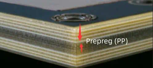
Difference between PCB Core and Prepreg Materials
Prepreg Core is the isolating material of the PCB, often referred to as before laminating. Manufacturers mostly use Prepreg as a binding substance. Not just that, experts also employ it as a multifunctional PCB inner conduction material. Thus, once the user laminates the Prepreg & extrudes the half-healed epoxy, it solidifies and runs and binds the multilayer panels together to create a dependable insulator.
When the distinction between both Core and Prepreg is evident, what specific property should you use? When plate, etching, and drying, how do crucial electrical characteristics change? As more manufacturers are aware of the work at GHz frequency range, these principles are vital to size traces of these materials appropriately and prevent difficult signal integrity difficulties.
WHAT IS PREPREG MATERIAL?
Prereg PCB is a conductive substance that planners pack to provide the appropriate insulate between the copper and a core or dual Core of a PCB. Prereg is a level of isolation. Since a copper sheet and a core may be bonded, it may be called a binding material safely. Users may also customize Prereg as special insulators to their demands. A chemical technique may also be used to turn a given section of a Prereg into a conducting zone by combining appropriate catalytic substances and additives.
The PCB core is a hard foundation material coated on one or two aspects with copper. The CORE is employed in the fabrication of single-sided and two-sided boards and in the manufacture of PCBs of sharing arrangements.
The PCB center consists of the FR4 elements of titanium epoxy laminates and copper traces. The Prereg connected the layers and the PCB core when users heated there.
Experts responded to the Core as the core panel and also to the Core of PCB production. It has a certain copper, width, and firmness of double bread. Its multilayer board is a mixture of Prereg and Core.
HOW IS PREPREG MADE?
Prepreg is a fiberglass fabric/towel coated with a resin preservative, as the name implies. The glass strands are knitted into a glass tissue. This glass fiber fabric is half-dried into material from the B-stage.
Most prepregs are substances of the B-stage. It is vital to track the volume fraction of the material used throughout the production process Prepreg, as it enables the material to be adjusted according to the demand. The number of repetitions of warp and fill affects the epoxy the glass weave can hold.
HOW WE CAN CHOOSE PREPREG MATERIAL:
Depending on the size and other needs, many kinds of prepregs are integrated into PCBs. According to its resin composition, Prepregs are compatible with standard resin (SR), mid resin (MR), or high resin (HR). The more and more resin it holds, the more costly it becomes.
CORE AND PREPREG MATERIALS:
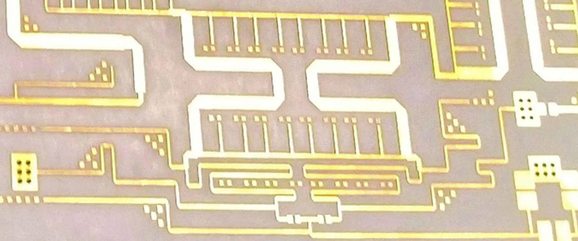
With clear structural differences in the core prepreg materials, it is critical from a circuit design perspective to get an exact value for the electrical conductivity and the return loss. If your signals have minimal growth time, you can usually get away using a user information sheet value. Once your knee and analog signals have reached the GHz range, attention must be taken with the datasheet values, particularly when modeling interconnect behavior and employing resistance-controlled routing.
The difficulty with data source numbers is that the true electrical conductivity determined is based on the test technique, geometric routing, particular frequencies, convention on the law, and the thickness of the material. John Coonrod spoke extensively about this subject in a recent interview. The fabric pattern of PCB core/prepreg components renders them inhomogeneous and anisotropic, meaning that the main material qualities change in space and various directions. This is why we get fiber weaving phenomena such as excitation of the skew and fiber cavity.
You could wonder, why should a laminate density define the material characteristics? The reason is that the important parameter characterizing the signal behavior is a useful electrical conductivity, which relies on your material’s trace size and layer thickness.
Finally, copper texture on a particular laminate is the second key characteristic to be considered. The above two studies Will present efficient dielectric constant calculations for the geometries of microstrip and strip lines without the assumption of copper ruggedness. There is, however, a straightforward linear approach to compensate for copper rawness:
Suppose you are working at really high speeds and high frequencies and want very precise connection characterization. In that case, the best choice is to produce a test coupon and utilize standard measurements to calculate the functional dielectric constant. A topology that roughly resembles your anticipated interconnection geometry should be used in your test procedure. This requires some effort at the front, but precise testing and measuring might save you needless prototype runs in the rear.
Suppose you pick from a variety of PCB core versus prepreg material, the Altium Designer. You will have access, or you may define special material characteristics for exotic substrates, to a component library that offers crucial information on various standardized materials. These capabilities enhance your efficiency and enable you to adjust your design to very particular applications.
PCB cores and coatings are comparable yet extremely distinct in certain aspects. Your Core is one or more prepreg panels crushed, hardened, and heat-cured, and the Core is covered on each side with a copper foil. The resin is injected with the prepreg material, wherein the resin is solidified but left untreated. Many companies define Prepreg as the duct tape that ties the core components together; the exposure to heat allows the resin to start binding to the next layers when 2 cores are placed at either edge of a prepreg lamellate. The solidified resin cures slowly bypass, and its resultant material characteristics approximate the core layers.
The resin substance contains a glass fabric. The production procedure for this glass fabric is quite similar to that for the fabrication of yarns. The glass fabric may be pretty narrow (e.g., 7638 prepreg) or flexible (e.g., 1081 prepreg), manufactured by the weaver. Any flaws and general yarn uniformity will decide the magnetic characteristics responsible for the scatter, loss, and fiber tissue impact of the signals in the circuit.
According to the resin amount, resin variety, and glass fabric, core PCB vs. prepreg materials may have a slightly differing refractive index. This may be a concern if boards need to be designed that match extremely exact impedances since the absorption coefficient observed on a track relies on the dielectric constants of the material resulting. Not even all prepreg and core materials are mutually compatible, and core/prepreg stacks with widely varying dialectal constants make predicting accurate dielectric constants and inefficiencies in an interconnection problematic.
Every PCB core or prepreg material has a problem with high voltage creeping and leakage current. Copper electromigration and further expansion of conductive filaments are a cause for the FR4 material creeping criteria. This difficulty drove a move to – anti (Non-DICY) in FR4 Prepreg and coatings, albeit with a want to improve the transition of the glass and breakdown temperatures. Phenolic resins offer greater breakdown and transition temperatures than DICY resins and increase isolation resistance upon complete curing.
We can interpret it this way, and The Prepreg is a PCB isolating material. Prepreg shall not be Prepreg before encapsulation, also known as Prepreg. It shall be utilized mainly as a connecting material and an isolating material for a multilayer integrated circuit board’s inner guiding pattern. After lamination, the semi-curated epoxy is ejected, starts to flow, reinforces the multilayer sheets, and produces a durable insulator.
The Core is the essential material for the production of PCB. The Core is also referred to as the core panel, which has some toughness, depth, and double copper bread. Therefore, Core and Prepreg are a mixture of the multilayer board. The distinction between the two:
PCB material prepreg and the older material is semi-solid, cardboard-like, the later hard, copper-like,
Prepreg is a sticky + dielectric, and the Core is the fundamental PCB material; two functions are entirely distinct;
The Prepreg may be curved, not bent to Core;
Prepreg is not capacitive; the copper layer between both sides of the Core is a permeable print board.
Final Thoughts
Prereg is a must and not simply a key aspect of the PCB production process when multilayer is included. Without Prereg, manufacturers will have no substance to hold the multiple layers together. The Core and Prereg are the other two elements of the PCB. This Core contains traces of copper as a substance FR4 prepreg. The Core, meanwhile, holds the PCB via Prereg.
Rogers TMM thermoset microwave materials are hydrocarbon ceramics and thermoset polymers composites specifically designed for strip-line and microstrip applications. TMM comes in various claddings and dielectric constants. TMM laminates feature some mechanical and electrical properties that make them ideal for several applications.
TMM has an excellent thermal expansion coefficient, low dielectric constant (Dk) thermal change rate, and consistent dielectric constant. TMM can offer greater specifications of copper coating. These laminates feature the properties of both PTFE microwave circuit laminates and ceramic without needing the production techniques used for these materials.
Like other laminates that need sodium napthanate treatment before undergoing electroless plating, TMM is unique as it doesn’t require such treatment. One of the most amazing properties of TMM laminates is their extremely low thermal coefficient of Dk, which is usually lower than 30 ppm/°C.
These laminates don’t soften when they pass through heat. Due to this, wire bonding of leads to circuit traces can be easily performed without experiencing substrate deformation or pad lifting. The isotropic coefficients of thermal expansion in Rogers TMM are matched to copper, allowing for high-reliability PTH and low levels of etching shrinkage.
TMM’s thermal conductivity is almost twice of ceramic or traditional PTFE laminates, enabling it to boost heat removal. These laminates are bonded to aluminum plates or brass directly or covered with electrodeposited copper foil. The substrate thickness is between 0.015” and 0.500.” The base substrate is solvents and etchants-resistant.
According to Rogers datasheet, TMM offers Dk from 3 to 14 while having a tolerance of +/ 0.0015 inches. Rogers TMM laminates come in TMM 3, TMM 4, TMM 6, and TMM 10.
Features of Rogers TMM
Rogers TMM 3 PCB
Wide range of Dks: The dielectric constants of Rogers TMM are between 3 and 13. The dielectric constants of these laminates depend on various factors like moisture content, temperature, etc. For instance TMM4 has a dielectric constant of 4.50 +/- .045 while TMM 6 has Dk of 6.0 +/- .080.
Low thermal coefficient of dielectric constant: This is one amazing property of Rogers TMM. It has a very low thermal coefficient of Dk.
Excellent thermal conductivity: Rogers TMM thermoset microwave materials have an excellent thermal conductivity which is between 0.70 and 0.76. The thermal conductivity of these materials is twice that of ceramic or traditional PTFE laminates. These laminates are a good option for engineers as they help to reduce energy consumption and facilitate heat removal.
Coefficient of thermal expansion: The Coefficient of thermal expansion (CTE) measures the rate of expansion of a material when it is heated. Rogers TMM laminates feature low CTE matched to copper, hence enabling high reliability of PTH.
Low Dissipation factor: Rogers TMM laminates’ dissipation factors are between 0.0019 and 0.0023 at 10 GHz. A low dissipation factor indicates that this material has a more efficient insulation system. TMM’s dissipation factor is low even at room temperature.
Advantages of Rogers TMM
Rogers TMM laminates are high-grade microwave materials with great electrical and mechanical properties. These materials combine the benefits of both PTFE microwave circuits and ceramic laminates.
Exceptional mechanical properties: Rogers TMM laminates resist cold and creep flow which makes them mechanically reliable and stable.
Resistant to chemical reagent: Rogers TMM laminates resist chemical reagents which help to ensure that there is no damage during the placement and production process. These microwave materials maintain their original properties after they have been exposed to chemical reagents for a specific time.
Thermosetting resin: Rogers TMM laminates are thermosetting resin that ensures good wire bonding. These materials can withstand any type of temperature, even high heat.
Moisture absorption: These laminates can survive in a humid environment. Rogers TMM can absorb moisture from its environment; hence, it is a good material for an environment with high levels of humidity.
Major Applications of Rogers TMM
Rogers TMM laminates are useful in various applications. Due to the features and benefits of these microwave materials, they are considered a suitable option in RF and microwave circuits design, production of patch antennas, power amplifiers, and chip testers.
RF and microwave circuit: Radio Frequency (RF) and microwave circuit designers are faced with a lot of challenges and Rogers TMM laminates are specifically designed to provide a solution to some of these challenges.
These laminates are commonly used in microwave circuits due to their thermal conductivity and a wide range of dielectric constants. Radio frequency and microwave engineers use Rogers TMM thermoset microwave materials to design devices that receive or transmit radio waves.
Satellite communication system: Satellite communication systems utilize radio waves to transfer signals to the antennas on the Earth. A satellite can get signals from the earth and make use of a transponder to retransmit the signals.
Since Rogers TMM is a thermoset polymer composite that features both electrical and mechanical properties it is a core component of the satellite communication system.
Patch antenna: Patch antennas are gaining popularity within the mobile phone industry since they are easy to fabricate and cost-effective. Patch antennas require high-grade microwave materials. Rogers TMM provides a wide range of Dk and thicknesses that allow designers to achieve bandwidth and space requirements.
Global positioning system antennas: Most receiver manufacturers make use of microstrip antennas. A GPS antenna receives and transfers radio signals sent by definite frequencies from GPS satellites. These frequencies are then converted into electronic signals so that GPS receivers can utilize them. Rogers TMM laminates are a vital component of these antennas.
Power amplifiers: Power amplifiers facilitate radio signals to power levels ideal for a wired transmission to the receiver. Rogers is known for offering materials for microwave power amplifiers. Rogers TMM’s dielectric constants and mechanical properties offer the maximum power output.
Conclusion
Rogers TMM is a laminate based on thermosetting polymers, hydrocarbons, and ceramics. These laminates have processing advantages when compared with some alumina filler substrates. Rogers TMM laminates are available in TMM 10, TMM6, TMM 4, etc. however, each of these laminates have their own unique but similar properties.
These microwave materials have mechanical and electrical properties that make them useful in several applications. Rogers TMM laminates are not only suitable for microstrip applications, but are also high-reliability stripline applications.
The Rogers ULTRALAM 2000 is specially designed for applications involving microstrip circuits and for high-reliability stripline. Glass fibers are usually oriented in the laminate’s X/Y plane. This orientation ensures maximum dimensional stability. It also helps in reducing etch shrinkage when registration of the circuit feature becomes critical.
The ULTRALAM 2000 material’s dielectric constant is controlled from the nominal to ±0.04. This is done within the 2.4 – 2.6 range. There is uniformity within each panel, as well as from one panel to the other. Also, the important frequency range is extended by the dissipation factor into the K-band that falls between 17 – 27 GHz.
The Rogers 2000 laminate can be machined, sheared, and cut into shape. Also, it offers great resistance to all reagents and solvents, either cold or hot, usually utilized in the plating and etching of printed circuits. Options for cladding include electrodeposited or rolled copper.
The dielectric constant of the Rogers Ultralam 2000 falls between 2.4 and 2.6. It goes in the z direction and the condition is set at 23 degrees. This means that the ratio of the ability of this material to that of free space to carry AC (alternating current) is low.
Dissipation Factor
The dissipation factor stands at 0.0022 in the z direction at 23 degrees centigrade. This factor throws more light on how the Rogers 2000 will perform when used in different environments and applications. It gives great insight into the behavior of a circuit material when there must be a reduction in signal distortion, when a loss is significant, and when there must be a preservation of signal integrity (SI).
Volume Resistivity
The Rogers 2000 has the ability to resist insulation or electricity. It has a high volume resistivity of 2.0 x 10⁷. This makes them preferable to those with low volume resistivity. With the high volume resistivity of the Rogers 2000, you can be sure that its material will not be affected by heat, cold, and moisture.
Surface Resistivity
Moisture and temperature (either high or low) can affect surface resistivity. This is why the Rogers ULTRALAM 2000 stands out with a high surface resistivity of 4.1 x 10⁷. This shows that it has a high resistance against insulation and electricity.
This refers to the voltage at which the material of the Rogers 2000 fails to prevent current flow under the application of electrical stress. The Rogers ULTRALAM 2000 has a dielectric breakdown of >50.
Arc Resistance
The Rogers ULTRALAM 2000 has an arc resistance of 185. This is the ability of this material to resist the effects of low current, high voltage, under some prescribed conditions, after it passes through the material’s surface. This resistance is seen as the total time needed to create a conductive path of the material in which the arc has carbonized.
Coefficient of Thermal Expansion
The expansion rate of Rogers 2000 falls between 15 and 200. It can be decreased or increased. This depends on the variation of the temperature on the substrate. There is an increase in this temperature when the substrate’s temperature rises above the temperature of the glass transition. There’s a difference in the coefficient of thermal expansion between the substrate and the copper layers.
Flammability Rating
The Rogers ULTRALAM 2000 has a flammability rating of UL 94-VO. This means that users of this product can be more confident and rest assured when buying it. For manufacturers of the Rogers 2000, this certification indicates that they have worked with the most appropriate safety measures, which makes them a step higher than other competitors. The UL 94 is an important factor indicating that PCB material specimens shouldn’t burn with combustion for over 10 seconds.
Copper Peel Strength
The Rogers 2000 has a great copper peel strength which ensures the bonding of dielectric materials and copper layers. The peel strength of the Rogers ULTRALAM 2000 can be tested by exposing the traces of copper with the thickness of an ounce to heat stress, chemicals, and high temperatures.
Water Absorption
The Rogers ULTRALAM 2000 has a water absorption value of 0.03%. This means it has great tendencies to withstand water exposure. Water absorption of the Rogers 2000 will affect the electric and thermal properties of the dielectric.
Flexural Strength
Rogers 2000 has a great tendency to withstand breaking, even when physical strength is impacted upon it. The flexural strength of the Rogers 2000 is measured in two ways. The first method is to exert force at the board’s center, ensuring the ends are supported. The second way is to use Young’s modulus and tensile modulus.
LAN Systems: The Rogers 2000 can be applied in local area network systems. This network for communication helps in linking computers within a few groups of buildings or just one building.
X/Y plane oriented glass fibers: This helps in improving dimensional stability. It also does well to reduce thermal expansion. This is great for applications with critical registration.
Steady electrical properties: This opposes the rate of occurrence of repeatable designs. This feature is great for broadband applications.
Great chemical resistance: It can endure chemical attacks for long periods. They have less chance of corrosion. This helps in reducing any damage to the material during assembly and fabrication processes.
Great mechanical properties: They exhibit great physical properties when forces are applied
Standard PTFE processing: With this feature, the fabrication process comes easy.
Conclusion
The Rogers 2000 are great for applications involving microstrip circuits and for high reliability stripline. They have excellent chemical resistance and great mechanical properties. They can also be applied in different areas like radar systems, LAN systems, and more. The laminate can be machined, sheared, and cut into shape, and it offers a great resistance to all reagents and solvents.
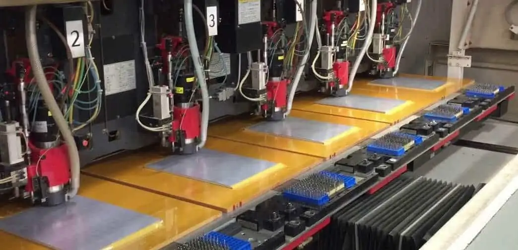
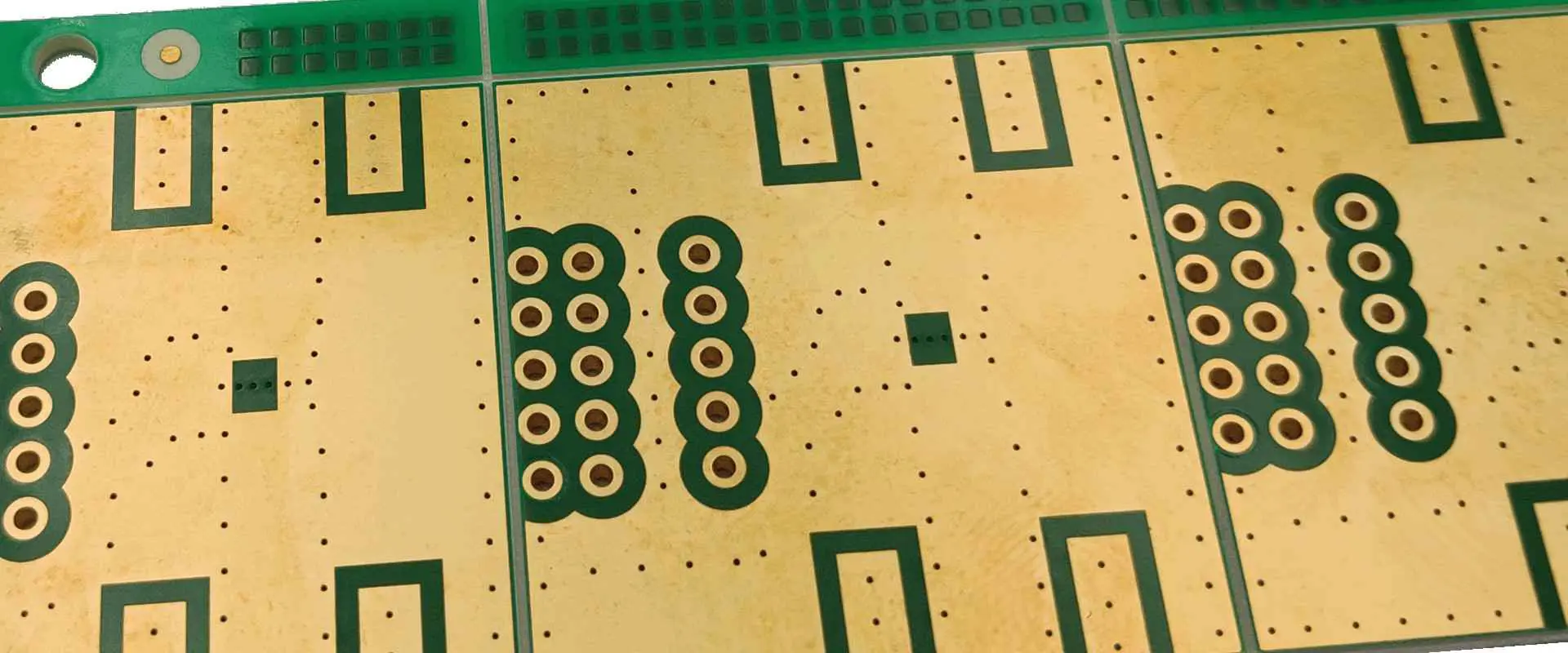
Drilling is the most costly and time-intensive stage in PCB manufacturing. Even a minor error in this process can result in significant losses, making it the most critical bottleneck in board production. PCB designers must carefully assess a manufacturer’s drilling capabilities before finalizing a design.
Drilling forms the foundation for vias and interlayer connections, enabling modern electronics to shrink from bulky, stationary devices to compact, portable systems like smartphones and ultra-thin TVs. Achieving such miniaturization demands high-precision micromachining—where drilling plays a pivotal role. Thus, the choice of drilling technology directly impacts the final product’s quality and feasibility.
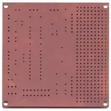
What is PCB Drilling?
PCB drilling is a fundamental step in the manufacturing of printed circuit boards. It involves creating holes in the PCB substrate to allow for the insertion of components, the formation of electrical connections between layers, and the mounting of the board to other structures. The accuracy and quality of these holes directly influence the performance and reliability of the final electronic product.
The Importance of Precision in PCB Drilling
Precision in PCB drilling is critical for several reasons:
Electrical Connectivity: Accurate hole placement ensures proper electrical connections between components and different layers of the PCB.
Component Fit: Precise drilling allows for the correct insertion and fitting of electronic components.
Board Integrity: Well-drilled holes maintain the structural integrity of the PCB, preventing cracks or delamination.
Signal Integrity: Properly drilled and plated holes help maintain signal integrity by reducing signal reflections and impedance mismatches.
PCB drilling technology has evolved significantly over the years, with two primary methods dominating the industry: mechanical drilling and laser drilling. Each technique has its advantages and is suited for different applications.
1. Mechanical Drilling
Mechanical drilling is the traditional and most widely used method for creating holes in PCBs. It involves using high-speed drill bits to physically remove material from the board.
Advantages of Mechanical Drilling:
Suitable for a wide range of hole sizes
Cost-effective for larger hole diameters
Can drill through multiple layers efficiently
Limitations of Mechanical Drilling:
Limited in producing very small hole diameters
May cause burrs or rough edges that require post-processing
Tool wear can affect precision over time
2. Laser Drilling
Laser drilling is a more advanced technique that uses focused laser beams to vaporize material and create holes in the PCB.
Advantages of Laser Drilling:
Capable of producing extremely small hole diameters
High precision and repeatability
No tool wear, resulting in consistent quality
Suitable for high-density interconnect (HDI) boards
Limitations of Laser Drilling:
Higher initial equipment cost
Limited to smaller hole diameters
May not be suitable for all PCB materials
Types of PCB Drill Holes
Understanding the different types of holes in PCB drilling is crucial for designers and manufacturers. The two main categories are:
1. Non-Plated Through Holes
Non-plated through holes (NPTH) are holes that are drilled through the PCB but do not have a conductive layer applied to their walls. These holes are typically used for:
Mounting components
Securing the PCB to an enclosure
Alignment purposes
NPTHs do not conduct electricity and are primarily used for mechanical purposes.
2. Plated Through Holes
Plated through holes (PTH) are holes that have a conductive material, usually copper, applied to their walls after drilling. PTHs serve several important functions:
Creating electrical connections between different layers of the PCB
Allowing component leads to be soldered on both sides of the board
PTHs are essential for multi-layer PCBs and complex circuit designs.
Aspects to Consider in PCB Drilling
When planning and executing PCB drilling, several crucial aspects need to be considered to ensure optimal results.
1. Aspect Ratio
The aspect ratio in PCB drilling refers to the ratio of the hole depth to its diameter. It is a critical factor that affects the drilling process and the quality of the finished hole.
Key Points about Aspect Ratio:
Higher aspect ratios (deeper holes with smaller diameters) are more challenging to drill
Typical maximum aspect ratios range from 10:1 to 15:1, depending on the drilling technology
Exceeding the recommended aspect ratio can lead to issues such as poor plating, breakage of drill bits, or incomplete hole formation
2. Drill-to-Copper
Drill-to-copper refers to the distance between the edge of a drilled hole and the nearest copper feature on the PCB. This spacing is crucial for maintaining the integrity of the board and preventing short circuits.
Importance of Drill-to-Copper Spacing:
Ensures sufficient isolation between conductive elements
Prevents damage to nearby copper features during drilling
Helps maintain the structural integrity of the PCB
Designers must adhere to minimum drill-to-copper specifications provided by manufacturers to avoid potential issues in the final product.
PCB Drilling Steps
The PCB drilling process involves several key steps, each contributing to the overall quality and precision of the finished board.
1. Positioning Holes
The first step in PCB drilling is accurately positioning the holes on the board. This process typically involves:
Using computer-aided design (CAD) software to create a precise drilling pattern
Aligning the PCB with the drilling equipment using fiducial markers or other registration methods
Ensuring that the hole positions correspond exactly with the PCB design specifications
Accurate positioning is crucial for proper component placement and electrical connectivity.
2. Insertion of the Pins
Before drilling begins, drill pins or bushings are often inserted into the drilling equipment. These pins serve several purposes:
Guide the drill bit to ensure accurate hole placement
Prevent drill bit wandering during the drilling process
Protect the PCB surface from damage caused by the drill chuck
Proper pin insertion contributes to the overall precision of the drilling process.
3. Drilling the Holes
The actual drilling process involves:
Selecting the appropriate drill bit size and type for each hole
Setting the correct spindle speed and feed rate
Executing the drilling operation according to the programmed pattern
For mechanical drilling, this step may involve:
Using entry and backer boards to minimize burr formation
Implementing peck drilling for deeper holes to improve hole quality
For laser drilling, the process includes:
Setting the laser power and pulse duration
Controlling the number of laser pulses for each hole
4. Hole Inspection
After drilling, a thorough inspection is conducted to ensure the quality of the drilled holes. This step may involve:
Visual inspection for obvious defects or misalignments
Automated optical inspection (AOI) for high-volume production
X-ray inspection for multi-layer boards to check internal layers
Measurements to verify hole diameters and positions
Any issues identified during inspection may require rework or, in some cases, scrapping of the board.
How Precise PCB Drilling Helps Minimize Costs
pcb Drill Holes
Precision in PCB drilling is not just about quality; it also plays a significant role in cost reduction. Here’s how accurate drilling contributes to cost-effectiveness:
1. Reduced Material Waste
Precise drilling minimizes errors that could lead to scrapped boards, reducing material waste and associated costs.
2. Improved Yield Rates
Higher accuracy in drilling results in fewer defects, leading to improved yield rates and lower per-unit costs.
3. Decreased Rework and Repair
Accurate drilling reduces the need for costly rework or repairs, saving time and resources in the production process.
4. Enhanced Product Reliability
Precisely drilled PCBs are less likely to fail in the field, reducing warranty claims and replacement costs.
5. Efficient Use of Board Space
Accurate drilling allows for tighter tolerances, enabling more efficient use of board space and potentially reducing overall board size and cost.
Common Drilling Issues and Their Solutions
Despite best efforts, PCB drilling can sometimes encounter issues. Understanding these problems and their solutions is crucial for maintaining quality and efficiency.
1. Drill Breakage
Issue: Drill bits breaking during the drilling process. Causes: Excessive feed rate, worn-out bits, or improper speeds. Solutions:
Regularly replace drill bits
Optimize drill speeds and feed rates
Use peck drilling for deeper holes
2. Misalignment
Issue: Holes not aligning correctly with the PCB design. Causes: Poor registration, machine calibration issues, or board movement during drilling. Solutions:
Improve board fixturing
Regularly calibrate drilling equipment
Use optical alignment systems for increased precision
3. Burr Formation
Issue: Rough edges or burrs around drilled holes. Causes: Dull drill bits, incorrect speeds, or inadequate support material. Solutions:
Use sharp, high-quality drill bits
Optimize drilling parameters
Employ entry and backer boards
4. Smear
Issue: Resin smear covering the inner layer connections in plated through-holes. Causes: Heat generated during drilling causing resin to melt and smear. Solutions:
Adjust drill speeds and feed rates
Implement proper cooling methods
Use desmear processes post-drilling
5. Nail-heading
Issue: Copper lifting around the hole entrance, resembling a nail head. Causes: Excessive heat or pressure during drilling. Solutions:
Optimize drill parameters
Use appropriate entry materials
Ensure proper maintenance of drill bits
DFM Drill Validation Tips for PCB Designers
Design for Manufacturability (DFM) is crucial in PCB design, especially when it comes to drilling. Here are some tips for PCB designers to ensure their designs are optimized for the drilling process:
1. Adhere to Minimum Hole Sizes
Follow the manufacturer’s guidelines for minimum hole sizes to ensure drillability and proper plating.
2. Consider Aspect Ratio Limitations
Design holes with aspect ratios within the capabilities of the drilling technology being used.
3. Maintain Proper Drill-to-Copper Clearances
Ensure sufficient spacing between holes and copper features to prevent short circuits and maintain board integrity.
4. Use Standard Drill Sizes When Possible
Utilizing standard drill sizes can reduce tooling costs and improve manufacturing efficiency.
5. Group Similar Hole Sizes
Grouping holes of similar sizes can minimize tool changes and improve drilling efficiency.
6. Account for Tolerance Stack-up
Consider cumulative tolerances in your design to ensure proper fit and function of the final product.
7. Provide Clear Documentation
Include detailed drilling specifications and notes in your design files to prevent misinterpretation during manufacturing.
CNC Drilling Machines and Future Technology
Computer Numerical Control (CNC) drilling machines have revolutionized PCB drilling, offering high precision and repeatability. As technology advances, we’re seeing exciting developments in PCB drilling technology:
Current CNC Drilling Technology
Modern CNC drilling machines for PCBs offer:
Multi-spindle capabilities for increased throughput
High-speed spindles (up to 250,000 RPM) for improved hole quality
Optical alignment systems for enhanced accuracy
Automated tool changers for efficiency
Future Trends in PCB Drilling
The future of PCB drilling is likely to see advancements in several areas:
Hybrid Drilling Systems: Combining mechanical and laser drilling in a single machine for versatility.
AI-Driven Optimization: Using artificial intelligence to optimize drilling parameters in real-time.
Advanced Materials: Development of new drill bit materials and coatings for improved performance and longevity.
3D Printed Electronics: As 3D printed electronics advance, new drilling techniques may emerge for these structures.
Nanotechnology: Potential applications of nanotechnology in creating ultra-small holes for next-generation electronics.
Environmental Considerations: Development of more eco-friendly drilling processes and materials.
Conclusion
Precision PCB drilling is a critical aspect of electronics manufacturing that directly impacts the quality, reliability, and cost-effectiveness of the final product. By understanding the various techniques, considerations, and best practices in PCB drilling, manufacturers can optimize their processes and produce high-quality boards consistently.
As technology continues to advance, PCB drilling will evolve to meet the demands of increasingly complex and miniaturized electronic devices. Staying informed about the latest developments in drilling technology and adhering to best practices will be crucial for PCB designers and manufacturers alike.
Whether you’re a PCB designer, a manufacturer, or simply someone interested in the intricacies of electronics production, understanding the nuances of precision PCB drilling is key to appreciating the complexity and precision that goes into every electronic device we use in our daily lives.
Rogers Corporation is known for producing high-grade laminates that feature exceptional mechanical and electrical properties. RogersULTRALAM 3850 is another type of laminate from Rogers Corporation. ULTRALAM 3850 is a high-frequency laminate that uses liquid crystalline polymer as its dielectric film.
These materials were specifically designed for both multilayer and single-layer substrate constructions. These laminates are suitable for high frequency and high-speed applications in computer data links, telecommunication networks, automotiveradar systems, and other high-grade applications.
These adhesiveless materials are known for their low dielectric constant and dielectric loss. These properties are required for designing high-speed and high-frequency products. ULTRALAM 3850 is a double-clad laminate utilized for multilayer constructions.
These laminates feature great electrical, mechanical, environmental, and thermal properties that meet the requirements of several applications. ULTRALAM 3850 can be used for multilayer constructions that feature ULTRALAM 3908 bonding film.
These laminates offer high-performance solutions that allow the production of internet connectivity, clean energy, and other technologies. The high temperature of this laminate helps it to increase the processing temperature window of the multilayer board and as well as withstand multiple solder reflow processes.
Rogers ULTRALAM 3850 is a high-frequency material available in double copper-clad. These laminates make the construction of high-speed and high-frequency multilayer circuit boards easy. They are designed to provide lasting solutions to designer’s needs.
Properties of Rogers ULTRALAM 3850
ULTRALAM 3850 has unique properties that make it an ideal option for high-performance applications like automotive radar systems, telecommunication network equipment, etc.
Stable and low dielectric constant (Dk)
ULTRALAM 3850 features a low dielectric constant of 2.9 at 10 GHz, which means it is ideal for insulating purposes. This material doesn’t break down easily when exposed to intense electric fields. Due to its low and stable Dk, it is used in several applications.
Low dissipation factor
The dissipation factor of this laminate is measured at 0.0025 at 10GHz. The dissipation factor of a laminate reveals how it performs in different environments and applications. This laminate features a low dissipation factor which makes it a good insulating material, it remains the same when exposed to any kind of temperature.
Coefficient of thermal expansion
The coefficient of thermal expansion measures how the size of a material changes when exposed to a different temperature. The CTE of ULTRALAM 3850 is 17 ppm/°C between 30.0 – 150 °C.
Dimensional stability
The dimensional stability is between -0.03% and -0.06%. This indicates that this laminate will maintain its original dimensions when exposed to various environmental conditions.
Low moisture absorption
Rogers ULTRALAM 3850 laminates can withstand a humid environment. This material has moisture absorption of 0.004 at 23°C.
Due to the mechanical and electrical properties of ULTRALAM 3850, these materials are used in high-frequency applications.
Excellent thickness uniformity: This liquid crystalline polymeric material offers exceptional thickness uniformity that ensures maximum signal integrity.
Stable electrical properties: These laminates feature stable and reliable electrical properties. Rogers ULTRALAM 3850 can conduct electrical current which makes them well suited for applications such as telecommunication networks, radar systems, etc.
Flame resistant: These laminates offer fire resistance in severe conditions. ULTRALAM 3850 doesn’t melt when exposed to severe heat. These laminates feature flame-resistant properties.
High chemical resistance: ULTRALAM 3850 materials are resistant to chemical reagents. These polymeric materials have high chemical resistance, hence, can resist chemical attack. Due to their high chemical resistance, they are corrosion-resistant. ULTRALAM 3850 chemical resistance is measured at 98.7%.
Other benefits include:
Easily bends for flexible and conformal applications
Provides design flexibility and optimizes circuit density needs
Enables utilization of thinner dielectric layer with low signal distortion
Maintains stable dimensional, mechanical, and electrical properties in a moist environment
ULTRALAM 3850 laminates are recommended for high-frequency applications. These laminates are used in RF devices, telecommunication network tools, etc.
Base station antennas: Base station antennas offer cellular connectivity to users. These antennas are utilized in covering multiple frequency bands or single frequency bands. Rogers ULTRALAM 3850 laminate is one of the major components of base station antennas.
Military satellites and radar sensors: ULTRALAM 3850 is a polymeric material essential for designing devices like military satellites and radar sensors. Radar sensors change microwave echo signals to electrical signals.
While military satellites can see things that are larger on the ground, radar sensors can determine the speed of an object along with its direction. Due to Rogers ULTRALAM 3850 properties, this laminate is a go-to option for automotive radar sensor designers.
Chip packaging: Chip packaging, also known as Integrated Circuit (IC) packaging requires the use of high speed and high-frequency materials like Rogers ULTRALAM 3850. These laminates can withstand a high temperature, which makes them well suited for any environmental condition. Chip packaging plays a vital role in the electronics industry.
Micro-electromechanical systems (MEMs): The micro-electromechanical systems feature both electronic and mechanical components. MEMs are regarded as the framework of new electronics and ULTRALAM 3850 are a core part of these systems. This material features properties that meet the increasing demands of MEMs designers.
Handheld and RF devices: Rogers ULTRALAM 3850 circuit materials are required in designing handheld and radio frequency devices. Laminates with stable electrical, dimensional, and mechanical properties meet the needs of radio frequency devices.
RF helps to send and receive radio signals between two devices. RF is needed in radar systems, remote control, television broadcasting, etc. ULTRALAM 3850 laminates have thickness uniformity that helps to achieve optimal signal integrity.
Conclusion
Rogers ULTRALAM 3850 circuit material utilizes LCP as its dielectric film which makes it unique. This material can be combined with ULTRALAM 3908 films to design adhesiveless multi-layer circuit constructions. Due to its low dielectric constant and low dielectric loss, this laminate is suitable in applications that require high frequency.
This laminate also features other exceptional properties which are required for high-temperature and high-speed products. These materials also feature copper-clad and offer high-frequency solutions to designers’ needs. ULTRALAM 3850 is a widely used and recommended laminate for several high-frequency applications.
Introduction to Electronics Manufacturing in India
The electronics manufacturing industry in India has seen rapid growth over the past decade, driven by rising domestic demand and government initiatives like the National Policy on Electronics. India is now the world’s second largest manufacturer of mobile phones and continues to attract investments from global electronics giants.
Some key facts about electronics manufacturing in India:
Market size was $67 billion in 2021 and is projected to reach $300 billion by 2025
Mobile phone manufacturing has grown from 2 million units in 2014 to about 300 million units in 2021
Laptop and tablet production has gone up from 3 million units in 2014 to 14 million units in 2020
Exports of electronics have risen from $5.8 billion in 2014-15 to $15 billion in 2020-21
Share of domestic value addition in electronics manufacturing increased from 10-15% in 2014 to 25% in 2021
The government has introduced several schemes like the Modified Special Incentive Package Scheme (MSIPS), Electronics Manufacturing Clusters (EMC) and the Production Linked Incentive (PLI) scheme to boost electronics manufacturing. Major global players like Samsung, Apple, Xiaomi, LG, Bosch, Foxconn, Flextronics and Wistron have either set up or expanded manufacturing facilities in India.
This article profiles the top 20 electronics manufacturing companies in India including details on their manufacturing capabilities, main products, investments, and recent developments.
Manufacturing locations: Noida (UP) Sriperumbudur & Chennai (TN)
Products: Smartphones, Smart TVs, refrigerators, washing machines, air conditioners
Investment: Over $1 billion in India manufacturing till date
Key info: World’s leading mobile phone and TV manufacturer. Setup world’s largest mobile factory in Noida in 2018. Employs over 70,000 people in India.
2. LG Electronics
Headquarters: Seoul, South Korea
Founded: 1958
India presence: 1997
Manufacturing locations: Greater Noida (UP), Ranjangaon (Maharashtra), Chennai (Tamil Nadu)
Key info: Leading fiber optic cable manufacturer. Exports to over 50 countries.
20. Centum Electronics
Headquarters: Bengaluru, India
Founded: 1993
Manufacturing locations: Bengaluru (Karnataka)
Products: Industrial electronics, space & defense electronics
Investment: ₹225 crore in facility expansion
Key info: Leading provider of electronics manufacturing services and solutions.
Key Factors Driving Growth of Electronics Manufacturing in India
Some of the key factors that have catalyzed the growth of electronics manufacturing in India include:
1. Rising domestic demand: India’s consumer market has seen rapid growth driven by a young population, growing disposable incomes and smartphone penetration. This has created a massive domestic demand for electronic products.
2. Government incentives: Schemes like Modified Special Incentive Package Scheme (MSIPS) and Electronics Manufacturing Clusters (EMC) have attracted global manufacturers by offering subsidies and tax benefits. The Production Linked Incentive (PLI) scheme provides incentives on incremental sales from goods manufactured in India.
3. Infrastructure development: Development of industrial clusters and corridors like the Delhi-Mumbai Industrial Corridor has enabled the creation of specialized manufacturing hubs with connectivity and logistics support.
4. Favorable policies: Progressive reforms and policies like digital India, Make in India, National Policy on Electronics have underscored India’s attractiveness as a manufacturing destination. The ease of doing business has improved significantly.
5. Supply chain ecosystems: Availability of component suppliers, ancillary units, raw material sources is enabling manufacturers to expand their production capacity in India.
6. Strategic location: India’s close proximity to key South East Asian markets, ports connectivity and free trade agreements make it an efficient export manufacturing base.
7. Skilled workforce: India has a cost-competitive skilled workforce including engineers, technicians and IT professionals that supports electronics manufacturing.
PLI scheme to incentivize exports. Target to produce 1 billion mobiles by 2025
Rising domestic demand, new product launches and exports to drive growth
Consumer Electronics
Television production reached 13 million units in 2019 with top brands manufacturing locally
Smart TV penetration expected to rise from 10% to 40% by 2025
Refrigerator production at 13 million units, 75% for domestic market
Logistics and distribution infrastructure improving penetration in smaller cities
Eco-system of component suppliers aiding local value addition
IT Hardware
Laptop and tablet production increased from 3 million units in 2014 to 14 million units in 2020
Server manufacturing has commenced in India with global majors setting up facilities
PLI scheme approved for IT hardware manufacturing
Emerging as a component hub – capacitors, printed circuit boards etc
Focus on exports especially for servers, PCs, tablets, mobile phone parts
LED Lighting
India is 5th largest producer of LED lights globally with capacity of 1 billion units
‘Make in India’ and UJALA scheme have bolstered local production and adoption
100% FDI allowed through automatic route
Electronics component clusters to aid LED manufacturing
Rising exports along with domestic market expected to drive growth
Automotive Electronics
Key products include batteries, sensors, displays, infotainment systems
Major manufacturers: Motherson Sumi, FCC Rotek, Spark Minda, Bosch India
Local value addition levels expected to rise from 15% currently to over 50%
Design and testing capabilities being enhanced
Connected mobility, EVs to drive growth for auto electronics
Industrial Electronics
Linear technologies, process control equipment, automation solutions key areas
Leading players are Honeywell, Fuji Electric, Hitachi Hi-Rel Power Electronics
Make in India boosting indigenization and local manufacturing
Increased application in infrastructure projects, energy, transportation sectors
Exports potential especially in Middle East, South East Asia regions
Strategic Electronics
High investment outlay to build domestic defense, space capabilities
DRDO labs and defense PSUs developing specialized strategic electronics tech
ISRO indigenizing satellite technology and space electronics
Policy reforms and FDI liberalization to boost private sector participation
Focus on achieving self-reliance in defense and space electronics
Key Clusters for Electronics Manufacturing Growth
India offers multiple location advantages for electronics manufacturing spanning across different states and industrial clusters:
State/Cluster
Key Companies & Products
Infrastructure & Incentives
Andhra Pradesh – Sri City
Foxconn, Xiaomi, Nokia, Huawei
– Multi-product SEZ with ready infrastructure
Mobile phones, telecom equipment
– State incentives for mega projects
Karnataka – Bangalore, Mysore
Bosch, Siemens, Tejas Networks
– Engineering talent and R&D ecosystem
Telecom, medical, industrial electronics
– Aerospace SEZs in Bangalore, Mysore
Tamil Nadu – Chennai, Sriperumbudur
Flextronics, Foxconn, Dell, Nokia, Samsung
– Electronic hardware clusters
Mobile phones, Telecom equipment, PCs
– Port connectivity & multi-product SEZs
Uttar Pradesh – Noida, Greater Noida
Samsung, LG, Dixon Technologies
– Operational metro, proximity to Delhi
Mobile phones, Consumer electronics
– State incentives for mega projects
Haryana – Gurgaon, Manesar
VVDN Technologies, SFO Technologies
– Logistics hub with connectivity to Delhi
Servers, mobile components
– Ready infrastructure in industrial estates
Punjab – Mohali
Infosys, Quark, Acius
– IT infrastructure, engineering talent pool
Electronics system design
– Incentives for IT investments
Opportunities for Further Growth
Some of the focus areas that can catalyze the next phase of growth for electronics manufacturing in India:
Exports: Tapping global markets through incentives for exports, participation in global supply chains and FTA utilization
Defense & space: Achieving self-reliance in defense electronics, space electronics through R&D and private sector participation
R&D and Innovation: Strengthening R&D efforts in futuristic technologies like AI, robotics, IoT, EVs
SME integration: Developing ancillaries and component manufacturing through SME integration and hand-holding
Skilling: Scaling up technical institutes to create specialized manpower in ESDM across states
Clusters: Developing state-of-the-art clusters with infrastructure, testing facilities and common facilities
Investor outreach: Attracting right investors through investor summits, ease of doing business reforms
Electronics value chain: Boosting local value addition across the ESDM value chain from raw materials to components to finished goods
Quality standards: Upgrading quality infrastructure and standards conformance certification facilities
Domestic demand: Developing application segments like defense, rural, healthcare to catalyze domestic uptake
Conclusion
The electronics manufacturing industry is poised at an inflection point in India driven by the twin engines of domestic demand and exports. With its large domestic market, favorable demographics, developed manufacturing ecosystem and proactive policy framework, India has strong fundamentals to achieve its vision of becoming a global hub. The industry has evolved beyond mobile phone assembly to more value-added categories like consumer electronics, IT hardware, LED lighting and telecom equipment.
For India to achieve its $300 billion electronics production target by 2025-26, consistent policy support, infrastructure development and a vibrant innovation ecosystem will be the key enablers. With the right impetus, India can usher in the next wave of digital growth built on electronics hardware designed and made in India.
Frequently Asked Questions
Q1. Which state is the electronics manufacturing hub in India?
Ans: Tamil Nadu has emerged as a major electronics manufacturing hub in India with leading clusters in Chennai-Sriperumbudur belt. Key manufacturers located in Tamil Nadu include Foxconn, Flextronics, Nokia, Dell, Samsung, Bosch
Copper, rightly called the “poor man’s gold,” is a malleable, ductile, thermal, and electric conductor resistant to corrosion, plus it’s relatively inexpensive. Even though copper is a good conductor of heat, it has a high melting point, which is why wires and certain electronic parts are mostly made of copper as they will not heat up quickly or melt. It is a great choice to use in Printed Circuit Boards because it can transmit signals easily without losing electricity on its electronic route. From a manufacturing point of view, this results in manufacturer savings, as excessive amounts of copper do not have to be used.
Making Copper Clad Boards
Copper clad boards
Printed Circuit Boards – PCBs with bare copper are called copper clad boards or raw boards. These are usually flat, non-conductive fusion materials lying under layers of copper circuitry that are either placed internally or as a cover on outside surfaces.
Copper clad boards are made using Copper Clad Laminate –CCL, also called cores. To do so, the phenolic plastic sheet is immersed in a resin and electronic glass fiber mixture (or any other reinforcing material) to clad (cover) it with copper on either one side or both sides (depending on the intended purpose and laminated in a hot press. The thickness of the phenolic sheets that industry suppliers generally supply is as three-ply laminates in 1/16″ and 1/8″ thicknesses.
FR-1, FR-2, FR-3, (flame retardant) and XPC, XXXPC (non-flame retardant) are commonly used paper-based copper clad boards. Mainly refers to the insulating base material composed of two different reinforcing materials for the surface layer and the core layer.
5. Thickness Classification – not including copper foil thickness
Standard thickness CCL (at least 0.5mm thick)
Thin CCL (0.5mm or less thickness)
Printed Circuit Boards
Printed circuit boards are used in almost all electronic products. They are used to create conductive tracks, pads, and other features that mechanically support and electrically connect electronic components. Simply put, a PCB is a plastic board that has been reinforced with glass fibers. There are inter-connecting copper lines and pads attached to it, which are etched (cut) from an overlying copper layer laminated to the reinforced plastic board. These copper lines, called traces, allow the flow of electrical charge through the PCB and provide current to components systematically soldered into place on the board. These copper traces act like wires that conduct electrical power to the required components.
PCBs are an integral feature of almost all electronic gadgets, whether these are used domestically or industrially. They are also utilized to manufacture certain electrical products, such as passive switch boxes. Some common examples of PCBs application are:
Computing devices such as laptops, desktop PCs, workstations, servers, and GPS devices
Communication devices such as smartphones, smartwatches, tablets, radios, and walkie-talkies.
Scanning equipment such as CT scanners, Ultrasound scanners, and X-Ray screens.
Medical monitoring devices such as heart rate and blood pressure monitors and blood glucose monitors.
Entertainment devices such as currently used TVs, iPods, and PlayStations; as well as stereos, DVD players, VCRs, and games consoles from the past.
Modern home appliances (especially IoT-based ones) such as microwaves, refrigerators, alarm clocks, and coffee makers.
General aviation and transport vehicles, such as military aircraft, helicopters, airplanes, spacecraft, and UAV (unmanned aerial vehicles, such as drones) as well as modern trains, buses, and cars.
The Use of Phenolic Plastics in PCBs
Glass epoxy copper clad board
The material used for a Printed Circuit Board is generally composite resin insulated sheets made from a phenol and aldehyde combination (phenolic plastic). Although phenolics are used for many industries; however, their electrical insulating properties make them widely popular in the electronics industry. Phenolic plastics are also able to maintain their electrical and mechanical properties at high operating temperatures, which makes them so popular in the industry too. Certain phenolics can bear up to 550°F continuous operating environment temperatures.
PCBs can have a simple one to two layers of copper for low-density application purposes. For high-density applications, the layers of copper plating can go up to fifty or more. Multi-layer boards carry sandwiched copper coatings between layers of insulating material. The copper conductors between layers are connected by vias (copper-plated holes working as electrical connectors throughout the insulating substrates)
The initial PC boards
Circuit boards in the 1960s were tan-colored and made of pressed paper and phenolic resin. They were based on one-sided copper clad boards, and all excess unwanted copper was scraped away. Tracing on these was quite wide, at minimum 2-3 millimeters, and spacing was in the same order.
Mounting holes were punched in, finally adding and soldering components in their designated places. At the very start, all processes on creating these circuit boards were conducted manually, but soon upgraded to mechanical inserting and wave-soldering. Phenolic boards were not initially fire-resistant but eventually received a NEMA designation of FR-2 (Flame Resistant 2) for their synthetic resin bonded paper base characteristics.
How to determine CCL Quality
Though a small-sized component by itself, a Copper Clad Lamination board can strengthen or undermine the function of any product it is integrated into. It is imperative that mechanical testing be performed under various conditions to gauge the total strength of task-specific laminates. Therefore here are certain aspects to check in order to conclude if the CCL will function well.
Physical Appearance
Scratches, wrinkles, bubbles, dents, resin points, and pinholes may occur in the copper coating/ copper foil unintentionally during the manufacturing process. These cause low performance of the CCL and consequently the PCB. Technically, in order to perform optimally, the Copper Clad Lamination board should be flat, even, and smooth in appearance.
Physical performance
Strain test results are a reliable way to measure a PCB’s mechanical deformation. However, physical performance testing of a CCL must include dimensional stability, heat resistance (including thermal stress, Td, T260, T288, T300), peel strength (PS), bending strength, punching quality, etc.
Electric performance.
One of the primary functions of a PCB is its conductivity, so electric performance has to be designed/tested/monitored carefully to check surface resistance, insulation resistance, arc resistance, volume resistance, dielectric constant (DK), dielectric loss tangent (Df), dielectric breakdown voltage, electric strength, and Comparative Tracking Index (CTI).
Chemical performance.
The chemical performance of a CCL should match standard requirements of:
Flammability, to check ability to withstand fire
Chemical reagent resistance, to measure the CCL’s ability to retain its original properties upon being exposed to a chemical reagent.
Tg (Glass Transition Temperature at which carbon 30-50 chains turn from rigid, solid-state to more flexible, rubbery state),
Z-axis coefficient of thermal expansion (Z-CTE) to check how much it would expand, dimensional stability to measure linear changes as a result of the change in temperature, etc.
Environmental performance.
It has to cater to the requirements in terms of water imbibition (water absorption by a material and its subsequent changes such as swelling), pressure vessels cooking test (to check for strength and leaks if placed in a pressure vessel), and other specified tests.
Size
Copper Clad Lamination boards are the foundation of all PCB boards. Hence their size specifications are directly related to the PCB itself. Note that the size of CCLs comprise all dimensions in order to meet specific requirements, i.e., length, width, diagonal deviation, and warpage.
If a PCB is intended for use in extreme environments, it requires a thin polymeric film (conformal coating) applied to it by dipping or spraying the PCB with the polymer after the components have been soldered. This polymeric conformal coat prevents rusting, corrosion, and current leakage or short-circuiting due to condensation.
One of the initial conformal coats used was wax, which clearly needed an upgrade. The latest modern conformal coats usually are dilute solutions of acrylic, silicone rubber, epoxy, or polyurethane into which the PCBs are dipped. Conformal coating is applied for plastic to be sputtered (deposited on the surface by ejecting plastic particles in quick, rapid bursts) onto the PCB in a vacuum chamber. It should be noted, however, that using conformal coatings makes PCB maintenance and servicing extremely difficult.
PCB Transportation and Handling
Assembled Printed Circuit Boards are most often static sensitive and should be only transported in antistatic bags, and any handling on the PCBs should be conducted if the user is properly grounded (earthed). Mishandling may lead to transmission of accumulated static charges within the board, subsequently damaging or destroying components.
Damaged boards may even work for a brief period. However, they will cause intermittent operating faults, completely fail to function, or limit the environmental and electrical conditions under which the board functions efficiently. Static discharges can blow the copper traces or alter their functionality, especially since modern PCBs have very finely etched paths. Multi-Chip Modules that comprise several integrated circuits together on one board and are used as a more extensive integrated circuit are especially susceptible to static charges, as are microwave PCBs.
For any further information, do not hesitate to contact us. We would love to hear from you and answer any queries, concerns, and product requirements you may have.