
RO3010 PCB Manufacturing & Compact RF Design
Evaluate high-Dk line geometry, distinguish process and design values, and carry the assumptions into a reviewable fabrication enquiry.
Design & Specify Your RO3010 PCB
Check a design decision. Record assumptions. Prepare a useful fabrication enquiry.
Start with a supplier thickness
Choose a catalogue core or keep a custom design dimension. Applying a thickness changes the local microstrip height, not the finished board thickness.
No catalogue construction applied yet.
Compare two thickness choices at the same impedance
This Line design tab uses a preliminary zero-thickness, quasi-static model. For finite copper or GCPW, use the separate advanced calculation below. This reference model excludes solder mask, finite copper, roughness, vias and connectors. Confirm the exact stackup with a field solver and fabricator. Frequency is not a material-dispersion model. Microstrip h / free-space wavelength must be ≤ 0.05.
Width, dielectric height and model-Dk sensitivity
Signal trace W above local dielectric h
Reference ground below — schematic, not an approved stackup
Reference ground below — schematic, not an approved stackup
Finite-copper microstrip and grounded CPW
A mask or cover changes the field distribution. This worksheet records it for solver review rather than applying an unsupported universal Dk adjustment.
Build a layer-by-layer discussion stackup
Select a copper-layer count, then name and dimension every core and bond layer. Blank thicknesses are unresolved; they are never silently treated as zero.
Loading an example replaces this worksheet. Copper defaults are illustrative. Bond product, cured thickness and internal support thickness must be supplied; no lamination approval is implied.
View the layer-sequence schematic
Complete the layer construction.
Transfer uses only a named material core between L1 RF and L2 ground. No averaged mixed-dielectric Dk is created.
Shares the inputs in Line design. Change the geometry there before calculating this task.
Download the brief and attach it with your design files. Contact opens the enquiry page; parameters and files are not automatically transferred. Email opens a draft for you to review.
No enquiry has been sent. Calculations remain in this browser.
RO3010 thickness and copper options
RAYPCB can procure Rogers-offered materials and thicknesses. Select the exact construction for your request; available stock, copper combination, minimum purchase and delivery date are confirmed for the order.
| Nominal dielectric | Metric conversion | Supplier thickness tolerance | Construction note |
|---|---|---|---|
| 5 mil | 0.1270 mm | ± 0.5 mil | |
| 10 mil | 0.2540 mm | ± 0.7 mil | |
| 25 mil | 0.6350 mm | ± 1 mil | |
| 50 mil | 1.2700 mm | ± 2 mil | PDF prints 1.28 mm for 0.050 inch; exact conversion 1.270 mm is used by the tool. |
These are supplier catalogue dielectric dimensions, not finished PCB thickness or inventory. Metric values above are converted from the listed inch dimensions. A catalogue dielectric tolerance is not a guaranteed impedance tolerance.
Specify the cladding separately
- Electrodeposited copper, 0.5 oz (18 µm nominal) — Base foil, not finished plated copper. Confirm the thickness/foil combination and roughness for the actual order.
- Electrodeposited copper, 1 oz (35 µm nominal) — Base foil, not finished plated copper. Confirm the thickness/foil combination and roughness for the actual order.
Process Dk tolerance is a supplier-test specification, not an automatic Design Dk uncertainty band. The RO3006/RO3010 standard cladding table specifies ED copper. Rolled copper listed for RO3003 must not be silently assigned to these grades.
Check the original Rogers thickness and cladding table. Procurement availability confirmed by RAYPCB on 17 October 2026; this is not a stock or lead-time promise.
Small geometry makes the specification more important
A high-Dk construction can reduce guided wavelength while producing narrow traces for a chosen impedance. That makes the physical geometry, finished copper and local dielectric height important design inputs. Establish the feasible construction and tolerances early; choosing a laminate number alone does not establish a manufacturable miniaturized circuit.
10.2 and 11.2 are not interchangeable labels
The reference table separates the supplier’s process value from the Design Dk. The comparison task deliberately shows the consequence of using 10.2 as an alternative model assumption. It is a sensitivity exercise, not a recommendation to substitute the process value into a design model.
Use a controlled drawing and material specification to identify the ordered construction. A product photograph cannot verify laminate grade, dielectric properties or inspection results.
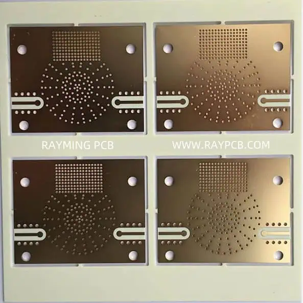
Keep the material data and design model connected
| Reference quantity | Value | How to use it |
|---|---|---|
| Process Dk | 10.20 ± 0.30 | Supplier test reference; do not use its tolerance as a guaranteed Design-Dk tolerance. |
| Design Dk | 11.20 | Starting model value, subject to exact construction and appropriate frequency data. |
| Df at 10 GHz | 0.0022 | Dielectric reference only; not total circuit insertion loss. |
| TCDk | -395 ppm/°C | Typical coefficient; not a life or system-qualification model. |
Process Dk / Df: 10 GHz, 23 °C, IPC TM-650 2.5.5.5; Design Dk: 8–40 GHz differential phase length; TCDk: −50 to 150 °C. Typical source values, not finished-board acceptance limits. In this workbench, Dk and frequency are explicit inputs; no dispersion curve is inferred. Catalogue constructions must be checked for the actual order.
Data checked 17 October 2026 against the Rogers material datasheet. Use the current supplier document when releasing a design.
Choose a layer structure for the RF task
Start with the signal and its reference plane, then add routing, power and mechanical requirements. The workbench records each conductor and dielectric separately. Example layer allocations are discussion starting points, not released manufacturing constructions.
| Architecture | Decision to resolve | Useful next step |
|---|---|---|
| Two copper layers | RF signal on one face, continuous ground on the other. The core is the local dielectric; finish, mask and launches remain separate inputs. | Use the line and thickness comparison tools above. |
| Four copper layers | Define the outer RF cores and central bonding construction; decide whether both faces carry RF. | Review four-layer PCB fabrication and four-layer stackup choices. |
| Six copper layers | Keep RF paths beside continuous grounds while allocating internal power and routing. Specify the FR-4 or RF support core and both bond layers. | Define a six-layer PCB build; use the six-layer stackup guide for layer allocation. |
| Eight or more layers | Resolve additional routing, via transitions, lamination sequence and mechanical balance before freezing dimensions. | Review eight-layer fabrication requirements or discuss a specific construction. |
| RF / FR-4 hybrid or metal-backed build | Specify every bond product, cured thickness, interface and thermal requirement. The online tool does not approve a press cycle or adhesive system. | Use the Rogers multilayer construction guide. |
For other layer counts, follow the multilayer PCB manufacturing route. Material-specific construction and RF acceptance remain part of the RO3010 enquiry.
Thermal sensitivity needs a system limit
A first-order Dk change can shift line phase and impedance even while the dimensions are held fixed. The temperature task exposes that contribution. It excludes physical expansion and complete resonator behavior, so it cannot establish an acceptable passband or operating lifetime.
Do not turn miniaturization into an unconditional claim
Compare the resulting width with the fabrication window and account for conductor thickness, etch shape and transitions. Where the zero-thickness approximation is inadequate, use a validated solver with the released stackup before placing tight dimensions on the drawing.
A starting geometry you can reproduce
For a 50 Ω exposed microstrip using model Dk 11.20, local dielectric height 0.2540 mm and a 10 GHz calculation frequency, this model gives a starting width of 0.2163 mm and effective permittivity 7.3653. A uniform 50 mm path has an unwrapped phase of 1629.48°. These are calculated examples, not measured board results.
Reproduce the values in Line design, then change one input. Before release, replace the example with the agreed construction, include finite copper and mask in an appropriate solver, and confirm how the finished board will be inspected.
Turn design choices into acceptance requirements
| Decision | Include in the RFQ | Resolve before release |
|---|---|---|
| Dk definition | Source, method and selected design value | Was process Dk mistakenly used as the design value? |
| Fine geometry | Line width, etch bounds and copper profile | Is the simple geometry model adequate for the dimensions? |
| Thermal requirement | Temperature range and allowable RF movement | What must the full circuit model and test demonstrate? |
| Manufacturing release | Approved stackup, artwork and inspection scope | Which substitutions require engineering approval? |
Ask for confirmation against the released construction and files. The planning result is a discussion aid; the accepted drawing, quotation and inspection scope define the order.
See the physical features your drawing should define

Mark the relevant gaps, exposed RF conductors, mask boundaries and mechanical interfaces in the released drawing. Agree which dimensions and electrical structures require inspection.
Connect the drawing, the board and its test record
For your RO3010 build, identify the evidence needed before ordering. A useful review connects the same material designation and drawing revision across the stackup, physical inspection and electrical test. The catalogue photograph on this page gives construction context; it does not establish order-specific material identity or RF performance.
1 · Released constructionMaterial, foil, layer sequence, dimensions and revision
2 · Physical constructionRepresentative cross-section, measured dielectric and conductor dimensions
3 · Electrical acceptanceCoupon geometry, test method, reference planes and agreed limits
Illustrative evidence workflow, not a sample inspection report. Request applicable records and agree availability before purchase. RF measurement scope, calibration, fixture correction and environmental testing must be specified; they are not automatically included in a continuity test.
Start the enquiry at your current design stage
| Your stage | Useful starting information | Request |
|---|---|---|
| Selecting a material | Frequency band, mechanical envelope, environment and material candidates. Final artwork is not needed to describe the question. | Check material availability |
| Designing the PCB | Proposed layer sequence, RF reference planes, dielectric / copper dimensions and unresolved requirements. | Request a stackup review |
| Ready for fabrication | Released artwork and drill files, drawing revision, quantity, material specification and acceptance requirements. | Get a quote for this build |
Use the workbench to download a brief if it helps explain the project, or contact the team directly. These links open Contact; they do not upload files or automatically submit tool inputs. Ask the team to confirm the available review scope and quotation requirements.
RO3010 design & procurement questions
Should I design with 10.2 or 11.2?
Use the construction-appropriate design model. The linked datasheet distinguishes process Dk 10.2 from Design Dk 11.2. Do not choose a number merely because it gives a convenient line width.
Does higher Dk guarantee lower cost?
No. Material procurement, usable panel geometry, fine features, processing and acceptance scope all matter. The budget worksheet requires your own cost allowances.
Can the tool qualify a miniaturized RF filter?
No. It supports line-level planning. A filter requires a complete electromagnetic model and verification for its application conditions.
Continue with the decision you need to make
For a different material route, compare the Rogers material families. Use the relevant construction or acceptance guide when the requirement goes beyond this material-specific model.
Model references & limits
The reference line tool uses a zero-thickness approximation; the advanced tool separately identifies finite-copper and grounded-CPW models. Corner results are deterministic bounds from your entered scenarios; no statistical capability is inferred. Measurements and a construction-specific field solver remain the appropriate next steps for release.
- Rogers source datasheet: material values and test conditions.
- Qucs technical reference: microstrip models: Hammerstad–Jensen geometry formulation.
- Qucs: conductor-backed coplanar waveguide: quasi-static mapping and limited finite-copper correction.
- scikit-rf official CPW implementation: implementation convention cross-check; not a measured accuracy claim.