The Role of UL PCB Marking in Printed Circuit Board Safety

High Speed PCB

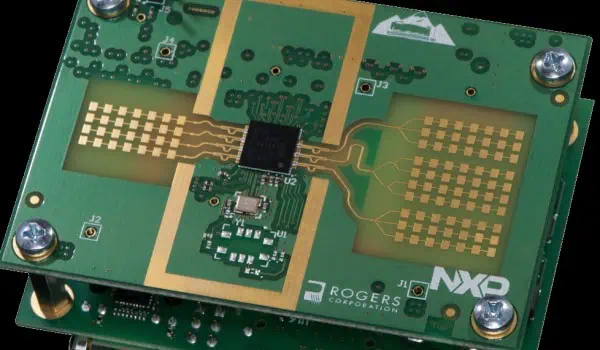
Printed circuit boards are integral components of any electronic device. Therefore, any defect in the assembly process or design can result in product failure. Also, product failure is a huge risk in any electronics manufacturing. Electrical engineers are usually faced with challenges during electronics manufacturing. They are under pressure to build flexible and smaller PCBs to meet the ever increasing demands for modern devices.

This pressure can result in errors during design. Regardless of the go-to-market deadlines and pressure, it is crucial to fabricate a functional board. A circuit board must be functional and safe to use. Therefore, PCB manufacturers must comply with regulatory safety requirements. Also, they must test their products to a high degree of reliability and performance standards.

What is UL Certification for Electronics?

UL is an acronym that stands for Underwriters Laboratories. The core service of this certification is to create safety standards for the electronics industry. These standards are ideal for all types of electronic products such as industrial control equipment and PCBs. The UL identification indicates market acceptance. Therefore, this means that a product has undergone rigorous safety tests.

The UL aims to promote safe working and living environments for humans. Also, UL can achieve this by applying hazard-based safety engineering. The UL mark supports the manufacturing and use of products that are environmentally and physically safe. Also, UL certifies, validates, and tests materials used for electronics production.

The concern for end product safety is what drives the UL recognition of components. The UL marking is usually required when safety becomes a critical issue.  This marking is a widely accepted proof that indicates the safety of a product. Also, the UL marking meets the Canadian and American safety standards.

UL is a third-party certification company established in Chicago in the year 1894. This certification company verifies the safety of a product to make the world a safer place. Also, UL creates industry standards when innovating new products. This safety organization checks these products regularly to help ensure they still meet up with the UL standards.

UL certification reveals the quality and safety of a PCB product. Also, UL recognized boards are globally accepted. With UL 94, board manufacturers can assure customers that their products meet specific requirements. Manufacturers fabricate rigid flex PCBs to meet UL standards.

What is UL Marking on PCB?

In addition, this marking is a symbol of product safety for consumers. Therefore, all PCBs must have the UL marking. This marking can be a great marketing tool for businesses. Also, this is a major reason why most manufacturers strive to get the UL marking on their products. However, a product doesnโ€™t just get the UL marking except it passes some safety tests.

A UL marking on a PCB indicates that a circuit board meets all safety and flammability requirements. Also, a UL mark indicates that your circuit board meets the UL requirements. The UL 94 is an important standard for assessing the quality of a board. Therefore, UL 94 covers all flammability requirements for PCBs.

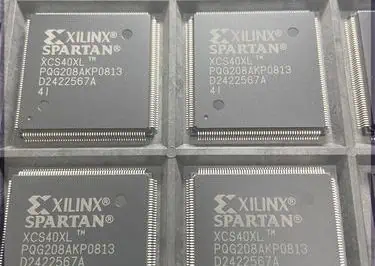
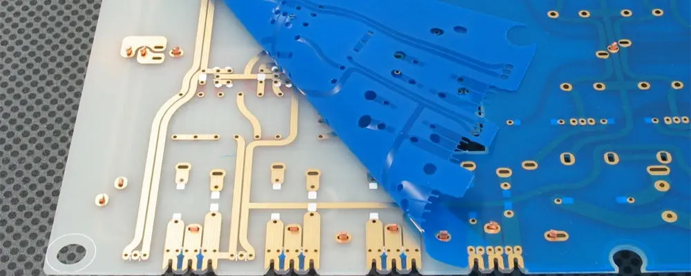
The PCB material must meet the specified flammability level of UL 94. Also, UL 94 V0 is a PCB certification for FR4 materials. This indicates that a PCB material will self-extinguish within 10 seconds. FR4 PCB are UL certified PCBs. All PCBs with UL 94 certification must undergo flammability testing. Also, flammability testing helps to ensure fire protection and electrical safety.

As long as fire protection and electrical safety are crucial, the UL 94 certification is necessary. Also, a board with UL certification is safe for use in electronic devices. Flexible dielectric film materials also require UL certification.

What is UL Classification?

There are two main classes of UL certification in electronic products. These are the UL recognized component mark and the UL listed label.

What does UL recognized mean?

UL recognized doesnโ€™t apply a seal of approval to end products. Also, the UL recognition service focuses on parts and machinery that manufacture the products. This means that it certifies a component in a larger mechanism. Most times, factories get UL recognition. UL recognition checks the efficiency and safety of machinery used during production. Also, it encourages companies to go for more sustainable practices.

The UL standards ensure that all pieces of equipment are properly housed. However, this may require installation precautions. It is much easier to get UL recognized stamps than UL listed. This is because it is easy for manufacturers to select which components are certified within a bigger system.

What is a UL Listing Mark?

UL Listed is usually featured on a wide swath of consumer electronics today. The type of product UL Listed certifies differentiates it from UL recognized. While UL recognized is for components, UL listed is meant for stand-alone products. Although, they both ensure safety, they are widely used in different capacities and different products.

 UL listed is more recognizable than UL recognized. This is because it ascertains the safety of consumer products. UL listed certification requires more testing. Also, the UL listed seal indicates that the UL has tested a product to recognized safety standards. Furthermore, UL listed products are free from a foreseeable risk of electric shock and fire in a Division 2 environment.

Therefore, the UL listed marking ascertains the longevity and safety of several household electronics subjected to rigorous use everyday. The UL listed approval benefits both the manufacturer and consumer.

Why is the UL Marking Important in PCBs?

The UL recognition and certification is a strong marketing tool for business. Also, UL ensures manufacturers test their products by following established procedures to reduce safety problems. Products certified by UL always undergo stricter performance tests.  PCB materials and components recognized by UL must have undergone the most stringent safety testing. There are many reasons why the UL marking is important in the PCB manufacturing process.

Great reputation

UL has built a great reputation. This certification company instills a sense of trust in consumers. Also, UL certification has a long standing reputation in the PCB industry.

Safety and quality

This certification company ensures products meet the highest safety requirements.  Being UL certified indicates a manufacturerโ€™s dedication to the safety of consumers. Asides assuring safety, this certification also assesses the quality of a PCB. Also, the UL safety standards improve the quality of PCBs. UL certified PCBs are safe and reliable.

Customer Security

Consumers are always assured of a productโ€™s safety when it has the UL stamp of approval. For instance, the UL certification may be a factor to consider when purchasing a circuit breaker. UL focuses majorly on guaranteeing the safety of a product.  A consumer will prefer to opt for a product that has the UL logo.

Improved functionality

UL certification enables a PCB company to innovate its standards for safety. Also, it enables PCB manufacturers to integrate the best practices in the industry. Therefore, this results in improvement in the functionality and performance of PCBs. UL marking helps PCB manufacturer to offer PCB assembly services across the world.

Classifications of UL94

The UL94 is a standard for the flammability safety of parts used in devices. The underwriters laboratory of the US established this plastics flammability standard. This standard determines the tendency of a material to spread flame or extinguish once you ignite it. Below are the classifications of UL94

V- 0

In this classification, the burning stops within 10 seconds on a specimen. This classification allows drips of particles if they arenโ€™t inflamed.

V-1

Here, burning halts just within 30 seconds on a vertical specimen. It allows drips of particles if they arenโ€™t inflamed.

V-2

In this UL 94 classification, burning halts within 30 seconds when it is on a vertical specimen. Also, it allows drip of flaming particles.

5VA

Here, burning halts within 1 minute on a vertical specimen. 5VA doesnโ€™t allow drips of particles. Also, plaque specimens may not have a hole.

5VB

Also, burning stops within 1 minute on a vertical specimen. No drips are also allowed.

HB

Also known as horizontal burning, it is the least flame retardant. There is slow burning on a horizontal specimen.

What to Consider When Specifying a PCB that Needs UL Recognition

 It is crucial to specify the right PCB when requesting UL recognition. The intended application of the PCB will determine the parameters needed for your circuit board. A PCB may require a flame rating only. Sometimes, a PCB may need MOT, a minimum CTI value and flame rating.  Below are UI parameters to consider:

Specific flame rating

The end-product requirements help to specify the least acceptable flame class. Also, classification represents burn time and small sample evaluation. V-0, V-1, and HB are examples of flame classes.

Maximum operating temperature (MOT)

This represents the maximum continuous use temperature of a circuit board. Also, the requirements of the end-product help to specify maximum temperature.

Minimum CTI rating

Comparative tracking index (CTI) is usually evaluated on laminate materials. Also, these values are a performance level category.

Direct support (DSR) compliance

DSR refers to the performance characteristics for recognized PCB materials in contact with current carrying parts at 120V or lower. The available PCB materials determine the PCB DSR compliance. You can manufacture a PCB type using DSR compliant materials. In such a case, there will be a DSR triangle on the listing card.

Multiple soldering processes

Most manufacturers use SMT. Manufacturers subject some boards to multiple reflow cycles. Multiple solder limits represent the temperature profile while soldering. Specify a PCB with multiple solder limits.

Conclusion

UL marking indicates the performance and safety of a machinery or end product. This marking is an easy way to make your products and business highly rated. Flammability and electrical safety are crucial UL parameters. These UL parameters are critical issues in PCB manufacturing. Printed circuit boards that meet UL requirements are safe for use.

What are Top 10 largest Electronics Parts Suppliers in China?

Electronics Parts Supplier

China has firmly established itself as the electronics manufacturing hub of the world. Much of this phenomenal growth has been fueled by the rise of major Chinese electronics component suppliers catering to local and international customers. This article profiles the 10 largest electronics parts suppliers in China based on their revenue, product portfolio, capabilities, reputation and global reach.

1. Foxconn

Foxconn is the worldโ€™s largest electronics contract manufacturer and a major supplier of components and assemblies. Some facts about Foxconn:

  • 2021 revenue – $175 billion
  • Flagship products – connectors, enclosures, cables, PCBs
  • Headquarter – Taiwan
  • Facilities – China, India, Europe, Americas
  • Customers – Apple, HP, Dell, Xiaomi, Sony

With expertise spanning components, modules and complete devices, Foxconn provides end-to-end manufacturing capabilities at massive scale. Its Connectivity Product Business Group offers connectors and other components.

2. Luxshare Precision

electronic parts manufacturer

Focused on interconnect and mechanical solutions, Luxshare has grown rapidly as a preferred supplier to Apple and other giants:

  • 2021 revenue – $15.1 billion
  • Products – connectors, cables, acoustics, modules
  • Headquarters – Dongguan, China
  • Facilities – 15 plants across China
  • Key customers – Apple, Huawei, Oppo, Xiaomi, Bosch

Luxshare possesses advanced capabilities in high-speed interconnects and precision plastics. It has leveraged strategic customer relationships into diversified business lines.

3. AAC Technologies

AAC Technologies produces components for smart devices and electrified vehicles:

  • 2021 revenue – $3.1 billion
  • Products – MEMS microphones, speakers, haptics, optics
  • Headquarters – Shenzhen, China
  • Facilities – Mainland China, Vietnam, Singapore
  • Customers – Apple, Huawei, Xiaomi, OPPO, vivo

AACโ€™s miniaturized acoustic, optical and haptic components enable smart device innovations. It is accelerating growth in emerging segments like electric vehicles.

4. Sunwoda Electronic

Sunwoda provides advanced passive components and boards for high-end products:

  • 2021 revenue – $2.2 billion
  • Products – capacitors, inductors, resistors, specialty PCBs
  • Headquarters – Harbin, China
  • Facilities – China, Vietnam
  • Customers – Apple, Huawei, OPPO, vivo, Xiaomi

Leveraging precision manufacturing techniques, Sunwoda caters to quality-focused customers with custom components rated for high reliability.

5. Rayming Technology

Rayming specializes in high-performance interconnect solutions:

  • 2021 revenue – $1.8 billion
  • Products – connectors, antennas, flexible/rigid-flex PCBs
  • Headquarters – Suzhou, China
  • Facilities – Suzhou, Chengdu
  • Customers – Apple, Huawei, General Motors, Boeing, Siemens

Raymingโ€™s expertise in precision interconnects, specialty PCBs and miniaturized RF devices supports innovation in consumer tech and industrial applications.

6. Primax Electronics

Primax makes input devices, speakers and other components:

  • 2021 revenue – $1.3 billion
  • Products – keyboards, mice, headphones, buzzers, power banks
  • Headquarters – Taipei, Taiwan
  • Facilities – China, Taiwan, Thailand, Myanmar
  • Customers – Dell, Logitech, Razer

By integrating design, acoustics and optics expertise, Primax delivers high value human interface devices and audio solutions.

7. LCE Technology

Specializing in advanced passives, LCE products enable cutting-edge electronics:

  • 2021 revenue – $830 million
  • Products – MLCCs, tantalum capacitors, chip resistors
  • Headquarters – Wuxi, China
  • Facilities – China
  • Customers – Xiaomi, OPPO, vivo, nubia, Meizu

LCEโ€™s portfolio ranging from consumer to automotive applications provides components optimized for emerging requirements like 5G, EV and IoT systems.

8. Goertek

Goertek is a leading manufacturer of smart acoustic components:

  • 2021 revenue – $790 million
  • Products – microphones, speakers, acoustic modules
  • Headquarters – Weifang, China
  • Facilities – China, Vietnam, Mexico
  • Customers – Apple, Samsung, Xiaomi, Huawei, Oppo, Dell

Leveraging vertical integration from components to finished modules, Goertek enables sophisticated audio and voice capabilities in end-user devices.

9. Shenzhen Deren Electronics

Deren crafts specialty interconnect solutions for high-speed applications:

  • 2021 revenue – $590 million
  • Products – high-speed connectors, flexible/rigid PCBs
  • Headquarters – Shenzhen, China
  • Facilities – Shenzhen and Huizhou, China
  • Customers – Huawei, ZTE, Samsung, vivo, OPPO, Xiaomi

With expertise in high frequency design, Deren caters to communication infrastructure markets with advanced components rated for 100Gbps and beyond.

10. Dongguan Meadville Electronics

components manufacturers

Specializing in embedded electronics modules, Meadville enabling local OEM capabilities:

  • 2021 revenue – $500 million
  • Products – PCB assemblies, display modules, electromagnetic components
  • Headquarters – Dongguan, China
  • Facilities – Dongguan and Guangzhou, China
  • Customers – Xiaomi, vivo, OPPO, Lenovo, Hisense, Gree

By providing value-added assemblies and modules, Meadville aids domestic brands in quickly implementing cutting-edge electronics systems.

Comparing Business Models of Major Suppliers

While deeply invested in electronics manufacturing, major Chinese suppliers employ varied strategic approaches:

CompanyBusiness Model
FoxconnContract manufacturing for global OEMsย ย – Integrated components to complete products
Luxshare– Strategic supplier for Apple and Chinese brandsย – Interconnect focus from ICs to cables
AAC– Acoustic components for smart devicesย ย – Direct to device brands
Sunwoda– Advanced passive componentsย ย – High-mix low-volume for quality focus
Rayming– Miniaturized high-speed interconnectsย – Flex-rigid PCB innovation
Primax– Human interface devicesย ย – Combined design, acoustics and optics
LCE– State-of-the-art passive componentsย ย – Supporting domestic brands
Goertek– Acoustic and haptic solutionsย ย – Custom modules development
Deren– High-frequency interconnectsย ย – Communication infrastructure
Meadville– Value-added modules and assembliesย ย – Enabling local OEMs

This diversity of strategies sustains a rich electronics ecosystem.

Driving Factors for Growth and Success

Chinaโ€™s electronics supply chain has thrived due to key factors:

Government Support – Policy, incentives and infrastructure catalyzing electronics manufacturing growth.

Technology Transfer – Absorbing expertise from foreign partnerships and acquisitions.

Local Market – Enormous domestic demand enabling scale and steady revenues.

Specialization – Developing expertise in specific technologies through concentration.

Ecosystem – Comprehensive supply chain ensuring accessibility of materials, equipment, labor and logistics.

Cost Efficiency – Highly optimized operations and manufacturing excellence.

Quality Improvements – Investments in better process control, automation and quality culture.

IP Development – Increasing R&D investments to create proprietary technologies and IPs.

These factors will likely continue propelling the growth of Chinese electronics suppliers on the global stage.

Future Prospects

Major trends impacting the future of top Chinese electronics suppliers:

  • Global Expansion – Leveraging existing customer relationships and cost advantages to grow internationally.
  • High-End Markets – Moving beyond commoditized products into value-added components for premium applications.
  • Vertical Integration – Expanding scope across the supply chain for greater consolidation and revenues.
  • Technology Leadership – Accelerating R&D and IP development for next-generation products.
  • Sustainability – Adopting greener technologies, renewable energy and circular economy practices.
  • Automation – Embracing Industry 4.0 transformations for smart manufacturing.
  • Co-development – More strategic partnerships with customers for technology co-development.
  • Mergers & Acquisitions – Targeted M&A for gaining expertise, IP and access to new markets.

With these moves, Chinese suppliers are maturing into advanced innovation partners capable of catering to the most demanding industries globally.

Conclusion

circuit board electronic components

Driven by tremendous domestic demand and supportive government policies, Chinese electronics component suppliers have rapidly grown in scale, technology sophistication and global competitiveness. Companies like Foxconn, Luxshare and AAC are now established leaders in their respective product segments. A rich ecosystem of specialized suppliers produces components critical for cutting-edge devices and infrastructure. With further expansion internationally, investments in modern manufacturing and deeper technology partnerships, Chinaโ€™s electronics supply chain will become indispensable for customers worldwide needing high-quality, cost-optimized and leading-edge solutions.

Frequently Asked Questions

Which Chinese electronics suppliers lead in component miniaturization?

AAC Technologies and Goertek stand out in acoustic component miniaturization to fit smart devices. Luxshare offers ultra miniature connectors. Rayming technologies provides tiny antennas and flexible PCBs. LCE produces smallest passive devices through advancements like MLCCs.

Do the large suppliers only focus on high volumes?

Larger players indeed cater to high-volume customers for economies of scale. However, companies like Sunwoda and Deren still focus on lower volume, high-mix specialty components where China is increasing expertise through better process control.

Which segments are growing fastest for these suppliers?

Automotive electronics is witnessing rapid growth as suppliers adapt solutions for ADAS, electrification, connectivity in vehicles. High-speed communications is another fast-growing segment with 5G and data center expansions.

Does China lack innovation compared to other electronics hubs?

The perception of lacking innovation is fading quickly as Chinese companies ramp up R&D investments and IP development. Luxshare, Goertek and others are now globally recognized for advanced proprietary technologies. But there is still scope to enhance fundamental research.

How should global OEMs manage relationships with these suppliers?

Strategic partnerships via technology sharing and co-development are ideal rather than pure supplier-buyer relationships. This allows leveraging the enormous manufacturing capacities in tandem with improving capabilities. Quality expectations must be clearly defined and enforced.

What are the Capabilities and Processes Involved in Custom PCB Assembly?

PCB prototype assembly suppliers

One very challenging aspect when it comes to the process of electronic manufacturing is PCB assembly. You have to do it properly whether in medical equipment, digital watches, Smartphones, or industrial machines.

The best part of this is that this article covers everything you need regarding the PCB assembly process. We will be focusing on what PCB assembly is, the applications, assembly process, and more. Please letโ€™s begin by explaining what PCB assembly is.

What is PCB Assembly?

Have you discovered that boards usually have several components which are attached firmly? What are they?

The truth is that so many think theyโ€™re just for decoration. This isnโ€™t true! In the absence of these components, the PCB cannot function independently. This means that each of these components is significant and vital to the boardโ€™s functioning.

Speaking technically, when you detach any of the components, the operation or functioning of the printed circuit board or advanced circuits is impaired. The embedding of these elements is seen via a unique manufacturing process. Therefore, this is a process we call PCB Assembly Process.

Any printed circuit board that has passed through this entire process is an assembled printed circuit board. Looking closely at the circuit board, some copper lines become visible. This is what we call traces. Although they are tiny, they serve a very important purpose.

The traces help in linking the connectors and all the components of the printed circuit boards electrically amongst themselves. Printed circuit boards serve both simple and complex functions.

In contrast to other devices, size isnโ€™t important here. The fact is that some are thin and tiny, yet they keep functioning in an optimal way and run different complicated tasks.

What are the Processes Involved in PCB Assembly?

There are several processes involved in Prototype PCB assembly. Let us consider them.

There are three main assembly processes here:

Surface Mount

In contrast to the through hole technology, the process of SMT is distinct when it comes to manufacturing efficiency. Surface mount technology features the whole automatic process of mounting. This begins from the printing of the solder paste, then to the pick & place, and lastly to the reflow soldering. Letโ€™s quickly consider the important steps here.

Solder Paste Printing

This involves the application of the solder paste on a circuit board using the solder paste printer. In order to ensure that the solder printing is accurate where you are mounting the components, a template can be useful. The sheet is the solder screen or the stencil.

Due to the fact that the majority of manufacturers deal with products of high-quality, thereโ€™s a need to inspect these products immediately after the solder paste printing.

Mounting of the Components

Once you are through with the printing of the solder paste, then the PCB is automatically sent into the pick and place machines.

In this case, with the solder paste, the components as well as the integrated circuits are mounted on the pads. The components will be installed expertly on the circuit board making use of the machineโ€™s component reels. For this process, component reels serve a very important process.

Their rotation helps in supplying parts to machines which attach pieces subsequently to circuit boards.

Reflow Soldering

After the parts are all mounted on the board, the next step is passing the PCB to the furnace. This should have a temperature of about 223 degrees. This high heat allows the easy melting and liquefying of the solder paste.

 After the application of severe heat, the board is allowed to cool down. This makes the solder solidify firmly, thereby binding the components of the SMD onto the board.

Through Hole

For the thru hole, holes are inserted into the PCBs. After this pin through hole components are then inserted. You can achieve all these through soldering. Thru hole involves these steps.

Placing the components

Make sure you check the design documents of the circuit board. Working with this, arrange and also fix the components.

Check and rectify

This second step involves the plugging of the components and boards together. If you encounter any issue using the method of soldering; thatโ€™s if there’s any inconvenience or disturbance.

Soldering

This step, wave soldering can only be achieved at high temperatures. This is the only way that you can overcome the issue. You can achieve this through circuit board movement in liquid solder through waving.

Mixed Technology

For this, both surface mount and through-hole technologies are used in solving complexity. They are used for the following situations.

Single sides mixed

These procedures such as printing making use of solder paste, placing the parts of the surface mount devices, then reflow soldering, placing through thru-hole technology, as well as wave soldering, respectively are very important to achieve.

Double sides mixed

For this, the process of PCB assembly can be achieved in both ways either without adhesive or with adhesive. The adhesive step of the SMT is optional.

You will use the entire steps for the single side as well as use among the two sides. For non-adhesive, thereโ€™s no need to follow the SMT adhesive step.

PCB Assembly Capabilities

One measure that PCB assembly must accommodate is lead-free construction and production of electronics, as well as RoHS compliance. In this section, we will be considering the well-known PCB assembly capabilities.

Flex PCB Assembly

Suitable assemblies should be able to design different PCBs. One of these is the flex PCB. Flex PCBs are well-known because they can be bent through many angles. They also eliminate errors in pcb manufacturing and they can assume different designs and shapes.

PCB Stencil

Let me remind you of what a PCB stencil is. During soldering, there is a printer for the solder paste, whereby the board is covered by a clear template. The template ensures that this solder paste remains accurately on the right locations where integrated circuits and components should be mounted.

The template is called PCB Stencil. You can also call it solder screen.

Prototype PCB Assembly

Reliable PCB manufacturers ought to be able to offer budget-friendly and quick prototype assembly. Providing these services offers the following benefits:

  • The designsโ€™ maintenance is confidential
  • Freedom to experiment and create quickly and at lower costs
  • Lowers the R & D time, which leads to quick time to the market
  • Provides chances of adjusting, reworking, tuning, and trimming the PCBs

Component Sourcing

Component sourcing has brought lots of benefits, which includes line efficiency. In addition, it allows more time for project engineering, designing, and PCB manufacturing.

Components sourcing involves procuring the parts from a well known certified electronic components distributor. It also deals with acquiring parts from endorsed dealers and channels.

Turnkey PCB Assembly

This assembly process means that the dealer will handle everything regarding PCB solution, picking, components procurement, placing of components, and manufacturing.

What are PCB Assembly Services?

Now, with all the knowledge you have acquired on PCB assembly, the next question that will probably be on your mind should be where can I order PCB assembly service?

The good news is that we will be answering this question regarding PCB assembly service right in this section. This is a sensitive issue that must not go wrong. Sure you want a company that offers pcb assembly services that meets your demands and specifications, most especially board quality. This should be the major objective of companies offering PCB assembly services.

Below are some steps you consider

Work with a good and reasonable timeframe

Make sure you comprehend what this company will deliver before you go ahead to sign a non disclosure agreement with them. Know the minimum order, lead time, and the entire time needed for the pcb prototype assembly.

Consider the experience of the Company in offering PCB assembly services

Note that exposure and experience in PCB assembly is very important. You can check the companyโ€™s website for the following.

  • Batch sizes preferred buy the company
  • How long this company has been functioning
  • Firms they have partnered with previously
  • Products they have manufactured
  • How long they have been involved in THT or SMT or both

Access the Quality

Choose a company that offers high-quality jobs. You can order something small to see if their quality matches what you expect.

Is there Customer Support?

Another aspect is having customer support. Does this company offering PCB assembly have good customer support? Are they available to assist customers with PCB assembly or to fix any technical issue? Will they be flexible enough to work with your timeline?

Compare the costs

You should get great value for any money you spend and also it has to be at an affordable price. Finance is important and so also quality is very important. Therefore, make sure you compare the costs and also ensure the quality before making any move.

Warning Signs

Beware of this warning signs and

  • Longer time for project completion
  • Exaggerated pricing
  • Inflexibility or rigidity of this company to seek answers to problems relating to your work
  • Poor communication and unresponsiveness

Conclusion

Here comes the end of the article on printed circuit board assembly. You now have what it takes to be involved in PCB assembly. Make sure you refer to this guide at all times. If you need a reliable company for your PCB assembly, contact us at Rayming PCB & Assembly and get an instant quote.

Types, Properties, and Advantages of Al2o3 PCB

Al2o3 PCB

The manufacturing of a circuit board involves the use of several materials. Aluminum is a common material found in ceramic PCB. It is not only common, it is the most-effective material used in ceramic PCB. The two most common ceramic materials used for a ceramic PCB are aluminum oxide (Al2o3) and aluminum nitride (AIN).

Al2o3 features much higher thermal conductivity than AIN. However, a ceramic printed circuit board is a great option for several applications. Our focus here is on Al2o3 ceramic PCB. Therefore, this article will shed more light on the properties and importance of Al2o3 PCB.

What is Al2o3 PCB?

Al2o3 PCB or Alumina PCB is a circuit board that comprises Al2o3. It is a type of ceramic PCB features good properties which include low CTE and good thermal conductivity. Also, Alumina comprises many isomorphic crystals and higher purity. The most crucial property of this ceramic PCB is its thermal conductivity which is between 15W/mK to 50W/mK.

This ceramic PCB is ideal for use in a wide range of applications. Some of its application areas include LED boards and high frequency devices. Al2o3 PCB features ceramic material for multilayer packages. This PCB has undergone several layers of experiment. Also, it has developed over the years.

Al2o3 is an engineering material that provides great electrical and mechanical properties.  Alumina is the most used ceramic material. Also, Alumina PCBs comprise a great amount of Al2o3. The high thermal stability of alumina boards helps to enhance the thermal efficiency and performance of the circuits used in automobiles.

Alumina PCBs can feature 95.5%, 75%, and 96% alumina substrates. Higher purity indicates denser appearance and smoother surface. These circuit boards offer excellent electrical insulation. Also, alumina as a ceramic material features high biocompatibility. The material properties of alumina PCB contribute to its performance.

Types of Alumina PCB

Al2o3 PCB comprises three types of alumina oxide. This includes 99.5% alumina substrate, 99.6% alumina substrate, and 96% alumina substrate.

99.5% Alumina ceramic substrate

This alumina PCB is widely used in smaller grain size applications. Also, the finish on the surface of this PCB is 99.5% and can achieve a 2u-in maximum finish. This is because it is a large grain size. Also, the materials have less thermal conductivity and flexural strength. One of the benefits of this substrate is that it is available in other thickness and larger sizes.

99.6% alumina PCB substrate

This substrate is widely known for its standardized thin-film substrates. Therefore, this contributes to its popularity in the PCB industry. 99.6% alumina substrate is ideal for use in evaporated and sputtered metals. Also, this substrate features a high purity level. There is a smaller grain that allows it to offer a smoother result without fewer surface defects.

Also, this substrate has below 1u-in 99.6 Alumina surface roughness. Therefore, this indicates low thermal conductivity, good dielectric properties, and great electrical insulation.

96% alumina PCB substrate

This alumina substrate is very common. Also, the majority of microelectronic applications require alumina PCBs. The standard format needed for this type of application is the thick film substrate. The 96% alumina PCB substrate is used for designing hybrid microelectronic circuits.

96% alumina substrate is effective for building hybrid devices. This is because of its high technical quality and availability. Also, it provides good thermal conductivity and low coefficient of thermal expansion.

Al2o3 PCB Manufacturing

Alumina is an important material used for fabricating printed circuit boards. Also, alumina PCB materials feature unambiguously diverse properties. This ceramic PCB is specially made of ceramic components. Also, the properties of alumina are different from other metals. Therefore, this establishes a major difference in the fabrication of Al2o3 PCB than the others.

Alumina PCB has some purposes it serves in the PCB industry. Where other PCBs arenโ€™t applicable, Alumina is the perfect option to choose. The rigid and strong material used in Alumina PCBs offer significant support to electronic components.

Al2o3 is a perfect substitute to include for mounting on the PCB surface. The performance is great enough when compared to other materials. Also, there is higher temperature consistency compared to other materials. The only limitation of these materials is that it can be more expensive than other usual materials. However, this occurs when you use it for some high-grade devices.

Alumina PCB requires no dielectric layer between the core and the circuit. Also, PCBs that comprise alumina are usually thicker. Alumina PCB requires complicated procedures at high temperatures irrespective of the manufacturing process adopted.

The manufacturing process of a ceramic PCB involves several steps. The direct bonding copper is essential during manufacturing. Ceramic printed circuit boards offer strong thermal dielectric. This metal base PCB features the thick film printing and thick film process. The surface finish used for alumina ceramic PCB matters. Immersion gold is a good example of surface finish for aluminum oxide PCB.

Direct plated copper technologies are widely used in the manufacturing process. Also, direct plating copper impacts the performance of a board.

Properties of Al2o3 PCB

Alumina oxide is a common material used in fabricating ceramic PCBs and packages. Also, alumina boards offer great mechanical and electrical properties which make them highly preferred for fabricating circuit boards. The absolute material properties of this PCB includes:

Low thermal conductivity

The thermal conductivity of this PCB ranges from 15W/mK to 50W/mK. When the IC or LED produces high heat, the heat directly and quickly transfers to the alumina PCB. Therefore, there is no need for an insulating layer when using an alumina board.

High melting point

The melting point of a 96% alumina substrate is 1400oC. 99% alumina substrates have melting point of  1600oC.

Great hardness and electrical insulation

Alumina PCBs feature excellent electrical insulation. Due to this property, this circuit board is widely used in high-performance applications. The reflectivity test reference thickness helps in determining the thickness of this PCB.

Lower coefficient of thermal expansion

The coefficient of thermal expansion of this ceramic PCB matches components. Also, the CTE ranges from 6 ppm/oC to 8 ppm/oC.  Therefore, the lower coefficient of thermal expansion results in less stress on solder joints.

Advantages of Alumina PCBs

Ceramic PCBs offer a lot of advantages. Below are the most upgrading benefits of Al2o3 PCBs:

  • It comprises rigid and strong material that boosts durability
  • Ensures ideal mechanical strength in the ceramic PCBs
  • It restricts outgassing
  • Features great compressive strength
  • This ceramic PCB offers excellent gliding properties and low density
  • Also, it provides enough light reflection as a result of its white material
  • It features high operating temperature which ranges from 350iC to 1500iC
  • The package size is small due to the possibilities and integration in multilayer applications
  • Also, the hermetic packages allow 0% water absorption
  • This ceramic PCB contributes to unmatched wears and corrosion resistance
  • Also, it offers more excellent performance in high-frequency applications
  • It is relatively low cost

Conclusion

Ceramic substrates are commercially available material. These substrates offer great electrical and thermal properties. The lower expansion coefficient and high temperature resistance are examples of these properties. Al203 PCB is ideal for different applications. We at RayMing provide quality Al2o3 PCB at competitive pricing.

Why High-Speed PCBs Demand Low-Dk/Df Materials ?

High-Speed High-Density PCB

In today’s electronics landscape, the relentless push for faster data transfer and processing speeds has transformed how engineers approach printed circuit board (PCB) design. High-speed PCBs have become the backbone of modern electronics, enabling everything from lightning-fast internet connections to advanced driver assistance systems in vehicles. Yet, as frequencies climb and signal rise times shrink to picoseconds, the very materials used to construct these boards have become critically important.

This article explores why low dielectric constant (Dk) and low dissipation factor (Df) materials are not merely beneficial but essential for high-speed PCB performance. Whether you’re designing next-generation telecommunications equipment or wrestling with signal integrity issues in your current project, understanding these material properties could be the difference between a mediocre and exceptional product.

What Is a High-Speed PCB?

Rogers-RO4360-pcb

Before diving into material considerations, let’s clarify what constitutes a “high-speed PCB.” Unlike conventional circuit boards, high-speed PCBs are specifically designed to maintain signal integrity at elevated frequencies and data rates.

Defining High-Speed in Modern Electronics

High-speed PCBs typically involve one or more of these characteristics:

  • Signal rise times below 1 nanosecond
  • Operating frequencies above 1 GHz
  • Data rates exceeding 1 Gbps
  • Transmission line effects becoming significant

It’s worth noting that “high-speed” is a relative term that continues to evolve. What was considered blazingly fast a decade ago might be regarded as moderate speed today. The threshold keeps advancing as technology progresses.

Real-World Applications

High-speed PCBs are ubiquitous in modern electronic systems:

  • Network infrastructure (routers, switches, servers)
  • High-performance computing platforms
  • 5G telecommunications equipment
  • Automotive radar and ADAS systems
  • High-definition video processing
  • Memory interfaces (DDR4/5, GDDR6)
  • High-speed storage systems (NVMe, PCIe 4.0/5.0)

Signal Speed vs. Clock Speed

One common misconception is equating a PCB’s “speed” with its clock frequency. While clock frequency is important, signal integrity depends more on signal rise timeโ€”how quickly a signal transitions from low to high. Faster rise times mean higher frequency components in the signal, requiring more careful attention to the board’s material properties.

As rise times decrease below 1 nanosecond, transmission line effects become pronounced, and the PCB substrate material significantly impacts signal propagation. This is where dielectric properties become crucial.

Read more about:

Understanding Dielectric Constant (Dk) and Dissipation Factor (Df)

The performance of high-speed PCBs hinges on two key material properties: dielectric constant (Dk) and dissipation factor (Df). Let’s break down what these properties mean and why they matter.

What is Dielectric Constant (Dk)?

The dielectric constant, often denoted as Dk, ฮตr, or simply “Er,” measures how much a material concentrates electric flux compared to a vacuum. In simpler terms, it indicates how much a material slows down electrical signals passing through it.

A vacuum has a Dk of exactly 1.0, while PCB substrate materials typically range from 2.2 to 4.5. Lower Dk values mean signals travel faster through the material, which is generally desirable for high-speed applications.

The dielectric constant directly affects:

  • Signal propagation velocity
  • Impedance characteristics
  • Electrical wavelength in the material

What is Dissipation Factor (Df)?

The dissipation factor (Df), also known as the loss tangent or tan ฮด, measures how much signal energy is lost as heat within the dielectric material. It represents the inefficiency of the dielectric material.

A lower Df value indicates less signal loss, which means:

  • Reduced signal attenuation
  • Better signal integrity over distance
  • Less power lost as heat
  • Improved high-frequency performance

Typical Dk/Df Ranges for PCB Materials

PCB substrates exhibit a wide range of dielectric properties:

Material TypeTypical Dk RangeTypical Df Range
Standard FR-44.0-4.70.017-0.025
Mid-performance3.5-4.00.008-0.015
High-performance2.8-3.50.002-0.007
Ultra-low loss2.2-2.80.0009-0.002

Each material category serves different application needs, with higher performance materials generally commanding higher prices.

Why Low-Dk/Df Materials Are Essential for High-Speed PCBs

As frequencies climb above 1 GHz and data rates exceed multi-gigabit speeds, the material composition of PCBs becomes increasingly critical. Let’s explore why low-Dk/Df materials are not just beneficial but essential for high-speed PCB performance.

Signal Integrity Benefits

Minimizing Signal Delay

Lower Dk materials allow signals to propagate faster through the PCB. This becomes crucial in high-speed designs where timing margins are tight, and signal delays must be carefully managed.

The propagation delay (tpd) in a PCB trace is directly proportional to the square root of the dielectric constant:

tpd โˆ โˆšDk

For time-critical applications like DDR memory interfaces, where timing skew must be minimized, low-Dk materials provide essential performance advantages.

Reducing Signal Reflections

When signals encounter impedance discontinuities, reflections occur. These reflections can cause signal integrity issues like ringing and overshoot. Low-Dk materials enable more precise impedance control, reducing the likelihood of impedance mismatches and associated reflections.

Minimizing Signal Loss

Insertion Loss Reduction

Signal attenuation becomes a major concern at high frequencies. The dissipation factor (Df) directly contributes to insertion loss, which increases with frequency. Lower Df materials significantly reduce this loss, allowing signals to maintain integrity over longer distances.

The relationship between insertion loss and Df is approximately:

Insertion Loss (dB) โˆ Frequency ร— Df

This means that as frequencies increase, the benefits of low-Df materials become exponentially more important.

Maintaining Signal Shape

High-frequency signals are particularly vulnerable to dispersionโ€”different frequency components traveling at different speeds. This can distort the signal shape, causing issues like intersymbol interference in digital systems. Low-Dk/Df materials help maintain signal fidelity by reducing dispersion effects.

Improved Design Flexibility

Enhanced Routing Capabilities

Low-Dk/Df materials allow for:

  • Longer trace lengths before signal degradation becomes problematic
  • Tighter routing constraints while maintaining signal integrity
  • Reduced need for signal conditioning components
  • More reliable performance across manufacturing variations

Frequency Consistency

Premium low-Dk/Df materials typically exhibit more stable dielectric properties across frequency ranges. This consistency is valuable for broadband applications where performance must be maintained across multiple frequency bands.

Comparing Common PCB Materials for High-Speed Applications

The PCB industry offers a spectrum of materials with varying performance characteristics. Let’s compare the most common options for high-speed applications.

FR-4 vs. High-Performance Laminates

Standard FR-4

For decades, FR-4 has been the workhorse of the PCB industry. This glass-reinforced epoxy laminate offers:

  • Dk: 4.0-4.7
  • Df: 0.017-0.025
  • Good mechanical stability
  • Excellent cost-effectiveness
  • Widespread manufacturing support

However, standard FR-4 becomes problematic above 1-2 GHz due to its relatively high Df and Dk variation with frequency.

High-Performance FR-4

Modified FR-4 materials with enhanced dielectric properties bridge the gap between standard FR-4 and premium laminates:

  • Dk: 3.5-4.0
  • Df: 0.008-0.015
  • Moderate cost increase
  • Suitable for applications up to 5-10 GHz

Premium High-Speed Laminates

For the most demanding applications, manufacturers like Rogers, Isola, Panasonic (Megtron), and Taconic produce specialized materials:

Rogers Materials (e.g., RO4350B, RO3003)

  • Dk: 2.8-3.5 (varies by grade)
  • Df: 0.0025-0.004
  • Excellent high-frequency performance
  • Superior thermal stability
  • Significantly higher cost than FR-4

Isola Materials (e.g., I-Speed, Tachyon)

  • Dk: 3.0-3.5
  • Df: 0.002-0.008
  • Good balance of performance and processability
  • Compatible with standard FR-4 manufacturing processes

Panasonic Megtron

  • Dk: 3.3-3.7
  • Df: 0.002-0.007
  • Popular for server and high-speed computing applications
  • Good thermal reliability

Material Performance at GHz Frequencies

At frequencies above 10 GHz, the differences between material types become dramatically apparent. Tests consistently show that:

  • Standard FR-4 exhibits significant signal degradation beyond 5-10 GHz
  • High-performance laminates maintain signal integrity up to 25+ GHz
  • Ultra-low loss materials can support applications exceeding 50 GHz

Cost vs. Performance Trade-offs

The price differential between standard FR-4 and premium high-speed materials can be substantial:

  • Standard FR-4: Base cost reference (1ร—)
  • High-performance FR-4: 1.5-2ร— higher cost
  • Premium laminates: 3-10ร— higher cost

Design engineers must balance material costs against performance requirements. Often, a hybrid approach works bestโ€”using premium materials only in critical areas while employing standard materials elsewhere.

Material Selection Considerations for High-Speed PCBs

Arlon 55NT PCB

Choosing the right material for your high-speed PCB requires balancing multiple factors. Here’s a systematic approach to material selection.

Application-Specific Requirements

Start by analyzing your specific requirements:

Frequency Range Considerations

  • Up to 2 GHz: Enhanced FR-4 may be sufficient
  • 2-10 GHz: High-performance FR-4 or entry-level specialty materials
  • 10+ GHz: Premium low-loss materials are typically necessary

Signal Path Length

Longer signal paths suffer more from dielectric losses, making low-Df materials more important:

  • Short traces (<6 inches): Material selection less critical
  • Medium traces (6-12 inches): Consider enhanced materials
  • Long traces (>12 inches): Premium low-loss materials may be essential

Layer Count Impact

Higher layer counts introduce additional challenges:

  • Thinner dielectric layers between planes
  • Greater risk of crosstalk
  • More complex impedance control

Thermal and Mechanical Stability

High-speed applications often involve substantial power dissipation. Consider:

  • Coefficient of thermal expansion (CTE) compatibility with components
  • Glass transition temperature (Tg) suitable for operating conditions
  • Thermal conductivity for heat dissipation
  • Dimensional stability during manufacturing processes

Stackup Planning with Low-Dk Materials

Effective stackup design becomes particularly important with low-Dk materials:

  1. Impedance Control: Lower Dk values require wider traces for a given impedance
  2. Mixed-Material Stackups: Consider hybrid approaches using premium materials only where needed
  3. Prepreg Selection: Manage resin content for consistent dielectric properties
  4. Reference Plane Proximity: Optimize signal-to-ground spacing for controlled impedance

Industry Use Cases & Trends

High-speed PCB materials are evolving rapidly to meet the demands of cutting-edge applications. Let’s explore some key industry sectors driving this evolution.

5G Infrastructure

The rollout of 5G networks has pushed frequency requirements into millimeter-wave territory (24-40+ GHz), demanding:

  • Ultra-low loss materials (Df < 0.002)
  • Extremely stable Dk across temperature ranges
  • Materials optimized for millimeter-wave antenna structures
  • Reduced signal loss for massive MIMO implementations

Material innovations specifically targeting 5G include modified PTFE composites and ceramic-filled hydrocarbon resins with exceptional high-frequency performance.

Automotive Radar and Sensors

Advanced driver assistance systems (ADAS) and autonomous driving technologies rely on high-frequency radar (typically 77-81 GHz) and other sensors requiring:

  • Materials with low moisture absorption
  • Temperature stability from -40ยฐC to +125ยฐC
  • Consistent performance in harsh environmental conditions
  • Reliability for safety-critical applications

Data Centers and Cloud Hardware

The exponential growth in data center traffic has driven adoption of:

  • 56G and 112G SerDes channels
  • PAM4 signaling requiring exceptional signal integrity
  • Materials optimized for backplane and midplane applications
  • Solutions balancing performance with thermal management

Emerging Trends in High-Speed Material Technology

The high-speed PCB materials market continues to innovate:

  1. Spread-glass technologies: Reducing the “fiber weave effect” that causes Dk variation
  2. Ultra-smooth copper foils: Minimizing conductor losses at high frequencies
  3. Halogen-free formulations: Meeting environmental regulations while maintaining performance
  4. Thermally conductive dielectrics: Addressing heat dissipation challenges
  5. Advanced material characterization: More accurate modeling of material behavior up to millimeter-wave frequencies

Conclusion

The demanding requirements of high-speed PCB applications have fundamentally changed how we approach material selection. Low-Dk/Df materials are no longer luxury options but essential components for designs operating at multi-gigabit data rates or gigahertz frequencies.

As signals continue to accelerate, the performance gap between standard and premium materials widens. Engineers must carefully balance the higher material costs against the performance benefits, considering the entire system context rather than focusing solely on material specifications.

The future of high-speed PCB materials looks promising, with continued innovation driving both performance improvements and cost reductions. Emerging technologies like silicon photonics and chiplet architectures will create new challenges and opportunities for material scientists and PCB designers alike.

Ultimately, success in high-speed PCB design requires a holistic approachโ€”understanding not just the materials themselves but how they interact with other design elements to create a cohesive, high-performing system.

FAQ Section

What is a good Dk value for high-speed PCBs?

For high-speed applications, materials with Dk values between 3.0 and 3.8 provide a good balance of performance and cost. Ultra-high-speed designs (above 25 GHz) benefit from even lower Dk values (2.2-2.8), though these materials typically come at a premium price.

Is FR-4 suitable for high-speed applications?

Standard FR-4 is generally suitable for frequencies up to 1-2 GHz. Enhanced FR-4 materials can perform adequately up to 5-10 GHz, depending on the specific formulation and application requirements. Beyond these frequencies, specialized high-speed laminates typically offer superior performance.

What happens if I use high-Df materials in high-speed designs?

Using materials with high dissipation factors (Df) in high-speed designs leads to increased signal attenuation, particularly at higher frequencies. This results in reduced signal amplitude, increased jitter, and potentially higher bit error rates. The impact becomes more severe as either frequency or trace length increases.

How do I balance cost and performance in high-speed material selection?

Consider a selective approachโ€”using premium materials only in critical areas while employing standard materials elsewhere. For example, use high-performance laminates for critical signal layers and standard FR-4 for power and ground layers. Also, evaluate the total system cost, including potential savings from reduced signal conditioning components and fewer design iterations.

How much can material selection impact signal integrity?

Material selection can dramatically impact signal integrity. In high-speed designs, switching from standard FR-4 to a premium low-loss material can reduce insertion loss by 3-6 dB or more at 10 GHz over a 10-inch traceโ€”potentially making the difference between a functioning and non-functioning design.

Design Considerations and Material Selection for High Voltage PCB Design

High Voltage PCB

For high voltage PCB designs, there is a need for precision, as well as careful selection of your choice of PCB material.

Asides from this, know your reasons for wanting a high voltage board, the component selection, procedures for quality testing, design consideration, etc.

This article focuses on high voltage PCB designs and boards. This covers everything from the basic definition and then to its design procedures. Letโ€™s begin!

What are High Voltage PCBs?

Any printed circuit board running at a higher voltage in contrast to the normal voltage for PCBs is regarded as high voltage. Inverters, EV bards, power suppliers are all categorized here. Furthermore, there is no specific digit that makes a PCB qualify to have high voltage. However, some people define  high voltage PCBs as one with at least 100V. Note that this is not official.

When above this value, there are some design practices that you must consider. If not, the printed circuit board will either crumble or fail. Before a designer goes ahead to design a printed circuit board, he or she must understand the following terms. These include basic insulation, functional insulation, altitude, creepage distance, reinforced insulation, double insulation, supplementary insulation, conductive elements, and clearance.

Also, the designer should be able to take note of the base material of high voltage PCBs. Letโ€™s go to the next subheading of how to choose an insulating material for your high voltage design.

Choosing a Material for your High Voltage PCB Design

Creating high voltage PCBs include some stringent conditions that you must adhere to. This is important to make sure that arcs are not formed. This makes sure that the product is reliable and safe.

This means that your high voltage design keeps working perfectly even if it ages. Now, let us consider some of the recommended high voltage materials.

FR4 Laminate

The dielectric breakdown of the FR4 laminate is high. However, in contrast to polyimide and epoxy, it features higher porosity. This is why it is susceptible to any contamination.

Its edge structure is weaker. Anytime the edge has a crack, there is a decrease in its dielectric value. Also, any adjacent electronics may also be carbonized. Note that this is happening due to high voltage or overvoltage events.

BT Epoxy

BT epoxy features strong sidewalls. This is useful for applications having planar coils. This is the best for medium-voltage circuits

Isola Laminates

This is the best due to its ability to extinguish arcs. However, they are expensive. Normally, the Isola laminates are only useful when dealing with double-sided and single-sided boards.

Also, note that when making use of these high voltage pcb materials, there are some environmental factors you should take note of.

When you make use of materials having extremely high standards for insulation, make sure that the pcb material has the ability to sustain high-power or vacuum applications. It can also withstand high voltages.

Design Considerations for High Voltage PCB Design

Before you design a high voltage PCB, there are some considerations that you should make. Let us consider them

Design Guidelines for High Voltage PCB

Consider the operating frequency

This affects the high voltage PCB design. This is because arching done at lower voltages is most likely at a high frequency. This requires good spacing formed in-between the special consideration and signal lines present at the frequency spectrumโ€™s end point.

The DC differential can cause etching. Also, this can lead to electrochemical migration. However, due to the electrochemical migration, the layers will most likely arc.

This decreases the clearance distance and creepage of the board. Some well-known metals that contribute to this electrochemical migration include silver, tin, and in some cases, copper.

This can be reduced by not using pure silver or tin when completing the design. If tin must be used then lace it using low lead contents. This helps in controlling conductive filamentsโ€™ emergence.

Derate the Components

This is important if this design is supposed to function in high stress environments. Reduce the greatest value of voltage, current and temperature of that component.

This ensures that the product has a longer lifetime. You can calculate this by making use of the percentage rating.

Furthermore, note that risks linked with boards are due to overvoltage, which causes the board to have arcing. Make sure that derating is done to the maximum and not the average voltage. With this, the high voltage PCB design will survive even when there is overvoltage.

Choose your components

Once you are through with derating, review the high voltage components you have chosen. With high voltage, there is a chance that there is high variability concerning electrical connections found across the board.

This can also lead to field stresses in the boardโ€™s components. Voltage fluctuations may also lead to the creation of arc points and lead to the destruction of components.

Design Guidelines for Multilayer High Voltage PCBs

With respect to the spacing of the electrical conductor, boards that have a high voltage difference of 80V between the conductors must have these qualities between them.

  • There should be 0.1 mm between the internal layers
  • The uncoated external layers must have 0.6 mm in-between them
  • Also, the uncoated external layers must have about 0.6mm in-between them
  • Between the coated external layers, there should be 0.13mm in-between them

Note that these values are the minimum that these layers ought to have between them.

Heavy Copper Circuits

The manufacturing of heavy copper is usually done with copper having a weight that falls between the range of 4oz/ft2 and 20oz/ft2. Also, there are instances whereby the copper used weighs between 20 oz/ft2 and 200 oz/ft2. This is what we call extreme copper.

The simple difference between heavy copper PCB manufacturing and other high voltage printed circuit boards is etching. The techniques for plating seem to also differ considerably. It has a high speed plating and differential etching.

During the plating, the fabricator has the opportunity to increase the thickness of the copper.

Temperature Rise and Capacity for Current Carrying

The current tolerance level of a copper circuit depends on the rise in heat that can be sustained. Why is this so? The current flow and heat rise has a positive correlation.

When there is a flow of current along this trace, it results in localized heating. Conduction plays a major role in cooling the high voltage traces and then releases it into the environment.

Also, make sure that a balance exists between the cooling rate and the heating rate.

Circuit Board Survivability and Strength

There are lots of dielectric materials to select from. Moreover, if you have plans to expose the board to extreme environments then make use of exotic material. Also, making use of heavy copper circuits help in avoiding thermal failures. Plating holes to 2oz/ft2 means that there is a zero chance for failure.

Thermal Management

Heat that is released during the boardโ€™s operation has to be dissipated. Now, this dissipation must be from a source into the environment. Now, leaving the components to overheat may likely bring failure to the entire system.

When making use of a heavy copper circuit, there will be a reduction in heat loss. Heavy copper circuits make this happen by the conduction of heat away from important components.

High Voltage PCB Component Sourcing

When you are sourcing for the components of high voltage PCBs, it is very important that you develop a BOM (bill of materials). With this, youโ€™ll get an overview of the necessary components needed for your boardโ€™s assembly.

Furthermore, the details must include the number of required parts, sizes, and where you should get them. Having a BOM that is properly spelt out, youโ€™ll get a clear view or insight about the whole process.

Most of the time, some components are outsourced from other different manufacturers. However, to get proper guidance, this BOM is a good requirement. This helps the manufacturer to identify the needed things for the high voltage PCB design.

Also, make sure that the company you are sourcing your components from is certified, experienced, and reliable. Note that this bill of material will be used in generating the quotations. Also, when sourcing PCB components from abroad, make sure that this manufacturer has shipping capabilities.

Usually, there are fragile components. Therefore, it is important to have special shipping and packaging. Therefore, ensure that the manufacturer possesses these capabilities. Considering all these, you can be sure that the components you have outsourced will meet your demands and needs.

Sure, the PCB components type you source for has to do with the applications of the printed circuit board. Avoid going for cheap components. This is because when dealing with high voltage PCB components, you must focus on quality before any other thing.

Why should you Design PCBs for Systems of High Voltage?

First reason is that the majority of industries need printed circuit boards that have the ability to hold high voltages. These industries include high voltage applications, power generating companies, military, aerospace industry require these boards. There are cases where making use of other boards can cause a rise in arcing. This could be expensive and bring inconvenience.

Benefits of a High Voltage PCB Design

This PCB design has lots of benefits due to the involvement of heavier copper in contrast to other designs of PCBs.

  • For thermal strains, there is an enhanced endurance. Due to the presence of heavy copper, be sure that your board will easily handle thermal fluctuations.
  • There is an increase in its current-carrying capacity. This quality may not be seen in other boards.
  • Furthermore, high voltage circuit boards feature better mechanical strength. You can find this in PTH holes as well as connector sites.
  • When a higher copper weight is included on the circuitry layer of the board, there is an immense reduction in the productโ€™s size.
  • Vias, which is heavily plated with copper, enhances the transfer of heat to the external heatsinks.

Drawbacks of a High Voltage PCB Design

High voltage PCB designs come with some drawbacks. These include:

Expensive

More materials mean that more money will have to be added to the budget. High voltage printed circuit boards need heavier copper. This increases the cost.

Consumes Time

Fabricating and assembling high voltage printed circuit boards take so much time. Why is this? This is because of the extra modification necessary. These include using heavier copper which is unlike that in other PCBs.

What are the Applications of the High Voltage PCB?

High voltage PCBs are applicable in the following fields.

Power Transformers

These are manufactured making use of high voltage printed circuit boards. You can attribute this to the ability of the board to be able to control any thermal stress.

Most times, power transformers serve as different distribution grids for different power users. It deals with many thermal fluctuations, which must be regulated.

Aerospace Applications

Also, a high voltage PCB design is useful in aerospace applications. Thermal stress, which are usually present in the other boards can lead to many system failures and have fatal outcomes.

It involves using high voltage boards when manufacturing radar systems. Also, they are useful in the manufacturing of communication accessories that are used in aerospace applications and industry. Asides from airplanes, the high voltage boards are useful in spacecraft, as well as other related space equipment.

Military Applications

This type of PCB is useful in the manufacturing of different military applications by the addition of duplicate layers. Note that the layers feature an extra 3-4 oz copper placed in parallel.

This aids in the manufacturing of systems that aid weapon control. High voltage printed circuit boards are also useful in manufacturing power supplies that are used for radar systems.

Also, the manufacturing of military power monitoring systems, battery charges, and distribution panels, is possible through the use of high voltage PCBs.

Conclusion

When manufacturing applications like power supplies, which function under a fluctuating thermal condition or conditions, then the use of high voltage printed circuit boards and conductive elements is very important. This is because they have what it takes to handle these fluctuations.

Furthermore, making use of the right manufacturing process for the board, and then to the process of high voltage pcb assembly, you are sure to have efficiency. This is why you must consider all the aspects highlighted in the article deeply.

What are the Major Types of Soldering Defects?

Soldering Defects

It is easy to make some errors when there is a huge task of modifying hundreds of PCBs. As a result, you may experience a pcb soldering defect when embarking on these tasks.

Even workers that are more advanced may make mistakes at times like under or overheating a pad or pin or covering with too much or too little molten solder.

In order to ensure that these mistakes or errors are avoided, and to master the most appropriate solder joint, then it is very important that you learn ways of understanding soldering problems and identifying bad solder joints.

12 Types of Soldering Defects

If your eye is properly trained, you will easily spot the well known types of soldering defects or soldering problems. Joints that are properly soldered will be symmetrical and have a concave shape.

It will also be orderly and clean in contrast to its neighbors. So also, a joint that is improperly soldered will look messy and feature some abnormality like long stems and very swollen shape.

Below are the 12 major soldering defects or mistakes

Disturbed Joint

A very common issue along a solder jointsโ€™ rows and columns is a disturbed joint. This usually comes with a distorted, bloated, and at times a flaky appearance. Also, the main cause of any disturbed joint is when there is a movement during the solder application.

If there are circuit boards mounted on a non-stable soldering surface and somehow swerves or shakes during the solder application, then this could result in a disturbed joint thereby making it lose the composition.

There could also be a disturbance when the board experiences some vibrations or movements during the drying of the solder mask.

Note that disturbed joints are not the same as cold joints. Though their appearance is similar, they are caused by different problems. There are cases whereby this issue is corrected by simply reheating the joint and leaving it to harden without more disturbances.

To avoid the occurrence of disturbed joints any other time, make sure that during the solder application, the joints are stable and immobilized.

Untrimmed Leads

A very dangerous error that is usually seen on the soldered joints can happen due to untrimmed leads.    This usually sticks out just like horns. You can spot them easily with your naked eyes.

For normal leads, they possess a concave shape, however for untrimmed leads, they usually stick out more and higher and oftentimes, they have a little sideways tilt.

Now, if two out of all the untrimmed tips contract each other, then you could have a short circuit. Even if these leads stand upright, they can be bent easily with time and then make contact.

Rectifying untrimmed leads is easy. You can achieve this when you trim them to the right size for any standard joint. Take this same tool used in solder trimming and then pare each of them down to bring down the joint to a similar height as others present on the circuit boards.

Overheated Joint

This is another soldering defect. Across solder joints that are newly soldered, one of the well-known possible issues is an overheated joint. This usually forms during solder application whereby the individual applying the solder mask, applied too much heat.

Explaining further, this means that the iron was preheated in excess just before applying the solder mask. These overheated joints usually look burnt, having malformed and lumpy joints.

To solve for overheated joints, all you need to do is to scrape the burnt flux off using the tip of any of your working tools.

Also, another method is using a solution like isopropyl alcohol to get rid of your burnt flux. However, the best way to solve this problem is applying alcohol using a mini toothbrush

An overheated joint usually poses a problem to repair them. This is why you should avoid it the best possible way. To make sure that this doesnโ€™t happen again, ensure your iron is heated to the right temperature.

Also, try to double check to ensure the cleanliness of the solder joints before you apply the solder. Insufficient heat isn’t good either.

Insufficient Wetting of the Surface Mount

If the pin is heated without the pad when applying the solder, this could lead to insufficient wetting of the surface mount.

Here, the surface mount components did not flow to the solder pad. Also, you can identify the site easily if you discover irregularities present in some row of mounts.

If some of these mounts flow properly to the pad, and one or about two more mounts retain their initial pin composition, then the problem might have been caused by a pad that is not properly wetted.

To solve the pad with less wetting as expected, preheat your iron tip to reach the required heat level. After this apply it onto the solder pad.

Furthermore, add more solder onto the solder pad, then allow it to flow into place and then melt into the right shape with the pinโ€™s solder. To ensure that this problem never happens again, make sure that you heat the pad even before you heat the pin.

Cold Joint

solder ball

A cold joint is another problem usually seen on boards that are newly soldered. This usually features a lumpy and at times a shapeless appearance. These cold joints form during the application stage whereby the solder doesnโ€™t reach the right melting state.

Apart from their strange appearance, the cold joints have problems because they cannot fulfill their purpose. Furthermore, cold joints lack enough bonding ability. Also, over time, they develop cracks.

At times, cold joints can be repaired by reapplying some heat onto it. This can be accomplished by the application of hot iron to the cold joints until the flowing of the solder into place happens. At times, cold joints also have too much solder. If this is the case, you can get rid of it using the hot tip of an iron. In order to prevent cold joints from happening in the future, ensure the iron is heated to the right temperature before the application of the solder.

Insufficient Wetting of the Pad

Note that if the solder pad does not get enough wetting when soldering is ongoing, then the joint will look uneven, which indicates that there is no bonding potential. Most of the time, a large quantity of solder brings enough solder wets to the leads. However, the pad wonโ€™t have enough bonding strength.

Usually, wetting issues could happen if the solder is applied onto a stained or dirty circuit board. Because there are dirts present on the board, this solder wonโ€™t bond properly. There are times where this pad will not get enough wetting. This can happen if the pin and pad lacks the right heat during the application.

In order to reverse this issue of a non-sufficiently wetted pad, the iron barโ€™s tip will be heated to the right temperature and then placed onto the base of the joint. Also, allow the solder to flow over your pad. Now, to ensure that this issue never happens again, ensure that the board is neat before you go ahead with the application. Also, make sure that you preheat the pad and the pin to the right temperature level.

Solder Starved

The joint is solder starved, if the joint does not have enough and therefore needs more solder.  When a joint doesnโ€™t have the expected amount of solder, it wonโ€™t have the necessary strength to serve or function the way it should.

When you donโ€™t add the right quantity of solder, then a joint can crack when under stress. This can cause failure to the board. Though joints that are solder starved may have a good conductivity, the board will still not be useful unless this problem is rectified by reapplying the solder to that specific joint.

In order to fix this joint, preheat it using your ironโ€™s tip. Then apply extra solder to this same spot just like the initial application. After this has been completed, this joint ought to be more consistent and stronger with others present on the board. Furthermore, the joint should now handle stress and ensure safe use in any computing device.

Insufficient Wetting for the Pin

Whenever there is a poor or insufficient wetting process of the pad and then thereโ€™s no wetting on the pin, you will most likely see a case whereby the pin didnโ€™t get enough heat-treatment. Therefore, this leads to not enough wetting for the pin.

This is the kind of problem that occurs when you fail to give enough heat to the pin. What results is not allowing the right time for the flowing of the solder into place.

Now, to correct this, reheat the tip of the iron to the right level of temperature and then apply more solder. Also, when doing this reapplication, ensure that the hot ironโ€™s tip touches both the pad and the pin. This measure is very necessary to help in conditioning the surface mount component for the right application.

Furthermore, to ensure that this problem doesnโ€™t happen again, ensure that the pin and pad are heated to the right level when applying solder.

Too Much Solder

Another huge problem that involves the solder quantity has to do with a large amount or excess solder. You can easily spot these kinds of joints on the board.

This is because this joint will look swelled and round similar to what a bubble looks like. Healthy joints, on the other hand, that have the right solder amount usually forms a concave shape.

Furthermore, when you use too much solder to cover a joint, then it may lack the required electrical conductivity. Although the joint may not fall for stress cracks, this joint will fail to deliver on its true purpose.

Now, to help fix joints that are overly soldered, thereโ€™s a need to get rid of some solder present and pare this joint down to form the right concave shape.

In order to pare down this solder, get the tip of the soldering iron heated and then make use of it to trim off some excess solder.

Continue with this till the joint forms a different look asides being inflated and round. With solder-sucker you find it easier to remove any excess solder.

Solder Bridge

Solder bridging is when too much solder melts in-between a boardโ€™s neighboring joints, this could help in winding up a solder bridge.

On a printed circuit board, thereโ€™s a reason why the joints are usually separate. If a contact is unintentionally formed between the two joints during the solder application, then this problem, solder bridging has to be rectified immediately. If not, this board will be unusable.

Lifted Pads

Asides having issues with joints, this is another one of the soldering problems. you may discover spots whereby these solder pads are separated from the board.

Also, in spots whereby a joint has been overworked, or the solder has experienced several treatments from hot iron, then you may end up having a lifted pad.

A lifted pad usually happens as a result of constant and excess stress placed onto the board. Take for instance, if a solder bridge is removed with hot iron and the lateral bleed-over is scaled away from the joints, then you may lift it too much accidentally. This could cause the solder joint to dislodge from the circuit board altogether.

A lifted pad is very common for boards having thin copper layers and where through-plating does not exist. You can repair lifted pads, although the task may be a challenging one.

The repair method that is most practical is folding of the solder lead and bonding it to a copper trace that is still intact.

Stray Solder

There are soldering problems where you have bits of solder present on the circuit board due to messy oversights coming up when soldering. This is called stray solder.

The unintended bits will not be attached to the copper trace and they are usually bonded with the flux residue. If you havenโ€™t joined the bits to something else on the circuit board, it is important that you still remove them even before making use of the board.

Conclusion

Joints that are properly soldered on PCBs are necessary to conduct currents safely, as well as serve as intended in a computing as well as electronic components or device. We at RayMing PCB offer electronic repair and PCB design services and if you wish to learn more about our services, please reach out to us here.

How to Configure an Intel Agilex Design

LGA PGA BGA

The Agilex FPGA is based on similar design principles as the Stratix but has several hardened features and external connections that are more versatile and capable of supporting various technologies. The Agilex FPGA can connect to various technologies such as High Bandwidth Memory (HBM) and next-generation 112G transceivers. In addition, Agilex FPGA also supports Optane DC Persistent Memory (OPRAM).

The Smart Configuration

The first step in configuring an Intel Agilex design is to open the Intel Quartus Prime software and select the relevant settings file. This software will provide you with the current location of the error and the details. Alternatively, you can check the status of the nCONFIG rsu_status command. Afterward, run the Intel Agilex Configuration User Guide and save the changes.

The Intel Quartus Prime Programming File Generator will generate an SPT. This SPT contains up to 507 application images and one factory image. This configuration file will replace the standard firmware. In addition, the SPT contains a pointer to the decision data and one factory image. The Intel Quartus Prime Pro Edition tools do not require the location of the decision image. This step is the essential part of the configuration. It allows you to create a multi-partition file for your design.

The AS Configuration Serial Output Timing Diagram defines the timing parameters for the Intel Agilex design. The configuration diagram also specifies the maximum power supply ramp time. The Avalon ST Configuration Timing Diagram defines the set-up and propagation delay. The data-path table is not exhaustive. Instead, it is intended as a guide to help you optimize your Intel Agilex design configuration. As a result, it will help you avoid common design pitfalls and boost productivity.

Configuration via Protocol

The Configuration via Protocol is another option for your Intel Agilex design. This configuration method creates separate images for the core logic and the periphery. This method increases the security of the proprietary core image while reducing system costs. It is available for the Endpoint variants of Intel FPGA. The configuration scheme is called CvP. In addition, the CvP configuration scheme is compatible with the Endpoint variants only.

The configuration of Intel Agilex gadgets uses dedicated JTAG pins. These pins enable seamless access to many useful functions and tools. For debugging, it takes precedence over the MSEL pins and overrides them. Additionally, you can disable a JTAG port for security reasons. So, the configuration of Intel Agilex appliances is easier and faster with JTAG than ever before. It is also possible to modify the configuration of Intel FPGA IP present in the Intel Quartus Prime software.

Incorporating the Mailbox Client Intel FPGA IP

If your designs do not use an HPS, you will need to incorporate Mailbox Client Intel FPGA IP. This IP helps you communicate or converse with the SDM and access quad SPI flash memory. Additionally, it allows you to monitor system status. It also supports remote system upgrade operations. Here are the features of Mailbox FPGA IP. First, you can download the User Guide from Intel. After downloading, you can download and install the Mailbox Client software.

The FPGA IP connects the host and secure device manager (SDM). It supports both the Avalon Memory-Mapped and Intel Stratix 10 devices and allows peripheral clients to communicate with SDM. It includes FIFOs having the highest depth of 1024 entries, and it consists of an interrupt to let the SDM know if an input FIFO is full or when an output FIFO comprises valid data.

The Mailbox Client must read and interpret all four words in the response. These words include the Offset Name Description, the SPT0, and SPT1 quad SPI flash address, the command and response header, and the address of the Avalon Master Bridge. This process takes some time, so it is essential to plan. If you need to design a Mailbox Client for an IP, it is good to download the Mailbox Client FPGA IP for it.

Configuration scheme in Intel Quartus Prime

The Intel Quartus Prime Standard Edition software has various options for configuring the boards. These settings determine the board and system designs, so you should also consider them carefully during the planning phase. For example, you should consider the pins and other configuration options for the General category of the Device and Pin Options dialog box when choosing board settings. Similarly, you should ensure that they have the desired file format and version when choosing programming files.

The software automatically determines the start address for each page and aligns the pages on a 128 KB boundary. The software also generates version information for the files that you convert. You can use the software’s Convert Programming File Tool to do this automatically. The Convert Programming File tool also generates version information for files. The software automatically generates these files for you by default, but you can customize them to meet your specific requirements.

The configuration file generator in the Intel Quartus Prime software generates Intel Stratix 10 remote system upgrade flash programming files. The software also provides instructions for using the Mailbox Client Intel(r) FPGA IP core to program the system. Ensure that Page 0 is selected and leave the Factory Image mode’s default address to Auto. This software can also generate RSU images for Intel Quartus Prime.

In addition to AS programming, the Intel Quartus Prime Programmer can program flash memory devices via the AS header. This device supports the ASx4 configuration. Intel Quartus Prime supports ASx4 configuration and direct programming of quad SPI flash devices. The serial flash programming is also supported, and there are several options for programming the ASx4 interface. The SDM Helper SOF image provides SDM firmware to program a newly populated board.

Access to flash memory

When creating a device, you should always be aware of the Intel Agilex design access to flash memory. This memory is accessed as soon as the system exits the reset state. Therefore, it’s essential that the power supply can provide an equal ramp-up time. If this is not the case, the SDM will report memory missing. Fortunately, Intel has provided download cables that can help you debug your device’s flash memory.

The Intel Agilex design provides dedicated JTAG pins that enable the device’s configuration and provide seamless access to a variety of useful tools and functions. These tools include Signal Tap and System Console. The Intel Agilex design also supports MSEL CvP, which utilizes an external PCIe host device as a Root Port. It can specify up to an x16 PCIe link. In addition, you can set the SDM input buffer data rate and bitstream compression ratio limits.

Although the performance of Agilex is available at current specifications, the manufacturer reserves the right to change specifications at any time. While the performance of the FPGA is guaranteed to match the current specifications, the company reserves the right to alter them without prior notice. The maximum speed of the Intel Agilex Design Access to Flash Memory recently changed to 33 MHz. This means that Agilex upgraded from previous models. Rayming PCB & Assembly is looking forward to using this technology to take things to the next level.

What are the Substrates of Translucent PCB?

Translucent PCB

Transparent PCB is useful in LCD, 5G, LED, etc, with the light-emitting 360-degree package, as well as invisible wire transparent glass decoration.

Its glass substrate features some benefits in the tear-resistance, heat resistance, deformation, transparency, flatness, etc. Furthermore, the rate of deformation is extremely low under a high temperature. Also, the transparent PCBs are useful in 3D printed, solar, LED display, etc.

If you wish to learn more about transparent PCBs, please continue reading. We have a lot of information to share.

What is a Transparent PCB?

Generally, transparent PCBs are made from a non-conductive material having copper circuit layers that are kept on the inside or outside. Also, they are made up of hundred copper layers to ensure high density.

For high technological products, household appliances, and computer equipment, different electronics circuits could be found. Also, printed circuit boards come in different sizes and shapes are manufactured in different ways.

Benefits and Uses of Transparent PCBs

For the invisible clear glass wiring decoration of the Glass PCB, as well as the light-emitting 360-degree packaging, people make use of this type of PCB in LCD, LED, as well as many other purposes.

The advantages of making use of the glass substrate include Rip resistance, deformation, and heat resistance. Also, you can manufacture transparent PCBs with ease. One reason for this is because you can get glass from the recycling of items like ash and sand. This is why they are lower priced in contrast to the ceramic PCBs.

It is also resistant to water, dust, and heat. This makes sure that the glass transparent printed circuit boards have the ability to withstand use for long periods as well as highly extreme conditions.

There is no need for heat sinking during the manufacturing of the transparent PCB. This boosts the production rate further.

Transparent PCB Substrates

Presently, the industry makes use of two major substrates for the transparent PCBs. These are glass and ceramic. The transparent substrates that are ceramic material-based have a higher thermal conductivity in contrast to the glass-based type. However, this glass substrate delivers more optical transmissivity.

Transparent Glass PCB Substrate

Typically, glass is gotten from the combination of soda, limestone, ash, and sand. Naturally, these materials are plentiful. This is why they are recyclable and eco-friendly. Tempered glass is the most known glass make. This glass has been pre-stressed and reprocessed with great durability. Furthermore, tempered glass can absorb impact and shock.

Of all the glass variants, sapphire glass is known as the strongest. High-end electronics make use of sapphire glass due to its thermal properties and high dielectrics. This glass type is useful even for devices that should be used in space and satellites.

Transparent glass pcbs that are produced from transparent glass use the transparent glass technology and have the ability to transmit light in virtually all directions. This is why you can see light via the transparent printed circuit board from almost all the sides.

Benefits of the Glass PCB Substrate

Glass PCB substrates offer many benefits. These include:

  • Very flat surface
  • Highly transparent
  • Highly heat-resistant
  • Very resistant to any wear and tear
  • Resistant to any deformation

Though glass PCB substrates are transparent, the PCBโ€™s copper traces are not. These traces are seen via the glass. However, there are manufacturers that make use of new technology, which makes the copper traces transparent as well.

Due ro the features of glass substrate, the glass PCBs are usually subjected to very high temperatures that will last for long and show a very low deformation rate.

Transparent flexible PCBs

Making use of PET thin films, the PCB manufacturers find it easy to manufacture the transparent flexible printed circuit boards. These come in several colors such as light green, white, light blue, transparent, etc. The PET materials make it possible to make transparent flexible electronic devices from printed circuit boards, which are different from the regular type of flexible PCBs.

Benefits of Transparent Flexible Circuit Boards

  • Lots of optical features
  • It can twist, bend, fold and move in 3 dimensional space
  • Very stable dimensions
  • Helps in reducing weight, form factor, as well as products miniaturization
  • Reduces PCB weight by around 90% in contrast to the regular rigid printed circuit boards of the same dimension

What are the Applications of Transparent Flexible PCB?

Flexible transparent printed circuit boards are useful in many ways and areas. These include mobile phones, electronic calculators, medical devices, ABS systems, automatic control systems, instrument panels, cameras, etc.

Other applications of the transparent flexible PCBs include electronic skins, smart contact lenses, transparent flexible electronic devices, etc.

Transparent Ceramic Circuit Boards

The manufacturers produce transparent ceramic circuit boards from different materials such as yttrium oxide, Aron, aluminum oxide or alumina, magnesium oxide, Al-Mg spinel etc.

Majority of transparent ceramic PCBs make use of transparent substrates featuring a glass-based solder mask. Here, the conductors are non-transparent. This transparent substrate features a transparency of around 75 to 85 percent. The glass-based solder mask that covers the traces plays a huge role in the maintenance of the substrateโ€™s transparency.

Benefits of the Ceramic Transparent Circuit Boards

  • It offers lots of optical features
  • Water absorption is very low
  • Electrical insulation is high
  • Coefficient of thermal expansion is very stable and very low
  • Thermal conductivity is high
  • Temperature resistance is high

Applications of the Transparent Ceramic Circuit Boards

The applications of this circuit board include the folllowing

  • High power LEDs
  • Optical sensors
  • Aircraft
  • High pressure vapor lamps
  • Infrared windows present in missiles

Conclusion

There are lots of revolutionary changes going on in the printed circuit board industry. Also, manufacturers of today are making use of lots of innovative techniques just to meet the requirements as well as needs of different electronics. Transparent PCB development is one of these techniques. With the invention of LEDs, LCDs, and 5G, we will surely be seeing more areas where transparent PCBs are useful.

Top 10 PCB Manufacturers in India (2025): Industry Leaders & Key Suppliers

pcb-manufacturer-europe

Introduction

The printed circuit board (PCB) industry in India has been experiencing significant growth in recent years, driven by the country’s booming electronics sector and the government’s push for domestic manufacturing. As we look ahead to 2025, it’s crucial to identify the key players in this rapidly evolving landscape. This article will explore the top 10 PCB manufacturers in India, highlighting their strengths, specialties, and contributions to the Indian electronics manufacturing ecosystem.

The Growing Importance of PCB Manufacturing in India

Before diving into the list of top manufacturers, let’s understand why PCB manufacturing in India has become increasingly important:

  1. Make in India Initiative: The government’s push for local manufacturing has created a favorable environment for PCB producers.
  2. Rising Demand: The growing electronics industry in India has led to increased demand for high-quality PCBs.
  3. Technological Advancements: Indian PCB manufacturers are adopting cutting-edge technologies to compete globally.
  4. Cost-Effectiveness: Manufacturing PCBs in India often proves more economical than importing them.

Top 10 PCB Manufacturers in India for 2025

1. AT&S India Pvt Ltd

AT&S India, a subsidiary of Austria Technologie & Systemtechnik AG, has established itself as a leader in the Indian PCB manufacturing sector.

Key Features:

  • State-of-the-art manufacturing facility in Nanjangud, Karnataka
  • Specializes in high-density interconnect (HDI) PCBs
  • Serves automotive, industrial, and medical sectors

2. Cipsa Tech India Pvt Ltd

Cipsa Tech has quickly risen through the ranks to become one of India’s most promising PCB manufacturers.

Key Features:

3. PCB Power Limited

With over two decades of experience, PCB Power Limited has cemented its position as a reliable PCB supplier in India.

Key Features:

  • Offers a wide range of PCB solutions, from single-sided to multilayer boards
  • In-house design and prototyping services
  • Caters to both domestic and international clients

Read more about:

4. Epitome Components Ltd

Epitome Components has made a name for itself by consistently delivering high-quality PCBs to various industries.

Key Features:

  • Specializes in rigid, flex, and rigid-flex PCBs
  • Advanced manufacturing capabilities, including laser drilling
  • Strong focus on research and development

5. Circuit Systems India Ltd

As one of the oldest PCB manufacturers in India, Circuit Systems brings decades of experience to the table.

Key Features:

  • Comprehensive range of PCB products, including metal-core PCBs
  • ISO 9001:2015 and ISO 14001:2015 certified
  • Serves aerospace, defense, and automotive industries

6. Shogini Technoarts

Shogini Technoarts has rapidly grown to become a key player in the Indian PCB manufacturing landscape.

Key Features:

  • Specializes in high-frequency PCBs and microwave circuits
  • Offers quick-turn prototyping services
  • Strong presence in the defense and space sectors

7. Vintek Circuit India Pvt Ltd

Vintek Circuit has established itself as a reliable supplier of high-quality PCBs for various applications.

Key Features:

  • Focuses on multilayer and high-density interconnect (HDI) PCBs
  • ISO 9001:2015 and IPC certified
  • Serves automotive, industrial, and consumer electronics markets

8. Micro Circuits Pvt Ltd

Micro Circuits has been a consistent performer in the Indian PCB manufacturing sector, known for its quality and reliability.

Key Features:

  • Offers a wide range of PCB solutions, including rigid, flex, and rigid-flex
  • In-house design and engineering support
  • Strong presence in the medical and industrial sectors

9. SLN Technologies Pvt Ltd

SLN Technologies has made significant strides in the PCB manufacturing industry, particularly in high-reliability applications.

Key Features:

  • Specializes in aerospace and defense PCBs
  • AS9100D certified
  • Offers advanced PCB technologies, including buried and blind vias

10. Meena Circuits Pvt Ltd

Rounding out our list is Meena Circuits, a company that has shown consistent growth and innovation in PCB manufacturing.

Key Features:

  • Focuses on high-volume PCB production
  • Offers both single-sided and multilayer PCBs
  • Strong presence in the consumer electronics and lighting industries

Factors Driving the Growth of PCB Manufacturing in India

Several factors contribute to the rapid growth of PCB manufacturing in India:

Government Initiatives

The Indian government has implemented various policies to boost domestic electronics manufacturing:

  1. Production Linked Incentive (PLI) Scheme: Offers financial incentives to companies for increasing their manufacturing output.
  2. Electronics Manufacturing Clusters (EMC) Scheme: Provides support for creating world-class infrastructure for electronics manufacturing.
  3. Modified Special Incentive Package Scheme (M-SIPS): Offers capital subsidies to electronics manufacturing units.

Increasing Domestic Demand

The growing Indian market for electronic products has created a substantial demand for PCBs:

  1. Smartphone Revolution: India is one of the largest smartphone markets globally, driving demand for mobile device PCBs.
  2. Automotive Electronics: The automotive sector’s increasing reliance on electronics has boosted PCB demand.
  3. Consumer Electronics: Rising disposable incomes have led to increased consumption of electronic goods.

Technological Advancements

Indian PCB manufacturers are investing in cutting-edge technologies to stay competitive:

  1. Industry 4.0 Adoption: Implementing smart manufacturing techniques for improved efficiency.
  2. Advanced Materials: Utilizing high-performance materials for specialized applications.
  3. Miniaturization: Developing capabilities for producing smaller, more complex PCBs.

Challenges Facing PCB Manufacturers in India

Despite the growth, PCB manufacturers in India face several challenges:

1. Raw Material Dependency

Many key raw materials for PCB production are still imported, affecting cost-effectiveness and supply chain stability.

2. Skilled Workforce Shortage

The industry faces a shortage of skilled professionals, particularly in advanced PCB technologies.

3. Global Competition

Indian manufacturers must compete with established global players, particularly from China and Southeast Asia.

4. Environmental Regulations

Stricter environmental norms pose challenges in terms of compliance and waste management.

Future Outlook for PCB Manufacturing in India

The future of PCB manufacturing in India looks promising, with several trends shaping the industry:

1. Increased Focus on R&D

Indian PCB manufacturers are expected to invest more in research and development to develop proprietary technologies and improve their competitive edge.

2. Expansion of Manufacturing Capabilities

Many companies are likely to expand their production capacities and invest in advanced manufacturing equipment to meet growing demand.

3. Emphasis on Sustainability

There will be a growing focus on developing eco-friendly PCB manufacturing processes and materials.

4. Collaboration with Global Players

Strategic partnerships with international PCB manufacturers could help Indian companies access advanced technologies and global markets.

Conclusion

The PCB manufacturing industry in India is poised for significant growth in the coming years. The top 10 manufacturers listed above are at the forefront of this expansion, driving innovation and quality in the sector. As India continues to establish itself as a global electronics manufacturing hub, these companies will play a crucial role in shaping the future of the industry.

For businesses looking to source PCBs from India, these manufacturers offer a range of solutions catering to various sectors and technological requirements. With continued government support, technological advancements, and a focus on quality and innovation, Indian PCB manufacturers are well-positioned to meet the growing domestic and international demand for high-quality printed circuit boards.

FAQs

Q1: What types of PCBs do Indian manufacturers specialize in?

Indian PCB manufacturers offer a wide range of PCBs, including single-sided, double-sided, multilayer, flexible, rigid-flex, and high-density interconnect (HDI) PCBs.

Q2: Are Indian PCB manufacturers competitive in terms of quality compared to global players?

Yes, many Indian PCB manufacturers have invested in state-of-the-art equipment and follow international quality standards, making them competitive on a global scale.

Q3: Do Indian PCB manufacturers offer design services?

Several Indian PCB manufacturers offer in-house design services, including PCB layout design and prototyping.

Q4: What industries do Indian PCB manufacturers primarily serve?

Indian PCB manufacturers cater to various industries, including automotive, consumer electronics, telecommunications, aerospace, defense, and medical devices.

Q5: Are Indian PCB manufacturers environmentally conscious?

Many Indian PCB manufacturers are adopting eco-friendly practices and complying with international environmental standards to ensure sustainable production.