Shielding Flex PCBs from EMI: Comprehensive Design and Implementation Strategies

Electromagnetic interference (EMI) presents unique challenges when designing flexible printed circuit boards (flex PCBs) due to their inherent structural characteristics and typical applications in space-constrained, high-frequency environments. Unlike rigid PCBs, flex circuits must maintain signal integrity while bending, folding, and flexing throughout their operational lifetime, making traditional EMI shielding approaches inadequate or impractical. Understanding and implementing effective EMI shielding strategies for flex PCBs requires a multifaceted approach that addresses both design considerations and material selection.

Understanding EMI Challenges in Flex PCB Design

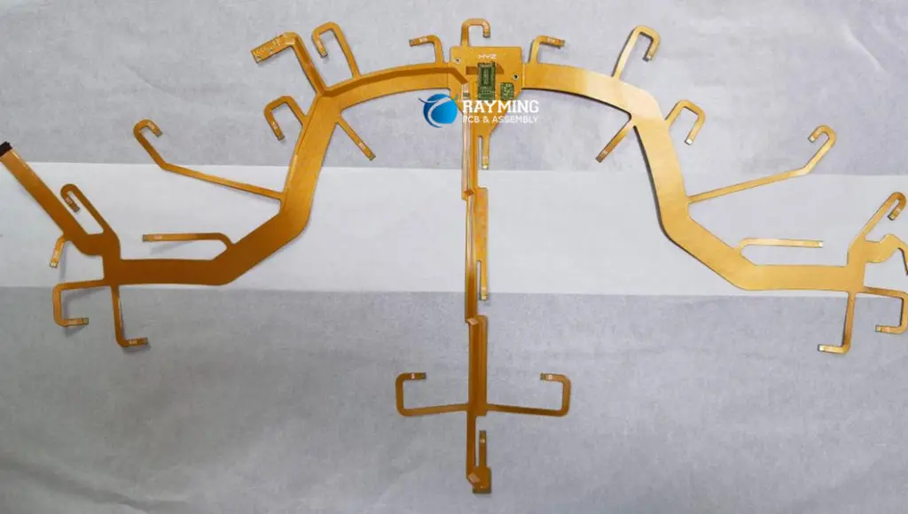
Flex PCBs are particularly susceptible to EMI due to several inherent characteristics. The thin substrate materials, typically polyimide films ranging from 12 to 125 micrometers, provide minimal natural shielding compared to thicker rigid boards. The flexible nature means that trace geometries can change during flexing, potentially altering impedance characteristics and creating impedance discontinuities that can radiate electromagnetic energy. Additionally, flex circuits often operate in close proximity to other electronic components, increasing the likelihood of coupling between circuits.

The dynamic nature of flex PCBs introduces another complexity: shield effectiveness must be maintained throughout the entire range of motion. Traditional rigid shielding solutions can crack, delaminate, or create stress concentrations that lead to failure. This dynamic environment requires shielding solutions that can accommodate repeated flexing while maintaining electrical continuity and mechanical integrity.

YouTube video

Fundamental EMI Shielding Principles for Flex Circuits

Effective EMI shielding in flex PCBs relies on three primary mechanisms: reflection, absorption, and multiple reflections. Reflection occurs at the interface between materials with different impedances, where electromagnetic waves encounter a conductive barrier. The effectiveness of reflection depends on the impedance mismatch between the wave medium and the shield material. Absorption involves the conversion of electromagnetic energy into heat as waves propagate through lossy materials. Multiple reflections occur within the shield material itself, where waves bounce between interfaces, gradually losing energy.

For flex PCBs, achieving adequate shielding effectiveness requires careful consideration of these mechanisms while maintaining flexibility. The shielding effectiveness (SE) is typically expressed in decibels and represents the ratio of incident to transmitted electromagnetic field strength. Practical flex PCB applications often require SE values ranging from 20 to 60 dB, depending on the specific application and regulatory requirements.

Material Selection for Flexible EMI Shielding

EMI shielding materials

Metallic Foils and Conductors

The choice of shielding materials significantly impacts both effectiveness and mechanical performance. Copper foil remains the most common choice due to its excellent conductivity, relatively low cost, and well-established processing techniques. However, pure copper can work-harden during repeated flexing, leading to fatigue failures. Copper alloys, particularly those containing small amounts of beryllium or phosphorus, offer improved fatigue resistance while maintaining good conductivity.

Conductive Adhesives and Bonding Materials

Conductive adhesives represent another crucial component in flex PCB shielding systems. These materials must maintain electrical continuity while accommodating the mechanical stresses associated with flexing. Silver-filled adhesives provide excellent conductivity but can be expensive and susceptible to migration issues. Copper-filled adhesives offer a good balance of performance and cost, while nickel-filled options provide moderate conductivity with enhanced durability.

Flexible Conductive Fabrics

Flexible conductive fabrics, typically consisting of metallized textile substrates, offer unique advantages for complex geometries and high-flex applications. These materials can accommodate extreme bending without losing conductivity, making them ideal for applications requiring tight bend radii or continuous flexing. The trade-off typically involves reduced shielding effectiveness compared to solid metal foils, particularly at higher frequencies.

Design Techniques for EMI Mitigation

Layer Stack-up Optimization

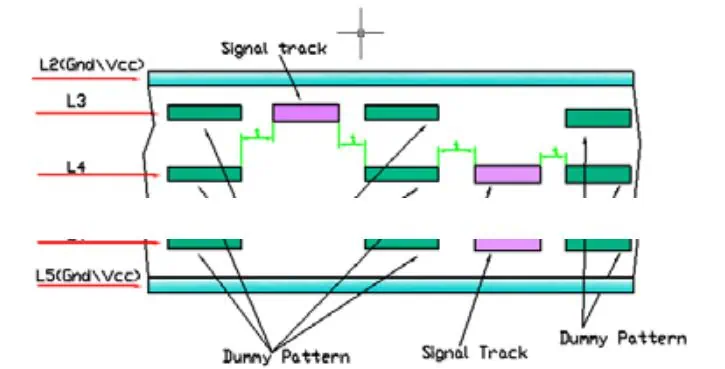
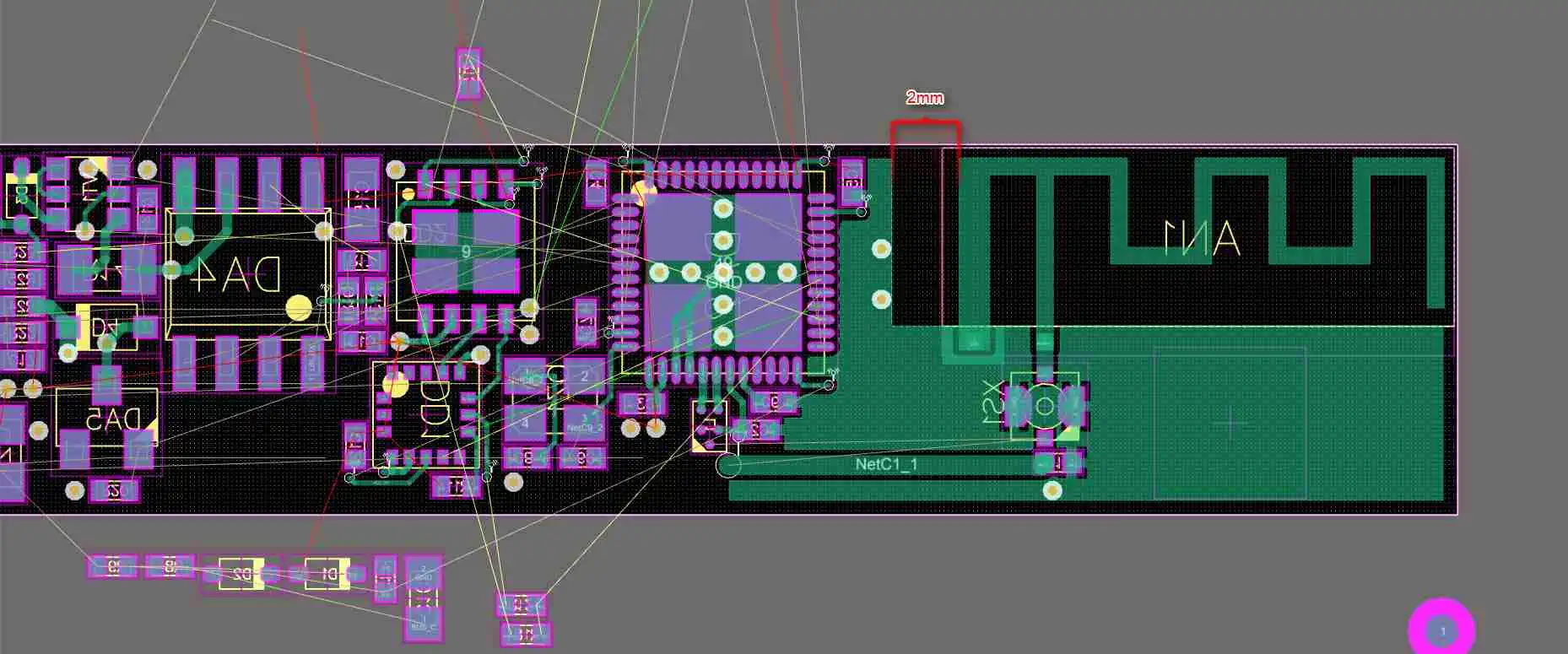
Layer stack-up optimization plays a crucial role in EMI performance. Implementing dedicated ground planes, even in thin flex constructions, significantly improves shielding effectiveness by providing a low-impedance return path for currents and creating a natural barrier to electromagnetic propagation. When thickness constraints prevent full ground planes, hatched or meshed ground patterns can provide substantial benefits while maintaining flexibility.

Trace Routing Strategies

Trace routing strategies directly impact EMI performance. Minimizing loop areas by keeping signal traces close to their return paths reduces both radiated emissions and susceptibility to external interference. Differential signaling techniques can provide inherent noise immunity while reducing the need for extensive shielding. When single-ended signals are necessary, maintaining consistent impedance and minimizing trace lengths becomes critical.

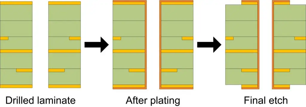
Via Design Considerations

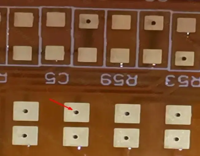
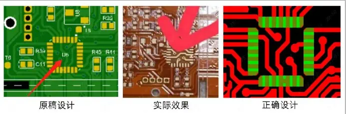
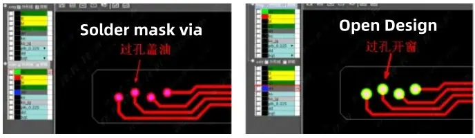
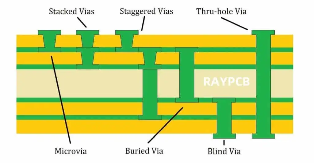
Via design in flex PCBs requires special attention for EMI control. Traditional plated through-holes can create stress concentrations during flexing, potentially compromising both mechanical integrity and electrical continuity. Alternative via technologies, such as laser-drilled microvias or conductive ink-filled vias, can provide better flex performance while maintaining EMI shielding continuity between layers.

Implementation Strategies for Flexible Shielding

Segmented Shielding Approaches

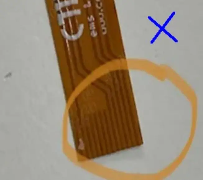
Segmented shielding approaches acknowledge that different portions of a flex circuit may have varying mechanical and EMI requirements. Static sections can utilize more robust shielding solutions, such as solid copper foils or metal-backed adhesive tapes, while dynamic flex regions employ more flexible alternatives like conductive fabrics or elastomeric shields. Careful attention to transitions between shield types ensures continuity while managing mechanical stress.

Gasket and Connector Design

Gasket and connector design significantly influences overall shielding effectiveness. Electromagnetic compatibility (EMC) gaskets must accommodate the mechanical requirements of flex circuits while maintaining reliable electrical contact. Beryllium-copper finger stock, conductive elastomers, and metallized fabric gaskets each offer distinct advantages depending on the specific application requirements.

Cable Shielding Integration

Cable shielding integration becomes particularly important when flex PCBs interface with external systems. Ensuring 360-degree shield termination prevents common-mode currents from flowing on cable shields, which can compromise overall system EMI performance. This often requires custom connector solutions or specialized cable assemblies designed specifically for flex circuit applications.

Testing and Validation Methodologies

semi-flex-pcb

EMI Testing Procedures

EMI testing for flex PCBs requires modifications to standard test procedures to account for the flexible nature of the circuits. Shielding effectiveness measurements must be performed in multiple mechanical configurations to ensure adequate performance throughout the operational range. Flexural testing combined with EMI measurements can identify potential failure modes and validate design margins.

Advanced Measurement Techniques

Near-field scanning techniques provide valuable insights into EMI performance by identifying specific areas of high electromagnetic field strength. These measurements can guide design optimization efforts and help identify unexpected coupling paths or shield discontinuities. Time-domain reflectometry (TDR) measurements can reveal impedance discontinuities that may contribute to EMI issues.

Advanced Shielding Technologies

Emerging Materials and Processes

Emerging technologies continue to expand the options for flex PCB EMI shielding. Printed conductive inks enable the direct deposition of shielding layers using standard printing processes, potentially reducing cost and complexity. These materials can be formulated to provide specific combinations of conductivity, flexibility, and adhesion properties.

Metamaterial Applications

Metamaterial concepts are being explored for EMI shielding applications, potentially offering enhanced performance at specific frequencies while maintaining mechanical flexibility. These engineered structures can provide unique electromagnetic properties not achievable with conventional materials, though practical implementation remains challenging.

Conclusion

Effective EMI shielding for flex PCBs requires a comprehensive approach that balances electromagnetic performance with mechanical requirements. Success depends on careful material selection, thoughtful design techniques, and thorough validation throughout the development process. As electronic systems continue to increase in complexity and operate at higher frequencies, the importance of robust EMI shielding strategies for flex PCBs will only continue to grow. The ongoing development of new materials and techniques promises to expand the capabilities of flexible electronics while maintaining the EMI performance required for reliable operation in increasingly challenging electromagnetic environments.

The key to successful implementation lies in understanding the fundamental trade-offs between flexibility, shielding effectiveness, and mechanical durability, then selecting the optimal combination of techniques for each specific application. With proper attention to these considerations, flex PCBs can achieve excellent EMI performance while maintaining the mechanical advantages that make them attractive for modern electronic designs.

Impedance Control of Vias and Its Influence on Signal Integrity in PCB Design

In the ever-evolving world of electronic design, the importance of signal integrity in printed circuit boards (PCBs) cannot be overstated. As clock speeds increase and signal rise times decrease, maintaining signal quality throughout the PCB becomes increasingly challenging. One critical aspect of this challenge is the impedance control of vias – the small plated holes that allow signals to transition between different layers of a multi-layer PCB.

This article delves into the intricate relationship between via impedance control and signal integrity in PCB design. We will explore the fundamentals of impedance, the role of vias in PCB design, various techniques for controlling via impedance, and the profound impact these factors have on overall signal integrity.

YouTube video

Understanding Impedance and Signal Integrity

impedance control pcb

What is Impedance?

Impedance, in the context of electrical circuits, is a measure of the opposition that a circuit presents to the flow of alternating current (AC). It is a complex quantity that includes both resistance and reactance. In PCB design, maintaining consistent impedance throughout signal paths is crucial for ensuring proper signal transmission and minimizing reflections.

Signal Integrity Basics

Signal integrity refers to the quality of an electrical signal as it travels through a PCB. Good signal integrity means that the signal arrives at its destination with minimal distortion, maintaining its original shape and timing characteristics. Factors affecting signal integrity include:

  1. Impedance mismatches
  2. Crosstalk
  3. Electromagnetic interference (EMI)
  4. Attenuation
  5. Propagation delay

The Relationship Between Impedance and Signal Integrity

Impedance control is fundamental to maintaining good signal integrity. When a signal encounters an impedance mismatch along its path, part of the signal is reflected back towards the source, causing distortions and potentially leading to errors in data transmission. By carefully controlling impedance throughout the PCB, including in vias, designers can minimize these reflections and maintain signal quality.

The Role of Vias in PCB Design

Types of Vias

Vias play a crucial role in multi-layer PCB designs, allowing signals to transition between different layers. There are several types of vias:

  1. Through-hole vias: Extend through all layers of the PCB
  2. Blind vias: Connect an outer layer to one or more inner layers
  3. Buried vias: Connect inner layers without reaching the surface
  4. Microvia: Very small vias typically used in high-density designs

Via Functions in PCB Design

Vias serve multiple purposes in PCB design:

  1. Signal routing between layers
  2. Power and ground connections
  3. Thermal management
  4. Component mounting

Challenges Associated with Vias

While vias are essential for multi-layer PCB designs, they also introduce several challenges:

  1. Impedance discontinuities
  2. Signal reflections
  3. Increased crosstalk
  4. Added capacitance
  5. Potential for manufacturing defects

Impedance Control Techniques for Vias

Differential Impedance

Controlling the impedance of vias is crucial for maintaining signal integrity in high-speed PCB designs. Several techniques can be employed to achieve this:

Via Sizing and Geometry

The size and shape of a via can significantly impact its impedance. Key factors include:

  1. Via diameter
  2. Pad size
  3. Antipad size
  4. Via length (barrel height)

Back-Drilling

Back-drilling involves removing the unused portion of a through-hole via, reducing its length and associated capacitance. This technique is particularly useful for high-speed signals on inner layers.

Via Stitching

Via stitching involves placing multiple vias in parallel to reduce the overall impedance and improve signal quality. This technique is often used for power and ground connections.

Impedance Matching Techniques

Various methods can be used to match the impedance of vias to the surrounding traces:

  1. Tapered traces leading to vias
  2. Compensation pads
  3. Stub removal

Example: Via Impedance Control Parameters

ParameterTypical RangeImpact on Impedance
Via Diameter6-20 milsSmaller diameter increases impedance
Pad Size1.5-2x via diameterLarger pad decreases impedance
Antipad Size2-3x via diameterLarger antipad increases impedance
Via LengthDepends on board thicknessLonger via increases capacitance

Impact of Via Impedance on Signal Integrity

The impedance of vias can have a significant impact on overall signal integrity in a PCB design. Some key effects include:

Signal Reflections

Impedance mismatches at vias can cause signal reflections, leading to:

  1. Ringing and overshoot
  2. Increased jitter
  3. Reduced eye diagram opening

Insertion Loss

Vias introduce additional insertion loss to the signal path, which can be particularly problematic for high-frequency signals. Factors contributing to insertion loss in vias include:

  1. Skin effect in the via barrel
  2. Dielectric losses
  3. Radiation losses

Crosstalk

Vias can act as antennas, radiating electromagnetic energy and potentially causing crosstalk with nearby signals. Proper via design and placement can help mitigate this issue.

Return Path Discontinuities

Vias can create discontinuities in the return path for high-frequency signals, leading to increased EMI and signal integrity issues.

Design Considerations for Optimal Via Performance

PCB Impedance

To ensure optimal via performance and maintain signal integrity, PCB designers should consider the following:

Via Placement Strategies

  1. Minimize the number of vias in high-speed signal paths
  2. Place vias as close as possible to the source and load
  3. Use dedicated ground vias near signal vias to maintain a consistent return path

Stackup Design

The PCB stackup plays a crucial role in via performance:

  1. Use symmetrical stackups to minimize layer transitions
  2. Maintain consistent reference planes for each signal layer
  3. Consider using buried capacitance layers for improved power integrity

Impedance Matching Techniques

  1. Use tapered traces leading to vias
  2. Implement compensation pads to match via capacitance
  3. Consider using stub removal techniques for unused via portions

Signal Routing Best Practices

  1. Route critical signals on a single layer when possible
  2. Use differential pairs for high-speed signals
  3. Maintain consistent trace widths and spacings

Advanced Techniques for Via Impedance Control

As PCB designs become more complex and operating frequencies increase, advanced techniques for via impedance control become necessary:

Coaxial Vias

Coaxial vias use a center conductor surrounded by a ground cylinder, mimicking the structure of a coaxial cable. This design provides excellent impedance control and signal isolation.

Channelized Routing

Channelized routing involves creating dedicated channels for high-speed signals, with ground vias forming walls on either side. This technique helps maintain a consistent return path and reduces crosstalk.

Landless Vias

Landless vias eliminate the pad on layers where the via doesn’t connect, reducing capacitance and improving impedance control.

Via-in-Pad Design

Via-in-pad design places vias directly in component pads, reducing the signal path length and improving performance. This technique requires careful consideration of manufacturing processes to ensure reliable solder joints.

Simulation and Modeling of Via Impedance

Accurate simulation and modeling of via impedance are crucial for optimizing PCB designs:

3D Electromagnetic Simulation

3D electromagnetic simulators can provide detailed insights into via performance, including:

  1. S-parameters
  2. Time-domain reflectometry (TDR) responses
  3. Electric and magnetic field distributions

Equivalent Circuit Models

Simplified equivalent circuit models can be used for rapid analysis of via performance:

  1. Lumped element models
  2. Transmission line models
  3. Hybrid models combining lumped elements and transmission lines

Design of Experiments (DOE) Approach

A DOE approach can be used to systematically explore the impact of various via design parameters on impedance and signal integrity.

Manufacturing Challenges and Solutions

Implementing effective via impedance control in PCB manufacturing presents several challenges:

Drill and Plating Tolerances

Variations in via diameter and plating thickness can affect impedance. Tight control of manufacturing processes is essential.

Material Considerations

The choice of PCB materials can impact via performance:

  1. Dielectric constant and loss tangent
  2. Copper foil roughness
  3. Glass weave effects

High-Aspect-Ratio Vias

Manufacturing high-aspect-ratio vias (small diameter, long length) can be challenging but is often necessary for high-layer-count boards.

Solutions and Best Practices

  1. Use of laser drilling for small, precise vias
  2. Implementation of advanced plating techniques
  3. Careful material selection and specification
  4. Regular process monitoring and control

Future Trends in Via Design and Impedance Control

impedance control in pcb

As PCB technology continues to evolve, several trends are emerging in via design and impedance control:

Advanced Materials

New PCB materials with improved electrical and thermal properties are being developed, enabling better via performance at high frequencies.

3D Printed Electronics

Additive manufacturing techniques may allow for the creation of custom-shaped vias with optimal impedance characteristics.

Optical Interconnects

As data rates continue to increase, optical interconnects may replace traditional vias for some high-speed applications.

Artificial Intelligence in PCB Design

AI-driven design tools may help optimize via placement and design for improved signal integrity.

Frequently Asked Questions

  1. Q: How does via impedance affect signal integrity in PCB design? A: Via impedance can significantly impact signal integrity by causing reflections, insertion loss, and crosstalk. Impedance mismatches at vias can lead to signal distortion, increased jitter, and reduced eye diagram opening. Proper impedance control of vias helps maintain signal quality and ensures reliable data transmission in high-speed PCB designs.
  2. Q: What are the key factors influencing via impedance? A: The main factors influencing via impedance include:
    • Via diameter
    • Pad and antipad sizes
    • Via length (barrel height)
    • PCB material properties (dielectric constant, loss tangent)
    • Surrounding ground and power planes
    • Plating thickness Careful consideration of these factors during design and manufacturing is crucial for achieving the desired via impedance.
  3. Q: How can I improve via performance in high-speed PCB designs? A: To improve via performance in high-speed PCB designs:
    • Minimize the number of vias in critical signal paths
    • Use back-drilling to remove unused via stubs
    • Implement impedance matching techniques (e.g., tapered traces, compensation pads)
    • Consider advanced techniques like coaxial vias or channelized routing
    • Use 3D electromagnetic simulation to optimize via design
    • Ensure tight manufacturing tolerances for via drilling and plating
  4. Q: What are the challenges in manufacturing high-performance vias? A: Key challenges in manufacturing high-performance vias include:
    • Maintaining tight tolerances for via diameter and plating thickness
    • Drilling and plating high-aspect-ratio vias
    • Ensuring consistent material properties across the PCB
    • Implementing advanced techniques like back-drilling or landless vias
    • Balancing performance requirements with manufacturing costs Overcoming these challenges requires close collaboration between PCB designers and manufacturers.
  5. Q: What future developments can we expect in via design and impedance control? A: Future developments in via design and impedance control may include:
    • Advanced PCB materials with improved electrical properties
    • 3D printed electronics allowing for custom via shapes
    • Integration of optical interconnects for ultra-high-speed applications
    • AI-driven design tools for optimizing via placement and performance
    • Improved simulation and modeling techniques for more accurate via characterization These advancements will enable PCB designers to create even more efficient and high-performing boards for next-generation electronic devices.

45 FPC Design Skills with Detailed graphics – Engineers Must Read | RAYMING PCB

FPC circuit

What is FPC Board?

FPC Flexible Circuit Boards are circuit boards made from a flexible substrate that is not only lightweight, but also capable of bending and folding. This design makes it useful in electronic devices with tight spaces or irregular shapes. Imagine the future of smartwatches, folding screen phones, and even wearable devices that could be thinner, lighter, more portable, and more durable thanks to FPC flexible circuit boards.

Today, from the beginner’s point of view, to bring you a comprehensive understanding of the 45 design specifications of FPC

1. Circuit design

1. large-area copper surface oxidation problem: due to the design of large-area copper surface, it is difficult to exclude the air when pressing the laminating film, and the moisture in the air under high temperature and high pressure reacts with the copper surface to oxidize, resulting in poor appearance. Although it does not affect the function, in order to avoid this problem, it is recommended to design the copper surface into a grid, or increase the solder resist window on the large copper surface.

2. Avoid designing independent pads: As shown in the figure, the line pads are designed to be independent and overlapped on both sides, and the pads are easy to come off due to the FPC intermediate substrate of only 25um. It is recommended to increase the copper cladding, and add connecting lines at the corners of the pads to connect with the copper cladding. At the same time, the top and bottom pads need to be staggered to increase the bonding force.

3. Pad off problem: Connector holder pads are easy to fall off if they are designed to be independent, it is recommended to use the pressure PAD design.

4. Large Exposed Copper Design: It is generally not recommended to design large exposed copper areas to avoid wrinkles and unevenness problems.

5. FPC board soldermask design: soft board using cover film as a soldermask, cover film need to open the window and then laminated, pad to line spacing needs to be 0.2mm or more, the width of the soldermask bridge needs to be greater than 0.5mm. if the pad spacing is less than 0.5mm, we recommend that the customer open the window, accept the production of exposed wire.

6. Anti-tear design: As shown in the picture, the row of lines is sparse and easy to tear at the corners. It is recommended to add anti-tear copper strips on the edge of the board or add mesh copper on the back.

7. Circuit grid design: Grid lines are laid at a 45-degree angle as far as possible, which is more favorable for signal transmission. Line width and line spacing is recommended to be 0.2/0.2mm.

2. FPC Shape and drilling design

  1. Distance between through-hole and plate frame line: through-hole from the plate frame line should be 0.5mm minimum, less than 0.5mm need to be changed to U-shaped hole.

2. Open Distance between the hole and the anti-soldering : the hole should be kept at least 0.2mm away from the anti-soldering to prevent the hole from exposing copper.

3. FPC board is not recommended to design the hole in the Pad, FPC is unable to do the resin plug hole, do the hole in the disk will have the risk of tin leakage.

3. Soldermask Design

  1. Connector chassis dislodgement protection: FPC connector chassis is easy to dislodge, it is recommended to use pressure PAD design.

2. Soldermask in the middle of the chip: A bridge connection is required in the middle of the chip to retain the soldermask in the middle.

3. Open desing of Gold finger pad : Gold finger pads must be soldermask Opening, otherwise it can not be connected to the connector conduction

4. Soldermask use: default use soldermask as soldermask, make sure the soldermask is correct.

5. Solder mask via hole design: In order to prevent the hole copper breakage when the hole bending, FPC holes generally do the default cover oil design. If you need to open the window, you need to make a clear note in the order!

6. Test point design: the test point is designed as an over-hole attribute resulting in no turn out, the test point can not be set as an over-hole attribute or need to add a separate open for the test point.

7. Board edges exposed copper problem: double-sided board board edges have a large area of exposed copper will lead to board edges black, it is recommended that the board edges to increase a circle of covering film.

4. Gold finger design on board edges

  1. Design of insertion and removal of gold fingers: When laser cutting, the edge of the board is carbonized by high temperature, which leads to the problem of micro-shortening between the gold fingers. It is recommended to shrink the gold fingers inward by 0.2mm.

2. Soldering finger Via-hole design: Soldering finger plate pads on the over-hole should not be designed in a row, in order to prevent stress concentration caused by fracture.

3. Soldering gold finger covering film staggered: Soldering gold finger up and down the covering film should be staggered at least 0.3mm, to prevent fracture

4. Soldering finger design: It is recommended to design for the solder resist film pressure PAD effect (i.e., the pad is extended so that the covering film presses the pad more than 0.3mm).

5. Gold finger opening desing : opening is recommended to press the soldering pad more than 0.3mm, to prevent the gold finger PAD and the connection disconnection

6. Reverse finger design: Garrigon does not support Wisps for the time being, reverse fingers need to add pads and holes to realize the layer change.

7. Pad design: FPC use solder resist film can not be like green oil as a solder resist bridge, design IC pads, pads can not have excess copper cladding, so as not to pads become larger, smaller spacing, welding is easy to short circuit.

8. Independent pad design: Gold finger pads should be designed as independent pads. If the finger pads are covered with copper and wires, the copper or wires will be exposed after the window is opened by the solder resist.

9. Goldfinger profile tolerance: Goldfinger shape tolerance is ยฑ0.1mm by default, if you require ยฑ0.05mm, you need to specify when ordering, and you need markout if you accept x-out or not.

Here is Q&A about FPC Manufacturing :

FR4 Stiffener
  1. What is the difference between hot pressing and cold pressing?
    There are two ways to laminate the reinforcement, one is to use 3M tape to directly bond, called cold pressing, the other is to use AD adhesive (thermosetting adhesive) lamination, after high temperature and high pressure to make the reinforcement and FPC tightly combined.
  2. Why thick FR4 reinforcement upgraded to hot pressing process, thin FR4 do not need hot pressing?
    A: 0.1mm and 0.2mm due to the thickness of thin, can be used ordinary fast press hot pressing, so Garrison FPC on-line is the use of hot pressing;
    0.4mm and above the thickness of FR4, due to the board height difference is large, such as the use of ordinary fast press will press the press silicone pad pressure bad, must be used in a vacuum with airbags to press the hot press.
  3. What is the difference between the internal structure of ordinary fast press and vacuum hot press?
    A: Vacuum press is more airbag, when pressing, first extract the air inside the board, and then fill the airbag with pressure gas to realize the pressing. Ordinary quick press machine is directly through the flat steel plate to realize the pressing.
  4. Thick FR4 is upgraded to hot pressing, what do I need to pay attention to on the design?
    A: Try not to make holes in the reinforcement plate corresponding to the pads to prevent the pads from being concave due to the extrusion of the air pockets during press-fit.

How to Design Elevator Button PCB

Introduction

In the world of vertical transportation, the humble elevator button panel plays a crucial role in providing a seamless and user-friendly experience for passengers. As the primary interface between the passenger and the elevator system, the design of the elevator button PCB is of paramount importance, as it directly impacts the overall functionality, reliability, and aesthetic appeal of the elevator.

Designing an elevator button PCB requires a deep understanding of various engineering principles, including electrical design, mechanical integration, and human-computer interaction. From the selection of suitable components to the optimization of the PCB layout, every aspect of the design process must be carefully considered to ensure the final product meets the stringent requirements of the elevator industry.

In this comprehensive article, we will delve into the key considerations and best practices for designing an elevator button PCB, equipping you with the knowledge and tools necessary to create a robust and efficient solution that meets the needs of both the elevator manufacturer and the end-user.

Understanding Elevator Button Panel Design

Functional Requirements

The elevator button panel is responsible for a variety of critical functions, each of which must be carefully addressed in the PCB design process. These include:

  1. Floor Selection: The primary function of the elevator button panel is to allow passengers to select their desired floor by pressing the corresponding button.
  2. Floor Indication: The panel should provide clear visual feedback to the passenger, indicating the currently selected floor or the floor the elevator is currently servicing.
  3. Accessibility Features: The button panel should incorporate accessibility features, such as Braille or tactile indicators, to accommodate passengers with visual impairments.
  4. Emergency Functionalities: The panel may also include emergency buttons, such as the “Door Open” or “Alarm” buttons, which must be designed to be easily accessible and intuitive to use.
  5. Maintenance and Diagnostics: The PCB design should facilitate maintenance and diagnostics, enabling technicians to easily identify and address any issues that may arise.

Mechanical Integration

The elevator button PCB must be seamlessly integrated with the mechanical components of the elevator, such as the door sensors, floor indicators, and the overall enclosure. This integration requires careful considerations in the areas of:

  1. Mounting and Enclosure: The PCB must be designed to fit within the designated space in the elevator’s button panel, ensuring a secure and reliable mounting solution.
  2. Button Actuation: The button design must provide a satisfying tactile feedback to the user, with proper actuation mechanisms and debouncing circuitry to prevent false triggers.
  3. Indicator Lights: The PCB must incorporate the necessary circuitry and layout to support the integration of indicator lights, such as LED-based floor indicators or emergency button status lights.
  4. Wiring and Connectors: The PCB must provide the appropriate wiring interfaces and connectors to integrate with the elevator’s control system and other peripheral components.

User Experience Considerations

The elevator button panel is the primary interface between the passenger and the elevator system, and its design must prioritize the user experience. Key considerations in this area include:

  1. Button Layout and Arrangement: The placement and arrangement of the buttons should be intuitive and ergonomic, ensuring easy access and navigation for passengers.
  2. Button Size and Spacing: The size and spacing of the buttons should be optimized to provide a comfortable and efficient user experience, considering factors such as hand size and dexterity.
  3. Visibility and Legibility: The button labels and floor indicators must be clearly visible and legible, even in low-light conditions or under various lighting environments.
  4. Accessibility and Inclusivity: The button panel design should incorporate features that cater to passengers with diverse needs, such as those with visual, physical, or cognitive impairments.
  5. Responsiveness and Feedback: The button panel should provide clear and immediate feedback to the user, such as audible or haptic responses, to confirm the successful registration of their input.

Regulatory and Safety Requirements

Elevator button panels are subject to strict regulatory and safety requirements, which must be addressed in the PCB design process. These include:

  1. Electrical Safety: The PCB must comply with relevant electrical safety standards, such as those set by the International Electrotechnical Commission (IEC) or the Underwriters Laboratories (UL).
  2. Accessibility Standards: The button panel design must adhere to accessibility guidelines, such as the Americans with Disabilities Act (ADA) or the EN 81-70 standard in Europe, to ensure inclusivity.
  3. Fire and Vandalism Protection: The PCB and its enclosure should be designed to withstand potential fire hazards and vandalism, ensuring the continued safe operation of the elevator.
  4. Electromagnetic Compatibility: The PCB layout and circuitry must be designed to comply with electromagnetic compatibility (EMC) standards, minimizing the risk of interference with other electronic systems in the elevator.
  5. Environmental Resilience: The PCB must be able to withstand the environmental conditions commonly found in elevator shafts, such as temperature extremes, humidity, and vibrations.

Key Considerations in Elevator Button PCB Design

Component Selection

The selection of the appropriate components for an elevator button PCB is a critical step in the design process, as it directly impacts the overall performance, reliability, and cost-effectiveness of the final product.

Key Factors in Component Selection

  1. Button Switches: The choice of button switches, such as tactile, membrane, or capacitive touch, should be based on factors like longevity, tactile feedback, and ease of integration.
  2. Indicator Lights: The selection of indicator lights, typically LEDs, should consider factors like brightness, color, and power consumption.
  3. Microcontroller: The microcontroller used to manage the button panel’s functionality should have the necessary processing power, memory, and connectivity options to support the design requirements.
  4. Power Supply: The power supply circuitry, including voltage regulators and power management ICs, must be designed to provide stable and reliable power to all the components on the PCB.
  5. Connectors and Interfaces: The selection of appropriate connectors and interfaces, such as ribbon cables or terminal blocks, should ensure a seamless integration with the elevator’s control system.
  6. Environmental Resistance: The selection of components should prioritize those with the necessary environmental resilience to withstand the conditions commonly found in elevator shafts, such as temperature extremes, humidity, and vibrations.

PCB Layout and Design

The layout and design of the elevator button PCB play a crucial role in ensuring the overall functionality, reliability, and manufacturability of the final product.

Key Considerations in PCB Layout and Design

  1. Button Arrangement and Spacing: The layout of the buttons should be carefully planned to provide an intuitive and ergonomic user experience, with proper spacing and alignment.
  2. Indicator Light Placement: The placement of the indicator lights, such as floor indicators or emergency button status lights, should be optimized for maximum visibility and legibility.
  3. Power Distribution: The PCB layout should incorporate efficient power distribution, with dedicated power and ground planes to ensure stable and reliable power delivery to all the components.
  4. Signal Routing: The routing of signals, such as button inputs and indicator light controls, should be designed to minimize electromagnetic interference (EMI) and maintain signal integrity.
  5. Heat Management: The PCB layout should consider the heat generated by the components, such as the microcontroller and indicator lights, and incorporate features to ensure proper heat dissipation.
  6. Mechanical Integration: The PCB layout should be designed to seamlessly integrate with the mechanical components of the elevator button panel, including the enclosure, mounting points, and wiring harnesses.
  7. Manufacturability and Testability: The PCB layout should be optimized for ease of manufacturing and testing, ensuring a cost-effective and reliable production process.

Microcontroller and Firmware Design

The microcontroller is the heart of the elevator button PCB, responsible for managing the various functionalities and ensuring the smooth operation of the button panel.

Key Aspects of Microcontroller and Firmware Design

  1. Button Scanning and Debouncing: The firmware should implement efficient button scanning algorithms and debouncing mechanisms to accurately detect and register user inputs.
  2. Indicator Light Control: The firmware should provide the necessary control and management of the indicator lights, ensuring proper signaling and feedback to the user.
  3. Communication and Integration: The firmware should handle the communication protocols and interfaces required to integrate the button panel with the elevator’s control system, enabling seamless data exchange and coordination.
  4. Diagnostics and Maintenance: The firmware should incorporate features to facilitate diagnostics and maintenance, such as error logging, status reporting, and remote firmware updates.
  5. Power Management: The firmware should implement power management strategies to optimize energy efficiency and ensure reliable operation, even in the event of power fluctuations or outages.
  6. Accessibility Features: The firmware should support accessibility features, such as Braille or audible cues, to enhance the usability of the button panel for passengers with diverse needs.
  7. Fail-Safe Mechanisms: The firmware should incorporate fail-safe mechanisms to ensure the continued safe operation of the elevator in the event of a button panel failure or malfunction.

Electrical Design Considerations

The electrical design of the elevator button PCB is essential for ensuring the proper functionality, safety, and reliability of the overall system.

Key Electrical Design Considerations

  1. Power Supply: The design of the power supply circuitry, including voltage regulators, power management ICs, and decoupling capacitors, should provide stable and reliable power to all the components on the PCB.
  2. Button Input Circuitry: The button input circuitry should be designed to accurately detect and debounce user inputs, preventing false triggers and ensuring reliable floor selection.
  3. Indicator Light Driving: The circuitry responsible for driving the indicator lights, such as LEDs, should be designed to provide the necessary current and voltage levels while considering power consumption and heat dissipation.
  4. Electromagnetic Compatibility (EMC): The electrical design should address EMC concerns, incorporating features like EMI filtering, shielding, and proper grounding to minimize interference with other electronic systems in the elevator.
  5. Circuit Protection: The inclusion of circuit protection mechanisms, such as overcurrent protection, ESD protection, and transient voltage suppression, can help safeguard the PCB and its components against various electrical hazards.
  6. Wiring and Interconnects: The design of the wiring and interconnects between the button panel PCB and the elevator’s control system should ensure reliable data and signal transmission, as well as ease of installation and maintenance.
  7. Regulatory Compliance: The electrical design of the PCB must comply with relevant safety standards and regulations, such as those set by the IEC or UL, to ensure the overall safety and reliability of the elevator system.

Mechanical Integration and Enclosure Design

The successful integration of the elevator button PCB with the mechanical components and the overall enclosure design is crucial for achieving a seamless and robust solution.

Key Aspects of Mechanical Integration and Enclosure Design

  1. Enclosure Design: The enclosure design should provide the necessary protection for the PCB, including environmental sealing, impact resistance, and ease of access for maintenance and servicing.
  2. Button Actuation Mechanism: The design of the button actuation mechanism, including the button stems, springs, and tactile feedback mechanisms, should ensure a positive and reliable user experience.
  3. Mounting and Alignment: The PCB should be designed for secure and reliable mounting within the elevator button panel, ensuring proper alignment with the enclosure and other mechanical components.
  4. Wiring and Connectivity: The PCB design should incorporate appropriate wiring interfaces and connectors to facilitate the seamless integration with the elevator’s control system and other peripheral components.
  5. Accessibility and Inclusivity: The mechanical design of the button panel should consider accessibility features, such as Braille markings or raised tactile indicators, to accommodate passengers with diverse needs.
  6. Aesthetics and Ergonomics: The overall design of the button panel, including the integration of the PCB, should prioritize a visually appealing and ergonomic user experience.
  7. Manufacturability and Serviceability: The mechanical design should consider the ease of manufacturing, assembly, and servicing, ensuring a cost-effective and maintainable solution.

Quality Assurance and Testing

Ensuring the quality and reliability of the elevator button PCB is of paramount importance, as the performance and safety of the elevator system depend on the integrity of this critical component.

Key Quality Assurance and Testing Considerations

  1. Component-Level Testing: Rigorous testing of individual components, such as button switches, indicator lights, and the microcontroller, should be performed to verify their functionality and compliance with specifications.
  2. Functional Testing: Comprehensive functional testing of the complete button panel, including button input, indicator light operation, and integration with the elevator control system, should be carried out to ensure the overall system performs as intended.
  3. Environmental Testing: The PCB and the entire button panel assembly should be subjected to environmental testing, such as temperature cycling, humidity, and vibration testing, to validate their resilience and durability under the expected operating conditions.
  4. Electrical Safety Testing: Electrical safety testing, in accordance with relevant standards, should be performed to ensure the PCB and the button panel meet the required safety regulations and protect users from potential electrical hazards.
  5. Electromagnetic Compatibility (EMC) Testing: EMC testing should be conducted to verify that the button panel PCB, and the overall elevator system, do not generate or are not susceptible to electromagnetic interference that could compromise the system’s operation.
  6. Reliability Testing: Long-term reliability testing, such as accelerated life testing and failure mode analysis, should be performed to assess the button panel’s durability and identify potential failure modes.
  7. Compliance and Certification: The button panel design and its associated testing should be aligned with relevant industry standards and regulations, ensuring the product can be certified and approved for safe and legal use in elevator installations.

Optimization Techniques for Elevator Button PCB Design

Design for Manufacturability (DFM)

Designing the elevator button PCB with a focus on manufacturability is crucial to ensure the cost-effectiveness and scalability of the production process.

Key DFM Considerations

  1. Component Placement and Orientation: The placement and orientation of components on the PCB should be optimized for efficient pick-and-place assembly.
  2. Trace Routing and Clearances: The trace routing and clearances on the PCB should be designed to accommodate the capabilities of the manufacturing process, such as minimum trace widths and spacing.
  3. Assembly Processes: The PCB design should be compatible with the intended assembly processes, such as surface mount technology (SMT) or through-hole soldering, to ensure reliable and cost-effective production.
  4. Test Points and Accessibility: The PCB layout should provide easy access to test points and critical components, facilitating efficient testing and debugging during the manufacturing process.
  5. Standardization and Modularization: Adopting a standardized design approach and modular architecture can help streamline the manufacturing process and enable scalability.
  6. Collaboration with Manufacturers: Close collaboration with the PCB manufacturer can help identify design optimizations that leverage their expertise and production capabilities.

Thermal Management Optimization

Effective thermal management is crucial for the reliable and long-term operation of the elevator button PCB, as the components, particularly the indicator lights and the microcontroller, can generate significant amounts of heat during operation.

Thermal Management Strategies

  1. Heatsink Integration: Designing the PCB layout to facilitate the integration of a dedicated heatsink or heat spreader can significantly improve heat dissipation.
  2. Thermal Vias and Copper Planes: The strategic placement of thermal vias and the utilization of copper planes can enhance heat transfer from heat-generating components to the surrounding layers and the heatsink.
  3. Component Placement and Orientation: Carefully considering the placement and orientation of heat-generating components, such as the microcontroller and indicator lights, can optimize airflow and heat dissipation.
  4. Thermal Simulation and Analysis: The use of thermal simulation tools and analysis techniques can help identify potential hot spots and guide the optimization of the PCB layout for effective heat dissipation.
  5. Material Selection: The choice of materials, such as the dielectric layers and the copper weight, can impact the thermal performance of the PCB and the overall thermal management of the elevator button panel.

Electromagnetic Interference (EMI) Mitigation

Electromagnetic interference (EMI) is a critical concern in the design of the elevator button PCB, as it can impact the overall system performance, reliability, and compliance with regulatory standards.

EMI Mitigation Techniques

  1. Power Supply and Decoupling: Proper power supply design and the use of decoupling capacitors can help mitigate conducted EMI issues.
  2. Trace Design and Routing: The design and routing of traces, particularly for high-speed signals, can impact radiated EMI and signal integrity.
  3. Grounding and Shielding: The use of ground planes, ground vias, and shielding can help contain and suppress electromagnetic interference.
  4. Component Placement: The placement and orientation of components, especially high-speed digital and power electronics, can affect EMI performance.
  5. Simulation and Testing: Electromagnetic simulation tools and EMI testing during the design process can help identify and address potential issues early on.

Cost Optimization

In addition to the technical performance requirements, the design of the elevator button PCB must also consider the overall cost-effectiveness of the solution to ensure commercial viability.

Cost Optimization Strategies

  1. Component Selection: The choice of components, such as the button switches, indicator lights, and the microcontroller, can significantly impact the overall cost of the PCB.
  2. PCB Complexity: Simplifying the PCB design, in terms of the number of layers and the component density, can help reduce manufacturing costs.
  3. **Standardization and

Inexpensive PCB Prototyping: Compare Prices & Save on Your Next Project

PCB prototype assembly suppliers

In today’s fast-paced world of electronics, printed circuit boards (PCBs) are the backbone of nearly every electronic device. Whether you’re a hobbyist, a startup, or an established company, understanding and managing PCB prototype costs is crucial for successful project development. This comprehensive guide will walk you through everything you need to know about PCB prototyping costs, helping you make informed decisions and save money on your next project.

Understanding PCB Prototype Costs

Before diving into cost-saving strategies, it’s essential to understand what factors influence PCB prototype costs. By grasping these elements, you’ll be better equipped to make cost-effective decisions without compromising quality.

Factors Affecting PCB Prototype Cost

  1. Board Size: The physical dimensions of your PCB directly impact the cost. Larger boards require more materials and processing time, increasing the overall expense.
  2. Layer Count: Single-layer boards are the most economical, while multi-layer boards increase in cost with each additional layer. Complex designs often require multiple layers, balancing functionality with cost.
  3. Material Selection: The choice of substrate material affects both performance and price. FR-4 is a common, cost-effective option, while specialized materials like Rogers or polyimide can significantly increase costs.
  4. Copper Weight: Thicker copper layers are more expensive but may be necessary for high-current applications or improved heat dissipation.
  5. Surface Finish: Different finishes like HASL, ENIG, or immersion gold offer varying levels of protection and solderability at different price points.
  6. Minimum Trace Width and Spacing: Tighter tolerances require more advanced manufacturing processes, increasing costs.
  7. Drill Hole Density: More holes per square inch require more time and specialized equipment, driving up the price.
  8. Quantity: Economies of scale apply to PCB production. Ordering larger quantities can reduce the per-unit cost, but may not always be practical for prototyping.
  9. Turnaround Time: Expedited services come at a premium. Standard production times are more economical but require patience.

Strategies for Reducing PCB Prototype Costs

Now that we understand the factors influencing PCB prototype costs, let’s explore strategies to minimize expenses without sacrificing quality or functionality.

1. Optimize Your Design

Efficient design is the foundation of cost-effective PCB prototyping. Consider the following tips:

  • Minimize Board Size: Compact designs not only save on material costs but can also improve electrical performance.
  • Reduce Layer Count: Challenge yourself to accomplish your design goals with fewer layers when possible.
  • Standardize Components: Using common, readily available components can reduce overall costs and improve manufacturability.

2. Choose Materials Wisely

While high-performance materials have their place, they’re not always necessary for prototyping. Consider these material choices:

  • Stick with FR-4: For most prototypes, standard FR-4 is sufficient and cost-effective.
  • Evaluate Copper Weight: 1 oz copper is adequate for many applications and is less expensive than thicker options.
  • Select Economical Surface Finishes: HASL (Hot Air Solder Leveling) is often the most budget-friendly option for prototypes.

3. Leverage Design for Manufacturing (DFM) Principles

Adhering to DFM guidelines can significantly reduce manufacturing costs and improve yield:

  • Use Standard Drill Sizes: Avoid specifying odd-sized holes that require special drill bits.
  • Maintain Reasonable Trace Widths: Wider traces are easier and cheaper to manufacture than extremely thin ones.
  • Consider Panelization: For smaller boards, panelizing multiple designs can reduce costs.

4. Explore Different Manufacturers

PCB prototype costs can vary significantly between manufacturers. Consider the following when choosing a supplier:

  • Compare Quotes: Get quotes from multiple manufacturers to find the best balance of cost, quality, and service.
  • Look for Bundled Services: Some manufacturers offer design review, assembly, and testing services that can be more cost-effective than using separate vendors.
  • Consider Overseas Options: While domestic manufacturers may offer faster turnaround times, overseas suppliers often provide lower costs for those with flexible timelines.

5. Optimize Order Quantities

Finding the sweet spot in order quantity can lead to significant savings:

  • Evaluate Minimum Order Quantities: Some manufacturers offer better rates for slightly larger orders. Calculate if ordering a few extra boards could reduce your per-unit cost.
  • Plan for Future Iterations: Consider ordering extra boards to account for potential design revisions, which can be more cost-effective than placing multiple small orders.

Read more about:

Advanced Techniques for PCB Prototype Cost Reduction

For those looking to further optimize their PCB prototype costs, consider these advanced strategies:

1. Embrace Open-Source Tools

Utilizing open-source PCB design software can significantly reduce upfront costs:

  • KiCad: A powerful, free PCB design suite that rivals many commercial offerings.
  • FreePCB: Another free option suitable for simpler designs.
  • Eagle (Free Version): While limited in board size and layers, it’s sufficient for many prototype projects.

2. Participate in Group Orders

Some online communities and PCB manufacturers offer group ordering services:

  • PCB Prototyping Services: Platforms like PCBWay and JLCPCB sometimes offer group buy options.
  • Maker Communities: Join maker spaces or online forums where members sometimes organize group PCB orders.

3. Consider Flex PCB Alternatives

For certain applications, flexible PCBs might be a cost-effective alternative:

  • Reduced Assembly Costs: Flex PCBs can eliminate the need for connectors and wiring in some designs.
  • Space Savings: In compact designs, flex PCBs can reduce overall product size and complexity.

4. Leverage Additive Manufacturing

For extremely low volume or highly iterative prototyping, consider additive manufacturing techniques:

  • 3D Printed Electronics: While not suitable for all applications, 3D printed circuits can be incredibly cost-effective for certain prototypes.
  • Conductive Ink Printing: Another emerging technology that can be useful for quick, low-cost prototyping of simple circuits.

Balancing Cost and Quality in PCB Prototyping

Rogers RO4500 PCB

While reducing PCB prototype costs is important, it’s crucial to maintain a balance between cost-saving measures and the quality required for your project. Here are some considerations:

1. Identify Critical Components

Not all parts of your PCB design require the same level of precision or quality:

  • High-Speed Sections: Areas with high-frequency signals may require better materials or tighter tolerances.
  • Power Distribution: Sections handling high currents might need thicker copper or special considerations.
  • Standard Interfaces: Areas with standard connectors or low-speed signals can often use more economical manufacturing options.

2. Invest in Design Verification

Spending a bit more on design verification can save significant costs in the long run:

  • Simulation Software: Tools like SPICE can help identify potential issues before manufacturing.
  • DFM Checks: Many PCB design software packages include DFM checks that can catch costly errors early.
  • Professional Review: For critical projects, investing in a professional design review can be well worth the cost.

3. Consider the Entire Product Lifecycle

When evaluating PCB prototype costs, consider the entire product development cycle:

  • Iterative Prototyping: Sometimes, investing in multiple, less expensive prototype runs can be more cost-effective than trying to perfect the design in one expensive iteration.
  • Scalability: Ensure your prototype design can be easily scaled for production without requiring major changes.
  • Long-term Reliability: Cutting costs on critical components or processes might lead to reliability issues that are more expensive to fix later.

Conclusion: Mastering PCB Prototype Costs

Successfully managing PCB prototype costs requires a multifaceted approach. By understanding the factors that influence costs, implementing smart design strategies, and leveraging cost-saving techniques, you can significantly reduce your PCB prototyping expenses without compromising on quality or functionality.

Remember, the goal of prototyping is to validate your design and identify potential issues early in the development process. While cost is an important factor, it shouldn’t come at the expense of achieving these primary objectives.

By applying the strategies and insights shared in this guide, you’ll be well-equipped to navigate the world of PCB prototyping, making informed decisions that balance cost, quality, and performance. Whether you’re working on a hobby project, a startup innovation, or a corporate product development initiative, mastering PCB prototype costs will give you a competitive edge and help bring your electronic designs to life more efficiently and economically.

As you embark on your next PCB prototyping project, remember that each design presents unique challenges and opportunities for cost optimization. Stay curious, keep learning, and don’t hesitate to experiment with different approaches. With persistence and smart decision-making, you’ll find the perfect balance between cost-effectiveness and performance for your PCB prototypes.

Flexible PCB Manufacturing in Canada: Fast Prototyping & Low-Cost Production

Flexible Printed Circuit Board Manufacturers

In today’s rapidly evolving electronics landscape, flexible printed circuit boards (flex PCBs) have become essential components for innovative product design. Sourcing these vital components from Canadian manufacturers offers significant advantages for businesses seeking quality, speed, and cost-effectiveness. This comprehensive guide explores why flex PCB Canada suppliers are increasingly becoming the preferred choice for companies needing reliable prototyping and production solutions.

Understanding Flexible PCBs and Their Applications

What Exactly Is a Flexible PCB?

Flexible PCBs are circuit boards manufactured using pliable materials that allow them to bend, fold, and conform to three-dimensional shapes. Unlike traditional rigid PCBs, flex PCBs utilize thin, flexible substrate materialsโ€”typically polyimide or polyester filmsโ€”that maintain electrical connectivity while accommodating movement and vibration. This fundamental difference enables product designs that would be impossible with conventional rigid boards.

The core structure of a flex PCB typically includes:

  • A flexible polyimide base material (most commonly Kaptonยฎ)
  • Conductive copper traces for electrical pathways
  • Protective coverlay or solder mask layers
  • Various surface finish options (ENIG, immersion tin, etc.)

These specialized circuit boards can range from simple single-sided designs to complex multi-layer configurations, depending on the application requirements.

Critical Applications Across Industries

The versatility of flex PCBs has made them indispensable across numerous sectors:

Medical Devices: Canadian-manufactured flex PCBs power life-saving medical equipment where reliability is non-negotiable. From hearing aids and pacemakers to wearable health monitors, these flexible circuits enable miniaturization while maintaining durability in critical applications.

Automotive Electronics: Modern vehicles incorporate dozens of flex PCBs in dashboard displays, engine management systems, and advanced driver assistance systems (ADAS). The ability to withstand vibration, temperature fluctuations, and tight space constraints makes flex PCBs ideal for automotive applications.

Aerospace and Defense: Canadian flex PCB manufacturers support the aerospace industry with lightweight, reliable circuits for satellite systems, aircraft instrumentation, and defense applications where failure is not an option.

Consumer Electronics: Smartphones, tablets, digital cameras, and wearable technology all depend on flex PCBs to achieve their sleek, compact designs while maintaining functionality.

Why Flexibility Matters in Modern Electronics

The demand for flex PCB Canada solutions continues to grow because flexibility offers distinct advantages:

  • Space Optimization: Flex PCBs can fold into compact spaces, enabling 3D packaging that reduces overall device size.
  • Weight Reduction: Critical for aerospace and portable electronics, flex PCBs are significantly lighter than rigid alternatives.
  • Dynamic Applications: Components that must withstand repeated bending or movement during operation require flexible circuits.
  • Improved Reliability: Fewer connectors mean fewer potential points of failure, enhancing overall system reliability.
  • Thermal Management: Flexible circuits can distribute heat more effectively across confined spaces.

Advantages of Choosing Flex PCB Manufacturing in Canada

Quality Standards and Regulatory Compliance

Canadian flex PCB manufacturers operate under stringent quality control systems and regulatory frameworks. Most maintain ISO 9001 certification at minimum, with many also holding specialized certifications for aerospace (AS9100), automotive (IATF 16949), and medical device (ISO 13485) manufacturing.

This commitment to quality translates into several tangible benefits:

  • Consistent manufacturing processes with documented quality controls
  • Regular third-party audits ensuring compliance
  • Traceability of materials and processes
  • Lower defect rates and higher reliability
  • Adherence to international standards like IPC-6013 for flexible circuits

Geographic Proximity and Communication Benefits

For North American companies, partnering with a flex PCB Canada manufacturer offers significant practical advantages:

  • Time Zone Alignment: Real-time communication during standard business hours
  • Reduced Language Barriers: Clear technical discussions without misinterpretations
  • Shorter Shipping Distances: Faster delivery times and lower shipping costs
  • Easier Site Visits: The ability to visit manufacturing facilities for critical projects
  • Cultural Business Alignment: Similar business practices and expectations

Intellectual Property Protection

Intellectual property protection represents another crucial advantage of manufacturing flex PCBs in Canada. Canadian laws provide robust IP safeguards, giving businesses confidence that their proprietary designs and technologies remain secure throughout the manufacturing process.

Fast Prototyping Capabilities for Flexible PCBs in Canada

Accelerating the Design-to-Production Cycle

Canadian flex PCB manufacturers have developed streamlined processes specifically for rapid prototyping. These accelerated services typically include:

  • Online quoting systems for instant pricing
  • Design for manufacturability (DFM) reviews within 24 hours
  • Expedited material procurement for common substrates
  • Dedicated prototyping lines separate from volume production
  • Advanced digital manufacturing techniques

The result is a significantly compressed timeline from concept to functional prototype, with many Canadian suppliers offering turnaround times as quick as 3-5 business days for standard flex PCB prototypes.

Typical Lead Times for Canadian Flex PCB Prototyping

Lead times vary based on design complexity, but general expectations include:

  • Simple single-sided flex PCBs: 3-5 business days
  • Double-sided flex PCBs: 5-7 business days
  • Multi-layer flex circuits: 7-10 business days
  • Rigid-flex hybrid designs: 10-15 business days

These timelines represent a substantial improvement over offshore manufacturing options that often require 3-4 weeks for comparable prototyping services.

Iterative Design Support

Beyond speed, Canadian flex PCB manufacturers typically offer enhanced engineering support during the prototyping phase. This collaborative approach includes:

  • Design optimization suggestions
  • Material recommendations based on application requirements
  • Manufacturability enhancements
  • Testing and validation services
  • Rapid iteration capabilities for design refinements

This level of support proves invaluable for companies developing innovative products with tight market windows.

Read more about:

Cost-Effective Flex PCB Production in Canada

Long-Term Value Proposition

While unit costs for flex PCBs manufactured in Canada may initially appear higher than overseas alternatives, the total cost of ownership often proves more favorable when considering all factors:

  • Reduced Quality Issues: Lower defect rates mean fewer costly reworks and field failures
  • Faster Time-to-Market: Compressed development cycles translate to earlier revenue generation
  • Inventory Management: Shorter lead times allow for leaner inventory practices
  • Supply Chain Resilience: Reduced vulnerability to international shipping disruptions
  • Simplified Logistics: Lower shipping costs and fewer customs complications

Balancing Quality with Affordability

Canadian flex PCB manufacturers have implemented several strategies to remain cost-competitive while maintaining quality:

  • Advanced automation reducing labor costs
  • Lean manufacturing principles minimizing waste
  • Strategic material sourcing and inventory management
  • Specialized equipment optimized for flexible circuit production
  • Energy efficiency initiatives reducing overhead costs

Volume Production Economics

As production volumes increase, Canadian manufacturers offer increasingly competitive pricing structures:

  • Volume discount tiers beginning at modest quantities (often 100+ units)
  • Panel optimization for higher-volume runs
  • Material quantity discounts passed through to customers
  • Dedicated production cells for recurring orders
  • Just-in-time delivery options reducing inventory carrying costs

For many companies, the sweet spot for Canadian flex PCB manufacturing lies in low to medium production volumes (100-10,000 units), where quality, speed, and total cost align optimally.

Essential Selection Criteria for Flex PCB Manufacturers in Canada

Technical Capabilities Assessment

When evaluating potential flex PCB Canada partners, consider these technical capabilities:

  • Layer Count Capacity: Maximum number of layers they can reliably produce
  • Minimum Feature Sizes: Trace width/spacing limitations and via technology
  • Material Options: Range of base materials, adhesives, and surface finishes available
  • Special Processes: Capabilities for selective stiffeners, shielding, or embedded components
  • Testing Infrastructure: In-house electrical testing capabilities and quality verification

Certifications and Standards

Look for manufacturers maintaining relevant certifications:

  • ISO 9001 (Quality Management)
  • ISO 13485 (Medical Devices)
  • AS9100 (Aerospace)
  • IATF 16949 (Automotive)
  • IPC Member certification
  • UL certification for materials

Design Support Services

Evaluate the manufacturer’s ability to support your design process:

  • Design rule checking and optimization
  • Material selection guidance
  • Stack-up recommendations
  • Design for manufacturing (DFM) reviews
  • Design for testing (DFT) strategies

Customer Experience Factors

Beyond technical capabilities, consider these operational factors:

  • Communication responsiveness
  • Project management processes
  • Online ordering and tracking systems
  • Documentation and traceability
  • Technical support availability

Emerging Trends in Flex PCB Technology in Canada

Material and Manufacturing Innovations

Canadian flex PCB manufacturers are advancing the field through several innovations:

  • Ultra-Thin Substrates: Development of reliable circuits using substrates under 25ฮผm
  • Embedded Components: Integrating passive and active components within the flex layers
  • Advanced Adhesiveless Laminates: Improving thermal performance and reliability
  • Additive Manufacturing: Exploring printed electronics for specialized applications
  • Green Manufacturing: Reducing environmental impact through material and process improvements

Growing Demand Across Canadian Industries

Several sectors are driving increased demand for flex PCB Canada solutions:

  • Clean Energy Technologies: Solar panels, wind turbines, and battery management systems
  • IoT Devices: Smart home technology, industrial sensors, and connected infrastructure
  • Advanced Manufacturing: Robotics, automation systems, and smart factories
  • Digital Health: Wearable medical devices and remote monitoring solutions

Canadian manufacturers are well-positioned to support these growth areas with specialized flex PCB capabilities.

Integration with Advanced Electronics

The future of flex PCB development in Canada includes deeper integration with:

  • Microelectromechanical Systems (MEMS): Combining flex PCBs with tiny mechanical elements
  • Printed Electronics: Incorporating printed components directly onto flexible substrates
  • Advanced Interconnect Technologies: Developing high-density, reliable connections between flex and rigid elements
  • 5G and RF Applications: Specialized flex PCBs optimized for high-frequency performance

Conclusion: Making the Right Choice for Flex PCB Canada Manufacturing

The Canadian flexible PCB manufacturing landscape offers compelling advantages for companies seeking reliable, high-quality circuit solutions with fast turnaround times. By balancing quality, speed, and cost-effectiveness, Canadian manufacturers provide a valuable alternative to overseas production, particularly for prototyping and low to medium volume requirements.

When selecting a flex PCB Canada partner, conduct thorough due diligence on their technical capabilities, quality systems, and support services. The right manufacturing relationship can significantly enhance your product development process and contribute to market success.

To begin exploring Canadian flex PCB manufacturing options, request quotes from several qualified suppliers, review their capabilities against your specific requirements, and consider starting with a prototype project to evaluate their performance firsthand.

Frequently Asked Questions

Q: What is the typical turnaround time for flex PCB prototypes in Canada?
A: Most Canadian manufacturers can deliver simple flex PCB prototypes in 3-7 business days, with more complex designs requiring 7-15 business days.

Q: Are Canadian-manufactured flex PCBs more expensive than Asian alternatives?
A: While unit costs may be higher, the total cost of ownership often favors Canadian manufacturing when considering quality, lead time, shipping, and support factors.

Q: What minimum feature sizes can Canadian flex PCB manufacturers achieve?
A: Leading Canadian manufacturers can typically achieve trace/space widths down to 3mil/3mil (0.076mm) and via holes as small as 0.2mm.

Q: Can Canadian manufacturers handle both prototyping and volume production?
A: Yes, most established Canadian flex PCB manufacturers offer seamless scaling from prototype to production volumes, with optimal economics in the low-to-medium volume range.

Q: What design file formats do Canadian flex PCB manufacturers accept?
A: Most accept standard industry formats including Gerber files, ODB++, and native CAD files from common design platforms like Altium, Eagle, and OrCAD.

Improving Yield and Reliability in PTH Vias Drilling and Plating Processes

Plated through-hole (PTH) vias and standard vias are both conductive holes in a PCB, but they serve different purposes.

Aย plated through-hole (PTH)ย is a drilled hole that extends through the entire board and is electroplated with conductive material (typically copper) to form an electrical connection between layers. These holes are often used forย component leads (through-hole technology)ย or asย interlayer connectionsย in multilayer PCBs.

In contrast, a via (blind, buried, or microvia) is a smaller conductive hole that connects specific layers without passing through the entire board. While all PTHs are technically vias, not all vias are PTHsโ€”the key distinction lies in their function and structure.

YouTube video

What are PTH Vias?

PTH vias, or Plated Through-Hole vias, are conductive pathways that connect different layers of a multilayer printed circuit board. These cylindrical structures are created by drilling holes through the PCB and then plating the inner walls with conductive material, typically copper. PTH vias serve as electrical connections between the various layers of the board, allowing signals and power to flow seamlessly throughout the entire circuit.

Types of PTH Vias

There are several types of PTH vias, each serving a specific purpose in PCB design:

  1. Through-hole vias: These extend through all layers of the PCB and are used for component leads and interconnections.
  2. Blind vias: Visible on one side of the board, these connect an outer layer to one or more inner layers.
  3. Buried vias: These are hidden within the inner layers of the PCB and connect two or more internal layers.

Importance of PTH Vias in PCB Manufacturing

PTH vias play a crucial role in modern electronics, offering several advantages that make them indispensable in PCB manufacturing:

Enhanced Connectivity

PTH vias enable complex routing schemes by allowing signals to pass between multiple layers of a PCB. This capability is essential for creating high-density circuit designs with optimal signal integrity.

Improved Thermal Management

By providing additional pathways for heat dissipation, PTH vias contribute to better thermal management in electronic devices. This is particularly important in high-power applications where heat buildup can lead to performance issues or component failure.

Increased Mechanical Strength

The plated walls of PTH vias add structural integrity to the PCB, reinforcing the connection between layers and improving the overall durability of the board.

Space Optimization

PTH vias allow for more efficient use of PCB real estate by enabling designers to route signals vertically through the board, reducing the need for extensive surface-level routing.

Read more about:

Common Defects in PTH Via Manufacturing

Despite their importance, PTH vias are susceptible to various defects that can compromise the reliability and performance of the PCB. Some common issues include:

Drill Smear

Drill smear occurs when the heat generated during the drilling process causes resin from the PCB material to melt and coat the inner walls of the via. This can prevent proper plating and lead to poor electrical connections.

Voids in Plating

Incomplete or inconsistent plating can result in voids within the via walls. These voids can cause open circuits or intermittent connections, leading to device failure.

Resin Recession

Resin recession happens when the PCB material around the via shrinks during the thermal cycling process, creating a gap between the plating and the board material. This can result in reliability issues and potential device failure.

Copper Wrap Plating Defects

Insufficient copper wrap plating at the top and bottom of the via can lead to weak connections and potential separation of the via from the PCB surface.

Optimizing Drilling Processes for PTH Vias

PCB Plated Though Holes

To improve the yield and reliability of PTH vias, it’s crucial to optimize the drilling process. Here are some key strategies:

Proper Drill Bit Selection

Choosing the right drill bit is essential for creating clean, precise holes. Factors to consider include:

  • Drill bit material (e.g., carbide, diamond-coated)
  • Drill bit geometry (point angle, flute design)
  • Drill bit size and tolerance

Optimizing Drilling Parameters

Fine-tuning drilling parameters can significantly impact the quality of PTH vias:

  • Spindle speed
  • Feed rate
  • Peck drilling techniques
  • Entry and exit board materials

Advanced Drilling Technologies

Implementing cutting-edge drilling technologies can enhance via quality:

  • Laser drilling for smaller, more precise holes
  • Plasma drilling for improved hole wall quality
  • Mechanical drilling with advanced control systems

Enhancing Plating Quality and Reliability of PTH Vias

The plating process is critical for ensuring reliable electrical connections in PTH vias. Here are some techniques to improve plating quality:

Desmear and Etchback Processes

Proper desmear and etchback processes remove drilling-induced resin smear and expose the inner layer copper, promoting better adhesion of the plating material.

Optimizing Electroless Copper Deposition

A uniform and adherent electroless copper layer is crucial for subsequent electrolytic copper plating. Factors to consider include:

  • Bath chemistry and concentration
  • Temperature control
  • Agitation methods

Pulse Plating Techniques

Implementing pulse plating can lead to more uniform copper deposition, reducing the risk of voids and improving overall plating quality.

Thermal Stress Management

Addressing thermal stress during the plating process can help prevent issues like resin recession and improve the long-term reliability of PTH vias.

Process Control & Quality Assurance

Plating Copper in PCB manufacturing

Maintaining consistent quality in PTH via manufacturing requires robust process control and quality assurance measures:

In-Process Monitoring

Implementing real-time monitoring systems can help detect and address issues during the manufacturing process:

  • Drill pressure and spindle speed monitoring
  • Plating bath composition analysis
  • Automated optical inspection (AOI) for via quality

Statistical Process Control (SPC)

Utilizing SPC techniques can help identify trends and variations in the manufacturing process, allowing for proactive adjustments and improvements.

Non-Destructive Testing Methods

Employing non-destructive testing techniques can provide valuable insights into via quality without damaging the PCB:

  • X-ray inspection for internal via structure
  • Time-domain reflectometry (TDR) for electrical performance
  • Acoustic microscopy for detecting internal defects

Case Studies & Industry Best Practices

Examining real-world examples and industry best practices can provide valuable insights into improving PTH via manufacturing:

Case Study: Automotive Electronics Manufacturer

An automotive electronics manufacturer faced reliability issues with their high-density PCBs due to PTH via failures. By implementing advanced drilling techniques and optimizing their plating process, they achieved a 30% reduction in via-related defects and improved overall product reliability.

Best Practice: Comprehensive Training Programs

Leading PCB manufacturers have found success in implementing comprehensive training programs for operators involved in via drilling and plating processes. These programs focus on understanding the critical parameters and potential defects, empowering operators to make informed decisions and adjustments during production.

Industry Trend: Collaboration with Material Suppliers

Close collaboration between PCB manufacturers and material suppliers has led to the development of advanced laminate materials specifically designed to improve PTH via reliability. These materials offer better thermal stability and reduced z-axis expansion, addressing common issues like resin recession.

Future Trends & Innovations in PTH Via Manufacturing

The field of PTH via manufacturing continues to evolve, with several promising trends and innovations on the horizon:

Additive Manufacturing Techniques

Emerging additive manufacturing processes, such as 3D-printed electronics, may revolutionize the way PTH vias are created, offering greater design flexibility and potentially reducing manufacturing costs.

Advanced Materials

Development of new PCB materials with improved thermal and electrical properties may address some of the current challenges in PTH via reliability, particularly in high-frequency and high-power applications.

Artificial Intelligence in Process Control

The integration of AI and machine learning algorithms into process control systems could lead to more adaptive and efficient manufacturing processes, optimizing via quality in real-time based on complex data analysis.

Miniaturization and High-Aspect-Ratio Vias

As electronic devices continue to shrink, the demand for smaller, higher aspect ratio PTH vias is increasing. This trend is driving innovations in drilling and plating technologies to achieve reliable connections in increasingly compact designs.

In conclusion, PTH vias remain a critical component in PCB manufacturing, playing a vital role in the functionality and reliability of electronic devices. By focusing on optimizing drilling and plating processes, implementing robust quality control measures, and staying abreast of emerging trends and technologies, manufacturers can significantly improve the yield and reliability of PTH vias. As the electronics industry continues to evolve, the importance of high-quality PTH vias will only grow, making ongoing research and innovation in this field essential for meeting the demands of future electronic designs.

RFID Antenna Guide: Types, Design, and Applications from UHF to 125kHz

RFID PCB antenna

Introduction

In today’s rapidly evolving world of technology, Radio Frequency Identification (RFID) has emerged as a cornerstone of modern tracking and identification systems. At the heart of every RFID system lies a crucial component: the RFID antenna. These antennas play a pivotal role in determining the overall performance, efficiency, and reliability of RFID systems across various applications.

RFID antennas are the unsung heroes that enable seamless communication between RFID readers and tags, facilitating the transfer of data that powers everything from supply chain management to access control systems. As we delve into the world of RFID antennas, we’ll explore their types, design considerations, and applications spanning from Ultra High Frequency (UHF) to Low Frequency (LF) at 125kHz.

Whether you’re a seasoned RFID engineer or a curious newcomer to the field, this comprehensive guide will equip you with the knowledge to understand, select, and even design RFID antennas for optimal performance in diverse scenarios.

1. What Is an RFID Antenna?

Definition and Purpose

An RFID antenna is a specialized component designed to transmit and receive radio frequency signals in an RFID system. Its primary purpose is to facilitate communication between RFID readers and tags, enabling the wireless exchange of data without direct line-of-sight.

RFID Antenna Interaction

RFID antennas work in tandem with RFID readers and tags to create a functional RFID system. Here’s how they interact:

  1. The reader’s antenna emits radio waves at a specific frequency.
  2. These waves energize the RFID tag’s antenna.
  3. The tag’s antenna reflects the signal back to the reader, modulating it with its unique identification data.
  4. The reader’s antenna receives this modulated signal and decodes the information.

Key Performance Metrics

To understand RFID antennas better, it’s essential to familiarize yourself with these critical performance metrics:

  1. Gain: Measured in dBi (decibels relative to an isotropic radiator), gain indicates how well the antenna concentrates radio waves in a particular direction.
  2. Bandwidth: This refers to the range of frequencies over which the antenna can operate effectively.
  3. Polarization: Describes the orientation of the electromagnetic waves emitted by the antenna. It can be linear (vertical or horizontal) or circular.
  4. Reading Distance: The maximum distance at which the antenna can reliably communicate with RFID tags.

Read more about:

2. Types of RFID Antennas

RFID antennas come in various types, each designed for specific frequency bands and form factors to suit different applications.

Based on Frequency Bands

Low Frequency (LF) 125kHz RFID Antennas

  • Characteristics: Short range, high tolerance to liquids and metals
  • Applications: Animal tracking, access control systems
  • Pros: Excellent penetration through materials, less susceptible to interference
  • Cons: Limited data transfer rate, shorter read range

High Frequency (HF) 13.56 MHz RFID Antennas

  • Characteristics: Moderate range, suitable for smart cards and Near Field Communication (NFC)
  • Applications: Payment systems, library book management, electronic ticketing
  • Pros: Good balance of range and data transfer rate, widely adopted in consumer applications
  • Cons: Still limited range compared to UHF, susceptible to some metallic interference

Ultra High Frequency (UHF) 860-960 MHz RFID Antennas

  • Characteristics: Long range, high-speed reading capabilities
  • Applications: Supply chain management, logistics, asset tracking, inventory control
  • Pros: Long read range, high data transfer rates, small tag size
  • Cons: More susceptible to interference from liquids and metals, varying regulations across regions

Based on Form Factors

  1. Patch Antennas:
    • Flat, low-profile design
    • Directional radiation pattern
    • Ideal for fixed reader applications
  2. Dipole and Folded Dipole Antennas:
    • Omnidirectional radiation pattern
    • Commonly used in RFID tags
    • Suitable for applications requiring 360-degree coverage
  3. Loop Antennas:
    • Circular or rectangular design
    • Excellent for near-field communication
    • Often used in LF and HF RFID systems
  4. PCB-integrated Antennas:
    • Compact and cost-effective
    • Directly integrated into the circuit board
    • Ideal for space-constrained applications
  5. Flexible and Wearable RFID Antennas:
    • Conform to non-planar surfaces
    • Used in smart clothing and wearable technology
    • Challenges in maintaining consistent performance when flexed

3. Key Components of RFID Antenna Design

Designing an effective RFID antenna requires careful consideration of several key components:

Antenna Impedance Matching

Impedance matching is crucial for maximizing power transfer between the antenna and the RFID chip. Proper matching ensures that the maximum amount of energy is transferred from the reader to the tag and vice versa, improving overall system efficiency.

Polarization

RFID antennas can be designed with either linear or circular polarization:

  • Linear Polarization: Offers longer read range but requires careful alignment between reader and tag antennas.
  • Circular Polarization: Provides more flexibility in tag orientation but at the cost of some read range.

Radiation Pattern and Directivity

The radiation pattern describes how the antenna distributes energy in space. Directivity measures the antenna’s ability to focus energy in a specific direction. High directivity can increase read range but may reduce coverage area.

Size vs Performance Trade-offs

Generally, larger antennas offer better performance in terms of gain and efficiency. However, many applications require compact designs, necessitating careful trade-offs between size and performance.

Environmental Considerations

RFID antennas must be designed with their operating environment in mind:

  • Metallic Surfaces: Can cause detuning and reduced performance
  • Liquids: Can absorb RF energy, particularly at higher frequencies
  • Temperature Variations: May affect antenna tuning and performance

4. How to Design an RFID Antenna

Designing an RFID antenna involves a systematic approach to ensure optimal performance. Here’s a step-by-step process:

1. Select the Right Frequency and Application Needs

  • Consider the required read range, data transfer rate, and environmental factors
  • Choose between LF, HF, or UHF based on your specific application requirements

2. Calculate Antenna Dimensions

  • Use the wavelength of the chosen frequency to determine initial antenna dimensions
  • For example, a half-wave dipole antenna length is calculated as: L = 0.5 * (c / f), where c is the speed of light and f is the frequency

3. Material Selection

  • Choose appropriate substrate materials (e.g., FR-4, Rogers, flexible substrates)
  • Select suitable conductors (e.g., copper, silver, aluminum)
  • Consider environmental factors like temperature range and humidity

4. Impedance Tuning

  • Design matching networks to ensure maximum power transfer
  • Use techniques like stub matching or lumped element matching
  • Aim for a 50-ohm impedance match in most cases

5. Simulation and Optimization

  • Utilize electromagnetic simulation tools like ANSYS HFSS, CST Microwave Studio, or Keysight ADS
  • Simulate antenna performance and optimize parameters iteratively
  • Analyze radiation patterns, gain, and efficiency

6. Prototyping and Testing

  • Create physical prototypes of the designed antenna
  • Conduct real-world testing to verify simulation results
  • Measure key parameters like VSWR, gain, and read range

7. Refinement and Final Design

  • Make necessary adjustments based on test results
  • Optimize for manufacturability and cost-effectiveness
  • Finalize the antenna design for production

5. Special Considerations for UHF RFID Antennas

UHF RFID antennas operate in the 860-960 MHz range and require special attention due to their unique characteristics:

Why UHF RFID Antennas Require Special Tuning

  • Higher frequency means shorter wavelengths, making antennas more sensitive to environmental factors
  • Regional variations in UHF frequency allocations necessitate careful tuning
  • Proximity to materials like metals and liquids can significantly affect performance

Techniques to Maximize UHF RFID Read Range

  1. Antenna Gain Optimization: Design antennas with higher gain to increase read range
  2. Power Output Adjustment: Maximize reader power output within regulatory limits
  3. Tag Antenna Design: Collaborate with tag manufacturers to optimize tag antennas for your specific application
  4. Environment Compensation: Design antennas to mitigate environmental effects like metal proximity

Dealing with Multipath and Signal Reflections

  • Implement diversity techniques (spatial, polarization, or frequency diversity)
  • Use phased array antennas to steer the beam and reduce multipath effects
  • Employ signal processing algorithms in readers to mitigate multipath interference

Regulatory Considerations for Different Regions

  • FCC (United States): 902-928 MHz, maximum 4W EIRP
  • ETSI (Europe): 865-868 MHz, maximum 2W ERP
  • China: 920-925 MHz
  • Ensure compliance with local regulations regarding frequency, power output, and modulation schemes

6. Designing Low Frequency (125kHz) RFID Antennas

Low Frequency RFID systems operating at 125kHz have unique characteristics and design considerations:

Coil Antenna Basics

  • LF RFID antennas are typically coil-based designs
  • Consist of multiple turns of wire wrapped around a core or air-core design
  • Operate on the principle of magnetic induction rather than far-field propagation

Importance of Inductance, Capacitance, and Resonance

  • The antenna’s inductance and capacitance form a resonant circuit
  • Resonant frequency should match the 125kHz operating frequency
  • Quality factor (Q) affects bandwidth and read range

Applications Where LF RFID Shines

  1. Car Immobilizers: Resistant to interference from metal car bodies
  2. Livestock Tracking: Excellent penetration through organic matter
  3. Access Control: Short range provides inherent security
  4. Industrial environments: Less affected by metals and liquids compared to higher frequencies

7. Applications of RFID Antennas Across Industries

RFID antennas find diverse applications across various industries:

Retail and Inventory Management

  • Item-level tracking for improved inventory accuracy
  • Anti-theft systems using RFID-enabled security tags
  • Smart shelves for real-time stock monitoring

Supply Chain and Logistics

  • Pallet and container tracking in warehouses
  • Real-time visibility of goods in transit
  • Automated sorting and routing in distribution centers

Healthcare and Medical Tracking

  • Patient identification and tracking
  • Medication authentication and inventory management
  • Equipment tracking and utilization monitoring

Security and Access Control

  • RFID-enabled ID cards for building access
  • Vehicle access control in parking facilities
  • Time and attendance tracking systems

Automotive Industry

  • Vehicle immobilizers and keyless entry systems
  • Tire pressure monitoring systems
  • Assembly line part tracking and quality control

Smart Libraries and Event Management

  • Automated book check-out and inventory management
  • RFID-enabled tickets for large-scale events
  • Attendee tracking and crowd flow analysis

8. Challenges and Troubleshooting in RFID Antenna Design

Designing and implementing RFID antennas can present several challenges:

Detuning Due to Nearby Objects

  • Problem: Metallic objects or liquids near the antenna can shift its resonant frequency
  • Solution: Design antennas with wider bandwidth or implement adaptive tuning mechanisms

Limited Read Range Issues

  • Problem: Insufficient read range for the application requirements
  • Solution: Optimize antenna gain, increase reader power (within regulations), or consider using multiple antennas

Interference from Other Wireless Systems

  • Problem: Other RF systems can interfere with RFID communication
  • Solution: Implement frequency hopping, use shielding, or carefully plan antenna placement

Testing for Real-World Environmental Effects

  • Challenge: Simulations may not capture all real-world variables
  • Solution: Conduct extensive field testing in the actual deployment environment, considering factors like temperature variations, humidity, and nearby materials

9. Trends and Innovations in RFID Antenna Technology

The field of RFID antenna technology is constantly evolving. Here are some exciting trends and innovations:

Miniaturized and Flexible Antennas

  • Development of ultra-thin, flexible RFID antennas for seamless integration into various products
  • Exploration of nanomaterials for creating microscopic RFID antennas

Embedded Antennas for Smart Devices

  • Integration of RFID antennas directly into smart devices and IoT sensors
  • Development of multi-functional antennas that serve both RFID and other wireless communication needs

Printable RFID Antennas

  • Advancements in conductive ink technology for printing RFID antennas
  • Potential for mass production of low-cost, disposable RFID tags

Energy Harvesting Through RFID Antennas

  • Design of RFID antennas that can harvest RF energy to power small sensors or devices
  • Exploration of hybrid systems combining RFID with other energy harvesting technologies

Future Potential with 5G and IoT Integration

  • Integration of RFID technology with 5G networks for enhanced data transmission and coverage
  • Development of RFID antennas optimized for the Internet of Things (IoT) ecosystem

Conclusion

The world of RFID antennas is vast and ever-evolving, playing a crucial role in the success of RFID systems across numerous industries. From the long-range capabilities of UHF RFID antennas to the robust performance of 125kHz LF antennas in challenging environments, each type of RFID antenna offers unique advantages for specific applications.

As we’ve explored in this comprehensive guide, choosing the right RFID antenna involves careful consideration of factors such as frequency, form factor, environmental conditions, and application requirements. Whether you’re designing a custom RFID antenna or selecting one for your project, understanding these fundamental principles is key to achieving optimal performance.

The future of RFID antenna technology looks bright, with ongoing innovations in materials, design techniques, and integration with other emerging technologies. As RFID continues to penetrate new industries and applications, the demand for more sophisticated, efficient, and versatile RFID antennas will only grow.

We encourage you to stay curious, experiment with new designs, and push the boundaries of what’s possible with RFID antenna technology. The next breakthrough in RFID could be just around the corner, waiting for innovative minds to bring it to life.

Frequently Asked Questions (FAQ)

Q1: What is an RFID antenna?

A: An RFID antenna is a component that transmits and receives radio frequency signals in an RFID system, enabling communication between RFID readers and tags.

Q2: How far can an RFID antenna read?

A: The read range of an RFID antenna varies depending on the frequency band, antenna design, and environmental factors. UHF RFID antennas can read up to 10 meters or more, while LF (125kHz) antennas typically have a range of a few centimeters.

Q3: What factors affect RFID antenna performance?

A: Key factors include frequency, antenna gain, polarization, environmental conditions (like nearby metals or liquids), and the quality of impedance matching between the antenna and the RFID chip.

Q4: Can RFID antennas work through metal?

A: RFID antennas, especially at higher frequencies, struggle to work through metal. However, specially designed antennas and low-frequency systems (like 125kHz) can perform better in metallic environments.

Q5: How do I choose the right RFID antenna for my application?

A: Consider factors such as required read range, operating environment, frequency regulations in your region, and specific application needs (e.g., item-level tracking vs. pallet tracking) when selecting an RFID antenna.

2.4 GHz PCB Antenna Design Guide: Layout, Optimization & Best Practices

2.4 ghz pcb antenna design

Introduction

In the world of wireless communication, the 2.4 GHz frequency band has become ubiquitous, powering everything from Wi-Fi networks to Bluetooth devices and IoT gadgets. At the heart of these technologies lies a critical component: the 2.4 GHz PCB antenna. This comprehensive guide delves into the intricacies of designing, optimizing, and implementing 2.4 GHz PCB antennas, providing engineers and designers with the knowledge and best practices to create efficient and reliable wireless devices.

Understanding 2.4 GHz PCB Antennas

What is a 2.4 GHz PCB Antenna?

A 2.4 GHz PCB antenna is a type of antenna designed to operate in the 2.4 GHz ISM (Industrial, Scientific, and Medical) band. These antennas are etched directly onto the printed circuit board (PCB) of a device, offering a compact and cost-effective solution for wireless communication.

Advantages of PCB Antennas

  1. Cost-effectiveness: Integrated into the PCB design, reducing additional component costs
  2. Space-saving: Ideal for compact devices with limited real estate
  3. Consistency: Repeatable performance due to precise PCB manufacturing processes
  4. Durability: Less prone to physical damage compared to external antennas

Common Types of 2.4 GHz PCB Antennas

  1. Inverted-F Antenna (IFA): Compact and widely used in mobile devices
  2. Meander Line Antenna: Space-efficient design suitable for small form factors
  3. Planar Inverted-F Antenna (PIFA): Offers good performance in a low-profile design
  4. Monopole Antenna: Simple design with omnidirectional radiation pattern

Fundamental Concepts in 2.4 GHz PCB Antenna Design

Antenna Parameters

1. Resonant Frequency

  • Definition: The frequency at which the antenna is most efficient at radiating or receiving electromagnetic energy
  • Importance: Must be precisely tuned to 2.4 GHz for optimal performance

2. Bandwidth

  • Definition: The range of frequencies over which the antenna operates effectively
  • Typical Range: 2.4 GHz to 2.4835 GHz for Wi-Fi applications

3. Radiation Pattern

  • Definition: The 3D representation of the antenna’s radiation properties
  • Ideal Pattern: Omnidirectional for most 2.4 GHz applications

4. Gain and Directivity

  • Gain: Measure of the antenna’s ability to concentrate energy in a particular direction
  • Directivity: The ratio of maximum radiation intensity to average radiation intensity

5. Return Loss and VSWR

  • Return Loss: Measure of power reflected back to the source
  • VSWR (Voltage Standing Wave Ratio): Another way to express impedance matching

Impedance Matching

  • Importance: Crucial for maximum power transfer and minimizing reflections
  • Target Impedance: Typically 50 ohms for most RF systems

Ground Plane Considerations

  • Size Impact: Affects antenna performance, especially in compact designs
  • Ground Plane Techniques: Proper use of ground planes can enhance antenna efficiency

Designing a 2.4 GHz PCB Antenna

Step-by-Step Design Process

1. Requirements Analysis

  • Define performance specifications (gain, bandwidth, etc.)
  • Consider space constraints and device form factor

2. Antenna Type Selection

  • Choose the appropriate antenna type based on requirements
  • Consider factors like size, performance, and manufacturing complexity

3. Initial Design and Simulation

  • Use electromagnetic simulation software (e.g., HFSS, CST)
  • Model the antenna and surrounding PCB environment

4. Optimization

  • Iterate design to achieve desired performance characteristics
  • Fine-tune dimensions and layout

5. Prototyping

  • Fabricate prototype PCBs
  • Consider multiple variations for testing

6. Testing and Measurement

  • Use vector network analyzers and anechoic chambers
  • Measure key parameters like VSWR, radiation pattern, and efficiency

7. Fine-tuning and Final Design

  • Make final adjustments based on test results
  • Prepare design for production

PCB Layout Considerations

1. Antenna Placement

  • Edge Placement: Ideal for better radiation efficiency
  • Clearance: Maintain adequate distance from other components and ground planes

2. Ground Plane Design

  • Size and Shape: Optimize for best performance
  • Slots and Cutouts: Can be used to tune antenna characteristics

3. Feed Line Design

  • Impedance Matching: Use microstrip or coplanar waveguide techniques
  • Length Optimization: Minimize feed line length to reduce losses

4. Keep-out Areas

  • Define clear keep-out zones around the antenna
  • Prevent interference from other components and traces

Optimization Techniques for 2.4 GHz PCB Antennas

Impedance Matching Techniques

1. Microstrip Matching Networks

  • Pi and T Networks: For fine-tuning input impedance
  • Stub Matching: Effective for bandwidth enhancement

2. Lumped Element Matching

  • Advantages: Compact and suitable for fine-tuning
  • Considerations: Component tolerances and parasitic effects

Bandwidth Enhancement Methods

1. Multiple Resonators

  • Coupled Resonators: Can significantly increase bandwidth
  • Design Complexity: Increases with additional resonators

2. Slot Cutting

  • Strategic Slots: Can create additional resonance points
  • Careful Design: Required to maintain overall antenna efficiency

Miniaturization Techniques

1. Meandering

  • Principle: Increase electrical length while maintaining small physical size
  • Trade-offs: Can reduce efficiency if overdone

2. Loading Techniques

  • Capacitive Loading: Lowers resonant frequency without increasing size
  • Inductive Loading: Can be used to fine-tune antenna characteristics

Efficiency Improvement Strategies

1. Material Selection

  • Low-Loss Substrates: Choose materials with low dielectric loss
  • Copper Thickness: Thicker copper can reduce resistive losses

2. Ground Plane Optimization

  • Size Adjustment: Optimize ground plane dimensions for best performance
  • Slotting Techniques: Strategic slots can improve radiation efficiency

Best Practices in 2.4 GHz PCB Antenna Design

1. Simulation and Modeling

  • Accurate Modeling: Include all nearby components and ground planes in simulations
  • Parametric Studies: Use to understand the impact of dimensional changes

2. PCB Stack-up Considerations

  • Layer Count: Minimize layers between antenna and top/bottom of PCB
  • Dielectric Properties: Consider the impact of PCB materials on antenna performance

3. Component Placement

  • Clearance Zones: Maintain adequate clearance around the antenna
  • High-Frequency Components: Place sensitive components away from the antenna

4. Manufacturing Tolerances

  • Design Robustness: Account for manufacturing variations in the design
  • Tolerance Analysis: Perform sensitivity analysis to ensure reliable production

5. Testing and Validation

  • In-Situ Testing: Test the antenna in its final product environment
  • Over-the-Air (OTA) Testing: Evaluate real-world performance

Common Challenges and Solutions

1. Interference and Noise

Challenge

  • Nearby components and traces can interfere with antenna performance

Solutions

  • Implement proper shielding techniques
  • Use ground planes and vias to isolate the antenna
  • Carefully route high-speed digital signals away from the antenna

2. Limited Space

Challenge

Solutions

  • Utilize miniaturization techniques like meandering
  • Consider 3D antenna designs that use vertical space
  • Explore multi-functional antenna designs (e.g., antenna doubling as a casing)

3. Detuning in Real-World Environments

Challenge

  • Proximity to human body or other objects can detune the antenna

Solutions

  • Design for a slightly wider bandwidth to accommodate detuning
  • Implement adaptive matching networks for dynamic tuning
  • Use simulation tools to model various usage scenarios

4. Manufacturing Consistency

Challenge

  • Variations in PCB manufacturing can affect antenna performance

Solutions

  • Design with manufacturing tolerances in mind
  • Implement robust designs that are less sensitive to small variations
  • Work closely with PCB manufacturers to ensure consistency

Future Trends in 2.4 GHz PCB Antenna Design

1. Integration with 5G Technologies

  • Dual-Band Designs: Integrating 2.4 GHz and 5G frequencies
  • Adaptive Systems: Antennas capable of switching between bands dynamically

2. Advanced Materials

  • Meta-materials: Exploring novel materials for enhanced performance
  • Flexible Substrates: Antennas on flexible PCBs for wearable devices

3. AI-Driven Design Optimization

  • Machine Learning Algorithms: For rapid antenna design and optimization
  • Automated Testing and Calibration: AI-assisted manufacturing processes

4. Energy Harvesting Integration

  • Dual-Function Antennas: Combining communication and energy harvesting capabilities
  • Efficient Power Management: Integrating antenna design with power circuits

Case Studies

Case Study 1: IoT Sensor Node

Challenge

Design a compact, efficient 2.4 GHz antenna for a battery-powered IoT sensor node.

Solution

  • Implemented a meandered inverted-F antenna
  • Utilized ground plane slotting for size reduction
  • Optimized for low power consumption with high efficiency

Results

  • Achieved 80% efficiency in a 10mm x 5mm footprint
  • Extended battery life by 30% compared to previous design

Case Study 2: Wearable Fitness Tracker

Challenge

Create a 2.4 GHz antenna design that maintains performance near the human body.

Solution

  • Developed a custom PIFA design with body-proximity compensation
  • Implemented adaptive impedance matching
  • Used biocompatible materials for the antenna substrate

Results

  • Maintained -10 dB return loss even when worn
  • Achieved consistent 2 Mbps data rate for Bluetooth connectivity

Conclusion

Designing effective 2.4 GHz PCB antennas requires a delicate balance of theoretical knowledge, practical skills, and creative problem-solving. By understanding the fundamental principles, following best practices, and staying abreast of emerging trends, engineers can create antenna designs that meet the demanding requirements of modern wireless devices.

As we move towards an increasingly connected world, the role of efficient, compact, and reliable 2.4 GHz PCB antennas becomes ever more critical. From IoT devices to wearable technology, these antennas serve as the vital link in our wireless ecosystem. By mastering the art and science of 2.4 GHz PCB antenna design, engineers can push the boundaries of what’s possible in wireless communication, paving the way for innovative products that enhance our daily lives.

Remember, antenna design is as much an art as it is a science. While this guide provides a comprehensive overview, real mastery comes through hands-on experience, continuous learning, and a willingness to experiment. As you embark on your next 2.4 GHz PCB antenna design project, let these principles guide you, but don’t be afraid to innovate and explore new possibilities. The future of wireless communication is bright, and well-designed PCB antennas will play a crucial role in shaping that future.

PCB Cost Calculator 2026: Pricing Guide + 10 Ways to Cut Manufacturing Costs by 30%

The PCB manufacturing landscape is undergoing dramatic changes in 2026, with material costs fluctuating by up to 35% and new technologies reshaping pricing structures. Whether you’re an engineer working on prototypes or a manufacturer scaling production, understanding how to calculate and optimize PCB costs has never been more critical for project success.

In this comprehensive guide, we’ll explore how PCB cost calculators work, break down the key pricing factors driving costs in 2026, and reveal 10 proven strategies that can reduce your manufacturing expenses by up to 30%. By the end, you’ll have the tools and knowledge to make smarter decisions that balance quality with budget efficiency.

Understanding PCB Cost Calculators: Your Essential Budgeting Tool

A PCB cost calculator is an online tool that provides real-time cost estimates based on your design specifications. These calculators have evolved significantly in 2026, now incorporating AI-driven analysis and direct integration with design software to deliver more accurate projections.

How Modern PCB Calculators Work

Today’s PCB cost calculators analyze multiple parameters simultaneously:

Core Design Parameters:

  • Board dimensions (length ร— width)
  • Layer count (1-32+ layers)
  • Material type (FR-4, Rogers, Aluminum, etc.)
  • Copper thickness (0.5 oz to 4 oz)
  • Surface finish options (HASL, ENIG, OSP)
  • Drill hole specifications
  • Production quantity

Advanced 2026 Features:

  • AI-powered design file analysis (Gerber, ODB++)
  • Real-time material pricing updates
  • Supply chain risk assessment
  • Environmental impact scoring
  • Regional cost variations

Key Benefits of Using PCB Calculators

Instant Cost Comparison: Compare different design options in real-time. For example, switching from a 6-layer to 4-layer design can immediately show 20-30% cost savings.

Design Optimization: Identify cost-heavy elements before committing to manufacturing. A recent case study showed an engineer saving $15,000 on a 1,000-unit run by adjusting board dimensions from 12ร—10cm to 10ร—8cm.

Budget Planning: Get accurate quotes for business planning without waiting for manual estimates.

Material Selection Guidance: See how different substrate choices impact both cost and performance.

Complete PCB Pricing Breakdown for 2026

Understanding what drives PCB costs helps you make informed decisions. Here’s the comprehensive cost structure affecting pricing in 2026:

Material Costs: The Foundation of PCB Pricing

Materials typically account for 55-65% of total PCB manufacturing costs. Here’s how different options stack up:

Standard Materials:

  • FR-4 Standard: $0.02-0.05 per square inch
  • FR-4 High-TG: $0.04-0.08 per square inch
  • Rogers 4350B: $0.15-0.25 per square inch
  • Aluminum Core: $0.08-0.15 per square inch
  • Polyimide (Flexible): $0.20-0.35 per square inch

2026 Material Trends:

  • Bio-based FR-4 alternatives: Premium of 10-15% over standard FR-4
  • Supply chain disruptions affecting Rogers materials: 20% price increase
  • Recycled copper initiatives reducing costs by 5-8%

Layer Count Impact on Pricing

The number of layers dramatically affects manufacturing complexity and cost:

Cost Multipliers by Layer Count:

Why Layer Count Matters: Each additional layer requires separate lamination cycles, increased material usage, and more complex drilling processes. The manufacturing time increases exponentially with layer count.

Board Size and Panelization Effects

PCB size directly impacts material usage and manufacturing efficiency:

Size Categories and Pricing:

  • Small (โ‰ค5ร—5cm): $3-10 per board (low volume)
  • Medium (5ร—10cm): $5-25 per board
  • Large (โ‰ฅ10ร—15cm): $15-50+ per board

Panelization Benefits: Proper panelization can reduce costs by 15-25% by:

  • Maximizing material utilization
  • Reducing handling time
  • Improving manufacturing efficiency

Manufacturing Process Costs

Standard Processes: Basic drilling, etching, soldermask application Advanced Processes: Controlled impedance (+15%), blind/buried vias (+25%), HDI construction (+40%)

Volume Pricing Structure

Understanding volume breaks is crucial for cost optimization:

Prototype Quantities (1-10 units):

  • Setup costs distributed across few units
  • $50-200 per board common
  • Focus on design validation over cost

Small Batch (25-100 units):

  • 40-60% cost reduction from prototype pricing
  • Sweet spot for testing market demand

Medium Volume (500-1000 units):

  • 60-70% cost reduction from prototype
  • Manufacturing efficiencies start to matter

High Volume (10,000+ units):

  • Maximum cost efficiency
  • 80-90% cost reduction from prototype pricing
  • Focus shifts to yield optimization

Assembly and Component Costs

PCB assembly (PCBA) represents a significant portion of total project costs, especially for complex designs.

Assembly Cost Components

Labor Costs:

  • SMT placement: $0.02-0.05 per component
  • Through-hole insertion: $0.05-0.15 per component
  • Hand assembly: $0.20-0.50 per component

Setup and Programming:

  • Stencil creation: $50-150
  • Pick-and-place programming: $100-300
  • AOI/testing setup: $100-500

Regional Cost Variations (2026):

  • China: Lowest cost, 2-4 week lead times
  • Eastern Europe: 30-50% higher than China
  • North America: 200-300% higher than China
  • Advantages of local assembly: Faster iteration, better communication, IP protection

Component Procurement Strategies

Cost-Effective Sourcing:

  • Use manufacturer-preferred parts (MPP) for 10-15% savings
  • Avoid obsolete or hard-to-find components
  • Consider alternative components with similar specifications

2026 Component Market Conditions:

  • Semiconductor shortage stabilizing but prices remain elevated
  • Passive component availability improving
  • Microcontroller lead times reduced to 8-16 weeks

10 Proven Strategies to Cut PCB Manufacturing Costs by 30%

Based on industry analysis and real-world case studies, these strategies can deliver significant cost savings:

1. Optimize Board Dimensions and Shape

Strategy: Design boards to fit standard panel sizes and avoid irregular shapes.

Implementation:

  • Use rectangular shapes whenever possible
  • Design to standard sizes: 50ร—50mm, 100ร—80mm, 160ร—100mm
  • Minimize board area while maintaining functionality

Real-World Example: A smart home device manufacturer reduced costs by 22% by changing their board from a custom L-shape (127ร—89mm) to a rectangular design (100ร—80mm), improving panelization efficiency.

Potential Savings: 15-25%

2. Reduce Layer Count Through Smart Routing

Strategy: Minimize layers by optimizing trace routing and component placement.

Implementation:

  • Use advanced routing techniques like differential pair routing
  • Consider component placement to reduce via requirements
  • Evaluate if high-speed signals really need dedicated layers

Tools and Techniques:

  • Use auto-routers for initial routing, then optimize manually
  • Implement length matching for high-speed signals
  • Consider trace width optimization for current-carrying capacity

Potential Savings: 20-35%

3. Standardize on Cost-Effective Materials

Strategy: Use standard FR-4 material unless specialty materials are absolutely required.

Material Selection Guide:

  • Standard applications: FR-4 TG130-140
  • High-temperature applications: FR-4 High-TG (TG170+)
  • High-frequency applications: Rogers only when necessary
  • Power applications: Aluminum core for thermal management

When to Upgrade Materials:

  • Operating temperatures >130ยฐC: High-TG FR-4
  • Frequencies >1GHz: Consider Rogers materials
  • High power density: Aluminum core or copper core

Potential Savings: 10-40%

4. Leverage Volume Purchasing Power

Strategy: Plan production runs to hit volume break points.

Volume Planning:

  • Analyze annual requirements to determine optimal order quantities
  • Consider shared tooling costs across product variants
  • Plan for inventory holding costs vs. unit cost savings

Joint Purchasing Opportunities:

  • Coordinate with other teams for combined orders
  • Consider component kitting services
  • Evaluate manufacturer partnership programs

Potential Savings: 30-60%

5. Simplify Surface Finishes and Specifications

Strategy: Use basic surface finishes unless specific requirements dictate otherwise.

Surface Finish Comparison:

  • HASL (Lead-free): Lowest cost, suitable for most applications
  • OSP: Good for fine-pitch components, limited shelf life
  • ENIG: Premium cost but excellent for HDI and fine-pitch
  • Immersion Silver: Good middle ground for performance/cost

Specification Optimization:

  • Use standard copper thickness (1 oz) unless higher current required
  • Relax tolerance requirements where possible
  • Avoid gold fingers unless required for card-edge connectors

Potential Savings: 10-25%

6. Optimize Via Strategy

Strategy: Minimize expensive via types and reduce overall via count.

Via Cost Comparison:

Design Guidelines:

  • Use through-hole vias whenever possible
  • Minimize via-in-pad requirements
  • Consider via stitching only where necessary for thermal/EMI

Potential Savings: 15-30%

7. Implement Design for Manufacturing (DFM) Principles

Strategy: Design with manufacturing constraints in mind from the start.

Key DFM Guidelines:

  • Maintain minimum trace widths (4 mil for most manufacturers)
  • Use standard drill sizes (0.2mm, 0.25mm, 0.3mm increments)
  • Provide adequate copper-to-edge clearance (0.5mm minimum)
  • Design for standard assembly processes

DFM Checklist:

  • Component orientation for automated assembly
  • Fiducial marker placement
  • Test point accessibility
  • Solder mask and silkscreen requirements

Potential Savings: 10-20%

8. Strategic Timing and Lead Time Management

Strategy: Plan orders to avoid rush charges and leverage standard lead times.

Lead Time Options:

  • Standard (15-20 days): Base pricing
  • Expedited (7-10 days): 25-50% premium
  • Rush (3-5 days): 100-200% premium

Timing Strategies:

  • Plan prototypes 6-8 weeks before needed
  • Schedule production runs during manufacturer off-peak periods
  • Consider partial shipments to manage cash flow

Potential Savings: 20-50%

9. Component Selection and Standardization

Strategy: Choose components based on availability, cost, and assembly efficiency.

Component Guidelines:

  • Prefer 0603 and 0805 packages over smaller sizes when possible
  • Use manufacturer preferred parts (MPP) lists
  • Avoid single-source components
  • Consider component lifecycle and availability

Cost-Effective Component Selection:

  • Standard resistor/capacitor values cost less
  • Popular IC packages have better pricing
  • Through-hole components for prototypes, SMT for production

Potential Savings: 15-25%

10. Supplier Relationship and Contract Optimization

Strategy: Build strategic relationships with manufacturers for long-term cost benefits.

Relationship Building:

  • Establish preferred vendor agreements
  • Negotiate volume-based pricing tiers
  • Consider partnership arrangements for design support

Contract Optimization:

  • Annual purchase commitments for better pricing
  • Flexible delivery schedules
  • Shared NRE (Non-Recurring Engineering) costs

Value-Added Services:

Potential Savings: 10-30%

Advanced Cost Optimization Techniques for 2026

AI-Driven Design Optimization

Modern PCB design tools now incorporate AI to suggest cost-optimal layouts:

AI Capabilities:

  • Automatic trace routing for minimal layer count
  • Component placement optimization for assembly efficiency
  • Real-time cost feedback during design process

Implementation:

  • Use AI-powered CAD tools like Altium Designer 24+
  • Implement design rule checks for cost optimization
  • Leverage machine learning for component selection

Supply Chain Diversification

The global supply chain disruptions of recent years have taught valuable lessons:

Risk Mitigation Strategies:

  • Dual-source critical components
  • Regional supplier qualification
  • Inventory buffering for critical parts

Cost Implications:

  • Higher inventory costs offset by reduced shortage risks
  • Supplier diversity may increase unit costs but improve reliability
  • Local sourcing provides better supply chain visibility

Sustainability and Cost Synergies

Environmental considerations increasingly align with cost optimization:

Green Manufacturing Benefits:

  • Reduced material waste through better panelization
  • Energy-efficient processes lower overhead costs
  • Recycled materials often cost less than virgin materials

2026 Sustainability Trends:

  • Bio-based substrates becoming cost-competitive
  • Lead-free processes are now standard
  • Halogen-free materials for electronics applications

Regional Cost Analysis and Manufacturing Trends

Asia-Pacific Manufacturing Hub

Advantages:

  • Lowest labor costs
  • Mature supply chains
  • High manufacturing capacity

2026 Developments:

  • Automation reducing labor cost advantages
  • Quality improvements closing gap with Western manufacturers
  • Lead time advantages due to proximity to component suppliers

North American Reshoring Trends

Driving Factors:

  • Supply chain security concerns
  • Reduced shipping costs and lead times
  • Government incentives for domestic manufacturing

Cost Implications:

  • 2-3x higher manufacturing costs
  • Faster iteration cycles
  • Better IP protection

European Manufacturing Focus

Strengths:

  • High-quality manufacturing
  • Strong automotive and industrial focus
  • Advanced technology adoption

Market Position:

  • Premium pricing for specialized applications
  • Focus on high-reliability and aerospace markets
  • Growing sustainability requirements

Technology Trends Impacting PCB Costs in 2026

Advanced Manufacturing Technologies

Additive Manufacturing:

  • 3D-printed PCBs for rapid prototyping
  • Reduced tooling costs for complex shapes
  • Limited to simple applications currently

Embedded Components:

  • Components integrated into PCB substrate
  • Reduced assembly costs
  • Higher initial PCB costs but lower overall system cost

Next-Generation Materials

Novel Substrates:

  • Graphene-enhanced materials for thermal management
  • Bio-based alternatives to traditional FR-4
  • Ultra-low-loss materials for 5G/6G applications

Cost Impact:

  • Premium pricing initially
  • Volume adoption driving costs down
  • Performance benefits may justify higher costs

Industry 4.0 Integration

Smart Manufacturing:

  • Real-time cost tracking and optimization
  • Predictive maintenance reducing downtime
  • Quality improvements reducing rework costs

Digital Twin Technology:

  • Virtual prototyping reducing physical prototype needs
  • Process optimization through simulation
  • Better yield prediction and cost forecasting

Future Outlook: PCB Cost Trends Through 2030

Market Projections

The global PCB market is projected to reach $106.85 billion by 2030, growing at a CAGR of 4.87%. Several factors will influence cost trends:

Growth Drivers:

  • Electric vehicle adoption requiring high-performance PCBs
  • 5G infrastructure buildout
  • IoT device proliferation
  • Medical device advancement

Cost Pressures:

  • Raw material price volatility
  • Environmental compliance costs
  • Labor cost increases in traditional manufacturing regions

Technology Roadmap

Near-term (2026-2027):

  • Increased automation in assembly processes
  • Better material utilization through AI optimization
  • Standardization of advanced processes

Medium-term (2028-2030):

  • Widespread adoption of embedded component technology
  • Significant cost reduction in HDI manufacturing
  • New substrate materials becoming mainstream

Strategic Recommendations

For Engineers:

  • Stay current with design tools incorporating cost optimization
  • Build relationships with manufacturing partners
  • Consider lifecycle costs, not just initial manufacturing costs

For Procurement Teams:

  • Develop supplier partnerships for long-term cost stability
  • Implement supplier diversification strategies
  • Monitor technology trends for early adoption opportunities

For Business Leaders:

  • Invest in design optimization tools and training
  • Consider vertical integration for high-volume products
  • Plan for supply chain resilience alongside cost optimization

Conclusion: Maximizing Value in PCB Manufacturing

Effective PCB cost management in 2026 requires a holistic approach combining smart design decisions, strategic supplier relationships, and awareness of market trends. The 10 strategies outlined in this guide can deliver substantial cost savingsโ€”often 30% or moreโ€”without compromising quality or performance.

Key Takeaways:

  1. Use modern PCB calculators with AI-powered features for accurate cost estimation
  2. Optimize design early to minimize layers, board size, and manufacturing complexity
  3. Leverage volume purchasing to achieve significant unit cost reductions
  4. Build strategic supplier relationships for long-term cost benefits
  5. Stay informed about technology trends that may offer cost advantages

The PCB manufacturing landscape will continue evolving rapidly, with new technologies and market forces reshaping cost structures. By implementing these strategies and staying adaptable to change, you can maintain competitive advantage while controlling costs.

Whether you’re designing your first prototype or optimizing production runs, remember that small design decisions can have massive cost implications. Start with a comprehensive cost analysis using modern calculators, then apply these optimization strategies systematically to achieve the best balance of performance, quality, and cost for your specific application.

Take Action Today:

  • Use a modern PCB cost calculator to baseline your current designs
  • Identify the top 3 cost optimization opportunities for your projects
  • Engage with manufacturing partners to discuss volume pricing and DFM guidelines
  • Plan your 2026 PCB requirements to leverage volume purchasing opportunities

The combination of smart design decisions, strategic planning, and modern tools can transform your PCB costs from a budget constraint into a competitive advantage.