There are different types of antennas. PCB antenna can be printed, thereby, enabling designers to have access to unique architectures and totally custom designs in an assembly. Furthermore, PCB antennas that operate at high frequency allow communication between devices at long distances. These antennas offer several benefits. For instance, they minimize the physical footprint and as well reduce the cost of maintaining a device.
A PCB antenna should be small in size as this helps to improve efficiency. This requires attaching many microstrip patches together. The wavelength of the operating frequency determines the size of the patches.
What is a PCB Antenna?

An antenna used in a PCB is a transducer that transforms current waves in an electromagnetic waves. This antenna is designed to convert current into EM waves in high frequency. A high frequency PCB comprises two antennas. These antennas are attached in the circuit board as an etched copper structure. One of the antennas functions as the transmitted radio frequency signal while the second one functions as the reflected RF signal receiver.
The high-frequency circuit usually produces RF waves and then evaluates the RF wave signals reflected. The base materials of the circuit board transfer the signals to the PCB antenna. Since the PCB antenna is usually compact, it improves efficiency. Also, the antenna combines several microstrip patches to achieve a gain from the compactness of the antenna.
A PCB antenna can be semi-directional, directional, and omnidirectional. An omnidirectional antenna transfer signals in all directions. A semi-directional antenna is for a fixed angle in which the signal propagates. A directional antenna features a single direction in which the signal is required.
To have a good understanding of how a PCB antenna works, it is important to know some details about resonance circuits and impedance matching.

Types of PCB Antennas

Antennas make up a high frequency PCB and PCB antennas are attached to it. These parts of a circuit board are available in various types. So, what are the types of PCB antennas?
The look of thus antenna is similar to that of a circular or rectangular patch of copper in a circuit. Patch antennas operate at microwave frequencies since short wavelengths can design small-size patches. Portable devices mostly integrate patch antennas since these antennas offer ease of design.
Loop antenna is the simplest PCB antenna. This antenna’s look s similar to a rectangular or round lop. The copper material used in this antenna and the size of the loop determine its efficiency. As regards wavelength, a loop antenna is not ideal for transmission. However, it is widely used as receptors. Since the loop antenna operates in a directional pattern, it helps to locate the transmitter known as radio direction finding (RDF).

Slot antenna
It is called slot antenna due to its structure. This antenna comprises a metal plate which has many cuts or slots in it. The electric and magnetic fields in this type of antenna are usually opposite. Slot antenna is widely used in applications such as phased arrays and aircraft radars.
Inverted-F
The inverted-F antenna is widely integrated in the WLAN hardware of our cell phones. As an omnidirectional antenna, the Inverted-F has a large ground plane that helps to ensure maximum efficiency. Copper isn’t used in some part of F patch.
Meander line antenna
A meander line antenna’s conductors are usually folded back and forth. This makes the antenna shorter. Therefore, this helps in achieving a compact size antenna with great efficiency and loss of radiation resistance. Also, this antenna offers decrease in bandwidth.
Guidelines on How to Design PCB Antenna
Since antennas are sensitive to their environment, it is important to consider the layout and design as regards the requirements. Otherwise, this may have a negative effect on the functionality of the wireless device. Minute details such as layer thickness, material, and layer count can impact the performance of an antenna.
Therefore, there are some guidelines that will help you design a PCB antenna successfully. These include:
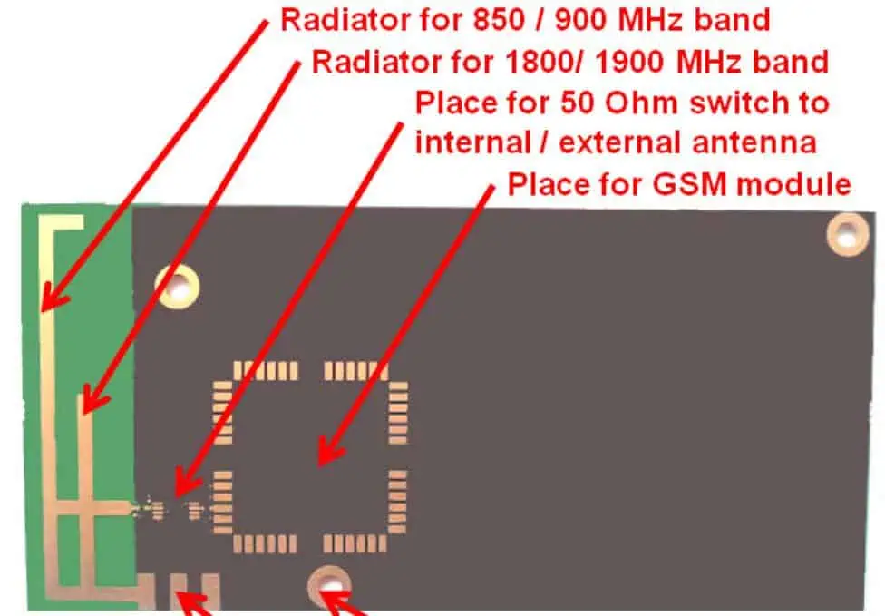
Antenna positioning
PCB antennas have various operation modes. However, there are some particular positions you need to place them based on the antenna’s radiation level. For instance, you can place them in the corner of the circuit board or along the short side of the board. There are different designs for antennas that are ideal for various positions. Therefore, PCB designers can choose the antenna based on their layout and application.
Closeness to other components
During the design phase of a PCB antenna, you must ensure the embedded antenna isn’t close to other components on the circuits. The height and width of the component determines the distance between other components and the antenna. Components such as LCD s and batteries can have switching speeds. This can help with more signal interference during the functionality of the device.
Keep-out area
Designer need to be sure the components aren’t positioned in the near field around the antenna. Otherwise, this may cause signal interference, which impacts the functioning of the circuit. Furthermore, ensure the area around the antenna isn’t in contact with metallic objects.
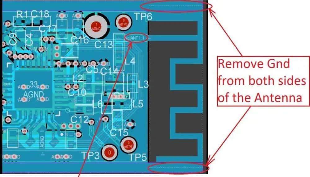
Ground planes
The ground plane’s size on a circuit board is a crucial factor you need to consider. This is because wires used for creating communication between different batteries and devices may change if not properly designed. Therefore, designers need to ensure proper sizing of the ground planes. If properly done, batteries and cables linked to the device have less impact on the antenna.
Design the transmission line
In PCB antennas, the transmission line is an RF trace which transmits RF energy. Designers need to design the transmission line at 50Ω as this may reflect signal to the reception. This may result in a degraded signal-to-noise ratio.
Fundamentals of PCB Antenna Design
Antennas serve two basic functions. These include the emission of electromagnetic waves when there is a current and a voltage. Also, they get electromagnetic waves and transform them into a current and a voltage. The interconnect will have to transfer a signal into the antenna or receive a signal from it.
Furthermore, PCB antennas are usually designed to pick up a magnetic or electric field. Magnetic antennas integrate a loop of wire. The receiver/transmitter element in this system functions in a similar way with a load that completes a circuit board that features the loop antenna.
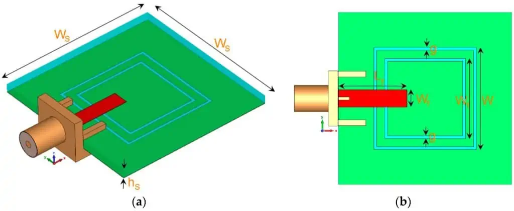
The physical design of an antenna
A designer aims to define an antenna’s geometry so that they can meet some operating goals such as feedline matching, high radiation efficiency, sufficient bandwidth, directionality, and low loss along front end and feedline. The positioning of an antenna and its physical design will determine these operating properties.
PCB antennas make use of wave resonances present within the structure of the antenna to form a string current oscillation. With this, designers would be able to achieve magnetic and electric field generation around the antenna. Therefore, one of the drawbacks of antenna design is determining the resonances in the structure of the antenna.
After the designer determines the electromagnetic field around the antenna, he determines the radiation efficiency and radiation pattern with software.
The input impedance is another physical aspect to consider for an antenna. You need to know that PCB antennas can posses a reactive component on the input impedance. This will determine how a matching network should be designed for the antenna.
Feedline Design
It is important to design antenna feedlines to get a signal from conductive feedline. This has to be a part of a transmission line designed for a particular impedance that tries to match the impedance of an antenna. Transmission lines are resistive in their characteristic impedance. However, PCB antennas can feature a reactive component.
Therefore, feedline should be designed in a way reduction occurs in the return loss along the feedline. If the feedline isn’t properly implemented, it can limit the bandwidth. Therefore, it is crucial designers choose the right matching method for their exact antenna.
How to Achieve a Better Performance When Designing a PCB Antenna
There are different ways you can improve the performance of your PCB antenna. Below are some ways:
- Integrate matching networks when during antenna tuning. This helps in compensating for factors that may impact the performance of the antenna.
- Avoid designing an external casing for an antenna as this may interfere with the signal.
- Ensure the ground plane you selected is appropriate. If not, this will result in crosstalk between the signals.
- Do not place the PCB antenna too close to plastic surfaces. Doing this can have a negative impact on the performance of the antenna. Furthermore, plastic usually features a higher Dk than air. This impacts transmitted signals and can cause losses.
- Consider the signal bandwidth when designing a PCB antenna.
Conclusion
Antennas serve two basic functions. These include the emission of electromagnetic waves when there is a current and a voltage. Also, they get electromagnetic waves and transform them into a current and a voltage. Learning how to design PCB antenna requires following certain guidelines to achieve the best result.