PCB trace antenna design is very complex. The target bandwidth frequencies determine this antenna size. PCB trace antennas offer some benefits which include low cost and great performance. This antenna is usually embedded in a circuit board.
The size of this PCB antenna is very small for frequencies above 900 MHz. Therefore, when used for low frequencies, it is crucial to increase the size of this antenna to keep the integrity of the signal to resonance frequency.

What is a PCB Trace Antenna?
A PCB trace antenna functions as a wireless communication method. It comprises trace directly drawn on a printed circuit board. Also, during PCB manufacturing, it is important to laminate the trace on the PCB surface. However, PCB traces usually cover several layers, particularly in multi-layer circuit boards.
A PCB trace antenna is difficult to design, tune, and integrate. The target bandwidth frequencies determine the antenna’s size. PCB Trace antennas have their own benefits. These low cost antennas perform well. Also, they are usually embedded in the circuit board during manufacturing. However, the size of this antenna is very small for frequencies that are above 900 MHz. Designers will need to increase the size of the antenna to ensure the signal integrity has resonance frequency.
PCB Trace antennas have some drawbacks which don’t make them a suitable choice in some cases. The design process of these antennas is very complex especially at very low frequencies. Also, PCB Trace antennas occupy more space which increases the general cost of design. Nearby components impact the performance of these antennas as they are prone to environmental disruptions.
These antennas are usually embedded into the circuit board. Therefore, the circuit board will need a redesign if there is any change in the antenna design. A PCB trace antenna is a crucial component of a wireless system. Unfortunately, some designers see them as an afterthought in their design. Planning for a PCB trace antenna design will help in achieving product performance.
More so, there will be no need for reproductions and delays in the later phases.
Considerations for PCB Trace Antenna Design

When designing a PCB trace antenna, there are certain factors which must be considered. The PCB trace antenna design process is a complex one and as such, there is a need to pay attention to some crucial factors. When good decisions are made about these factors, you will achieve a successful PCB trace antenna design.
PCB construction
The construction of the circuit board is an ideal consideration when designing a PCb trace antenna. The resonant frequency of a PCB is determined by the length of the copper PCB trace. The trace becomes shorter when the frequency is higher. Furthermore, every antenna requires an area around the trace without copper traces. Wide traces enable a wide bandwidth. The material of the substrate, its thickness, and dielectric constant will determine the electrical signal performance of the antenna.
Add matching components
The RF link budget and range performance can be minimized by mismatched antennas. In order to prevent any mismatch losses, it is advisable to position a pi-network at the feed point of the antenna.
Asides from placing matching components, make sure the source impedance and the antenna match. You can as well maintain a return loss ≤ -10dB.
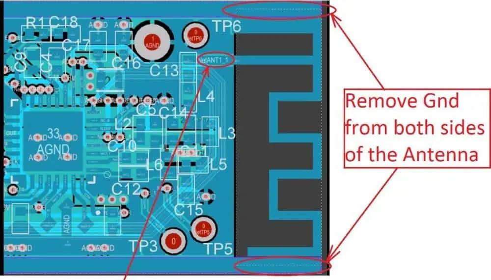
Ground plane
Ground planes are very crucial in PCB antennas. The impedance and performance of the antenna will depend greatly on the shape and size of the ground plane. Therefore, ensure the ground plane has vias along the keep-out area of the antenna.
Antenna’s environment
The environment of the PCB trace antenna is a crucial consideration during design. Metal components can have an effect on the radiation tuning and pattern. Therefore, designers should keep the PCB trace antenna far from metallic enclosures or metal objects.
2D structure
When PCB trace antennas are embedded in the circuit board, their 2D structures feature the same plane as a ground plane. Therefore, this restricts the antenna’s volume. If there is a limited surface area for the antenna, PCB trace antenna would have less performance due to the lack of 3rd dimension.
Pros and Cons of a PCB Trace Antenna
PCB trace antennas have their benefits and limitations. Some people have argued that these antennas are usually difficult to create, tune, and apply. Furthermore, the size of these antennas depends on the bandwidth frequencies. Here are some benefits of a PCB trace antenna.
- The cost of producing these antennas is very low. This is because the trace must be integrated in your PCB manufacturing process.
- Furthermore, this antenna can give room to a wide bandwidth when it is maximally tuned.
- The structure of a PCB trace antenna is very simple. The structure profile is because the antenna is placed on the surface.
- It offers more strength capacities and improved network reliability.
- It is very easy to insert this antenna in a circuit board during production.
Cons
- This antenna is difficult to create, especially at low frequencies.
- Also, a PCB trace antenna is vulnerable to modifications performed in a PCB-layout modifications.
- This antenna requires enough space at low frequencies.
- The cost of PCB trace antenna design increases due to the need for more board space.
- A PCB trace antenna design is vulnerable to environmental and human factors.
Challenges Associated with the Integration of PCB Trace Antenna

The integration of a PCB trace antenna in devices can be a challenge, especially in compact devices. Therefore, it is crucial to understand some risks associated with this trace antenna.
These antennas are known to be very complex in terms of performance, particularly when there is a need for multiple frequency bands. Since wireless performance has become a major factor of SMART devices function, you should look into the implications of choosing a trace antenna over a chip.
Design Flexibility
PCB trace antenna designed is known for inflexibility. The operating environment determines the performance of these antennas. Therefore, designers need to consider a number of factors when integrating a wireless antenna. However, a PCB trace antenna reduces the flexibility designers have to integrate wireless antenna.
Furthermore, trace antennas are 2D in structure and as such, they occupy more space than a chip antenna. Any attempt to minimize a trace antenna’s footprint will affect its performance. Chip antennas perform within a small footprint.
In addition, trace antenna’s performance can be influenced by changes between the planned design and the first manufactured designs. Technical catastrophe is associated with the integration of trace antenna. This is because this antenna has sensitivity to even the slightest changes.
Once PCB trace antennas are produced, it is impossible to tweak them since they are embedded on a circuit board. Dysfunctional PCBs with a trace antenna can’t be repaired or fixed since it is less easy to manipulate the tuning of this kind of antenna. This is because of the PCB materials tolerances’ composition.
Operating Environments
Although PCB trace antennas are affordable to manufacture, they cannot offer high levels of performance in some operating environments. External operating environments and internal operating environments can possibly cause some RF issues. Instability in the operating environment will result in more drastic issues for a PCB trace antenna.
A PCB trace antenna poses some risks especially when the distance or quality of a radio frequency signal is crucial. Therefore, this antenna isn’t an ideal option in such cases.
Detuning Effects
PCB trace antennas are prone to detuning effects. The host printed circuit board will integrate low cost FR4 materials in most typical devices. But, these materials feature high levels of loss and can’t be tightly controlled as regards their ER. The dielectric constant (dK) will as well change over frequency. This occurrence will affect final performance in manufacture.
Moreso, human operators and components can detune an antenna to a certain degree. This shift in frequency can result in degraded functioning or make the device malfunction. The performance of trace antennas is limited as a result of this. For instance, handheld devices are vulnerable to degraded performance, particularly when integrating a trace antenna.
Noise
PCB trace antennas have more susceptibility to noise than chip antennas since they are being used as part of the host PCB. One of the causes of the issues experienced when integrating a PCB antenna is interferences. This makes several devices to malfunction at the first attempt at design. A chip antenna may perform much better where there is a high noise. This is possible due to a chip antenna’s 3D structure. The 3D structure reduces the noise effects of components that are close. The antenna chip is. tuned to meet a device’s requirements.
What is the Difference between a Chip Antenna and a PCB Trace Antenna?
One of the factors that affect the performance of an antenna is the PCB layout. Therefore, it is important for designers to tune the antenna to get the maximum system performance. Proper electrical resistance matching helps in achieving all-out frequency transmission.
The PCB trace antenna design is embedded in the board design, this makes it difficult to perform tuning and achieve maximum performance. Asides from that, minimal dielectric PCB permittivity makes the antenna susceptible to tolerance variants and design alterations. In situations like this, the circuit board needs to be re-spinned to achieve excellent antenna performance.
Key Parameters of Antenna Performance
Return loss
The return loss reveals how the antenna matches to a transmission line with an impedance of 50Ω. 50Ω is the impedance value of the transmission line; however, it is possible to have other values. A commercial antenna’s resistance is 50Ω. Therefore, it is advisable to use this value.
Also, the return loss shows the amount of incident power the antenna reflects as a result of the mismatch. A suitable antenna will discharge all the power with no reflections.
Bandwidth
Bandwidth describes the antenna’s frequency response. It reveals the relationship between the antenna and the 50Ω transmission line in the whole frequency band integrated.
Radiation pattern
A PCB antenna’s radiation pattern is the direction of radiation. It reveals the direction at which the radiation is higher and the direction at which the radiation is lower. Therefore, this helps in identifying the antenna’s direction in the application.
Non-directional antennas are capable of transmitting equally in all directions. However, the majority of antennas can’t achieve this performance.
Antenna gain
This is a parameter that offers the necessary information for the comparison of the radiation of the direction with an isotropic antenna. dBi represents the antenna gain unit. This refers to radiated field strength.
Radiation efficiency
Radiation efficiency reveals that the antenna consumes part of the non-reflective power as heat. The conductor loss in the copper wire and the dielectric loss in the substrate is responsible for the heat produced. The whole non-reflective power is discharged when radiation efficiency amounts to 100 percent. The heat loss is very low for small board form factors.
Design Guide for PCB Trace Antenna
PCB trace antennas offer improved performance, while step providing repeatability and low cost. These antennas are very easy to tune.
Sizing the Feedline
The feed line is the trace which links the antenna to the matching circuitry’s output. You need to design this to be 50 Ohms. The trace width determines the impedance.
Impedance Matching
Impedance matching when designing a PCB trace antenna is a big rule engineers must adhere to it. There are chips that transmit a signal and there is a need to transform electrical signal into a wireless one. There are characteristics that define the impedance of the antenna and chip. If there is equal impedance, much power is being put on the wireless signal. If there is no perfect impedance matching, there will be some loss of power.
Conclusion
PCB trace antenna design is one of the most common problems experienced in circuit boards and electronics. It has become a challenge for designers to keep the board size small without having an impact on the performance of the antenna. Therefore, it is crucial to consider PCB trace antenna design early in the development stages to prevent delays as a result of changes in design.