When choosing the correct antenna for your embedded designs, understanding the differences between chip and PCB antennas is important. Your electronic equipment requires the antenna to link via radio frequency (RF). Examples of Radio Frequency devices commonly found in electronic manufacturing include walkie-talkies, Bluetooth-enabled gadgets & satellite communication devices. Antennas play a vital role in the performance of RF devices and can have a significant impact on their overall effectiveness. In modern RF applications, the primary needs for antennas are super performance, reduced size & low cost.
When comparing chip antennas versus PCB antennas, it’s essential to consider a PCB trace antenna if cost reduction is a priority. Conversely, Ceramic Chip antennas are more efficient in miniaturization and overall performance. This blog delves into the chip antenna versus PCB antenna debate, exploring the advantages and disadvantages of each and providing guidance on the design needs you should understand when selecting the appropriate antenna for your project.
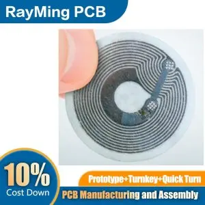
Ceramic Chip Antenna

While comparing PCB antenna Vs. Chip antenna, it’s important to note that Ceramic Chip Antenna has a minor spatial requirement and can be easily integrated into printed circuit boards for generating radiofrequency signals. However, they have minimal radio frequency ranges and are better suited for small devices such as Wi-Fi routers & smartphones. In essence, Chip antennas function like other antennas by transmitting and receiving radio frequencies. PCB antenna, in comparison, are more significant than their smaller counterparts. This compact size makes them easier to mount inside electronic devices. Additionally, Chip antennas are a cost-effective alternative that does not compromise product quality.

PCB Trace Antenna
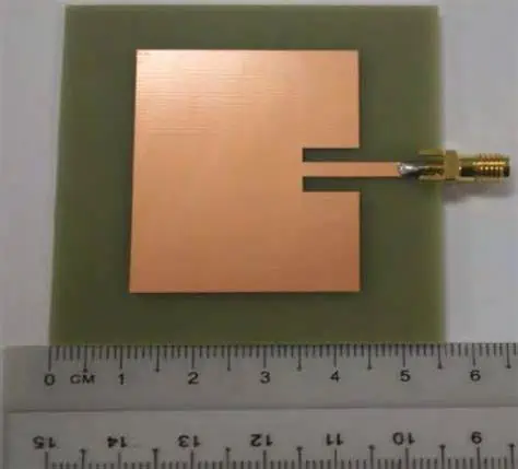
It is important to note that the type of antenna and spatial needs determine the type of trace used in a PCB trace antenna. The paths can take different shapes, such as inverted F-shape, straight, meandered, curved, and circular, among others.
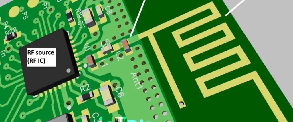
In general, a Printed circuit board trace antenna is used for wireless communication purposes. During the PCB manufacturing process, the trace is typically laminated onto the board’s surface. However, in some cases, PCB traces may cover multiple layers, particularly in multi-layered printed circuit boards.
Learn More about:
- NFC Antenna
- LoRa antenna
- 2.4 GHz Patch Antenna
- 2.4 GHz PCB Antenna
- BLE PCB Antenna
- Dipole Antenna
- Inverted-F Antenna
- Monopole antenna
- PCB Loop Antenna
Ceramic Chip Antenna Vs. PCB Trace Antenna

Pros of Ceramic Chip Antenna
When comparing Chip antennas to PCB antennas, it is clear that using a monolithic ceramic antenna has many advantages. First, it eliminates the need for expensive prototype production & simulation software due to its network-tuning capability and lack of physical properties. Additionally, monolithic ceramic antennae offer another advantage such as:
· Ceramic Chip antennas come as discrete parts.
They offer easy availability of numerous configurations and small sizes for various designs.
The proximity to other parts, which is not as close as in Printed circuit board Trace antennas, does not cause any adverse effects.
· Chip antennas are less affected by environmental & human factors than Trace antennas.
They provide flexible tuning & testing options.
Design modifications are easy to introduce with Chip antennas.
Cons of Ceramic Chip Antenna
Ceramic antennas have some drawbacks, too. Here are some cons of using Ceramic PCBs
- Ceramic antennas may have higher initial costs & logistics costs compared to printed circuit board Trace antennas.
- Implementing Ceramic antennas requires some RF knowledge for optimal performance.
- Ceramic antennas may have lower performance compared to Trace antennas.
Pros of PCB Trace Antenna
People who support using Chip antennas over PCB antennas say that making and adjusting a printed circuit board trace antenna can be challenging, especially for small devices. The size of the trace antenna depends on the frequency it needs to operate at. However, some advantages are using a PCB trace antenna.
- PCB trace antennas have low production costs as they can be integrate able into the board production process.
- When maximally tuned, they can accommodate a broad range of bandwidth.
- The structure of a PCB trace antenna is simple and has a thin profile since it is placed on the board surface.
- It offers better strength & network reliability compared to other types of antennas.
- It can be easily integrate able into the printed circuit board during production.
Cons of PCB Trace Antenna
The following are the disadvantages of the Trace antenna:
- Creating a trace antenna is difficult, especially at lower frequencies.
- Printed circuit board layout modifications can affect the performance of a trace antenna, requiring frequent tuning.
- Trace antennas require a significant amount of space, particularly at lower frequencies.
- Increasing the board size to accommodate the antenna leads to higher design costs.
- Trace antennas are vulnerable to environmental and human factors.
Chip Antenna Vs. PCB Trace Antenna – Antenna Design Tips
Antennas are essential parts of wireless systems, yet many designers overlook their importance. If you plan your antenna design early in the manufacturing process, you can maximize product performance and avoid delays and redoing work later on. Here are some essential tips to help you prepare for an integrated antenna design.
· Materials
When designing your antenna, ensure that the material you use to create it, whether a board, stamped metal, or plastic, has consistent dielectric properties. It’s important to note that low-cost dielectric FR4 circuit board materials can vary significantly between suppliers. To avoid issues, specify the board materials you want to use.
· Physics Suggestions
To ensure your electronic equipment has an excellent performance range, you need to have a sound antenna system in place. It’s also important to leave enough space for the antenna system. That’s why it’s necessary to be available in the early stages of the device’s production cycle. It will allow you to discuss and agree on the choices and avoid compromises.
· Product Location
The placement of the antenna on the edges of your device can make it sensitive to surrounding environmental factors. Thus, it’s necessary to understand how you intend to use the device and where you place it. For example, if it’s a handheld device, you should ensure that the antenna is not coverable by the user’s hands when held naturally. Similarly, for the wall-mounted equipment, you should consider whether the users will attach them to metallic surfaces that can affect the device’s performance. Considering these factors during the design phase, you can ensure optimal performance and avoid potential issues.
· Casings & Coatings
To achieve high antenna performance, avoid covering your antenna with a metallic coating. Also, collaborate with your mechanical & ID colleagues to ensure that the area surrounding the antenna is clear of any potentially disruptive materials.
· Internal Structures
The position of any internal metallic components of an antenna can also impact the product’s performance. For example, in wearable devices, the battery is a significant element of the overall assembly, so you must carefully consider its location & function when designing the antenna.
· Antenna Weight
An integrated antenna refers to the physical component, such as the Printed circuit board-carved part. However, in many cases, it forms only one part of the antenna system. The half comprises the main system ground. As the primary circuit board ground, it is essential to ensure enough weight to allow an antenna to vibrate correctly.
· Circuit Sensitivities EMI/RFI
Wireless systems have receivers and transmitters. The transmitter causes interference with nearby circuits, affecting the receiver’s performance. To avoid this, it is essential to position the antenna in a way that minimizes interference with sensitive circuitry and maximizes the product’s wireless performance.
Chip Antenna Vs. PCB Trace Antenna: Antenna Frequency

Tuning the circuit board layout is vital to achieving optimal antenna performance. It’s important to note that proper impedance matching ensures maximum electromagnetic transmission in a desired band.
When tracing antennas, tuning and achieving maximum performance can be difficult due to the antenna design being tied to the overall board design. Additionally, minimal dielectric circuit board permittivity makes the antenna highly susceptible to design modifications & tolerance variations. As a result, re-spinning the PCB may be necessary to achieve optimal antenna performance.
The Π-type method is a popular choice among engineers regarding Ceramic antennas due to its flexibility in bandwidth tuning. This method allows for adjusting matching aspects to address any in-built detuning.
To design a matching network for your antenna, it is recommended to use a VNA to analyze your printed circuit board test circuit. The VNA can also help you determine the antenna load impedance, S-parameters, VSWR band, and on-printed circuit board Ceramic efficiency.
At WellPCB, we offer optimization services for Ceramic antennas. Our team of RF experts uses advanced technology to adjust the matching network to your desired resistance for optimal performance. Matching improves antenna efficiency within the chosen bandwidth in your product’s operating environment. We also assess design layouts to ensure proper utilization of PCB space.
· Design considerations
When using these antennas, it is essential to know the following design considerations:
· Antenna types
Knowing the various antenna types available and their functionality in different scenarios can be crucial in selecting an optimal antenna in size, efficiency, and cost. Therefore, it is essential to familiarize oneself with these standard antennas.
· Circuit board construction
When constructing a circuit board, it’s crucial to ensure that the antennas have adequate free space surrounding them, without any copper traces/ground fill. For chip antennas, it’s also essential to follow a guideline provided in the datasheet. Other factors that can impact the performance of the antenna include the substrate substance used, as well as its thickness and dielectric constant. Therefore, it’s essential to take all of these aspects into consideration for optimal antenna performance.
· Ground plane
The performance of trace antennas & chip antennas is influenced by the plane they are placed on. The size & shape of the ground plane can have a significant impact on antenna performance. It’s advisable to consider the minimum frequency of the operating range to determine the optimal size & shape of the ground plane. By doing so, the ground plane can be designed to enhance the antenna’s performance.
· Matching network
If an antenna is poorly matched, it can lead to a decline in the network’s overall performance. It can result in increased energy consumption, reduced range, and communication damage. A matching network can be utilized between the antenna and the transmitter to prevent this. This device improves power transfer by ensuring that the impedance is matched correctly.
· Surrounding environment
Designers should know the environment surrounding the antenna placement. It’s advisable to avoid metallic elements near the antenna to ensure optimal tuning & radiation pattern. Additionally, the use of metallic enclosures should be avoided as it can affect the effectiveness of the antenna.
· Never do an existing design
Designers are not recommended to replicate a previous antenna design from one application to another. It is because the tuning & radiation patterns are heavily influenced by the surrounding elements, which can vary significantly between applications. A design suitable for one application may not function effectively for another. Therefore, the tuning & radiation patterns must be readjusted to account for the different surrounding components. In addition, the antenna length and base plane size may also need to be reconfigured. Consequently, utilizing the existing design for new applications could potentially impair performance.
Final Thoughts
When comparing Chip antennas to PCB antennas, it can be noted that they are less susceptible to detuning from environmental factors and humans. In multi-radio equipment, using two Chip antennas provides excellent antenna-to-antenna isolation, surpassing the performance of PCB antennas. Therefore, selecting the appropriate antenna type & implementing it can result in superior performance compared to PCB antennas.
It is crucial to conduct OTA (Over the Air) measurements to evaluate the antenna’s performance in the final product’s practical setting. In the case of PCB antennas, failures during assessment can be difficult and expensive to rectify, often necessitating several board iterations. On the other hand, Chip antennas are separate components, making it much easier and quicker to improve their performance if needed. It is essential to keep this in mind while testing the antenna performance. By modifying only the antenna component, it is possible to adjust the tuning and test the system’s performance. We trust that the comparison guide between Chip antennas and PCB antennas will assist you in selecting the appropriate antenna for the integrated designs.
With the world increasingly adopting wireless technology, designing antennas has become a crucial challenge. It can be difficult for designers to maintain a small board size without compromising the antenna’s effectiveness. Antenna design should be in the early stages of development to prevent any delays because of design changes at later stages.