
RAYPCB · Near-field coupling workshop
NFC antenna: design the coil around the tap
Separate reader and tag designs, account for metal and ferrite, and calculate a first resonance allowance from measured coil data before final matching.
Preliminary layouts and open RF questions are welcome.
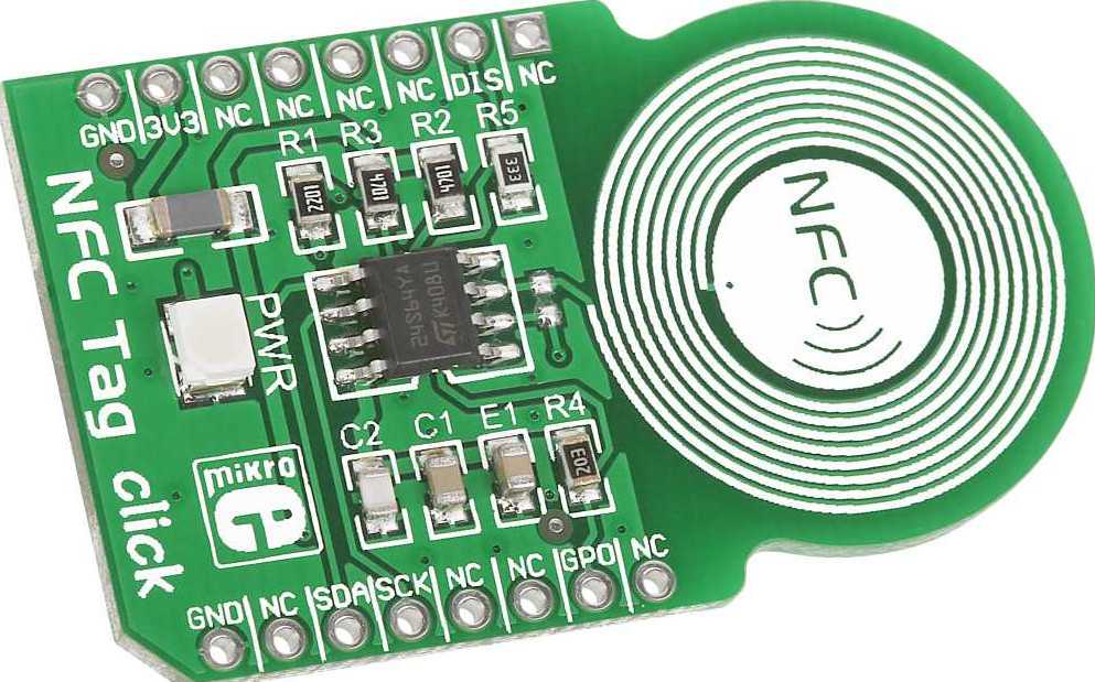
What is an NFC antenna?
An NFC antenna is normally a conductive loop used for magnetic coupling at 13.56 MHz. In a reader, the RF circuit drives a field and detects the response of another device. In a passive tag, the loop and IC form a loaded resonant system that obtains energy and communicates through that coupling. Both use a coil, but their matching, loading and verification tasks are different. The right design starts with the selected IC and the intended tap interaction.
Think about the user's action before optimizing turns. Where will the phone or tag touch the product? What is behind the coil? Is the enclosure plastic, coated, metallic or flexible? Which reader and tag sizes need to work together? A technically neat loop can fail the product if its useful coupling region lies behind a metal bracket or if the expected tap direction was never tested.
This guide covers coil design and integration. For fabrication requirements and an NFC board enquiry, continue to NFC antenna PCB manufacturing. For radiating antenna families at other frequencies, use the antenna PCB overview; a 2.4 GHz wavelength calculator is not an NFC coil-design method.
Reader and tag are two different circuits
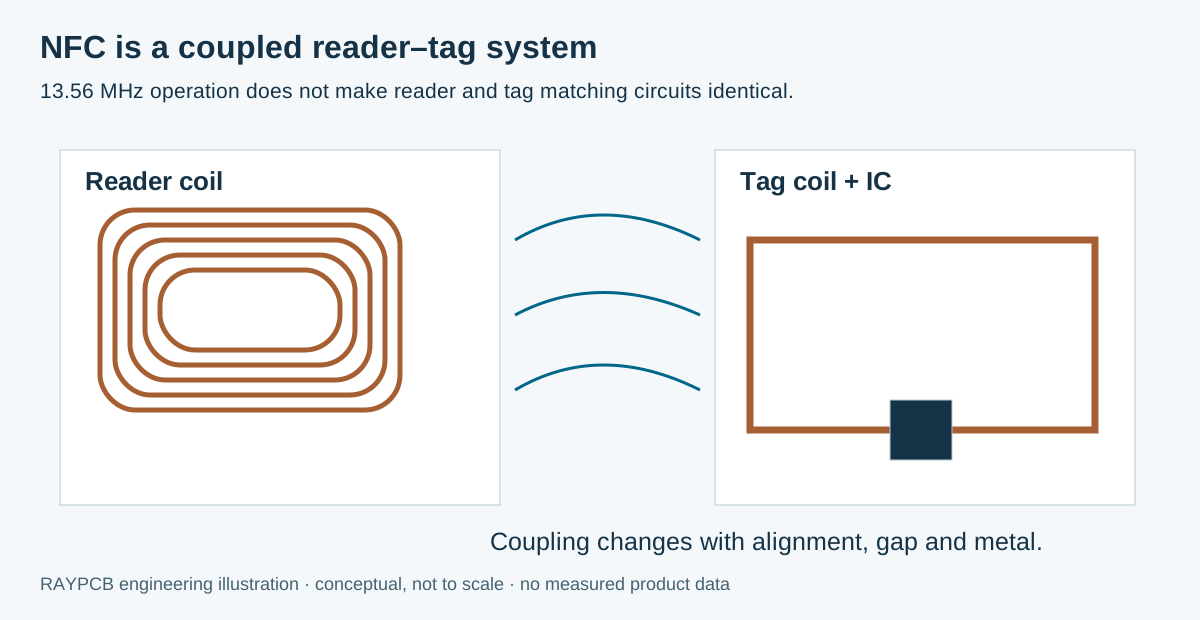
| Design task | Reader antenna | Passive tag antenna |
|---|---|---|
| Excitation | Powered RF driver and matching network | Coupled energy from a reader field |
| Main circuit questions | Driver loading, filtering, damping and modulation | IC input, tuning, available energy and load modulation |
| Useful measurements | Coil impedance and complete driven-system behavior | Loaded resonance, communication and energy behavior |
| System boundary | Reader, matching network, coil and intended targets | Tag coil, IC, host object and intended readers |
Select the IC before committing to a generic matching schematic. A reader with differential outputs and an EMC filter is not represented by a single ideal capacitor across a coil. A tag IC also presents an effective input that may depend on its operating condition. Use the manufacturer-defined equivalent circuit and test procedure for the actual device, rather than combining values from several unrelated application notes.
NXP's NFC antenna design training connects antenna matching with the metal environment, debugging and qualification. Use that workflow to organize the design review, then obtain the matching guidance for your selected reader or tag IC. A component network from a different device is not an interchangeable design.
Turn the physical tap area into a coil drawing
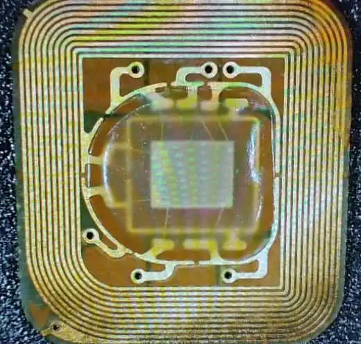
Start with the available loop outline, intended coupling face, mounting tolerances and nearby materials. Then choose turns, conductor width, spacing and layer transitions within that envelope. More turns can increase inductance, but also alter resistance, parasitic capacitance and self-resonance. A larger loop does not automatically couple best to every target size or every tap distance. The design problem is a coupled system, not a contest to maximize one isolated value.
Specify finished copper rather than only starting foil when resistance matters. Keep the transition between coil terminals and the matching circuit deliberate. Long connecting traces add electrical behavior and may couple to other circuitry. If a crossover uses a second layer or vias, include that geometry in the model and drawing. Do not add an unreviewed ground plane under the loop simply because the rest of the board benefits from one.
The loop's location relative to the product is part of its definition. An adhesive-backed flex coil can place the coupling region close to an enclosure surface, while a rigid coil may offer more controlled attachment to the electronics. Review the flex tail, connector and bend zone independently from the loop. The flexible PCB manufacturing guide covers the construction choices needed when the coil becomes a flexible circuit.
Calculate an initial resonance allowance
This tool uses measured inductance and effective capacitance to examine an ideal lumped parallel resonance. It calculates total capacitance at a chosen target frequency, subtracts the entered IC and stray capacitance, and estimates unloaded coil Q from AC resistance. It also shows independent tolerance corners for inductance and total effective capacitance. The outputs help organize a tuning discussion; they are not a complete reader matching network or a reading-distance prediction.
RAYPCB ENGINEERING
Antenna BandsNFC Coil Resonance Planner
Loading NFC Coil Resonance Planner…
At the illustrative 13.56 MHz target, a 1.5 µH inductance gives an ideal total capacitance of about 91.84 pF. If the entered effective IC and stray capacitance is 25 pF, the remaining ideal allowance is about 66.84 pF. These values are a teaching example. The actual target and equivalent circuit must come from the selected device, and the assembled network must be measured after component and environmental effects are included.
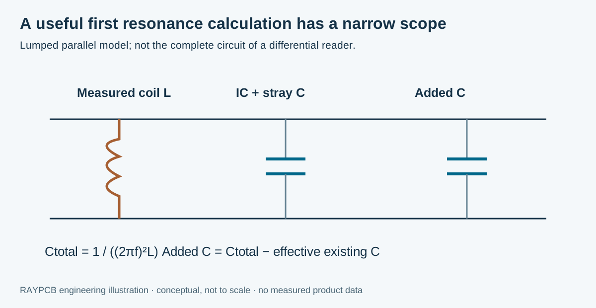
A negative additional-capacitance result has a useful meaning: the existing effective capacitance is already greater than the ideal total at the entered inductance and target frequency. The tool does not hide this by returning zero. Revisit the inductance, target, equivalent circuit and measurement basis. Adding a positive parallel capacitor cannot correct that particular idealized condition.
Use AC resistance at the target frequency for the Q calculation. A multimeter's DC resistance does not include every high-frequency loss. Unloaded coil Q is also different from the loaded network Q once the IC, damping and coupling are included. A very high isolated Q is not automatically desirable if the communication bandwidth or modulation response becomes unsuitable.
Treat ferrite, metal and adhesive as part of the antenna
Metal near a loop can support induced currents that change the field and the electrical behavior. A ferrite layer may help a design operate near metal, but its grade, thickness, dimensions and placement matter. It can change both inductance and loss. The proper comparison is between complete installed structures, not between a bare coil measurement and an unspecified ferrite sheet.
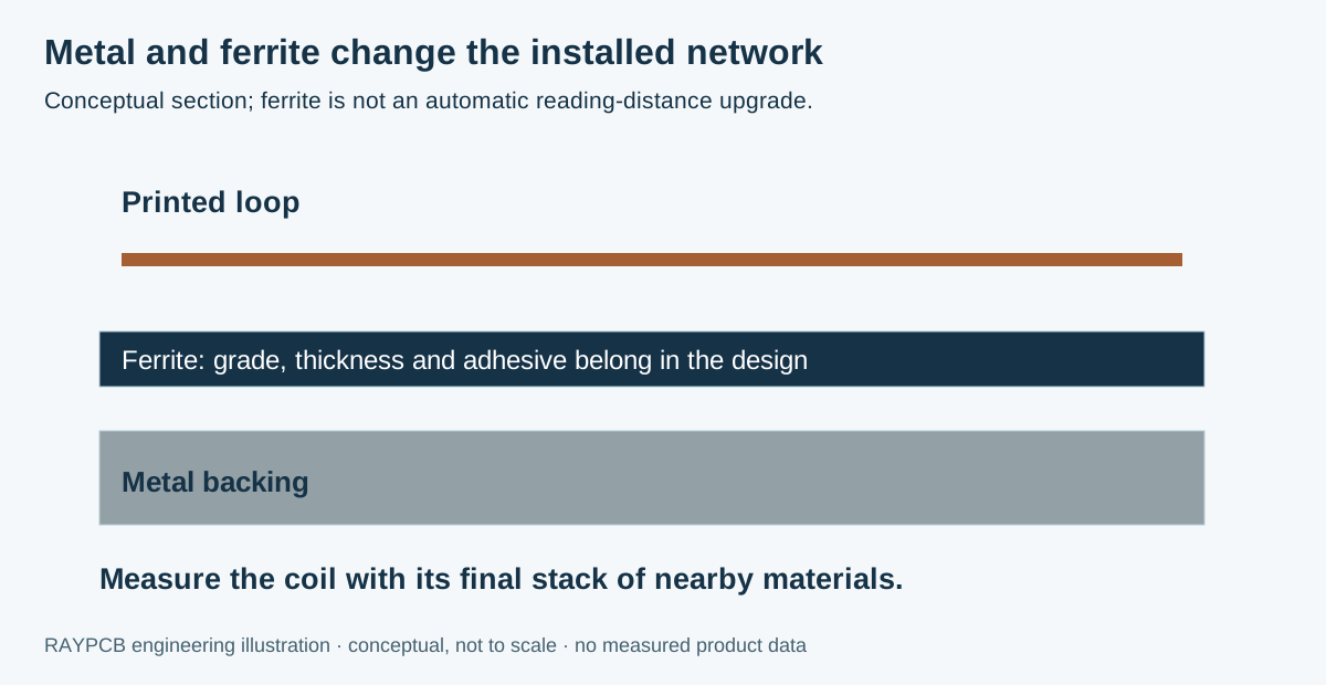
Record the full stack: enclosure surface, adhesive, coil, insulation, ferrite, spacing and metal backing. Include tolerances and the expected temperature or mechanical changes. A label or decorative finish can be relevant if it contains conductive material. Test actual production-intent materials instead of substituting convenient samples that only look similar.
For a wearable or curved product, retain the formed position during measurement. For an industrial reader, include the mounting bracket and cable route. For a tag attached to a container, evaluate the intended contents and fill conditions where they influence coupling. A drawing that identifies only the PCB cannot communicate these external conditions to the engineering team.
Use the IC-specific method for the final circuit
The NXP NTAG I²C plus documentation and antenna-tool resources provide a device-specific starting point for a connected tag. For a reader, obtain its own IC documentation: matching can include damping, filters and component-rating decisions that a resonance equation does not address. Use the chip vendor's current tool or reference method when synthesizing that network, then keep its input measurements and revision with your design record.
Pay attention to the schematic-to-layout transition. A capacitor connected through a long route and an unexpected ground return does not behave like the ideal symbol in a schematic. Identify the measurement plane, component packages, conductor paths and test access. Keep approved substitutions explicit; a component with the same nominal capacitance may have different tolerances or high-frequency characteristics.
Bring up the network in controlled steps. First establish whether the standalone coil measurement is credible. Then assemble the intended matching network and IC configuration. Evaluate the driven reader or loaded tag using the applicable vendor procedure. Finally repeat the relevant tests in the housing and against the required counterpart devices. Changing several network values and the mechanical stack at once makes a poor result difficult to explain.
Verify a tap volume, not one successful tap
A useful NFC verification plan covers position, orientation, gap and representative counterpart devices. Mark the intended interaction zone on the product. Test centered and off-center placements, realistic approach angles and repeatability across samples. Record communication completion, retries or failures at a defined application step. One successful transaction on a bench proves much less than a repeatable interaction across the intended user envelope.
Separate electrical and application observations. Coil impedance helps explain the RF network. Protocol and interoperability tests address communication. Power-related tests matter for energy-harvesting or passive operation. Authentication and payment security depend on the selected system and implementation; an antenna design alone cannot make those claims.
| Verification record | Include | Decision supported |
|---|---|---|
| Coil measurement | Frequency, fixture, installed stack and instrument settings | Whether the electrical starting point is reproducible |
| Network revision | IC settings, matching population and component packages | Which circuit produced the observed result |
| Coupling map | Counterpart, position, angle, gap and sample count | Where the intended interaction works reliably |
| Product release | Housing, adhesive, ferrite and mechanical tolerances | Whether a manufacturing change needs revalidation |
NFC applications range from product pairing to configuration, identification and access interaction. Define the actual transaction and its completion criteria instead of using a vague requirement such as good range. If the device is part of a larger connected product, the IoT PCB integration page helps connect power, radio, security and manufacturing responsibilities.
Prepare a coil or assembled-board enquiry
For a bare coil PCB, send the outline, conductor geometry, copper requirements, layer connections, finish and terminal details. For a flex version, include substrate, coverlay, adhesive and any formed position or stiffener. For an assembled reader or tag board, also provide the BOM, placement data, IC programming requirements and matching population. State which tests are required and who supplies the counterpart devices or fixtures.
Open optional hardware budget and RFQ brief
RAYPCB ENGINEERING
Antenna BandsAntenna Hardware Budget and RFQ Brief
Loading Antenna Hardware Budget and RFQ Brief…
The budget brief can separate per-unit hardware, one-time setup and batch verification allowances. It accepts your dated cost evidence instead of applying a generic RF multiplier. Include ferrite, purchased antenna parts and assembly only when those items are expressly covered. Leave costs blank when you need a technical discussion first. A realistic quotation needs the complete scope; a low bare-PCB price says little about the cost of a validated NFC product.
For the broader board service, review PCB manufacturing. When requesting review, identify whether the open issue is coil fabrication, IC matching, metal interaction or complete-product testing. That single distinction helps route the enquiry to the right engineering discussion without forcing you to finish every calculation first.
Practical NFC antenna questions
Should every NFC coil resonate exactly at 13.56 MHz?
The communication carrier is 13.56 MHz, but the appropriate standalone or loaded tuning target depends on the circuit and vendor method. Use the selected IC's guidance and clearly state what was measured. Do not assume the optimum isolated-coil target is identical for all reader and tag networks.
Can I calculate the number of turns from reading distance?
Not reliably with one universal equation. Reading behavior depends on the paired antennas, orientation, loading, IC operation, environment and protocol. Start with the physical and electrical requirements, then use modeling and measurements to evaluate the intended coupling volume.
Does ferrite eliminate the need for tuning near metal?
No. Ferrite changes the installed structure and may be part of a successful solution, but it does not remove material or geometry dependence. Measure and validate the coil with the actual ferrite, adhesive, metal and enclosure arrangement.
Is the online result enough to release a matching BOM?
No. The worksheet is a transparent resonance screen. It does not synthesize a differential reader network, establish component voltage ratings or verify communication. Use the device-specific method, then retain measured evidence for the final assembled design.
Review an NFC coil and installation
Send the radio and antenna reference, board revision, intended bands, enclosure information and quantity. Include the measurements you have and the question you need to resolve.
Tool use is optional. Attach any downloaded brief manually; Contact does not automatically receive worksheet inputs. References reviewed September 2026. Illustrations are explanatory, and photographs are not process qualification records.

