NFC or Near Field Communication is a short-range wireless connectivity technology used in applications like contactless payments, proximity identification, automotive infotainment and more. NFC enabled devices contain specialized NFC antenna PCBs to transmit and receive NFC signals on the 13.56MHz frequency.
In this comprehensive guide, we will explore what NFC antenna PCBs are, their architecture, design considerations, manufacturing requirements and applications across products and systems.
Introduction to NFC Technology
Let’s first briefly understand how NFC works:
- NFC is a standards-based short range wireless connectivity technology.
- It operates at the unlicensed 13.56MHz frequency based on RFID standards.
- NFC offers data speeds of 106kbps to 424kbps with range of up to 10cm.
- NFC enables simple, secure two-way interactions across consumer electronics, mobile devices, IoT systems etc.
Key Capabilities:
- Contactless transactions via NFC through card emulation mode.
- Device pairing by tapping two NFC enabled devices together.
- Proximity based interactions like checking bus tickets, event access etc.
- Sharing contacts, media files, web links etc through NFC peer-to-peer mode.
- Wireless programming and configuration of NFC tags and stickers.
At the hardware level, the NFC interface contains specialized antenna matched to 13.56MHz along with an NFC controller chip and firmware stack to enable the various modes of operation. Let’s look deeper into NFC antenna PCB technology.
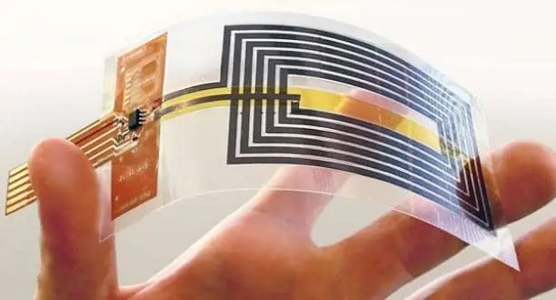
What is an NFC Antenna PCB?

An NFC antenna PCB is the custom designed printed circuit board that integrates the NFC antenna matched to the 13.56MHz frequency along with tuning circuitry to optimize performance. It may also incorporate the NFC controller chip itself or interfaces to connect it.
Key Components:
- NFC antenna – Typically a copper planar coil antenna etched on the PCB matched to 13.56MHz.
- Matching network – Reactive components like capacitors for antenna tuning and matching.
- NFC controller – The NFC controller chip often integrated into the antenna PCB.
- Interfaces – SPI, I2C or UART interfaces to connect to host processor.
- Passives – Bypass caps, noise suppression components for stable operation.
- Connectors – Coaxial cable or board-to-board connectors.
The integrated NFC antenna PCB provides a compact, high performance wireless interface for NFC transactions, device pairing and use cases leveraging near field communications.
NFC Antenna PCB Architecture
Here are some typical architectural implementations for NFC antenna PCB assemblies:
1. Integrated Antenna + Controller
In this configuration, the NFC antenna is etched on the PCB along with the matching circuitry. The NFC controller IC is directly mounted on the PCB.
Benefits
- Compact, integrated solution
- No external antenna required
- Optimized antenna matching
Applications – Wearables, small battery-powered devices like Bluetooth tags/trackers.
2. Antenna + Interface to External Controller
Here the NFC antenna and tuned matching network are integrated on the PCB. Interfaces like SPI, I2C or UART are provided to connect to an external NFC controller chip on the main device PCB.
Benefits
- Allows flexibility to choose external NFC controller
- Antenna can be panelized for production
Applications – Consumer electronics, mobiles, payment terminals etc.
3. Standalone Antenna PCB with Cable
The NFC antenna PCB is a standalone board designed with a cable connector. It connects via coaxial cable to the NFC controller located on another board.
Benefits
- Allows greater freedom in positioning the antenna
- Antenna can be oriented to maximize field strength
Applications – Large form factor equipment like appliances, automotive dashes etc.
The architecture is designed based on physical placement needs, production assembly constraints, enclosure design and other factors.
Design Considerations for NFC Antenna PCBs
NFC antenna PCBs have to be carefully designed for reliable functionality given the high frequency RF signals. Here are some key design considerations:
1. Antenna Design
The 13.56MHz NFC antenna is typically implemented as a planar coil trace on the PCB. Key parameters are:
- Number of turns – More turns increase inductance but require larger board area. 3-6 turns common.
- Trace width and spacing – Typical widths of 1-5 mm are used with ~0.25-1mm spacing.
- Copper thickness – Thicker 2 oz copper improves efficiency.
- Antenna diameter – Maximizing the coil diameter improves efficiency. 25-70mm typical for small devices.
- Geometry – Square or circular antenna geometries are commonly used.
2. Impedance Matching
The antenna impedance is matched to the NFC chip’s tuned input impedance of 13-15pF via an impedance matching circuit. Capacitors are used for the matching network.
3. Tuning
Tuning capacitors like high-Q NP0/C0G ceramic capacitors are used for fine tuning resonance to 13.56MHz.
4. Shielding
A ground plane below the antenna blocks interference from the device electronics. Shielding cans on top provide isolation.
5. EMI Suppression
Filters, beads and capacitors help suppress EMI noise from onboard sources that can affect antenna performance.
Careful modeling in RF simulation tools like Ansys HFSS, validation through prototyping and testing is vital to optimize the antenna design on the PCB.
NFC Antenna PCB Manufacturing Considerations
NFC antenna PCB manufacturing requires attention to quality and process control to achieve design performance consistently:
1. Dielectric Material
The PCB substrate material used must have consistent and stable dielectric properties over temperature variations. FR4, Rogers 4350B, Taconic RF-35 are common choices.
2. Copper Thickness
1-2 oz copper boards are typically used to reduce resistive losses and improve antenna efficiency.
3. Impedance Control
Maintaining tight impedance control over traces is necessary for the antenna coil and matching circuitry. This requires advanced fabrication processes.
4. Registration
Accurate registration and layer-to-layer alignment during multilayer lamination minimizes variations.
5. Surface Finish
Surface finishes like ENIG, immersion silver or noble metals are preferred over traditional HASL finish.
6. Warpage Control
Tight warpage control over the PCB panel is required to prevent antenna detuning or trace cracks/broken connections.
By following robust fabrication and quality processes, manufacturers can produce consistent, reliable NFC antenna PCBs.
Testing NFC Antenna Boards
To validate performance, NFC antenna PCBs must undergo specific testing focused on RF parameters:
1. Frequency Range
The frequency range centered on 13.56 MHz is scanned to check for the antenna response at resonance.
2. Return Loss
Measuring return loss or S11 using a vector network analyzer tests how much RF power is reflected from the antenna. A good antenna has low return loss.
3. Far-Field Radiation Pattern
This validates the electromagnetic field radiated by the antenna in 3D space which impacts power transfer effectiveness.
4. Read Range Testing
Range testing confirms the maximum distance up to which the antenna can communicate with RFID tags or other NFC devices.
5. BER Testing
Bit error rate testing validates the data transmission reliability under weak signal conditions.
Such extensive testing ensures the antenna meets design goals for stable resonance, efficiency, radiation characteristics, data integrity and operating range.
NFC Antenna Integration and Tuning
Once integrated into the final product, additional steps may be required:
1. Impact of Enclosure
The antenna parameters may shift after integration into plastic or metal enclosures, requiring re-tuning with capacitors or antenna geometry adjustments.
2. Snyder Modeling
Modeling per Snyder methodology helps predict antenna behavior when integrated into the final product configuration.
3. Ferrite Shielding
Ferrite sheets help shield and prevent the metallic chassis of devices from detuning the NFC antenna.
4. Production Testing
Sample testing on initial production verifies the design integrates well and delivers consistent performance across units.
With careful antenna integration and testing, optimal wireless performance can be maintained.
Applications of NFC Antenna Boards

The wide applicability of NFC connectivity has resulted in NFC antennas being integrated into many products:
1. NFC Tags
NFC label tags and stickers use printed NFC antenna PCBs to enable proximity based interactions and information transfer.
2. Wearable Devices
Smart watches, bands and trackers often contain compact NFC antennas to enable contactless payments and proximity interactions.
3. Smartphones
Most modern smartphones contain NFC hardware to enable tap-based interactions and payments via digital wallets.
4. Consumer Electronics
Television sets, speakers, home appliances integrate NFC antennas for easy configuring and control.
5. Retail Terminals
Payment terminals like PoS machines utilize NFC reader antennas to accept contactless payments.
6. Automotive
NFC antennas in car dashboards enable features like keyless access, personalization and payments at drive-through lanes.
7. Medical Devices
Wearable health monitors leverage NFC connectivity for easy pairing with smartphones.
8. Industrial Equipment
Rugged NFC antennas enable wireless monitoring, access control and transmission of diagnostics in factories.
With NFC becoming a ubiquitous wireless standard, NFC antenna PCBs can provide short range connectivity across a growing range of applications.
The Future of NFC Antennas
NFC has become firmly entrenched as a mainstream wireless connectivity technology across industries. With advancements in associated technologies, NFC antenna implementations will continue to evolve:
- Smaller integrated antenna designs enabled by miniaturization of NFC controller chips.
- Innovation in antenna topologies like fractal, 3D and ferrite antennas to enhance gain in compact dimensions.
- Leveraging printed electronics technologies like inkjet printing, aerosol jet printing to fabricate simple NFC antennas on packages.
- Higher data rate modes like NFC Boost to increase speeds beyond 1Mbps.
- Combining NFC with other wireless technologies like Bluetooth 5.0 for synergistic applications.
- Use of advanced testing tools like anechoic chambers, OTA test systems and signal analyzers to validate performance.
- Evolution of standards like the NFC Forum specifications and ISO/IEC tags for harmonization.
NFC antenna PCB technology will continue advancing in lockstep with smartphones, IoT endpoints, automotive systems, medical equipment, consumer electronics and industrial applications.
Conclusion
This brings us to the end of our in-depth explainer on printed NFC antenna PCB technology. We discussed the role, architecture, design considerations, manufacturing requirements, testing needs and applications of NFC antenna boards across products and solutions. With the increasing ubiquity of NFC connectivity, NFC antenna PCBs provide the vital wireless interface within devices and systems to enable short range interactions. Advances in integration, materials, fabrication processes and testing will drive further evolution as NFC expands its reach.
Frequently Asked Questions (FAQs)
How is an NFC antenna designed and tuned?
It involves modeling the geometry in RF tools, prototyping, adding matching components, testing key parameters like return loss, radiation pattern and fine-tuning.
What are the typical read ranges achieved by NFC antennas?
Read ranges vary widely based on antenna size from 2-3 cms for tiny wearable antennas to 10-15 cms for mobiles and large terminals.
What PCB materials are used for NFC antennas?
FR4, Rogers 4350B and Taconic TLY offer stable RF performance. LCP provides reliability in flexible circuits for NFC.
What thickness of copper is preferred on NFC antenna PCBs?
1 oz or 2 oz copper thickness is typically used to reduce losses compared to standard 1/2 oz or 1/3 oz foil.
How can NFC antennas be tested for conformance?
The NFC Forum defines standard test processes to verify conformance of antennas and controllers to NFC specifications and standards.
How to choose an NFC PCB manufacturer
NFC is an abbreviation of Near Field Connectivity. This is a simple radio technology that allows the transmission of data held nearby (< 10 cm). NFC technologies are based on the classic RFID of 13, 56 MHz High Frequency (HF)
The NFC standard now enables various transmission speeds of data up to 424 Kbit/s. The main NFC communication method between devices connected is the same as the classic RFID of 13, 56 MHz, which has both a leader and a subject. The master is the issuer or reader, while the subject is a tag or a card.

How is NFC working?
The initiator (emitter) actively produces an RF field via magnetic fields between parallel circuit NFC antennas that may provide a passive goal (Tag).
Emitter antennas and the tag are connected via electrostatic energy, and best this system can be seen as an air-core converter, where the reader acts as a primary winding and the tag as a secondary winding: the alternative charging current through the superior (Emitter) induces an airfield that induces currents into the secondary belt (Tag). The tag may utilize the field current to power itself. In this instance, no battery is needed in reading or write mode to access it. The NFC tag chip gets all power required to function from the viewer’s produced magnetic field via its receiver coil.
What is the usage of NFC Technology?
NFC is an emerging technology that needs to link electrical devices wirelessly. To communicate with hardware devices suitable with NFC and enable new services, such as contactless payment, NFC has been increasingly implemented into devices.
Because NFC tags do not require a power source to be included since they may be driven by the energy the reader emits, it may take extremely basic operating systems such as electric powered tags, NFC stickers, NFC card manufacturers, and even rings.
The compatibility of the chip
First of all: which reader has been used to read or write the attributes. If we cannot read or code a tag, it isn’t very worthy. It is a smart option to confirm that the NFC Chip maker and the NFC Viewer are mutually compatible. See also the NFC Devices Guide.
There are a few factors.
Ø Smartphone
You may pick NTAG® or ICODE® chips if you wish to utilize a smartphone.
Ø ISO14443 vs ISO15693
Whether you use a different reader, it is important to verify if it is the correct one. The chips of type NTAG® and MIFARE® are ISO 14443 and ICODE® of type ISO 15693.
Ø Pre-existing systems
You may verify the kind of chip being used using a smartphone or NFC reader when you are not sure of the technicalities of your NFC Reader but are currently utilizing Microprocessor controlled. You should also ensure that the organization you are using is “open” and enables multiple providers to use Tags.
The inductance of the Antenna:
An NFC tag must have a PCB NFC antenna to connect and be powered. The antenna design process begins with the NFC chip approximate solution and its loop antenna:
- VOC is the open-circuit voltage of the loop antenna caused by a magnetic field
- Ra is the corresponding loop antenna resistance
- La is the comparable loop antenna inductance
- Rs is the NFC chip’s serial equivalent resistance
- Cs is the conventional equivalent NFC chip tuning capability
An inductance La with a very modest loss resistors Ra may define the antenna. When the transmitter in the loop antenna induces a magnetic field, there is a current there, and an open-circuit voltage Voc emerges at its terminals. The resistive input Rs and a built-in tuning condenser Cs may define the NFC PCB chip.
For the final approximate solution of the network containing the NFC integrated circuit and its integrated circuit, the resistors Ra and R are added together.
The NFC IC resistor Rs and the resistive antenna Ra and the built-in condenser Cs create a resonant RLC circuit with antenna inductor La.
The formula shows the frequency response of an RLC series:
- F is the frequency of resonance (Hz)
- L is the circuit inductance equivalent (H)
- C is the equivalent circuit capacitance (F)
The only parameter unknown to the formula is the inductance value L. It is so isolated that it is computed:
The shape of the antenna:
It is feasible to design a loop antenna on a PCB with a certain inductance and geometrically restricted. An antenna may be rectangular, square, circular, octagonal, or even hexagonal. Every form correlates to a particular form which shows the comparable inductivity according to size, the number of rounds, track width, copper thickness, and many other characteristics.
The emergence of internet antenna geometry simulators is an alternative to the laborious computations in the preceding stage. These calculators are manufactured by people or experts and aimed towards
Reduce frequency response. As it is impossible to ascertain the computations made by these internet tools, calculators showing references and formulae used or produced by specialist firms are strongly recommended.
Memory available:
Another key component is the NFC manufacturers have rewritable user memory. The storage should be selected depending on the quantity of data to be used. Labels with less capacity are often less costly.
Here are a few such instances.
- An NTAG210 or NTAG213 chip is sufficient to program a tag with a URL or basic text such as code (containing about 40 and 140 characters, respectively).
- For a computational software business card (V-Card), it is recommended to use a Tag with larger memory, for example, NTAG216.
Tags with a complex framework are also available for specific uses, such as the EV2 chip.
Encryption:
The NFC chip manufacturers give information that is always “visible” without security, viewable to everyone who reads the tag with a smartphone or NFC reader. Just need to use a processor that enables encryption to prevent this.
Open Source Antennas:

Certain manufacturers offer entire solutions for electrical developers, such as designs, application instructions, and even EDA files, to assist the installation of their NFC ICs.
This is the case with NXP, which sells integrated circuits for their NFC range NTAG is a comprehensive handbook with NFC antenna design guidelines and excellent computation software for rectangular and circular antennas, Gerber and Eagle files for various antenna classes.
NXP gives the Eagle data of an antenna produced by its engineers and already implemented in some of its devices for this class. The key benefit of this design is the simulation, correction, and optimization.
Schematic:
The electrical schema is created on EAGLE PCB.
After loading the library “PCB BusinessCard. lbr previously developed, the schematics will include various electronic components.
The built-in NFC NT3H1101, the only active ingredient of the circuit, is coupled to the passive parts utilizing the datasheet specification of its connections.
NFC Quality:

The selection of the correct NFC PCB manufacturer is a significant concern. The term quality may signify a range of various things and is not specified and may be vague in itself.
However, in essence, the NFC PCB quality implies that the panel comes in and draws – no mistakes.
- The quality of PCBs might indicate a multitude of aspects:
- Board in the proper size
- All hole drilled and placed precisely
- Test bare board passes
- Minimum bending of the board (although some of this can be due to board design)
- A lot of additional problems.
The performance should always remain excellent and not decline once the primary orders have been acquired successfully.
As errors might damage the business of the PCB assembly or the equipment maker, confirming the quality of the selected supplier is essential. Other non-competitive firms may be able to enquire about the continuous quality.
Capacity to satisfy requirements:
The first issue is if the maker of NFC PCBs can meet the requirements. In principle, the files may be accepted in the forms they are supplied (typically not an issue, since formats are usually common) and also generate boards with the appropriate specification: number of lines, kind of PCB materials, tolerances, particular requirements, etc.
A comprehensive checklist is worthwhile to ensure they are all able to fulfill them.
Cost of manufacture of PCBs:
The cist is an important element. Cost reduction is part of an effective product. However, attention must be paid to ensuring that the cost is not excessively low.
The lowest cost contributes much to any choice, but it has been claimed that the delight of cheap costs is gone long before the complaint of bad quality has been addressed.
To reduce the total price but for the desired product, the balance between price and performance is essential.
Watch out from Brokers:
It may be surprising that most of the so-called NFC PCB manufacturers are brokers who receive orders and send them to a manufacturing business. Be careful since the standards and regulations that may have to be set on the board cannot be guaranteed.
Although some competent brokers may be able to place orders that are helpful in general, the best thing to do is guarantee that the genuine NFC PCB manufacturer communicates.