The behavior of the chip antenna is very unpredictable since an antenna can function when used as a facility for testing and when it is finally integrated into the device. However, we cannot say this about antennas.
What Does a Chip Antenna Mean?
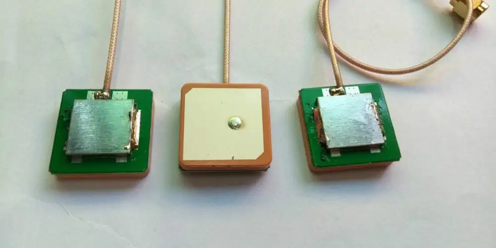
The chip antenna is a unique antenna, well-known for a compact footprint. In order to emit high frequency electromagnetic waves, they are frequently incorporated in circuit boards. They are ideal for tiny devices such as mobile phones and WiFi routers due to their constrained range.
The main distinction between the ordinary antenna and chip antenna is its tiny size, although both can transmit and receive electromagnetic waves. Taking their quality into consideration, they are not expensive. Whenever the larger-sized antennas are not feasible, the antenna on chip is the best option.
Making use of fractal geometry is a reliable way of designing an antenna to be added to the printed circuit board. This fractal geometry can be described as a complicated pattern created by repeating a basic form that lengthens the material’s perimeter or optimizes the length of that material emitting electromagnetic radiation.
These antennas should match the wavelength of the signal; also, the fractal pattern must be preserved in at least two distinct ratios. These antennas, which can be tailored to fit different footprints, can also be seen in mobile gadgets. Generally, fractal antennas have remarkable bandwidth and gain. The designs for fractal antennas don’t require any additional parts to function. This ensures its flexibility further.
The Design of Chip Antenna
Chip antennas provide small and portable solutions for wireless products. They simply require a little room and some ground clearance. Users receive performance which is marginally inferior to those of larger antennas including PIFA, patches, as well as dipoles in exchange. However, there are some limitations that you need to take note of.
Watch out for the ground planes
Actually, a chip makes up just half of an antenna design. The PCB’s ground plane constitutes its other half. Similar to the monopole, the form as well as size of ground planes have a direct impact on the pattern of radiation as well as tuning of the antenna on chip.
The majority of datasheets will list the antenna’s maximum gain, return loss, bandwidth, radiation pattern, as well as other characteristics. They would also comprise a drawing. Have you noticed the PCB’s dimensions? Measurements taken from this specific ground plane served as the basis for all reported performance numbers. It’s quite possible that the chip antenna that you incorporate into your device will fit onto a PCB with a different dimension. Hence, the performance will be different from what is shown in the datasheet. Also, since the performance evaluations were conducted outside, the antenna will probably be contained within a product.
Layout for the Chip Antenna
Note that you can only place metal near the chip antenna on specific sides. You should position the chip in one corner only with the ground on both sides. It is wrong to position the chip through the three sides, which now becomes perpendicular to the earth.
As previously mentioned, the antenna would be impacted directly. Performance declines when the ground becomes closer than usual. Performance also changes when the ground gets farther away than normal.
Differences between the Printed Antennas and the Chip Antennas
What does printed antenna mean and how does it work
Your PCB is useful for printed antennas, commonly referred to as microstrip antenna. They are also composed of a unique geometric design located on the top region of the copper plane with precise lengths and widths to fit the impedance and frequency of the emitting circuit. Many patterns, such the inverted F, circular, straight trace, and others, are relevant in this case.
The printed antenna could be thought of as a simplified, scaled-down variation of the conventional wire antenna. With respect to the dimensions of the microstrip traces and copper planes, this can hold different frequencies and impedances.
Understanding the chip antenna
Chip antennas are constructed as dielectric-filled ceramic cavities between conducting surfaces known as the dielectric resonator antenna (similar to the way ceramic capacitors are built). It produces the stationary wave and is referred to as the cavity resonator. Similar to PCB antennas, this same impedance and frequency also depend on the shape of the conducting surfaces, but because the materials have a high permittivity, the antenna’s size for same wavelengths could be reduced significantly.
Asides how both antennas were built, how do they differ?
During the development of both antennas, there were some factors to consider. The most obvious of all these factors is the size. It is important to take note that relative to making use of the chip antennas as a tiny component, designing with the use of printed antennas needs a larger space for the traces and copper planes.
Another important factor is the climate and temperature. The electromagnetic interference of close circuits will most likely affect the printed antennas. Also, the antenna region must stay free from all conductive components and traces across all levels since the metallic objects close to the antenna’s irradiation area, including all other copper layers on the Circuit board, might limit the performance.
While 50% of the performance and effectiveness of the chip antenna depends on the execution of an efficient ground plane, the chip antennas are less susceptible to this problem but tend to become more delicate towards the noise that originates from the ground planes.
What is the Performance of the Chip Antenna?

The effectiveness of the chip antenna would be changed significantly by the following factors. Let’s quickly consider each of them.
Layout
The effectiveness of the antenna on chip is significantly influenced by how the components are spaced and positioned on the printed circuit board. Chip antennas should have ground planes that have the right size and are well located in order to create a full resonant circuit.
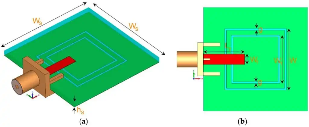
A dipole would be created by ground planes with a length of 3 to 4 cm, as well as a breadth of 1 to 2 cm. However, if this plane is larger, it would act or function as a monopole antenna. This PCB can function as a ground plane. However, the antenna itself has to be mounted and placed on the edge of the printed circuit board. This is located on the top section, which is isolated from the remaining parts of the board and free from metal objects that could affect or interfere with its radiation.
Moreover, both the microstrip line and ground plane has to be proportionate. The feedline must be as short as possible in addition to being perpendicular to the microstrip line. This is to avoid becoming a parasitic component of the resonance system. The vias, which are carefully positioned through the holes in the board, helps in reducing the electric field created at the edges of the printed circuit board.
Panel chip antenna selection
Because of their widespread use in many portable devices, chip antennas were built within rubberized or polymer enclosures. This helps in shielding the circuit board from some damaging elements such as stress, vibration, dust, moisture, or chemicals.
Casings and metal parts should be kept to a minimum. In addition, the radiation pattern of the chip might be affected by these enclosures and casings. This is why they have to be examined properly and carefully.
What are the Benefits and Drawbacks of the Ceramic Chip Antenna?
The use of ceramic antenna comes with different advantages. For instance, it reduces the need for modeling software and takes away the expensive fabrication of fresh prototypes. This is because the antenna lacks physical qualities and needs network tweaking. Generally, this is economical because you won’t be wasting components as a result of continuous prototype manufacturing.
Other benefits of the ceramic antennas include:
- It has different setups
- Reduced size
- It is less susceptible to noise from components and the environment
- Ceramic antennas accommodates modifications to the design guidelines of the PCB design guidelines
- It is less simulation-intensive.
- It is very easy to replace
However, ceramic chip antennas have some negative side-effects. These include:
- Higher initial costs such as the purchase price of the ceramic chip antenna as well as the need for its auxiliary components. The cost per unit ranges from around $0.10 to $1.60 on average. However keep in mind that this is an average price, not its maximum price.
- This PCB trace antennas performs better compared to the ceramic chip antennas.
Overall, because a ceramic chip antenna is introduced to a circuit board after the phase of the design has been completed, it offers more tuning flexibility. As they use the surface mount arrangement, they also allow quick hardware upgrades.
The ceramic chip antennas allow you greater room as well as openness in the design. This enables the usage of further components for every stack. Also, this enables the utilization of smaller printed circuit boards as well as the addition of more components. This results in a better overall cost-effective design. Moreover, you will definitely see a huge rise in savings if you have a multilayer design.
What Does Antenna Matching Mean?
Antenna matching can be described as the process involved in modifying the design so as to ensure the other radio frequency circuits on the PCB and the antenna’s (module or chip) impedance are properly matched. To construct an effective and productive antenna, this impedance should be around 50 ohms. This is because interference from nearby components on the PCB or the housing can alter the frequency of an antenna.
One reliable method of achieving this is to include the impedance matching circuits in the design. Antenova advises using the pi (TT) matching circuits so as to allow the tuning as well as optimization of the antenna. For the single band antennas, pi matching circuits may include three components (capacitors and inductors), or even more for the multi-band antenna. Also, this serves as a helpful approach to adjust an antenna’s performance within a design, especially in practical situations when the antenna must work in less ideal locations, including while being held in the hand and worn on a person’s body.
Furthermore, the co-planar grounded wave guide advised whenever the embedded antenna is placed on a PCB. This eliminates the need for vias, which is preferable because they contribute loss to a transmission line as well as inductance into these matching components. This leads to erroneous tuning values.
Market Trends for Chip Antennas
Chip antennas are small antennas that transform radio waves into electrical signals and vice versa. The proliferation of the chip antennas in the IoT devices, a rise in the demand for the smart antennas, the prevalence of internet, the rise in Smartphone usage, and improvements in the 5G technologies were the main factors propelling the market’s expansion.
However, the lack of a consistent frequency spectrum for different wireless applications could impede market expansion. On the other hand, over the projected time, the development of the 5G technology will present an enormous chance for expansion for chip antenna markets. On the grounds of end user, type, application, and region, this chip antenna market can be broadly categorized.
The dielectric chip antennas and LTCC chip segments of the market are separated by type. Bluetooth chip antenna, multi band/dual band, GPS/GNSS (gps ceramic antenna), WLAN/Wi-Fi, nfc chip antenna and other applications make up this application segment. This market is examined by the end user and also broken down into segments like healthcare, consumer electronics, automotive, and telecommunication.
Conclusion
We hope we have been able to explain what chip antennas are. Antennas, which form the major components of the RF devices, have a huge impact on the way they work. The main criteria for current RF applications are high performance, reduced size, as well as reduced cost. There are many advantages to using the Ceramic Chip antenna. The most important of all is that it does away with the need for pricey simulation and prototype production softwares.