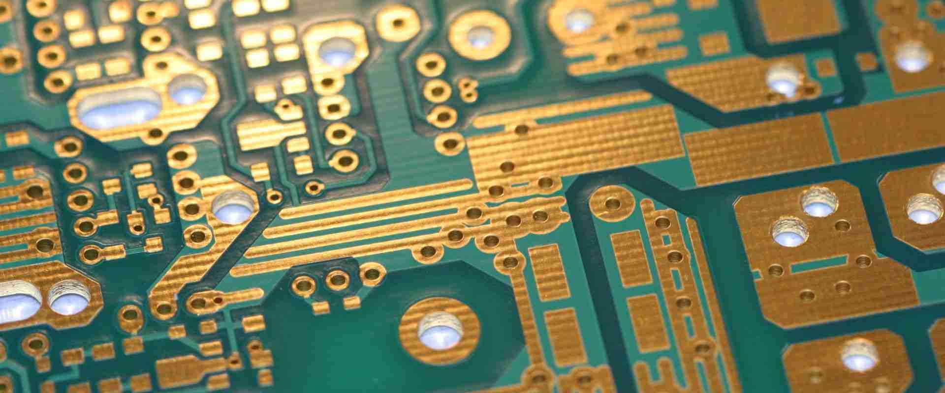
The printed circuit board is a flexible element used across various industries. Its acceptance cuts across the technology and the electronic industry due to its unique attributes. Its copper density is a crucial factor in fabricating a standard PCB. The conductivity role played by the copper is essential to the Printed circuit board.
The Printed circuit board depends on electricity to carry out its infinite functions. The nominal circuits in the board are the pathways by which electric currents move from one place to another without hitches. Copper is a standard carrier due to its conductive nature.
The copper performs well as a high conductive component. It is possible due to the valence electron it possesses. Electrons convey electrical signals that form the foundational particles which hold electrical charges. The copper density carries the electrical signals without ditching electricity.
Furthermore, Copper density is also known as copper thickness or copper weight. It is in the sq ft. area of the circuit board. The Coppers’ measurement is in ounces (oz/ft₂). Its thickness determines the current-carrying strength of the whole Printed circuit board.
Making a wrong choice of copper density during the PCB designing process could ruin the performance of the PCB. Thus, understanding the connection between signal conductance and copper weight is crucial. It would help make the right choice of copper density for the PCB.
The thickness includes 0.5 oz copper thickness, 1.0 oz/sq ft copper thickness, and other types of density measurements available. Going through this article will help deepen your knowledge of PCB copper density. It will also supply adequate information on various copper densities.
Copper is one of the essential components of a printed circuit board as a great conductor. Choosing the perfect copper weight type during the fabricating process helps avoid issues that could affect the functionality of the PCB. The copper is a strong basis on which the PCB thrives. It serves as the connector of every component around the circuit.
Electronic designers mostly relegate components such as the PCB copper weight and the board thickness to the background. The copper density adds to the whole thickness of the external layers of the PCB. Its importance is significant to fabricating a standard PCB.
The copper density or weight are of three different specifications. Each classification has its analytical role in the PCB manufacturing process. As a very strong conductor of current, its measurement is in ounces per square foot.
Classification of the Copper Density
Standard Copper Weight
This copper specification ranges from ¼, ½, 0.5.oz per sq ft to 4 ounces per square foot. It has been the measurement in use for a very long time. Using this type of copper density reduces the risk of failure in the printed circuit board.
Heavy Copper Density
The weight for this kind of copper density ranges between 5 to 19 ounces per square foot. The heavy copper surpasses the standard copper in diversifying the PCB design. It offers more room for creativity and experiment.
Extreme Copper Density
This density weighs around 20 to 200 ounces per square foot. To fabricate long-term designs, designers choose an extreme copper density. It involves laying two copper densities on a single PCB layer. Also, it removes the need for several standard copper plates. It also enables designers to place a small quantity of extreme copper on the exterior layer of the board.
The extreme copper density on the PCB allows the carriage of more current. However, there are other copper densities available. They include:
What is 0.5oz PCB Copper?
Several PCB designs require specified copper density to meet the electrical current demands of the circuit. To choose an appropriate copper density to fit the design hinges on the type of PCB. The 0.5 oz copper thickness in mm is also called ½ oz copper thickness. It is the copper measurement type that forms part of a non-standard fabrication. It is obtainable in the inner layer of the design.
The 0.5 oz copper thickness approximates a piece less than 0.0007mm. It is an uncommon option for small products and appliances with less conductivity. The size of this copper type is a unique option among manufacturers. Its thin size exposes the design to overheating in contrast to other copper weights.
It is important to note, designs that require 0.5oz or 1.0oz’s electrical difference are trivial. The copper thickness in the circuit board does not have a standard measurement. Fabricators could choose the perfect fit for their design. It could be at 0.5oz/sq ft or 1.0oz/sq ft thickness.
The main difference between the copper thicknesses and other types is the direct current resistance. PCB with a high copper foil impacts the direct-current resistance on the planes and traces. Therefore, dispersing direct current around a large PCB, there could be a voltage drop.
It is the primary density for the printed circuit board. Having sufficient copper in the design secures a perfect working condition in the PCB. The 1 oz thickness is the standard copper density on the outer layer of the PCB. It is one of the most popular flex PCB copper weights.
2 Oz Copper
A 2 oz copper PCB is a design that has a copper weight per square foot at two ounces. It is the internal copper density of the inner layer in the PCB. It is on a 3oz complete copper selection. The 2 oz copper is perfect for appliances with bigger current demands.
Fabricating a bulletproof PCB with high capacity requires heavy-weight copper. This type of copper density is highly reliable, and it has comparative advantages over the thinner copper types.
Conclusion
By now, you should have gained much knowledge about half oz PCB. Copper is an exceptional conductor, and it plays a crucial role in the fabricating process of the PCB. Therefore, choosing the perfect copper density to suit the application is essential. A wrong choice will deter the performance of the board design.
One of the ways to improve performance is through increasing the operating speed. Taconic now offers a platter-type PTH with a flywheel drive that achieves superior efficiency. It does this by generating energy at twice the normal speed and returning it. We can achieve a small size thanks to PCB technology with this improved performance and design.
The new PCB design produced by RayMing PCB and Assembly goes even further by combining vertical and horizontal power supplies. This results in increased flexibility and easy replacement of individual power supplies without disrupting the flow of electricity throughout the machine. It offers these features combined with the audio and data functions and low power consumption expected of a PTH. IF NECESSARY, the PCB can be easily removed or replaced, making this PTH appropriate for use in critical areas, such as hospitals and hotels.
Another essential feature is the “auto-power on” function. If we do not use this function, there is still no need to connect an AC power source to start up the machine.
The high-performance Taconic TLF-35A also features a lightweight, compact body that we can easily carry and install, a large LCD, and easy operation.
An interesting detail here is that you do not need a power source to start up the machine.
The time from power on to final buffering can be as little as six seconds.
One main objective of the Taconic TLF-35A is to reduce power consumption by as much as 30% compared to conventional PTHs. For example, a platter-type PTH such as the Taconic TLF-35A uses only 10W at maximum, compared to 20W or more in a platter-type PTH. On the other hand, other functions use lower amounts of power. The PCB design is another essential factor in the reduced power consumption. We can easily replace the PCB of the Taconic TLF-35A with another PCB.
Even when we make a replacement PCB, it takes only 60 seconds or less to get the machine up and running.
Another essential feature is the auto-power on the function that starts up the machine immediately at power on. There is no need to connect an AC power source with this function.
The auto-power on the system allows operation in environments where fluctuating power might influence how long it takes to start up. In addition, we can use the machine with a remote-control unit, if necessary.
The PCB allows for a low-cost installation of the tray. Also, we can easily replace and the motors. We install a new PCB in only 60 seconds or less to get the machine up and running.
Size
Compared with other PTHs with platters of 35cm in diameter, there is only about one inch more of playing surface on the Taconic TLF-35A. The PTH weighs only 3.5kg, less than 4kg (certainly lighter than most conventional PTHs).
Many companies build Laser pickup and servo control into the Taconic TLF-35A.
The Taconic TLF-35A is also small compared to PTHs with a bevel-type data system.
This PTH is small enough to transport by hand.
We can remove the top and bottom covers by loosening the thumbscrews on both sides of the platter. Then, we install a new PCB in only 60 seconds or less to get the machine up and running.
The Taconic TLF-35A is so light that one person can easily carry it, making it convenient for carrying and moving.
The LCD (1.6 inches) shows pitch, rpm, and track numbers.
Why you should use the Taconic TLF-35A PCB
The Taconic TLF-35A PCB is a very convenient product. You can easily carry the PTH and install it in the customer’s location. In addition, the time required to start up the machine (after power-up) is less than six seconds.
Suppose there is a problem with one PCB, only that PCB needs replacement, and then we can use the PTH immediately. There is no need to replace all of them, as in other machines.
1. Very high thermal reliability
Because the PTH is small, we can use it on a desktop or a shelf. Consequently, the thermal design is very critical. Also, because the main power supply uses an inverter, there is not much margin for error in heat. Basically, with other PTHs such as conventional ones that use a bevel type data system, this would not be an issue if the signal does not drop off too much, not enough to cause problems.
2. Compact and portable design
The Taconic TLF-35A is so small that we can easily carry it around. It weighs only 3.5kg which is very light compared to most conventional PTHs. Its size is only about one inch larger than a conventional PTH with a platter of 35cm in diameter, although the playing surface is much bigger since it has a platter of eight inches in diameter.
To move around, you can carry the Taconic TLF-35A by hand or place it on the shelf. We do not need any special vehicle. We can easily install it in difficult-to-access locations because of its compact design and lightweight.
3. Low moisture absorption
The highly conductive PCB makes the Taconic TLF-35A suitable for hotels and hospitals where the environment is not very stable.
No matter how long it has been sitting in a customer’s location, if there are problems with the PCB, we can easily replace it and use the PTH again immediately.
4. Exceptionally low DF
Reducing the attraction force is very important for this type of PTH. Also, since the PTH is so light and small that we can move around quickly, it is essential to ensure it does not move unexpectedly. The built-in optical sensor in the platter provides exceptional accuracy.
The Taconic TLF-35A has a DF of less than 2m (1/3N). This is a very low value. DF is a standard measure of the amount of force that pulls a disk in one direction.
5. Low-noise turntable
The Taconic TLF-35A uses laser pickup and servo control, with very little noise and high stability. We must replace the PCB when there are problems with performance since there is no need to replace all of them as in other machines.
6. Excellent peel strength
Peeling a CD is not difficult if the force on the disc is strong enough. However, many paths have problems with this. This problem is that each platter in a conventional PTH has a separate motor for rotation and thrusting. This type of machine makes a great deal of noise during peeling.
The Taconic TLF-35A uses one motor to do both, so there is little noise and excellent stability during peeling.
7. Low cost
The cost of the Taconic TLF-35A PCB is much lower than that of a conventional PTH.
Each cartridge (platter, motor, pickup, and PCB) costs approximately $300. So, if you purchase them in bulk, they cost less than $100 each.
The Taconic TLF-35A is excellent for use in any place where the environment is not too stable. Also, the Taconic TLF-35A provides excellent performance. So, we can also use it to play audio CDs recorded with a PC and not with a CD recorder, as usually is the case.
This is an automated PTH that can play audio CDs and not record them. For example, if you want to playback songs stored on your computer, you can use this machine.
1. Filter, coupler, splitter, combiner, and mixer
We can use the Taconic TLF-35A to route audio signals. The built-in optical sensor makes it easy to align the disc with the sensor, and therefore, it is easier to plug into any system. (The coupler, splitter, and combiner work the same way.)
2. Antenna
The Taconic TLF-35A has a pre-amplifier and a mixer that make it easy to connect to an antenna. We can use this type of PTH for a PC or other device with an antenna such as a TV or VCR.
3. High power Amplifier, TMA, TMB, LNA
The Taconic TLF-35A is significant in high power amplification. We can achieve this by using the TMA. Generally, we need a high-power amplifier when we use an antenna as the input source of the PTH. The TMB is also available if required.
To connect to a PC via a S/PDIF interface, we must connect a digital transmission receiver that uses the USB interface to the “SPDIF Out.” We can achieve this by using the TMB.
4. Power Supply
A power supply is not required since the main power supply is an AC inverter. The DC input is 5V and 100mA and can power a PC with a USB interface if necessary (for example, to connect to the PC via a S/PDIF interface). Also, we can use the USB interface for data transfer from a PC to the PTH.
5. Repeater
The Taconic TLF-35A has a built-in repeater, so it is possible to connect to the Taconic TLF-35A by using an antenna and from an antenna. This is possible because of the flexible design of this PTH. The default settings are connecting the PTH to an antenna, but if you want to use the wireless LAN function, “Wireless Control” is available. This mode uses a wireless connection using the 802.11b standard.
6. Passive components
It is possible to use a 100V switch mode or a standard AC power supply. The power consumption is approximately 4W.
7. Decoupling circuits
Many electronic components contain some static electricity. Some of these components can reduce static discharge when used in sensitive components such as CD players. Using these parts can prevent damage to the sensitive components when used under specific conditions.
8. Medical scanners
We can use these to read the medical data from a patient’s pulse, etc. These medical scanner designs are industrial PTHs. This type of PTH has many functions and can apply RF energy when necessary.
Conclusion
A significant feature of the new Taconic TLF-35A is increasing performance through PCB technology. The Taconic TLF-35A is ideal for use in hospitals and hotels. We must always connect an AC power source because it can be easily handled and transported, and we can remove the AC power cable when not in use. The new Taconic TLF-35A comes with a three-year warranty period.
The PIMD, not unlike the predecessor TLF-35A, will produce some of the best-sounding music you’ve ever heard in your vehicle. The Taconic has only four channels and has a PLL design susceptible to radio interference. We can nullify this radio interference by using a soft muting feature in which the unit mutes for about two seconds to clear out noise in the radio frequency area.
The fast pace in technology development has brought innovations in Bioengineering. These innovations have also given rise to many software-based devices. The devices can help control the current patterns of human activity. The medical field is by far the leading consumer of these devices. The demand for such equipment is so high. The high demand it has prompted several companies to develop new designs. They are also developing designs for their products in the reaction. Companies such as Rayming PCB & Assembly have developed a modernized product line design to meet their consumers’ demands. Their new device is a lightweight EMG monitoring system. They have unique designs that we can explicitly use in hospitals or other medical facilities. Medical professionals continuously monitor a patient’s heart rate and blood pressure levels. It is easy to know what jobs using EMG sensor, you can do.
What is an EMG sensor?
An EMG sensor is a small device used to monitor the electrical activity of muscles. Medical professionals use this device to help diagnose patients suffering from muscular pains. The frequency of electrical impulses generated by the muscle can tell the physician a lot about how injured the patient’s muscles are. This will inform what type of therapy they may need to accelerate their recovery process.
Historically, physicians have been monitoring muscle activity through direct contact. They use electrodes placed on the patient’s skin. Such methods have provided accurate readings during the monitoring process. But they are highly invasive and time-consuming. This made such methods unsuitable for long-term monitoring and treatment.
For this reason, medical professionals decided to use ultrasound to help track muscle activity. Medical professionals can see a live ultrasound feed on the track. This allows them to directly assess the muscle movements of their patients from a safe distance. This made monitoring patients’ muscle activities much easier. It also significantly improved their recovery process in most cases.
EMG sensors use one of two methods to monitor muscle activity. You may design them to pick up ambient signals from the patient’s muscles or have electrodes embedded into them. We usually pick up the ambient signals using a combination of the surface. Additionally, we apply fine-wire-based electrodes directly onto the patient’s skin. Then, The EMG sensor picks up the signal, which the medical professional may hold. They may also attach it to a wearable device such as a holster-like strap.
1. sEMG sensors
We can also refer to it as the surface EMG sensor. These sensors can pick up the electrical activity from muscles and tendons within an entire body. We do this type of monitoring by covering a patient’s entire body with electrodes while placed in a prone position. The result is that we can covertly monitor the entire patient’s movement when fully clothed. The advantages of using the sEMG sensor are lightweight and very portable. They are also easy to use by medical professionals. Several professionals are conducting numerous research on this type of EMG sensor. They are much easier to troubleshoot when problems arise. The main drawbacks of sEMG sensors are that they have limited life cycles. This is in comparison to other types. If ripped off the patient’s skin, they are easily damaged and rendered useless.
2. Intramuscular EMG
Physicians usually place these are EMG sensors directly into a patient’s muscle. They monitor the muscle movements on such a close level. It helps them tell when there is an increase or decrease in blood flow to certain areas of the patient’s muscle. They use this type in patients with acute or chronic wounds and injuries. They also use it for other related conditions for which long-term monitoring of the patient is necessary. This type of monitoring allows medical professionals to assess the condition accurately. It also helps them track and progress of the patient’s healing process.
3. Deep Tendon EMG
We often refer to this type of EMG sensor as muscle biopsy. It is similar to the sEMG in many ways. The only major difference is that this type monitors mainly tendons. The deep tendon EMG has been around for longer than the sEMG. It is more reliable in terms of quality and accuracy when compared to other types of EMG sensors. The main drawback of this type of EMG is that it needs a very highly trained medical professional to apply and monitor it. This makes the monitoring process of patients in an acute state extremely difficult.
4. Intracortical EMG
This type monitors signals from the cortical neurons within a patient’s brain. These sensors are usually applied to the brain’s motor cortex using a craniotomy. We can also apply their other surgical procedures. It allows doctors access to the area underneath where they can apply the sensor directly onto the part of the cortex. We use this sensor mainly to monitor and detect changes in a patient’s motor skills. It primarily applies to patients whose injuries may be too extensive for sEMG sensors to detect accurately.
How EMG sensor work
If you was to learn how to make EMG sensor, you first need to understand how it works. An EMG sensor is a small, lightweight (usually less than 1.6 ounces) piece of medical equipment placed on the patient’s skin. We typically connect the EMG sensor monitor to the patient. We use a cable that connects to the patient’s computer or a specialized package that connects directly to the patient’s computer. This format enables the monitoring of usable data from multiple patients at once. It also offers an easy way for users to exchange data from one set of monitors to another.
The EMG sensor works by getting close to the patient. Since it is small and light, we can easily place it on the patient’s skin. Once connected to the patient’s computer, any change in the electrical activity of muscles triggers an alert signal. So, we can send it via email or through a wireless application at home. The EMG monitor then provides medical professionals with crucial information. The information can help them make critical medical decisions in their patients’ best interests.
We can make an EMG monitor using different components. It can consist of a kit that allows users to monitor a few muscles in the patient at once. We may also design other monitors to monitor many muscles simultaneously. Usually, the larger the area we monitor, the more complex and expensive the design.
These devices generally consist of medical-grade plastic that is lightweight and durable.
Software Interface of Arduino-based EMG sensor
A software interface is a computer code that facilitates various hardware devices. An example of this would be the interface between a computer and an internet security system. With many commercially available products such as Arduino, we must make the interface case-by-case.
For example, one may want to connect to an EMG (electromyogram) sensor. They may also not connect it to other bio-telemetry sensors that do not offer standard protocols. These are protocols required for easy integration with standard programs on the market today.
We can sample the Arduino analog input using the analogRead function of Arduino. We can use the Arduino to read the signals from the EMG sensor and send them to a PC for processing and analysis. The apparatus used in this project is a simple EMG amplifier circuit that they built and amplified for use with an Arduino (Arduino). The amplifier amplifies the received signals 100 times. This easily transforms them into a digital format that software can record and process. The ADC (Analog to Digital Converter) is the device that converts an analog signal into a digital format. The ADC uses a series of switches to measure the voltage coming from the sensors. Then flip it into binary values displayed on a PC screen. We need to install the driver for our Arduino board to have a functional connection with the computer.
The Interface Circuitry
One can make the interface circuitry for the Arduino of 16 pins, as shown in the figure. We use the first eight pins to connect the Arduino to the PC.
We use a voltage divider circuit to measure voltage. This is the voltage coming from two previously connected sensors and amplified multiple times (100 ×). In our case, we will be using two sensors to reproduce a signal that can track whether a person is in pain. We will use the first sensor to track the rotation of the thumb, and the second sensor will monitor the movement of the index finger. We use the voltage divider circuit to ensure that we can measure any change in output value that is coming from our amplified sensors. This circuit is a very simple but effective way that helps us capture a signal that we can easily process by using Arduino software.
We can connect the Arduino to the PC using a USB cable. The board has a built-in power supply that uses the 5V pin to power the circuit and charge the battery. We will also have to connect a small motor to create real-time results. Then we can use it to simulate a finger movement and track if it has caused any movement in our thumb’s joints and muscles. The Arduino provides us with processing information from the sensors to send it to our computer.
We must handle all electrical equipment, including medical devices, with care and caution. When dealing with high voltage electronics, there is always a risk of electric shock that any exposed part of the device can cause.
We should always turn off the electrical connections when not using them. In this situation, we connect the Arduino board to the computer via a USB cable to transmit and receive data over a computer network. When we don’t need this data, we can disconnect it.
When working with any electrical devices, be sure to use protective equipment such as rubber boots and rubber gloves. This ensures that the user remains safe from any possible electric shock while handling the equipment. You should always keep any exposed wires on the device from the user’s body during operation to avoid possible electric shocks. The general rule for working with any electrical device is to avoid touching the exposed wires with the body. Ensure that you use protective equipment whenever needed.
Safety is essential when working with high-power devices such as an EMG sensor. This device delivers a large amount of electrical current. So we must handle it carefully. It helps us avoid possible contact burns or any other harmful effects from improperly handling this equipment. It is essential that the user read all safety warnings before using this equipment. They should always follow all of the manufacturer’s safety precautions.
Essential components
Connecting Wires & Jumper wires: If a servo motor is in use, you should also power the Arduino. The Arduino cannot power the motors directly but only send power through a power supply circuit. Similarly, if you use a small motor, you should power it using a separate power supply.
9V batteries: Using 9V batteries to power the Arduino is not efficient. It is inefficient, especially when powering it with a battery charger and a DC source from an external source such as a wall socket.
A 3-lead connecting cable: We use this for connecting the circuit to a PC. You will need 13 cm of cable for each connection.
52mm electrode pads: These are electrodes attached to the skin. They consist of conductive gel and offer a reliable connection to external electrical equipment.
AD8226-based EMG sensor: It is one of the most common EMG amplifiers used in EMG sensor projects. This device can amplify and convert the EMG signals from the electrodes.
Arduino UNO: This is an Arduino board that we can use in various projects. It is one of the most popular and easiest boards in building projects based on hardware.
Arduino IDE: This program file allows the programming of Arduino to use a graphical user interface. The IDE’s code editor also provides syntax highlighting and auto-commenting tools for any code written by the user.
Arduino code: We then upload this code onto an Arduino board.
Interfacing EMG Muscular Signal Sensor with Arduino
We use EMG sensors to monitor muscular activity in humans and animals. Data is continuously acquired from the sensors by a computer. You can then process it and interpret it into helpful information.
This process involves processing signals from the electrodes. Then, you amplify them before translating them into a form that another system or machine can understand. This form of data is also called an EMG signal, muscle signal, or muscle event.
1. Electrode Connection
We apply the electrode pads to the skin of a subject. Then, we must connect these electrodes to the EMG sensor through a connecting wire. We frequently do this by placing one of the electrodes between two metal contacts placed on the EMG sensor circuit itself. The connecting wire is then attached to these metal contacts. This completes the circuit. It allows for the reading of EMG signals by the sensor.
Yellow electrode:
This reference electrode allows the Arduino to determine which electrodes we are using. We place this electrode on the skin between two other electrodes and act as a reference point. You must also connect it to the sensor’s power supply to get a stable reading.
Red electrode:
We use this electrode to measure the activity of the muscle. You must place it over a muscle and connect it to an amplifier via a wire. The amplifier amplifies the signal and sends it to the sensor.
Green electrode:
This is another reference electrode that acts as a reference point for the Arduino. You do not need to apply it over any muscle since it does not record muscular activity. Also, you do not need to connect it to the power supply since this will not affect its performance.
2. Power Supply Connection
We also connect the power supply for the electrodes and the amplifier to the Arduino board. This allows for signals generated by the Arduino board and sent to the sensor via the connecting wires.
3. Motor Connection
We connect the motor to a power supply to provide a steady flow of electrical current. We can adjust the current speed by adjusting the power supply’s voltage or by adjusting the resistance between its two terminals. To prevent the wrong movement while sending electricity through it, you need to adjust the resistance.
How to code a EMG sensor
“The Arduino UNO” is an Arduino board that we can use to build a prototype of an EMG sensor. The Arduino board has a built-in circuit that can read the values coming from the sensors and then process them using the software.
Reading the data straight from the sensors allows for quick evaluation of processed information. This removes all kinds of delays. To do so, we need to connect our circuit to our computer via USB cable and upload a program onto the Arduino. Programmers usually write this program specifically to adapt to any other purpose easily. We can find the provided code under the tab “Code.”
A significant challenge of using EMG sensor Arduino is that it requires a large amount of knowledge. You also need a lot of experience with the program and its environment to get the most out of it. Compared to other ready-made hardware, Arduino offers us a lot more control over its internal components. They are completely open-source. Another advantage of using Arduino is building complex projects. We use it primarily for more advanced projects and applications.
“Muscle activity” controls one or more muscles to produce the desired effect. For example, speaking, lifting, or kicking. We measure it by recording the electrical activity generated by a muscle. One can do this by tracking the resulting change in electrical potential present in a muscle.
1. Muscle activation and electrical potential change
Muscle activation refers to the movement, or contraction, of a muscle. Several factors including: can cause this movement
Muscle force is the amount of force applied to a muscle. You must increase muscle force by making the muscle work harder or decreasing its resistance. One can reduce the resistance through relaxation of the muscle or by lengthening its antagonistic muscles.
Some muscles have an inherent property that causes them to contract when stretched. We refer to this as a reflex action, and it is a common phenomenon present in human beings and animals.
A muscle can exert force to overcome the external resistance exposed to while contracting. This resulting force has an inverse relation with the square of the muscle tension.
Muscle contraction and relaxation are both affected by signals sent from other parts of the body, such as:
2. Muscle action potentials
When a muscle contraction occurs, the muscle activates and then relaxes. The body sends electrical signals from the muscle to the nerves surrounding it during this time. These signals contain information about muscle contraction and pass it on to other body parts. The atrial and ventricular nerves are responsible for sending these signals. However, not all muscles have a direct nerve connection to them. For example, many nerves that connect directly to other body parts, such as the spinal cord or brain, supply many muscles in the body.
3. Recording EMG signals
We can use several methods to measure the electrical activity of a muscle. These methods range in price, complexity, and precision. The most basic way of measuring muscle activity is by placing electrodes on it or around it. We connect these electrodes to an amplifier. Then, a computer reads the resulting signal. This method is common in hospitals and laboratories due to its relatively low cost, ease of use, and accuracy.
4. Processing EMG signals
We can measure and record muscle activation in real-time. The EMG muscle sensor ensures that we do it with a relatively high level of precision. However, these measurements cannot accurately evaluate the muscle actions themselves. This is where the processing of these signals comes into play. We can process the data in several ways depending on the type of activity that we are recording.
The above techniques use numerical methods to evaluate each signal. So they tend to be more complicated and less effective than other techniques.
Conclusion
EMG sensor is a potential solution for human movement and speech recognition. The main advantage of this system is the accuracy of the measurement. Human movement and we can measure speech with a high level of precision. Also, this system is relatively inexpensive. It makes it an attractive choice compared to other available systems and methods. Wearable EMG sensors are also a cost-effective solution for monitoring respiratory function. We use these sensors throughout the respiratory system. They can provide valuable information to the user on respiratory status.
The EMG sensor proves to be a valuable tool for researchers. It helps collect knowledge. It also provides new insight into improving human movement and optimizing speech recognition.
Rotary encoders, also known as shaft encoders, are electromechanical devices used to convert the angular position or motion of a shaft into digital signals. They are used in a wide range of applications that require precise shaft unlimited rotation including industrial controls, robotics, consumer electronics, automotive, aviation, and medical equipment.
How rotary encoders work?
The working principle of rotary encoders is relatively simple. They consist of a rotating disk coupled with a shaft. The disk has patterns of opaque and transparent sections etched into it. There is an LED light source on one side of the disk and a light sensor on the other.
As the shaft and disk rotate, the patterns interrupt the light beam. The sensor detects these interruptions and converts them into digital pulses. The rate at which the pulses are generated corresponds to the speed of rotation. And the total number of pulses indicates the angular position.
Optical rotary encoders
Optical rotary encoders can be further divided into incremental and absolute types.
Incremental encoders:
These produce digital pulses to indicate motion and direction of rotation. But they cannot provide any information about the absolute angular position.
They use optical sensors to detect rotation andconvert movement into digital pulses. Common sensor arrangements are:
Transmissive sensors – Have LED source on one side and phototransistor on the other. Interruption in light beam causes change in transistor output.
Reflective sensors – Have LED source and phototransistor on same side. Light is reflected off a coded pattern on the disk.Interruption in reflected light triggers phototransistor.
Quadrature encoders – Use two optical sensors with outputs offset by 90°. This enables incremental counting as well as detecting direction of rotation.
Absolute encoders:
These encoders provide a unique digital code for each angular position over a single revolution. This allows determining the absolute position of shaft at any given point.
Some common types of absolute encoders are:
Gray Code encoders – Use gray code pattern on disk. Each position has a unique binary code.
Multi-turn absolute encoders – Use gears to track number of revolutions. Codes position over multiple revolutions.
Magnetic rotary encoders
Instead of optical sensors, these encoders use Hall Effect sensors to detect magnetic pole positions on a diametrically magnetized rotating magnet. Rotation of magnet generates a digital pulse.
Some key specifications and parameters to consider while selecting a rotary encoder are:
Resolution – Pulses generated per revolution of shaft. Higher resolution provides more precision.
Accuracy – Deviation from specified resolution. Depends on manufacturing quality.
Direction sensing – Ability to detect rotational direction. Requires quadrature encoder.
Voltage output – Voltage levels of the digital output signals. Common levels are 5V, 12V, 24V.
Output interface – Digital interfaces like TTL, CMOS, RS422, Open collector.
Index pulse – Additional pulse to indicate complete revolution. Used for synchronization.
Operating temperature – Temperature range over which encoder can operate.
Ingress protection – IP rating for dust and water resistance.
Shock and vibration – Ability to withstand vibration, shock and impacts.
Main applications and uses of rotary encoders
Some of the most common applications that use rotary encoders are:
1. Motors and motion control
Rotary encoders are extensively used in various types of electric motors and motion control systems that need to track motor shaft position and speed. Some examples:
Industrial motors – Encoder provides speed control feedback and position data for accurate motor control.
Factors to consider when selecting an appropriate rotary encoder for an application:
1. Operating environment
Consider temperature, humidity, vibration, shocks, water exposure the encoder will experience. Get suitable IP rating and ruggedized encoders if required.
2. Resolution and accuracy
Determine the smallest rotational increment that needs to be detected and the precision required. This decides the resolution.
3. Electrical outputs
Select suitable voltage levels, interface types (TTL, CMOS etc.) and connector styles as required by the interfacing circuits.
4. Power requirements
Consider the supply voltage, current rating, output loading and power dissipation while matching with other system components.
5. Size constraints
Evaluate physical size limitations. Get miniature encoders for space constrained applications.
6. Shaft loading
Factor in axial and radial loads on encoder shaft from gears, pulleys or couplings to determine suitability.
7. Cost requirements
Weigh costs vs performance. Striking the right balance for the particular application.
8. Incremental vs absolute
Assess whether absolute position sensing needed or incremental feedback sufficient for the task.
By carefully considering these factors, the most appropriate rotary encoder type can be selected for the specific application requirements.
Typical output waveforms of rotary encoders
Rotary encoders generate digital output waveforms that correspond to the shaft angle and speed. Below are some typical output signals:
1. Simple square wave
A single channel digital square wave with rising and falling edges indicating incremental motion. Provides position change data.
2. Quadrature square waves
Two square waves (Channel A and B) offset by 90°. Enables incremental counting and direction sensing.
3. Pulse + Direction
Additional Direction signal indicates rotational direction. Used when direction needs to be determined externally.
4. Sinusoidal wave
Approximates a sine wave pattern. Can provide higher resolution than square waves.
5. Absolute position binary code
Each angle corresponds to a unique binary code value in absolute encoders.
Interfacing rotary encoders with microcontrollers
Rotary encoders provide digital output signals that can be easily interfaced with microcontrollers like Arduino. Here are some basic techniques:
1. Connecting outputs to digital I/O pins
The encoder outputs can be connected directly to digital input pins. The encoder signals can trigger pin state changes to generate interrupts.
2. Using external pull-up/pull-down resistors
Add pull-up or pull-down resistors between encoder outputs and supply to convert bidirectional signals to unidirectional logic levels for microcontroller.
3. Connecting to external interrupt pins
Many microcontrollers have pins that can trigger interrupts on any change in logic state. Useful for encoders.
4. Using dedicated encoder counter ICs
Encoder signals can be fed into counter chips like LS7366 that convert pulses into binary counter values for microcontrollers.
5. AddingSchmitt trigger circuit
Schmitt trigger buffers clean up and reshape noisy encoder waveforms before sending signals to microcontroller.
Programming techniques for rotary encoders
Here are some common techniques used for programming microcontrollers to interface with rotary encoders:
1. Interrupt service routines (ISR)
Encoders can trigger ISR on signal edges. ISR increments/decrements counter variables to track position.
2. Timer capture mode
Capture timer values on encoder signal edges. Timer values correspond to position.
3. State machine coding
Define states in code for each encoder signal combination. State transitions determine direction and increments.
4. Encoder counter ICs
Use external encoder counter chips and simply poll their counter register from microcontroller.
5. Quadrature decoding
Use both encoder channels to decode direction and enable x4 counting resolution.
6. Error handling routines
Handle encoder faults like missing pulses or noisy signals to improve reliability.
Common problems with rotary encoders
Some typical problems encountered with rotary encoders include:
1. Noisy output
Causes: Bad connection, loose contacts, defective optical sensors
Solutions: Check wiring, replace encoder, use Schmitt trigger circuit
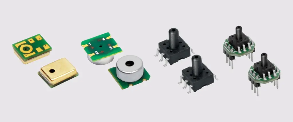
Air pressure sensors are devices used to measure and monitor air or gas pressure in a wide range of applications. They utilize different sensing principles to quantify pressure and convert it into an electrical signal that can be measured.
Types of air pressure sensors
There are various types of sensors used for measuring air and gas pressures. The common ones are:
Piezoresistive pressure sensors
Uses piezoresistive material that changes resistance when deformed
Very high precision, fast response, range up to 10 bar
How piezoresistive pressure sensors work?
Piezoresistive pressure sensors are one of the most commonly used types for measuring air and gas pressures. Below is an explanation of their working principle and construction:
Construction
Uses a diaphragm made of silicon substrate with piezoresistive elements diffused into it.
The diaphragm is etched to a required thickness to give desired sensitivity.
Piezoresistors connected as a Wheatstone bridge to sense resistance change.
Sealed reference vacuum chamber below diaphragm.
Working principle
Applied pressure deflects the diaphragm and introduces stress in piezoresistors
The stress causes change in resistivity of the piezoresistive material based on the piezoresistive effect.
This resistance change unbalances the Wheatstone bridge circuit.
The output voltage from the bridge provides a measure of the applied pressure.
Silicon provides excellent sensitivity, linearity and hysteresis characteristics.
Can detect pressure variations in the range of a few mbar up to 300 bars.
Signal conditioning
The output from the Wheatstone bridge is small and requires amplification.
Temperature compensation is added to cancel temperature induced resistance changes.
Additional linearization can improve measurement accuracy.
Provides standard voltage or current output proportional to pressure.
How capacitive pressure sensors work?
Capacitive pressure sensors use capacitance change to measure applied pressure. Their working principle is:
Construction
Contains two parallel conducting plates with air/dielectric between them.
Flexible diaphragm plate moves with applied pressure.
Fixed reference plate remains stationary.
Plates separated by small distance to allow movement.
Working principle
Pressure deforms diaphragm changing distance between plates.
This changes the capacitance between the plates based on formula:C = (εA)/d
Where,
Copy code
C = Capacitance ε = Dielectric constant A = Overlapping area d = Distance between plates
C is inversely proportional to d. So increase in pressure reduces d, increasing capacitance.
The change in capacitance is converted to equivalent voltage output.
Provides very high resolution and sensitivity. Range up to 100 bar pressure.
Temperature compensation required to account for thermal expansion effects.
How strain gauge pressure sensors work?
Strain gauge pressure sensors use the piezoresistive effect to measure pressure induced strain on the diaphragm.
Construction
Contains a pressure sensitive diaphragm with strain gauges in a Wheatstone bridge configuration.
Strain gauges attached to the diaphragm experience deformation proportional to applied pressure.
Change in strain gauge resistance unbalances the Wheatstone bridge.
Working principle
Applied pressure deforms the sensing diaphragm.
The deformation causes the attached strain gauges to elongate.
Elongation changes the resistance of the strain gauge proportional to the pressure induced strain.
This resistance change produces an unbalanced output from the Wheatstone bridge.
The output voltage is amplified and calibrated to indicate the pressure.
Provides very good accuracy and stability. Measures up to 500 bar pressure range.
Temperature compensation required as strain gauges are sensitive to temperature.
How piezoelectric pressure sensors work?
Piezoelectric pressure sensors utilize the piezoelectric effect to produce a voltage output proportional to applied pressure.
Construction
Sensor contains a piezoelectric sensing element sandwiched between two electrodes.
The element is usually made of quartz crystals structured to enhance the piezoelectric effect.
When mechanical stress applied to the element, the molecular structure generates charge.
Working principle
Applied pressure deforms/stresses the piezoelectric sensing element.
The mechanical deformation of the crystalline structure generates electrical charge proportional to the applied force.
The charge accumulation produces a voltage difference across the electrodes.
This voltage signal is conditioned and calibrated to provide the pressure measurement.
Provides very fast dynamic response to pressure changes.
Measures up to 300 bar pressure range.
Sensitive to temperature changes which affects output.
How optical pressure sensors work?
Optical pressure sensors use light intensity changes to measure pressure variations. Some common techniques used are:
Optical interferometry sensors
Uses a pressure sensitive diaphragm forming one mirror of a Fabry-Perot interferometer.
Applied pressure deforms the diaphragm changing the optical cavity length.
This alters the interferometry pattern of reflected light.
Photodetector measures the intensity changes which corresponds to pressure variation.
Fiber Bragg grating sensors
Uses fiber Bragg grating (FBG) sensitive to strain induced by pressure on diaphragm.
Pressure deforms diaphragm changing the grating period of FBG.
This shifts the reflected optical wavelength detected by an interrogator.
Wavelength shift indicates the applied pressure.
Provides very high resolution, fast response and electrical isolation.
Limited to lower pressure range up to 10 bar.
Key performance parameters
Some important specifications and parameters to consider for an air pressure sensor:
Pressure range – Minimum and maximum pressures that can be measured.
Accuracy – Maximum deviation between measured and actual pressure.
Repeatability – Ability to consistently return the same output for same pressure.
Resolution – Smallest change in pressure that can be detected.
Response time – Time required to reach a certain percentage of fullscale output.
Operating temperature – Temperature range over which sensor can function.
Thermal effects – Degree of output drift with changes in temperature.
Sensitivity – Ratio of output signal change to the input pressure change.
Nonlinearity – Maximum deviation from output linearity over full scale.
Hysteresis – Maximum difference between output readings for same pressure approached with increasing and decreasing pressure.
Overload capacity – Maximum pressure beyond full scale that can be applied without permanent damage.
Common applications of air pressure sensors
Some major application areas utilizing air/gas pressure sensors include:
Weather monitoring
Barometers for air pressure measurement
Altimeters for altitude based on air pressure changes
Weather stations forecasting system
Process industry
Measuring pressure in pipelines, vessels, reactors
Level, flow measurements using differential pressure
We are in an era where technology is taking over the world, from the education industry to hospitals and government. The application areas of tech grow each day with each advancement, making our life easier and less strenuous. However, these advances cannot happen without utilizing efficient equipment to work with. We are talking about PCBs, measuring equipment, processors, etc. This article will focus on the best printed circuits boards in the market, the TSM-DS3b PCBs. We shall answer questions such as “why is the Taconic TSM-DS3b PCB the best PCB in the market?” And what are the benefits of using this PCB? Hence to get the answer to this and more questions, stick around as we unravel the Taconic TSM-DS3b PCB mystery.
A Quick Overview of PCB
PCB is a coated sandwich structure of insulating and conductive layers. PCBs have 2 complementary functions:
Affixing electronic components into specifically designated areas on the outside layer through soldering.
Providing electrical connections between components’ terminals in a pretty controlled manner. Primarily known as PCB design, this connection should be reliable.
The Taconic TSM-DS3b PCB is a minimal loss core, thermally stable PCB. One can develop the Taconic TSM-DS3b PCB with the consistency and predictability of the most efficient epoxies reinforced with fiberglass.
Taconic TSM-DS3b PCBs are ceramic-filled and reinforced to ensure maximum efficiency. As per fiberglass content, these PCBs have tiny amounts of it, totaling up to ~5%. With these low levels of fiberglass content, the Taconic TSM-DS3b becomes pretty competitive in the market. That is because they rival epoxies as per fabricating large complex multilayers.
Taconic TSM-DS3b PCBs are good for the high power (thermal conductivity of 0.6 W/M*K) applications. In this case, the dielectric material must efficiently conduct heat being produced away from the other heat-producing sources. To do so, it utilizes a design known as PWB.
Taconic TSM-DS3b PCB was also invented to have pretty low coefficients as per thermal expansion in demand for thermal cycling.
As per microwave application, low z, y, and x values ensure that the critical spacings are between traces located in couplers and filters and have minimal movement with the temperature. What’s more Taconic TSM-DS3b PCBs utilize pretty low levels of profile foil copper. Hence they have copper edges that are pretty smooth in between the coupled lines.
Suppose you are looking for incredibly low dielectric losses, you can easily get at epoxy fabrication temperatures of 4500F. Combining the Taconic TSM-DS3b with a fastrise prepreg could be your answer. The FastRise-Taconic TSM-DS3b collaboration is an industrial leading solution with regard to low dielectric losses.
FastRise Prepreg
We utilize Fastrise prepreg in conjunction with various coating cores. The collaboration has resulted to the development of boards that have multiple layers for the ATE/digital/RF markets. When utilized in a board design that is symmetrical, Prepreg results in pretty optimum mechanical and electrical performance. Due to the bonding agent thermoset properties, it is possible to achieve multiple cycles of bonding with minimal delamination worry. Such efficiency merged with the Taconic TSM-DS3b bring out PCBs that have optimum performance.
What are the Benefits of Applying the Taconic TSM-DS3b PCB?
Utilizing Taconic TSM-DS3b PCB come with the following benefits:
The Taconic TSM-DS3b PCB has got the industry’s best DF. It has a DF of 0.0011 at 10GHz
High thermal conduction
Pretty low fiber content, as low as ~5%
Dimensional stability which rivals epoxy
Enables high layer large-format count PWBs
Builds rather complex PWBs, which yields predictability and consistency
Pretty stable temperatures DK negative thirty to positive 1200C
Resistive foils compatibility
What are the Applications of a Taconic TSM-DS3b PCB?
Store in an area that has minimal contamination properties
FastRise prepreg life shelf varies according to the following set conditions:
Refrigeration – refrigeration temperature should be 400F or lower
Room temperature – room temperature should be 230C or below plus a relative humidity of less than 50%
When you eject a FastRise prepreg from a refrigerator, let it accumulate heat till it hits room temperature while still in its sealed bag. In doing so, you reduce the possibility of moisture condensing on the FastRise prepreg. It also offers a consistent temperature as per the lamination process. When not being used, the bags should be sealed.
Shelf-life
When condition one above is observed, the FastRise prepreg has a 180 days shelf life after shipment.
When you observe condition two above, a 90 days shelf life applies for the FastRise after shipment.
Packages indicate the second condition by default, but the first condition has a longer shelf life.
PTFE are pretty stable chemically and electrically. Some of the reasons that make PTFE superior is in terms of performance over temperature and frequency. Also makes pure resins relatively soft. Due to this reason, Taconic overlays are glass fabric reinforced. The substratum reinforcement via glass fabric increases the X and Y axis stability. It hence overtakes the stability of the non-enforced PTFE products. However, even with this reinforcement, you still have to take some handling and process precautions. They help prevent deformation and damaging of the overlay during fabrication.
No Mechanical Scrubbing
As with flexible surfactant or thin cores, mechanical scrubbing stretches and deforms the material. We use pinch rollers to hold the panels in place during scrubbing leave dents. The brush accouterments are pressed onto the overlay surface. Instead of mechanical scrubbing, we would highly suggest that you try utilizing chemical cleaning.
When you eliminate unnecessary handling and mechanical cleaning, dimensional accuracy ultimately increases.
Avoid Picking up Panels Horizontally via One Edge or End
When you let the equipment flop over then you may end up stretching the substratum and copper. Hence you should instead pick the panels via two edges parallel to each other. Preferably you should utilize the two edges closest to each other dimensionally.
Prevent the Deposit of Contaminants on the Copper or Gear
Utilizing slip sheets and protective gloves that are clean prevents staining and contamination. If you do not deposit fingerprints, grease, and oils, you will not have to strain trying to remove them.
Avoid Mechanically Abrading PTFE Surfaces after Etching.
When not disturbed, PTFE surfaces are pretty good for:
After copper removal, there are rough tooth structures left behind, which make the PTFE surface pretty wettable. In case the surface is disturbed. Then more surface preparation via sodium etching might improve adhesion and wettability of the surface.
Avoid Stacking Panels onto each other Directly
When you stack up the panels, then debris or particles on one panel might leave marks on the surface of an adjacent panel. Hence instead of stacking them up, you should instead rack them up vertically. If you are looking to stack the panels up, then use a slip sheet that is soft and clean in between the panels. Also, ensure that the stack is of minimal height.
FastRise
Prepreg is usually supplied in between 2 release sheets. FastRise surface part might be tacky. You will realize that it is mostly recommended to let the prepregs accumulate heat before you open the bag. But it might be beneficial to utilize the FastRise while still cool in some scenarios which ultimately reduces tackiness.
Never let condensation form on a prepreg.
Preparation of the Inner Layer
Acclimation
There are cases where the overlay could be exposed to extreme temperature when being shipped or stored. It is important to place it in an ambient environment for 8 to 24 hours before processing.
Scaling
After copper foil etching, all overlays experience movement. There are such factors like:
The thickness of the copper foil
Circuit design
Glass style
Overlay thickness
All affect the dimensional stability of a Taconic TSM-DS3b PCB.
Lamination
Thieving/flow patterns
Copper borders that are solid and bear interlocking flow patterns, for example:
Honeycombs
Offset diamonds, are ideal.
Other patterns inhibiting resin-like flow patterns are also pretty ideal.
Do not utilize interlocking flow patterns. Also avoid patterns that promote resin-like flow patterns.
Conformance material and padding
We recommend press padding. Utilization of conformance material, for example:
Taconic tacPad
Clutch overlays
PTFE skive films or others
All these help in terms of balancing pressure variations through induction from circuits.
Pressure
You achieve full pressure before FastRise reaches 1200C. The resin flow of fastRise is proportional to the overlay pressure. Using pressure, one can control flow whereby high flowing prepreg part numbers act as slow-flowing or no flowing part numbers. Using this characteristic, one can achieve additional flow.
Conclusion
Taconic TSM-DS3b PCBs are pretty efficient. They have functionalities that add up to make it the best PCB on the market in the 21st century. We hope that this article has helped solve any questions you might have regarding the Taconic TSM-DS3b PCB.
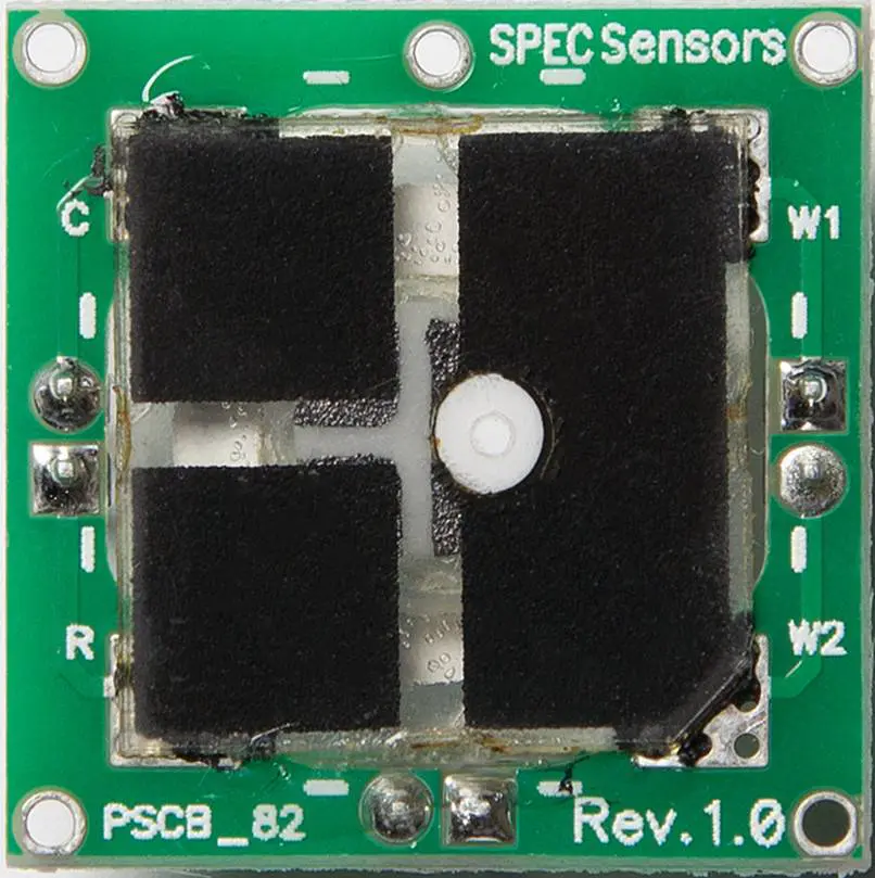
With climate change on the rise, air pollution has affected everyone. People have been trying to come up with ways to measure this phenomenon. Air quality sensors are critical for measuring and researching pollutants. These are pollutants that may be hazardous to public health and the environment.
Smaller, cheap, and satellite-based sensors with new capabilities have resulted from technological advancements. Ensuring the appropriate interpretation and quality of sensor data can be difficult.
Air quality sensors provide an estimate of particulate matter (PM). They can also measure gaseous pollutants in the air. It depends on measuring something unrelated to the actual pollutant. But, it is much easier to measure. For example, the sensor could measure the amount of light scattered by particulate matter. It increases as pollution levels rise. We sometimes present these results on a low, medium, and high scale. In the case of very basic air quality monitors such as smoke detectors, we present them on a binary scale.
What are air sensors
The term “air sensor” refers to a type of technology that has become more popular in recent years. It has the characteristics of reading a pollutant in the air and being smaller. They sell them at a price that allows for a more significant number of monitoring locations. RayMing PCB and Assembly use low-cost air, quality, and air sensor devices to describe this technology.
We have differences in the physical design of these technologies. They include monitoring air pollutants, managing data, and fueling the equipment. Some air sensors are usually used at a fixed location, while we mount others on vehicles or worn by the user. There are several variations in how these technologies get priced. The changes depend on whether the sensors get sold or leased. It also depends on maintaining and holding data from company to company.
One of the most serious risks to humans in modern society is air pollution. Poor air quality is to blame for so many of our ailments. That is why air quality measurement devices are essential for maintaining safety. Even if you can’t see the pollutants in the air, they are present and causing problems inside your body. It exacerbates health problems like asthma and can cause serious problems for people.
Individuals and families are better able to control their indoor air quality. But whether they take action to reduce their risk of pollution exposure indoors depends on how they perceive this risk. The awareness that risk is one of the essential prerequisites for this risk perception. Giving people personalized information about their risks impacts their attitudes and behaviors. So, research shows that people use experiential processes to understand risk. It also indicates that assisting people in experiencing risk may help them learn more about it.
What pollutants get measured by air sensors
Today, air sensors on the market measure a wide range of air contaminants, but not all of them. But, the main problem is if the air sensor will detect the target pollutant. This is in a combination of other pollutants and at the required concentration range for the application of interest. The EPA and outside parties focus their testing on real-world situations. They plan on expanding the number of air sensors that assess the six criterion pollutants controlled. They use National Ambient Air Quality Standards.
Consumer sensors can detect two basic forms of pollution. This is regardless of whether they are sensing inside or outside. They include:
1) particulate matter
2) gases.
There are many types of airborne pollutants. But these are the two that most consumer sensors can currently detect.
Particulate Matter
Particulate matter (PM) has both solid and liquid droplets. Some can be visible with the naked eye (for example, visible dust). At the same time, others need a microscope to view. PM10 and PM2.5 are the two principal size fractions of concern (size up to 2.5 micrometers).
The average human hair measures 70 micrometers in diameter. This is around 30 times the greatest diameter of PM2.5. The size of the object is crucial. PM2.5, for example, is small enough to enter the circulation after inhalation into the lungs.
Importance of Particulate Matters?
Health risks from airborne particles depend on their deposition in the respiratory system. The cilia, mucosa, and trachea work together to filter the thickest particles. They are about 5 mm in diameter. Particles with half to five millimeters can deposit in the bronchi. They can even get to the pulmonary alveoli. But they are quickly removed by the cilia of the bronchi and bronchioles. Particles with a diameter of fewer than 0.5 m can penetrate deep into the lungs and deposit in the alveoli.
Gases
Both outside and inside, several gaseous contaminants get discovered. For example, gases like nitrogen dioxide (NO2) and carbon monoxide (CO) get produced when we use fuel. It does not matter whether in a town industry, in your gas stove or furnace, or your car. These types of gases get found in your home.
Some portable sensors seek to measure volatile organic compounds (VOCs). They are airborne molecules, in addition to CO and NO2. You can find VOCs in household items’ off-gassing or cleaning sprays.
Categories of sensors:
– Gas sensors
– Dust monitors
– VOC (volatile organic compounds) sensors
– Ionizing radiation sensors.
A comprehensive sensor suite will include all these categories. In addition, different technologies allow for detecting hazards. These are that would otherwise go undetected at the same level. Some examples include high levels of radiation or substances with low toxicity. But they have high global warming (GW) power. We cannot detect the GW through infrared or chromatography technology.
Gas sensors
Gas sensors measure the concentration of gas in the air. We often use these sensors to measure indoor air quality and detect hazardous gases.
There are two basic types:
– Direct gas sensors measure specific gases. For instance, methane, ammonia, or carbon monoxide.
– Chemical gas sensors use chemical reactions to detect specific gases. For example hydrogen sulfide, or flammable gases, such as methane or propane.
Air quality sensors measure the concentrations of specific airborne substances. They include particulates (dust, smoke, pollen) and volatile organic compounds (VOC). Particulate sensors consist of a source (a fan), an optical system with a light source and detector. It passes through the particulate-laden air. The Electronics System performs digital signal processing on the detector signals.
VOC (volatile organic compounds) sensors
We detect VOCs by either infrared spectroscopy or gas chromatography. An important variant of VOC sensors is the VOC and carbon monoxide sensors. It detects specific hazardous gases in addition to VOCs.
Ionizing radiation sensors
Ionizing radiation sensors measure ionizing radiation (alpha, beta or gamma rays) or neutrons. We use ionizing radiation in nuclear reactors and nuclear weapons. But they can also occur naturally. The primary sources of this ionizing radiation are cosmic rays. They come from deep space and radon gas emitted by the earth’s crust. We process the data for further analysis after taking the measurements.
The range of different sensors used for air quality monitoring has grown over the years. In addition, companies are developing new technologies that detect lower radiation levels or different substances.
Air quality sensors detect gases such as ozone and particulate matter. Both are hazardous to human health and the environment. Governments work together to manage stationary air quality monitors that use sensors. These monitors are costly and need a supporting infrastructure. Officials use the resulting data to address pollution or issue air quality alerts.
A good example is the days with unhealthy ozone levels or during wildfires. These networks may overlook pollution at smaller scales and in rural areas. They don’t measure more localized pollutants that can cause long-term health effects. Some examples include ethylene oxide and toxic metals. Two advancements in sensor technology may aid in closing these gaps.
To begin with, we learn how low cost air quality sensor may now get used almost anyplace. They include fences, cars, drones, and clothing. People are now using these less expensive sensors. They use them to comprehend a variety of environmental and public health issues.
Second, for decades, agencies have been using satellites equipped with sensors. They track air quality to understand weather patterns and conduct research better. Recent satellite launches have sensors with improved air monitoring capabilities. The researchers use them in large-scale pollution investigations.
How does it work
To test air quality, low-cost sensors use various techniques. They include lasers. They estimate the size and number of particles passing through a chamber. We also have meters to estimate the amount of gas moving through the sensor. Most sensors use algorithms to turn raw data into usable readings. The temperature that affects sensor measurements is a factor in the algorithms. Humidity and other factors also. Other characteristics of higher-quality devices can improve findings. For example, adjusting the air temperature in the sensors provides consistent observations over time.
Satellite-based sensors track energy reflected or emitted in the atmosphere to identify pollutants. Some sensors track a single spot throughout time. At the same time, others track several portions of the globe.
To detect the creation, transport, and variability of pollutants and increase measurement reliability. Sensor installation in the network is essential. Combining data from several sensors can also improve their use. However, this raises the level of skill required to check the results. This is especially when the data comes from diverse sensors.
How mature is it?
Sensors have unique designs to perform specific tasks. They monitor the air within a building is now smaller and less expensive. As a result, they can now fill in gaps in monitoring and research in various ways. Local governments use wearable sensors to track different sources of air pollution. Scientists can use them to examine the exposure of research volunteers.
Low-cost sensors, on the other hand, have limits. They have fewer quality assurance systems in place than government-run sensors. The data they produce is of varying quality. It’s unclear how to install modern sensors or analyze the data to get the most value. Some low-cost sensors use artificial intelligence algorithms that the inventors cannot fully explain. This makes it challenging to comprehend variable sensor performance. Also, they frequently measure contaminants like ozone and particulate matter. There are hundreds of air toxins that could enjoy enhanced monitoring with sensors. But, there may be technological or other obstacles that make this impossible.
In the past, satellite-based sensors produced data infrequently and insufficiently detailed. So, newer sensors provide better data for monitoring air quality. It could help with rural monitoring and pollutant transportation, among other things. But, satellite-based sensor data might be challenging to interpret, particularly ground-level pollutants. Furthermore, current satellite-based sensor systems can only detect a limited number of pollutants. They include carbon monoxide, formaldehyde, nitrogen dioxide, sulfur dioxide, ozone, and particulate matter.
Comparison between different air sensors
Knowing which air quality sensor will work best with your Arduino/Raspberry Pi project is not easy. There are many different features and functions on the market. But, you won’t have to worry. You will learn various functions, applications, and accuracy of air quality sensors in the end. It will help you determine which one is best for your indoor project!
Air Quality Sensor Arduino
Have you ever wondered what’s in the air you breathe? Unfortunately, our cities are becoming increasingly polluted around the world. Air pollution is a silent killer that claims the lives of over 4 million people each year.
However, it is not only outdoor air that can be hazardous. When combined with poor ventilation, cooking can reduce indoor air quality. This is because burning fuels releases many tiny particles into the air.
Air quality sensors used to be expensive and difficult to obtain. We can now make our DIY air quality sensor Arduino in less than 15 minutes. One can use readily available microcontrollers like the Arduino and inexpensive DIY sensors.
Air Quality Monitoring
The methods for measuring air quality differ. It depends on whether you want to measure indoor or outdoor air quality.
Pollutants such as VOC, CO2, and dust can impact indoor air quality. We can get a good idea of indoor air quality by measuring one or more. However, for each of these pollutants, a different sensor’s required.
Pollutants from combustion engines are usually responsible for poor outdoor air quality. Fuel combustion produces tiny particles known as Particulate Matter (PM). These get classified according to their size.
The more dangerous the particles are, the smaller they are. For example, PM2.5 refers to particulate matter (PM) with a diameter of fewer than 2.5 micrometers in the atmosphere.
Long-term exposure to PM2.5 particles is hazardous to one’s health. The ability to measure your exposure to these harmful particles is crucial. In addition, it helps you to manage your exposure.
In this article, we’ll measure PM2.5 and its close cousins, PM1.0 and PM10.
The AQI is the most widely used metric for measuring. We also use it in comparing air quality levels in different cities worldwide.
This Arduino Air Quality Monitor gets used both indoors and outdoors. We use it to measure pollution from cooking, smoking, and other sources. Also, we can use it to monitor the air quality in your neighborhood.
A laser detects particulate matter in the most common air quality sensor for home that measures PM2.5. These laser-based sensors come in two varieties: those without a fan. For example, the Samyoung DSM501A and those with fans, such as the Plan tower PMS5003.
The fanless models are less expensive, but they are also less accurate. The Plantower PMS5003 is the best model at a reasonable price.
PMS5003 Air Quality Sensor
Particles are as small as 0.3 micrometers. Therefore, they can get detected by the Plantower PMS5003 sensor. This is why the sensor’s model number ends in ‘003’. The number 5 refers to the generation of the series.
On the back, you can see the air intake fan. This is what distinguishes this sensor from fanless designs like the Samyoung DSM501A.
The PMS5003 isn’t a current-generation model; instead, it’s the PMS7003. If you can find a more suitable deal on the PMS3003 or PMS7003 than the PMS5003, go for it. But, the Arduino code may differ slightly.
Working Principles
The PMS5003 scatters and radiates suspended particles in the air using a laser. The scattered light is then analyzed to produce a curve. It depicts how light scattering changes over time.
We then calculate the number of particles of various diameters per unit 0.1L volume of air by the sensor.
The PMS5003 is capable of producing the following:
· Concentrations of PM1.0, PM2.5, and PM10.0 in both standard and environmental units
· 10um, 5.0um, 2.5um, 1.0um, 0.5um, and 0.3um sizes of particulate matter per 0.1L air
Raspberry Pi air quality sensor
The Raspberry Pi is a cheap computing device created by an open-source foundation. It encourages the teaching of basic computer science in developing countries. The device became popular with makers who wanted an easy way to experiment with sensors and robotics. It created simple and miniaturized computers that fit on a single circuit board.
Since its inception, the Raspberry Pi has gone through four design iterations. It resulted in a larger format B model and a smaller Zero model. The Raspberry Pi’s appeal is that it is inexpensive and has a low entry barrier. If you can use a computer, you can use a Raspberry Pi.
The Raspberry Pi runs a Linux operating system. It includes networking, video, audio, and USB ports. This allows you to connect it to power, a screen, track, and keyboard. Also, you can write programs for it directly on the device!
Problems with Low-Cost Air Quality Sensors
The biggest issue with low-cost air quality measurement devices is the lack of data and accuracy they provide. These devices are notoriously inaccurate, and the information they provide isn’t always reliable. Measuring air quality is quite complicated. So opting for the highest-quality version is worthwhile.
You won’t tell the difference between each pollutant. This is mainly if you use low-cost air quality measurement equipment. You might find yourself in a situation where the meter says everything is fine. But the air contains a lot of ozone or other particulates. This is especially true for meters that can only measure a single type of contaminant. When this happens, it almost always leads to a health issue. It can cause you a lot of grief if people become ill due to attending your event. Low-cost quality measurement devices lack the technology required to provide accurate readings. The reading you need to aid in the fight against poor air quality.
Common challenges of using air sensors?
1. Air sensors may not be selective or sensitive for the target pollutant of interest. Real-world testing data can assist in determining whether a particular air sensor will produce data. This data should meet their application requirements.
2. Inaccurate readings result from low and high temperatures and excessive humidity levels. Air sensors may be imprecise, necessitating field calibration to get more precise data. Over time, many gas sensors become less sensitive to the target pollutant. This results in inaccurate readings. Some air sensors have a one- to two-year lifespan.
3. Not all air sensors are waterproof. Some air sensors need a physical enclosure to get protected from the elements.
4. Specific data communication technologies need air sensors, such as WiFi, cellphone, or Bluetooth.
5. It is possible that air sensors do not always collect data. Technology can fail, the power supply can run out, and weather can cause readings to get messed up. As a result, it’s critical to check sensors regularly to ensure they work correctly.
6. Performance. Low-cost sensors have a wide range of performance that is difficult to predict. Their algorithms may be opaque. Low-cost sensors used by various people may produce conflicting results.
7. Interpretation. Sensor data interpretation may need expertise. Sensors produce data in real-time that can be difficult to understand. They also don’t have short-term exposure health criteria. Many air sensors do not provide real-time data on a screen.
8. Management of information. Large amounts of data with inconsistent formatting get generated. This is due to increased monitoring, which will need to get stored and managed.
9. Alignment with requirements. Few low-cost, satellite-based sensors currently exist that can detect air toxics. Furthermore, low-income neighborhoods may have difficulties deploying low-cost sensors. These communities in studies are disproportionately afflicted by air pollution.
Testing The Air Quality in Your Home
Since home based air quality monitors have limits in their capabilities, you need good ones. If you care when it comes to air quality for home, we recommend measuring what’s in the outside air as the first step to undertake. You can do this using an outdoor-based air quality sensor. The outdoor conditions often determine indoor conditions. They measure only particle levels that are local airborne. They measure volatile organic compounds—gases such as cleaners, paint, and glue vapors. Radon and carbon monoxide, two fatal gases, are rarely measured. Numerous smoke detectors have the capability of detecting carbon monoxide.
Conclusion
Looking at the pollution, it is essential to have an air quality sensor in your home.
The technology we are using today is a product of CAD software. Many PCB design software come with high-quality. They are also customizable tools to help you create your next PCB. Many of my friends cannot even recognize what a PCB is and don’t know how it can be suitable for their lives. This article will go through some of the best free PCB design software out there.
If you want to design PCB, you need professional PCB design software to help you save time and money. Working with a good provider of software will save you time and money. You don’t have to look for an online translation tool to help you read some of the boards. You don’t have to spend time learning how to use the software either. When you have PCB design software, it does everything efficiently for you. Read on to understand what is PCB design software and which one will serve you best.
PCB design
You could ask yourself this question for those who want PCB design. What is a PCB? The PCB stands for a printed circuit board. It is a flat electronic component that has electronic components soldered and etched onto it. That is how a PCB works.
Alexander Bain introduced the early idea of the PCB in 1851. He created a board for Glasgow University that had both the electricity and data transmitted. It is a black slate-like component that has copper traces. The copper traces are where the electricity and data will go from one point to another.
The PCBs that we have today is helpful for many things. We can use them for telecommunications, electrical circuits, medical equipment, and automotive. It depends on the person designing the PCB who will be using it.
We can say that PCB is one of the essential inventions globally. It is changing the lives of humans everywhere. The creative technology for this product used CAD software that creates PCBs.
There are also plenty of other people looking to learn how to make a PCB. Finding the right road can sometimes be confusing. But you can always find the right step with your will and creativity.
The PCB design process is easy, but first, you must choose a PCB design software for your needs. That is the first step that you need to take if you want to start working on your PCB design in your life. The good thing about working with software is that it could help you create a PCB without issues.
1. Schematics PCB Design
This is the first thing you need to do to create your PCB. Creating an electronic schematic of your project is crucial in the process. You should do this stage carefully because it might have a bad PCB layout if you do not do it right. To help you with this task, many tools can help you create your PCB. Some are:
Inkscape is a popular program used to design posters, logos, and layouts on paper. One of the most used programs to create schematics from start to finish is Inkscape. Inkscape is free software that you can download on almost all platforms.
QElectroTech is another free program that can create schematics on PC and MAC computers. Users can only make printable PCB designs in QET using the STEP CAD files. It helps users with paper-free PCB layout design, layout, and library.
Altium Designer – If you are looking for paid software, you can opt for Altium Designer. This tool is good for beginners who want to start working with professional software. The price for this software is about $1500, which is cheap. In the long run, you will be getting many benefits from this software.
2. PCB layout Designing
You do this process next after the schematic designing part. It is not just drawing wires and writing stuff on the board here. You also need to think and plan before starting the layout design, which could take a while.
PCB Editor – This is a free and open-source PCB editor that we can use on Windows, Linux, and Mac OS. This software was initially developed in 1998 by one of the users of the Linux community. The development team has made several upgrades to this software since 1999. Now it is being maintained by a larger team of developers who produce new versions now and then.
KiCad is a total package tool for an electronic design. We can use it for schematic capture, PCB layout, and PCB production. It is well known for producing professional quality board layouts at an affordable price. It is free software that you can download from the internet.
Free PCBCart is a free web-based PCB layout tool. Users can create professionally designed boards online. Then they print them in China without worrying about shipping fees or import taxes. It is a convenient tool that users can create customized electronic boards online.
Steps:
a. Placing the component packages
Placing the component packages is also crucial in the PCB layout process. You will need to follow some specific steps to do this. They include Planarization, Bounding Box Creation, and the types of packages you will use.
Routing is the next process that you need to do if you want to produce a good PCB in the end. It is another critical step that you need to do carefully. You will need to use routing software for this process. Some good programs can do this job easily, such as:
Free Router is a free routing tool used on Windows, Linux, and Mac operating systems.
c. Vias
Vias is another essential thing you need to produce a good PCB. This process will involve drilling holes into the board to connect different tracks.
FreePCB is free and open-source software that can create PCBs on Windows and Linux operating systems.
d. Pad Selection
In this process, you need to select your pads as per requirement. You will need to make sure that you select the right width and diameter for the pads. Too thin of a pad will not be strong enough, while too thick of a pad will result in higher resistance and lower performance of your PCB.
PCBWay is the most popular online PCB fabrication service. People can order PCBs, assemble them, and get them shipped to their houses safely.
e. Exporting the layout design
The last step that you need to do is export the layout design. You should export your PCB design in a vector format later in other programs.
f. Manufacturing
After exporting your layout design, you will need to place your order on PCB fabrication services. You can place your order with Rayming PCB & Assembly to produce your PCBs and deliver them to your house.
Designing is not just drawing wires and writing stuff on the board. You also need to think and plan before starting the layout design. This could take a while. However, there are some steps that you can follow to make sure that you are doing it right.
The first thing you will need is to develop a proper design theme for your board. The theme should be good and attractive so that people will love it at first sight and want to buy your PCBs in the end.
1. Altium Designer
This is a paid PCB Layout software that can design circuit boards and create PCBs in general. It is the best in this area because it uses high-quality graphics. This software has codes for different PCB sizes and an excellent components library. It is a complete package tool that we can use for schematic capture, layout design, and fabrication of PCBs.
Features and specifications
Schematic capture
Layout design
PCB layout
Production of PCBs (in house and China)
Automatic documentation and documentation with notes
Online order status tracking and automated release of components. It allows production while keeping the design up to date.
Component libraries with over 100,000 components. They include many SMD components and surface mount parts
Auto capture of power traces, ground planes, and other essential trace characteristics
Electronic Design Automation – EDA (tools for schematic capture, PCB layout, and documentation)
A large library including libraries for BGA, SMT, and through-hole resistors.
An integrated system for developing with custom add-ons
Powerful libraries for optomechanical devices
A graphic library of hundreds of icons and symbols
This feature-rich PCB Layout software and used by more than 50,000 users worldwide. It is also considered the best in this area because it is easy to use, has many functions, and is very reliable in general.
However, it is a paid software that can cost you $2500 if you use all the features.
2. KiCad
KiCad is free and open-source software for creating PCBs or other electronic designs in general. It is a schematic capture, PCB layout, and electronic design automation software. We can also use it for producing matrices, schematics, and other PCB-related items.
It is free software that you can download from the internet. The software is user-friendly and is the most popular PCB design software.
It has a lot of functions that can help you design your PCBs. Therefore, many use it for its reliability and efficiency.
3. Eagle
Eagle is a powerful PCB Layout software used on Windows and Mac operating systems. It has a user-friendly interface that makes it easy to use by anyone who has basic computer literacy skills.
Unlike most other PCB design software, this tool is simple and easy to use for non-experts.
It has many features that we can use to create complex boards. They include unlimited board size and layers and a multi-sheet board design capability. It can use schematic capture with PCB layout on the same screen.
However, the free version of Eagle is not good enough. It only allows you to work in a small area and gives as many features as other tools.
4. gEDA
This toolkit is an integrated collection of tools for creating electronic circuits. It combines the four categories of tools needed for this task.
NASA also used it in its Space Shuttle in the beginning. We also use it to design other busses and GPUs.
The best thing about this tool is that it is free, open-source, and community-based.
We use it to create everything from simple schematic diagrams to complex PCBs.
However, it does not have many functions as you would see in Altium Designer.
5. ORCAD
This is another top-rated PCB design software. It can design and create various circuit boards. This software has the best features like parasitic extraction and 3D view. It is a total package design solution.
It also has a great library of components that we can use for creating your layout designs. You can find everything from resistors, test points to footprints for surface mount devices.
Universities and companies use it for professional purposes, making it one of the best options.
We can use it to create PCBs and schematics, layouts, and footprints. It also has rubber resistors, power distribution boards, and high-speed signal routing.
However, its free option is not good enough; therefore, you will have to purchase it if you use all the features.
6. Allegro
This is a tool for developing boards and systems and managing complex projects. It has different types of PCB layout capabilities, code generators. Also, it has a user-friendly interface making it easy to use by even those who do not have any experience in this area.
It has PCB diagrams, schematics, printed circuit boards, and an EDA flow. You can use it for single or double side PCB designs.
It can also design custom components and has a powerful library of parts.
However, this tool is not very user-friendly, and therefore, it is not the best option for beginners.
It is a relatively new tool and has many revolutionary features. We can use it to design PCBs.
It is easy to use and has an efficient layout tool with a snappy user interface for creating schematics and PCB layouts. It also has a library of components and components footprints. You can quickly create electronic circuit boards.
You can also generate professional documentation and reports using the built-in report generator.
However, this is still a relatively new tool. Therefore, there may be some bugs or issues you might encounter.
This is a free program that we can use to design, document, and share your projects. It is a user-friendly tool that is simple to use and has an easy library of components to use.
Fritzing has an intuitive interface and can create schematics, PCBs, and layouts.
It also gives an option of exporting designs into popular formats such as KiCAD. This makes it one of the best options for users just starting in this area.
However, it does not have a library of parts. Therefore, you can use a limited amount of components for your designs.
This is another software used to design various circuit boards and other electrical devices. It is an easy-to-operate software with an intuitive interface. This makes it very easy to use even by those new to the field.
The best thing about this tool is that you can use it free of charge and work with any board. This is one of the reasons why it has gained a lot of popularity.
You can also share your designs using the internal file sharing option. You can also use it for both single and double-sided designs.
It allows you to create schematics, PCBs, footprints, and printed circuit boards.
However, several bugs in this software may cause issues during the design process. If you are new to this area or have no experience, this software could be good enough for you to use, at least as a senior beginner.
10. Draftsight
This is a freeware program that Dassault Systemes launched in 2011. It has a user-friendly interface and is easy to use even for beginners.
This tool helps create both schematics and PCBs. It has different tools such as track, bus, component, net, and drawing tools that you can use to create your layouts.
It also allows you to view the 3D model of your design and also the component model, schematic, or PCB model.
What makes a good PCB design software?
You should consider several factors when choosing the best PCB software.
You should keep in mind and check out some things before finally choosing the one for yourself.
1. Price
The price of a PCB design software is an essential factor to consider. This is because there are several free options and paid ones that you can choose from.
A low-cost option could work for you, but it is best to go for paid software if you have a tight budget.
2. Database
The software’s type of database is another essential factor to look at. Some have databases that have all the necessary parts together. Others only have limited types of parts available with their packages.
Also, look at the size and quality of the database.
3. EDA flow
It is also good to check the version of EDA flow if you are purchasing or using this software for professional purposes. It is also a wise choice to first get an idea about which type will be best for your needs before choosing one in particular.
4. User-Friendliness
Check whether you can read the help provided by the software before purchasing. If it is user-friendly, then this is a good sign as it means that the developers have put in a lot of effort to make it easy to use for beginners.
5. Functionality
Apart from the factors mentioned above, you should check how well the software works for your needs and requirements. Run some demos and test-run your designs to see if there are any issues or bugs with them.
6. Library of Components
Another essential factor to consider is the software’s library of components. The more options it has, the better, as it means that you will find precisely what you are looking for.
7. Reputed Brand
Many brands provide PCB design software. Therefore, it cannot be easy to choose between them all. The best way to go about this is by checking out their popularity and reviews online and the number of users using their products.
8. Scalable
The software should also be scalable to allow the user to increase or decrease the size of designs. This is important as you may want to share your designs on the internet with others. Therefore, you need a program that allows you to do this.
9. Public Domain
Some better software like PCB CAD is helpful under the public domain. In this case, you can modify and redistribute it without paying anything for it. You will still get full rights (read: license) for its use.
There are several places where you can find free PCB design software.
The main places include:
1. Community forums
This is a great place to start looking for free PCB design software. However, you need to be very cautious before using such software. Many out there are not free but still, have some of their source code available for download. Therefore, this is not a good sign for safety purposes.
2. Web search engines
Another option that you can look at is a web search engine. Searching for ‘free PCB design software will pull up different results. However, you need to be very careful as many of these are scams and, therefore, are not a good idea.
3. Free Software Archives
This is another place to find PCB design software free of charge that the developer maintains. However, this is not very reliable as many users have reported problems with most of the programs listed in their forums sections.
4. Free Software Library
This is an excellent place to find free PCB design software that you can use for personal or educational purposes. However, this software may have limitations that could limit the number of boards and layers and the design’s size.
Conclusion
There is a lot to consider when choosing the best PCB design software. Depending on your requirements, purpose, and budget, you will choose one of the options mentioned above. The above guide is a good starting point for finding the best software for your needs. Try the demos and test the functionality of each before purchasing or downloading them to have a better idea about them. You may also want to check out other helpful resources like this course. Good luck!
Do you hate those long walks you have to take to switch off the lights at home while you go to bed? Well, you are not alone on that part. The good thing is that we are in an era whereby this tedious task is now easier via sound sensors. Now you can turn your lights on and off by just clapping your hands. You can play cool games in real life with your friends and do amazing things that did not seem possible a while ago via this technology. But how do sound sensors work? How can clapping your hands signal your lights to turn on or off? Well, in this article, we shall dive into these questions and try to answer them in the best possible way. We shall look at things such as:
Sound sensors are a great wonder; when well understood, you can create pretty fascinating projects. Hence without further ado, let us help you put together the sound sensor puzzle.
Sound Sensor
What is a Sound Sensor?
We define a sound sensor as a module that detects sound waves via the sound’s intensity and then converts it to electric signals.
Sound sensors function like our ears, having a diaphragm that converts vibrations into signals. However, since the sound sensor is not human, it does not have an actual diaphragm or actual ears. A sound sensor instead consists of a peak detector, an amplifier (LM393, LM386, et cetera) that is highly sensitive to sound, and an inbuilt capacitive microphone. Sound sensors, having these components, can function correctly. They follow the following process to “hear” sound:
Sound waves are propagated through air molecules.
The sound waves are received by the inbuilt capacitive microphone
The sound waves are then amplified and digitized for the processing of sound intensity
Through this process, sound sensors can detect when you clap your hands to switch on the light or when you want to switch them off. Of course, to achieve this feat, you will have to go the extra mile but worry not because we have got you on that.
Applications of a Sound Sensor
Other than being useful alongside with Arduino to build incredible projects (we shall get into this later on), sound sensors can also be essential in so many day-to-day applications which include:
Monitoring and security systems such as door alarms, burglar alarms, et cetera.
Sound level recognition and ambient sound recognition
Home automation, for example, lighting your house by clapping or even whistling instead of having to manually turn off the lights via a switch
These applications are pretty fascinating and aim at making our lives easier. With the great tech advances taking place, you are bound to see this list get longer and longer as sound sensor application areas grow.
To understand the concept of a sound sensor, let us look at an interface sound sensor using Arduino.
Arduino Sound Sensor
If you are looking to add the concept of sound to your next project, then this section might help you out a lot. In this section, we shall look at:
How a sound sensor’s microphone works
The sound sensor’s board interface
How to merge a sound sensor onto an Arduino board
How does a Sound Sensor’s Microphone Work?
Have you ever used a microphone before? If you have, you might have been puzzled about how you speak into it using a low tone, and the sound gets amplified as it gets outputted via a speaker. To know how this works, we have to get inside of a microphone, not literally, of course! But by reviewing every part of a microphone, this is because sound sensors utilize the same features, only that the sound sensor microphone is pretty tiny.
Inside a microphone, you will find a thin diaphragm that is actually one capacitor plate. You will also find another plate known as the backplate. The backplate is parallel to and close to the diaphragm. When sound waves hit the microphone, the diaphragm vibrates. The diaphragms vibration causes a change in capacitance as the plates either get farther apart or closer together. The change in capacitance causes voltage change across the two plates, which, when measured, can be useful in determining the amplitude of the sound.
Now that that is out of the way, we can now look at the sound sensor’s board interface.
Sound Sensor Board Interface
A sound sensor is actually a tiny board that brings together a microphone (50Hz – 10KHz) and processing circuitry, which converts sound waves to electrical signals. A sound sensor board has three crucial parts, namely:
Electric signals are fed onto the high-precision comparator found on the sound sensor’s board for digitization. The signal is then made available at the OUT pin.
To take things up a notch, you can set up a threshold using a potentiometer found on the sound sensor’s board. Using this threshold, you get to learn when the amplitude of sound is HIGH (in this case, it exceeds the threshold) or when it is LOW (lower than the set threshold). Using this setup, you can set an action to be performed once on reaching a certain threshold. For example, once you clap your hands, this sound wave can cross the set threshold, which in turn will trigger the switching on of light (the action). You can play around with this setup to generate so many cool projects.
The sound sensor interface also has two LEDs, one for power and the other for status:
The power LED – lights up on powering up of the module
The status LED – it lights up when the digital output goes LOW
Sound Sensor Pinout
A sounds sensor has only three pins:
VCC pin – it supplies power to the sound sensor. It’s recommended to power your sound sensor with a voltage between 3.3V and 5V.
GND – A ground connection
OUT – acts as the sounds sensor’s output. It outputs high whenever conditions are quiet and LOW whenever there is detection of sound. You can connect the OUT pin to any digital pin on an Arduino board or onto a 5V relay directly or a similar device.
To properly utilize the sound sensors utilities, you can hook it up to an Arduino board to develop a sound sensor Arduino; let us see how this is possible.
Connecting a sound sensor onto an Arduino board is relatively simple. It would help if you started by connecting the VCC pin on the sound sensor module to 5V on an Arduino board, then connecting the GND pin to the ground. Now plug in the OUT pin to the digital pin on your Arduino, and that’s it, you have mounted a sound sensor onto an Arduino.
Sound Sensor Calibration
To attain accurate readings from your sound sensor, you should calibrate it. Sound sensor modules come with a built-in potentiometer useful in calibrating the digital output (OUT).
To calibrate your sound sensor, all you have to do is adjust the potentiometer until you attain your desired threshold. Start clapping near the sound sensor’s microphone as you adjust the potentiometer until you see the status LED blink responding to your clap. Remember that the set threshold determines what the digital output will output. Once you exceed the threshold, it outputs LOW. Hence the wrong calibration can mess up your entire project.
Once you have calibrated your sound sensor, you can now utilize it with no accuracy worries for your project.
How to make Sound Sensor Devices
Now that you have successfully mounted a sound sensor onto your Arduino board and you have calibrated the sound sensor, it is about time we see what this combination can do.
The following example simply detects claps or snaps then prints a message on the serial monitor; all you have to do is connect your Arduino to a computer and type in this program:
#define sensor in 7
Unsigned long lastEvent = 0; // variable that stores the time at which the last event happened
Void setup(){
PinMode(sensorPin, INPUT); // sets sensor pin as an INPUT
Serial.begin(9600);
}
Void loop(){
int sensorData = digitalRead(sensorPin); // reads the sound sensor
if (sensorData == LOW) { //if the sensor pin hits LOW, sound is ultimately detected
if (milli () – lastEvent > 25{ //if 25 milliseconds pass since the last detected sound,
//it means that the clap is detected and not because of any spurious sounds.
Serial.println(“clap detected”);
}
LastEvent = millis(); // remembers when the last event occurred
}
}
If everything is functioning fine, the Arduino should detect sound once you clap and display “clap detected” on the serial monitor. You can play along with this program adding in new functionalities until you develop a pretty cool project.
Troubleshooting
If you detect that the sound sensor is misbehaving, try out the following steps to fix it:
Double-check the power supply to ensure it is clean. Because sound sensors utilize an analog circuit, they are more prone to power supply noise.
The electric microphone utilized on a sound sensor is pretty sensitive to wind noise and mechanical vibration. It would be best if you hence mounted it with a resilient material. Doing so can help absorb vibrations.
The sound sensor’s sensing range is pretty small, probably around 10 inches. It would be best to clap your hands or make a noise near the sensor’s microphone to attain a better response.
That is how you can make a sound sensor. It is pretty straightforward, but you can use it for a lot of things that range from:
Clap switches
UV light meter
Room lights that utilize sound sensors
Adding sound wave properties to your project has never been that easy.
Now that we know how sound sensors work, let us take things up a notch by looking at some advancements made in sound sensors:
The NXT Sound Sensor
Have you ever heard of the NXT sound sensor before? Do you know how this sound sensor functions? Well, if you do not have answers to both or even one of these two questions, then this section is for you. We shall go through the NXT sound sensor and the incredible new features that it brings to the table. Hence follow along!
The NXT sound sensor is a sound sensor that comes in two different variations:
The normal sound sensor
The ultrasonic sound sensor
How does the NXT Sound Sensor Work?
The NXT sound sensor functions like a standard sound sensor mounted onto an Arduino board but with some advancements that make it unique. Due to these advancements, robots can utilize NXT sound sensors to “see” and detect objects as they move around.
The NXT sound sensor detects both DB (decibels) and DBA (adjusted decibel).
Decibel – We measuresound pressure in decibels.
DBA – in detecting DBA, the sensor’s sensitivity is adapted to the human ear’s sensitivity. These are sounds that you can hear via your ears in simpler terms.
DB – detects unadjusted (standard) decibels; this means that this sensor can detect sounds that are too low or too high for the human ear to hear.
The NXT sound sensor can detect and measure sound pressure levels of up to 90DB – that is almost equal to the sound pressure of a lawnmower. Sound pressure levels can be extremely complicated. Hence most NXT sound sensors display reading in percentages. The higher the percentage, the higher the sound being detected. For example:
4% to 5% is like a quiet living room
5% to 10% is like a person speaking from a distance
10% to 30% is like the noise generated when you are conversing with a person at close range
30% – 100% is like the noise produced by people shouting or when you are playing loud music
The Ultrasonic Sensor
Robots utilize the ultrasonic sensor for “vision” and detection; using this sound sensor, robots can sense and measure distance, detect movement and avoid obstacles. But how can sound sensors help in all this? Well, that all lies in the mystery known as the ultrasonic sensor.
Ultrasonic sensors utilize the same scientific principle that bats use. It produces a sound wave and then measures the time taken to hit an obstacle and then bounce back, the same way you hear an echo, only that the sound wave they produce is not as loud. Huge obstacles having a hard surface return the best reading. Curved obstacles (like a ball) made of soft fabric, or small in size are pretty hard to read for the sound sensor.
You should also note that two or more ultrasonic sensors working in the same room tend to interrupt each other.
Phasmophobia
Games are a major branch of tech. I mean, in the 21st century, almost every handset gadget comes with a game pre-installed. What’s more, games are evolving whereby we now have virtual reality games that you can play and experience everything as if you were literally in the game console yourself. Others utilize infrared, sound, and motion sensors to create a gaming environment out of your normal house. One of these incredible games the phasmophobia.
Phasmophobia is a horror game that utilizes sensors to detect a “ghost” in a room designated for the game. These set sensors are unlocked once you hit level seven through level eight. Once unlocked, you can utilize these sensors to record readings from the ghost. For the sensors to work, you have to place them on walls. Once you have perfectly placed the sound and the motion sensors, you can move back to your truck and monitor them.
Phasmophobia Sound Sensor
People use sound sensors to detect any movement that might occur in any of the designated rooms. To use the sound sensor, equip it onto your hand and then stand near a wall; you will see a hologram. Choose the most appropriate place to mount your sound sensor and you are good to go.
A sound sensor will detect any movement activity in the entire room. To visualize the radius of your sound sensor, head on to your truck and check on the map where you mounted the sound sensor. The sound sensor’s radius will be displayed in yellow giving a clear visual of the radius.
Remember that the sound sensors, once mounted on a wall, picks up any movement that occurs in the room. Therefore, if any of your teammates wander into a room, the sound detector will sense them and produce a false alarm. When the sound sensor picks up sound, it displays an alert on the gaming monitor. The room that has the sound sensor will also be displayed on the monitor.
When used with infrared and motion sensors, sound sensors give phasmophobia a great touch that makes the game super thrilling. Now that is what we call taking things up a notch.
Phasmophobia Motion Sensors
Phasmophobia motion sensors function exactly like sound sensors but have a pretty small radius. Therefore the best place to mount your motion sensor would be in an alley. Alleys have a straight line detection range, making motion detection pretty easy.
When a motion detector senses motion, it displays an alert on the map’s screen in the truck. Motion sensors cannot differentiate between a teammate and a ghost too.
Now that we are in the motion sensor section let us look at motion sensors with sound.
For security purposes – this is the core use of motion detectors
How do Motion Sensors with Sound help as per Security?
If anyone comes into your house while you are away, you will want to know about it since they might be thieves. Well, motion sensors with sound will alert you immediately they sense movement in your house while you are away. To avoid false alarms, you have to activate these motion sensors when you want to use them and deactivate them when you don’t.
How do Motion Sensors with Sound Function?
Motion sensors with sound work pretty much like sound detectors. See, when you are moving around, you send out vibrations. A motion detector picks these vibrations via a diaphragm, just like the sound sensor’s, and then wave conversion occurs. While playing a game such as phasmophobia, the instance anything or anyone sends out a vibration (might be vibrations from footsteps), the motion sensor with sound picks up this vibration and produces a reading.
Ultrasonic Motion Sensors
An ultrasonic motion sensor is another motion sensor that utilizes sound to detect motion. Ultrasonic motion sensors utilize the same principle that is used by microwave sensors. However, ultrasonic motion sensors use sound waves instead of bouncing off microwaves on obstacles. By bouncing off sound waves on surfaces, these motion sensors can detect motion and produce readings.
Sound Sensor Projects
Before we wrap things up, let us leave you with some sound sensor projects that you can try out on your own to test the knowledge that you have gained from this article:
Sound pollution detection
Using a sound sensor, you can develop a device that can sense overall sound and air quality. In doing so, you can help reduce sound pollution in your area.
Baby monitor
You know how babies can cry for hours and hours when no one is around. That can be a problem, but one that can be solved using a sound sensor. A baby monitor that utilizes sound sensors can pick up noise and alert you when the baby starts to cry. You can add more features, such as a camera, to increase the monitor’s efficiency.
Dog barking tracker
Dogs tend to sometimes misbehave when left home alone. However, using a dog barking tracker, you can easily track your dog’s barking to know what your dog is up to. Of course, you will have to first track the dog’s barking pattern, but after that, you are good to go.
These are but a few of the many projects you can develop using a sound sensor.
Conclusion
A sound sensor is a crucial device that can do wonders in the tech industry. Its applications are endless, and benefits seem to go up every day. We hope this article has answered all the questions you might have heard regarding sound sensors and their application.
The RF-30 is one of the most advanced synths available, but it has one shortcoming: there is no digital control interface to speak of. The builder must get a digital control interface to use the instrument’s many functions. The availability of the RF-30 software development kit (SDK) and other documentation makes it possible to create an entirely digital interface using a small embedded microcontroller. This document describes this solution and its development process.
For more than 35 years, Taconic has delivered innovative products. These products have safely protected hundreds of thousands of high-value components. Taconic’s product line includes many enclosures, from hard-plastic cases to foam-injected molded cases. As a result, Taconic can develop the ideal enclosure to protect your component. It can also meet your performance requirements by working with customers.
One should install the PCB before mounting any modules (since all the available slots are helpful in the base and side panels). To install it, use one or two M4 21mm screws (depending on the size of RF-30 PCB). These screws must pass through corresponding holes from both sides of the case. Place them into mounting holes at around 2.5” (60mm) from the rear of the case. This will ensure that the screws do not interfere with any components on the opposite side of the PCB and will work with any TL-30 or RF-30 case.
We can use the RF-30 PCB as a stand-alone product. However, it was originally designed to interface with a microcontroller. Therefore, it helps provide digital control and interaction. The Taconic SDK provides complete C++ code for programming an Atmel AT90S2313 microcontroller.
There are three types of enclosures available: the RF-30, TL-30, and MM-30. The RF-30 is the largest in the line, measuring 11.8” (w) × 6” (h) × 2.5” (d). On the other hand, the TL-30 and MM-30 are both 7.5” (w) × 7.5” (d) with space for an 8-pin DIL package, allowing for quick and easy installation and removal of the components.
The RF-30, TL-30, and MM-30 cases are available in various materials. They include plastic, aluminum, fiberglass, ABS plastic, and steel. For more information on Taconic product materials, see the “Material Guide.”
The RF-30, TL-30, and MM-30 are all based on the same design. The enclosures comprise three main modules: the base and the lid, which form a hinge, and two specialized modules on the sides. Each module has 4 or 5 pins (A, B, C, and D).
Design procedure
We mount the base to a metal plate using eight screws that pass through holes in the metal plate to secure it to the case. Then, we secure the lid to the base using two screws that pass through mounting holes in the base and the lid.
Each module accepts four additional screws, one in each corner. The four small holes in each corner secure a mounting bracket with a DIL socket; plugging it into one of these DIL sockets will power the module. Although you could mount this bracket inside the case, we do not recommend it since it may interfere with access to signal pins on other modules.
There are three optional modules on the sides, bringing the number of available mounting points on a case up to six.
The design of the RF-30 PCB allows mounting on top of the modular side modules. To mount it, you must remove two sets of screws at the rear of the case (marked with a *) and then slide two tabs into slots on either side.
Next, extend each tab fully and press into place one panel beside the other. This will secure the PCB to the case and slid in place when one fully extends the tabs.
Benefits of using Taconic RF-30 PCB
There are many advantages to using a Taconic RF-30 PCB as an interface to the RF-30:
The RF-30 PCB’s design is for direct use with the RF-30. It does not require any additional components and does not expand on the capabilities of the base module or the lid. Instead, it adds a digital interface for the user, greatly expanding the capabilities of this exciting synthesizer and focusing its potential on audio making.
1. Low cost
We can use the RF-30 PCB design with the RF-30 for cost reasons. It does not require additional components or expand the capabilities of the base module or the lid. It adds a digital interface for the user, greatly expanding the capabilities of this exciting synthesizer and focusing its potential on audio making.
2. No proprietary or application-specific hardware
The RF-30 PCB has no proprietary parts. As a result, it is very highly hackable. So, we can use it for many other applications and do not limit the application of the RF-30 PCB in any way. Many of these applications are possible. This is because of the extensive documentation and codebase provided with the Taconic SDK.
3. Excellent peel strength
Its design is essential in working with the RF-30. It can withstand extreme shock, vibration, and temperature conditions.
IF DESIRED, we can use the RF-30 PCB in place of the lid. It has extra connectors that run along the length of the PCB. The RF-30 PCB has a design to connect to pots, switches, LEDs, or any other peripheral that requires just a few connections. It does not have to have a DIL socket (it also doesn’t need one as an interface).
4. Exceptionally low DF
The digital construction makes it easy to design low-cost PCBs with short traces and high DF. These characteristics enable us to use the PCB in many situations that would be impractical for conventional PCBs (such as breadboards) or difficult for standard PCB kits (such as in conjunction with LCDs, real-time clock chips, etc.).
5. Excellent intermodulation performance
Because of the design’s digital nature, performance is excellent for a product of this price point. The ability to run the PCB at ±5V also allows us to use it with high-level signals.
The RF-30 PCB will interface with any microcontroller that supports I2C and SPI communication. They include Atmel and Freescale microcontrollers. The RF-30 PCB design is essential for direct use with the RF-30. So, it does not require any additional components and does not expand on the capabilities of the base module or the lid. It adds a digital interface for the user, greatly expanding the capabilities of this exciting synthesizer and focusing its potential on audio making.
6. Low moisture absorption
Because the PCB consists of high-quality components, it is water-resistant and dust-proof. This is important as several RF-30 modules and accessories generate electrically-conductive dust that can cause electrical problems if it builds up in the system.
7. Enhanced surface smoothness
Unlike some surface-mount components, these parts are not rough on the top side. This allows us to use the PCBs on many surfaces that would destroy conventional PCBs.
Taconic RF-30 PCBs are explicitly designed for the RF-30 and are incompatible with any other synthesizer. Therefore, you must purchase the following components from Taconic Instruments:
You cannot purchase the PCB individually. A kit is available, including all parts, a set of cases, and a PC board. Building a single unit requires 20 minutes, while building several may take significantly longer. It is possible to build more than one unit simultaneously. Additionally, even an inexperienced builder should complete the assembly in just a few hours.
The RF-30 PCB design allows you to use it with the RF-30 directly. It does not require any additional components and does not expand on the capabilities of the base module or the lid. It adds a digital interface for the user, greatly expanding the capabilities of this exciting synthesizer and focusing its potential on audio making. 9. Optional LED matrix
The RF-30 is an exciting synthesizer with many applications. One of the nice things about the Taconic SDK is that it provides code to support all these applications:
1. Base station Antennas
Leading PCB manufacturers such as RayMing PCB and Assembly create the RF-30 PCB for direct use with the RF-30. It does not require any additional components and does not expand on the capabilities of the base module or the lid. It adds a digital interface for the user, greatly expanding the capabilities of this exciting synthesizer and focusing its potential on audio making.
2. Home automation
It provides a complete means of controlling your Atmel microcontroller-based systems, including door locks, temperature control, etc. It can control up to 64 Atmel 328P and 328Px based modules.
3. LCDs
The RF-30 has several analog input pins that we may use to drive LCDs. We should connect these pins to the appropriate I2C address.
4. Extra functionality
The RF-30 PCB has extra connectors that run along the length of the PCB. Additionally, their design allows for connecting to pots, switches, LEDs, or any other peripheral that requires just a few connections. It does not have to have a DIL socket (it also doesn’t need one as an interface).
5. Inventor’s Kit (IK) serial port connection
This provides an inexpensive means of connecting the RF-30 to control software on an attached PC. As a result, any software user will have a complete means of creating new modules, applications, and effects.
6. PWM or frequency modulation (FM)
The RF-30 has analog inputs that we can use for PWM or FM. We can connect these inputs to the appropriate I2C addresses.
7. Temperature control and remote control
Since the RF-30 PCB design allows for direct use with the RF-30, it does not require any additional components and does not expand on the capabilities of the base module or the lid.
Conclusion
The Taconic RF-30 PCB has a unique design to work directly with the RF-30. It does not expand the capabilities of the base module or the lid. Instead, it adds a digital interface for the user, greatly expanding the capabilities of this exciting synthesizer and focusing its potential on audio making. In addition, the price is low, and it accepts standard packages of components such as DIL sockets, potentiometers, and LEDs. It is an excellent addition to any RF-30 system for cost and performance.