How to Analysis PCB If Circuit Board Failure

ENEPIG pcb

Introduction

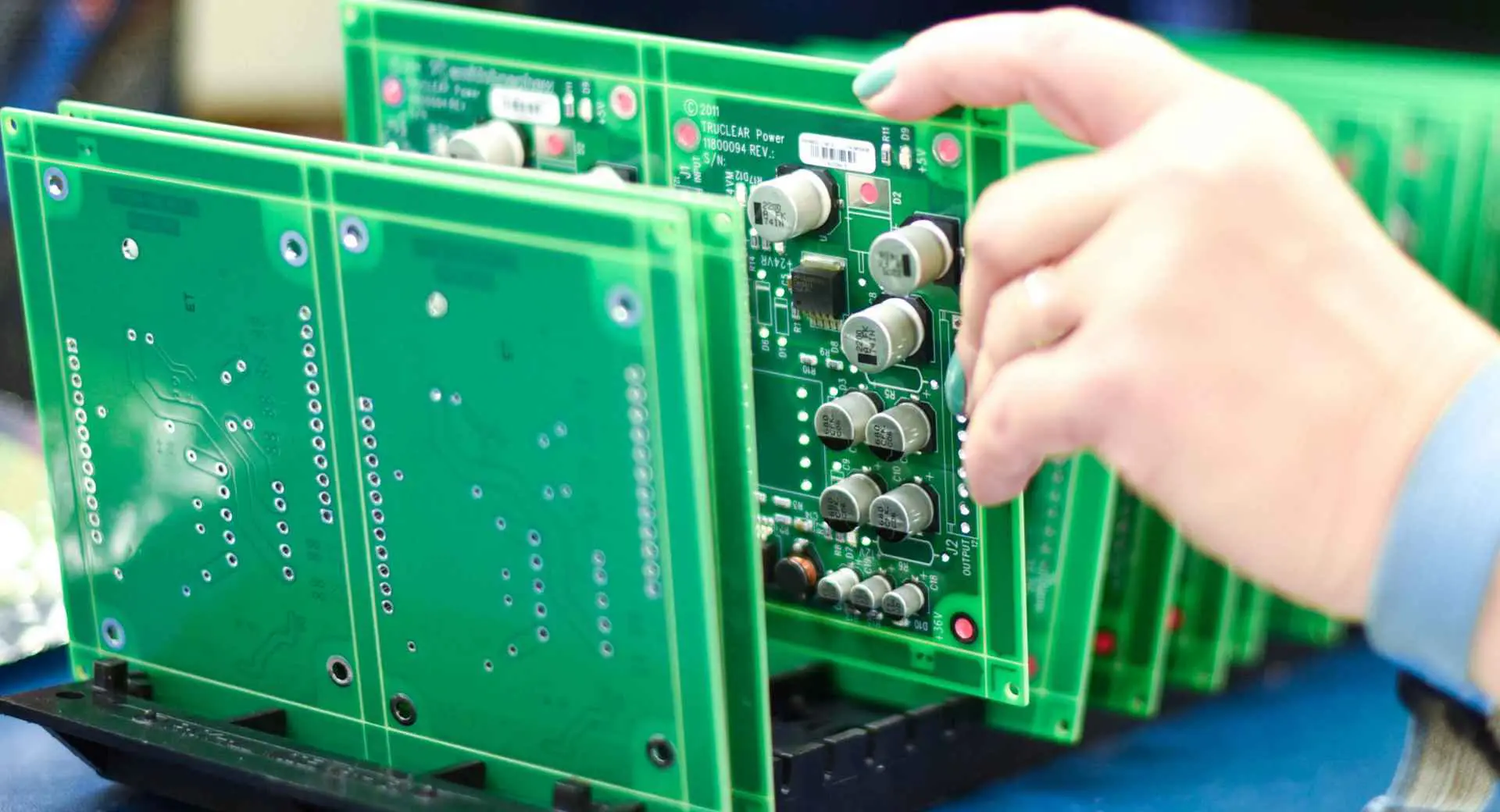
Despite best efforts during design and manufacturing, printed circuit board (PCB) failures still occur in electronics products. When boards fail prematurely or pass testing but then fail in the field, systematically analyzing the PCBs is key to identifying root causes so corrective actions can be taken.

This article provides a comprehensive guide on processes for analyzing failed PCBs including:

  • Signs indicating PCB failure modes
  • Tools for inspecting boards non-destructively
  • Techniques for performing failure analysis
  • Methods for isolating and capturing faults
  • Failure analysis lab capabilities
  • Examples of common PCB failure mechanisms
  • Steps for performing root cause investigation
  • Documentation and reporting on analysis results
  • Implementing corrective actions

By leveraging rigorous PCB failure analysis procedures, companies can improve product reliability, reduce associated costs, and strengthen customer satisfaction.

Signs of PCB Failure

What Are the Common Factors That Cause PCB Circuit Board Failure

Prior to detailed analysis, certain signs indicate likely printed circuit board issues:

Field Failures

  • Performance degrades or functionality stops after a period of use
  • Suggests failure mechanisms like:
    • Thermal cycling fatigue
    • Corrosion
    • Contamination
    • Signal or power integrity issues

Testing Escapes

  • Units pass manufacturing test but fail in the field
  • Indicates:
    • Incomplete test coverage
    • Faults triggered only under certain use conditions
    • Intermittent or latent defects

Manufacturing Defects

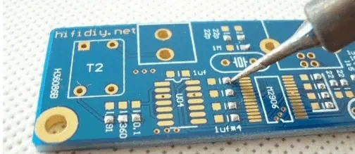
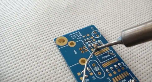
  • Failures during production testing
  • Caused by defects like:
    • Soldering errors
    • Contamination
    • Assembly errors
    • Handling damage

Thorough failure analysis then confirms failure modes and pinpoints root causes.

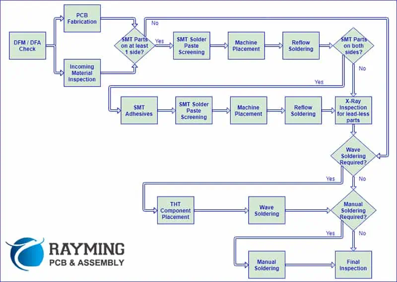
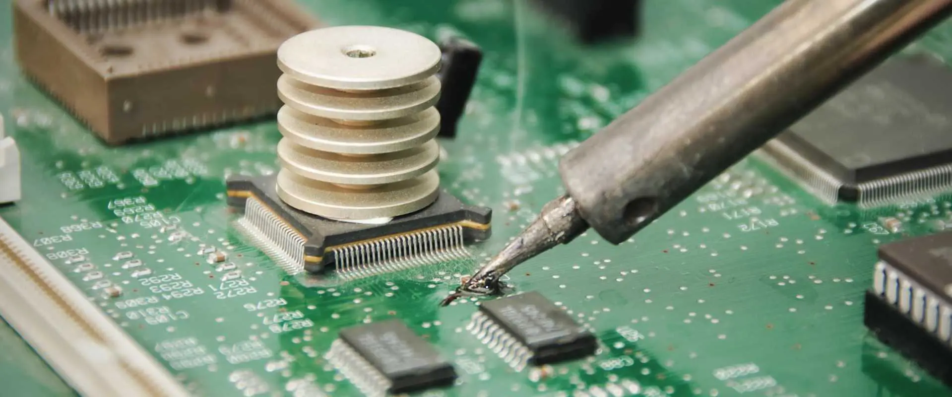
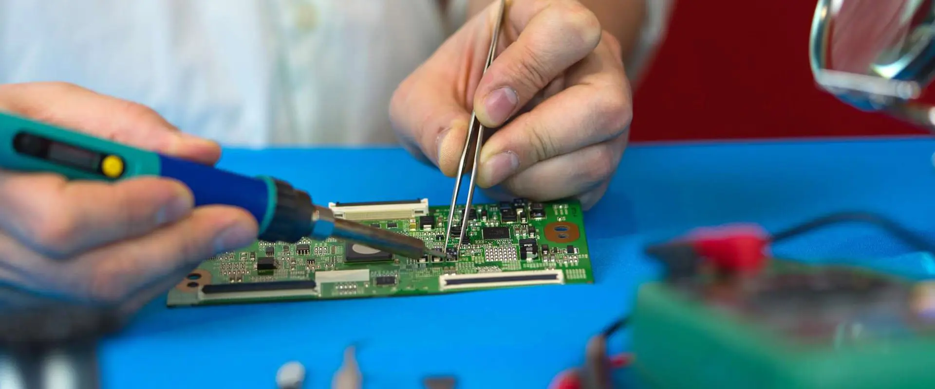
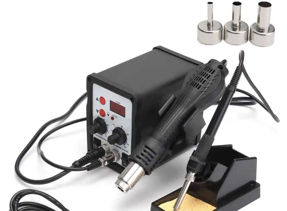
Tools for Inspecting PCBs

Several tools allow non-destructive inspection of boards:
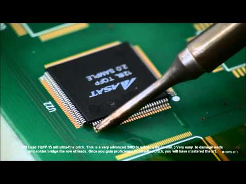
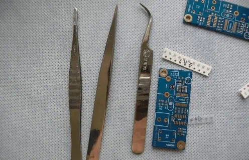
Visual Inspection

  • High magnification inspection microscopes
  • Reveal component damage, contaminants, discoloration

X-Ray Imaging

  • See inside components and PCB structure
  • Requires only simple sample preparation

Automatic Optical Inspection (AOI)

  • Imaging systems scan board features
  • Detect missing or malformed components and solder

Boundary Scan Tests

  • Leverage on-board test structures
  • Verify interconnect integrity and basic device functionality

Quick screening using these tools guides more detailed analysis on probable fault locations.

Techniques for Failure Analysis

To isolate causes after identifying suspect regions, several laboratory techniques are employed:

Electrical Testing

  • Probe stations perform in-circuit tests on nodes
  • Functional testers exercise system behavior

Signal Integrity Analysis

  • Oscilloscopes probe waveforms and signal integrity
  • Time and frequency domain analysis

Emission Microscopy

  • Captures infrared emission from operating board
  • Hot spots indicate elevated resistance

Thermal Profiling

  • Scan surface temperatures under operating power
  • Find hot components suggesting power or thermal issues

Chemical Analysis

  • Chemical stripping followed by microscopy
  • Reveals buried traces and vias with defects

Cross-Sectioning

  • Cutting through defect area
  • Inspect thinly-sliced cross section under microscope

Electron Microscopy

  • SEM provides high-resolution images of traces and solder
  • EDX detects contaminants down to ppm level

These proven techniques isolate faults and determine the physics of failure.

Methods for Capturing Intermittent Faults

Capturing transient or intermittent faults presents challenges:

Temperature Cycling

  • Rapidly heat and cool board
  • May trigger temperature sensitive failures

Vibration Testing

  • Subject board to shaking across a spectrum of frequencies and amplitudes
  • Can precipitate latent mechanical failures
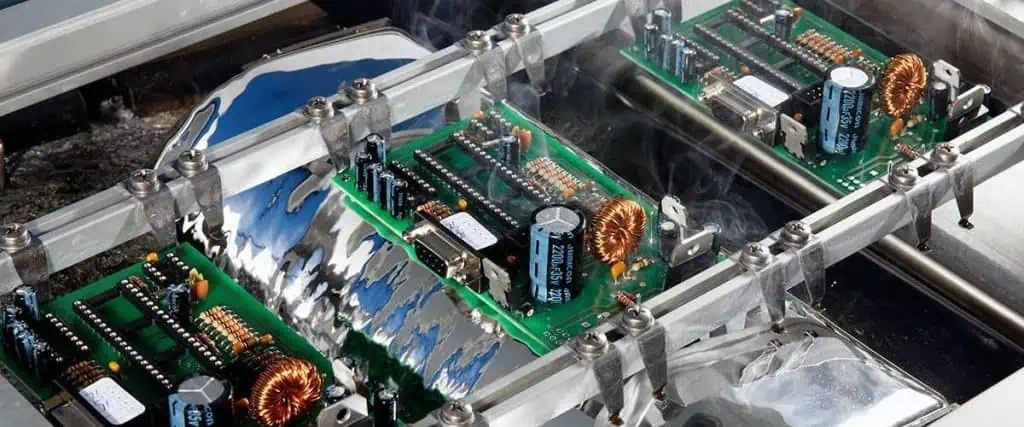
Accelerated Aging

  • Apply excess voltage and temperature over time
  • Encourages early manifestation of latent defects

Signal Monitoring

  • Logic analyzers or oscilloscopes monitor nodes
  • Capture glitches suggesting loose contacts or noise

With persistent testing modifying conditions, transient issues can be observed, isolated, and analyzed.

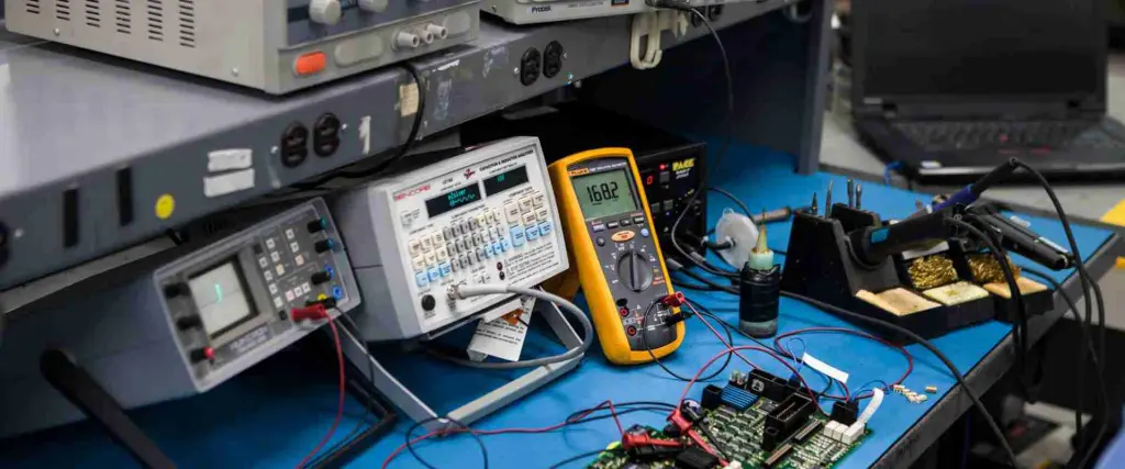
Failure Analysis Lab Capabilities

Dedicated failure analysis labs boast extensive capabilities to investigate complex faults, including:

  • Electrical probing stations
  • Emission microscopy systems
  • Temperature forcing chambers
  • X-ray imaging tools
  • Focused ion beam circuit editing
  • Scanning electron microscopes
  • Transmission electron microscopes
  • Vibration testing systems
  • Nanoprobing and picoprobing
  • Sample decapsulation and cross-sectioning
  • Advanced chemical analysis tools

Experienced technicians leverage this array of equipment to uncover failure mechanisms.

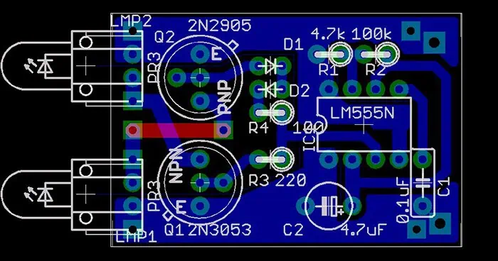
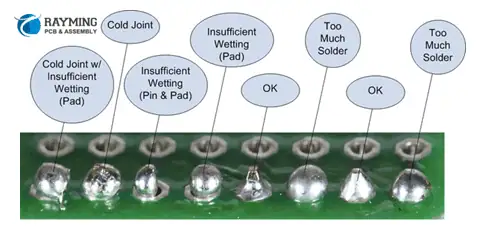
Common PCB Failure Mechanisms

During analysis, many common failure causes may be discovered:

Thermal Cycling Issues

Contamination

  • Conductive debris shorting traces
  • Corrosion from flux residue or environmental agents

Manufacturing Defects

  • Solder bridging
  • Missing or reversed components
  • Plating voids in vias

Power Integrity

  • Unacceptable voltage drops under load
  • Ripple or noise disrupting circuits

Signal Integrity

  • Uncontrolled impedance causing reflections
  • Crosstalk or ground bounce exceeding margins

EMI/EMC Problems

  • Radiated interference above acceptable limits
  • Susceptibility to external fields disrupting operation

Awareness of these and other common mechanisms guides investigation.

Performing Root Cause Analysis

To identify underlying root causes rather than just physical defects, a rigorous process is followed:

Replicate and Monitor Failure

  • Trigger failure modes discovered earlier
  • Use tools like emission microscopes to watch propagation

Map Sequence of Events

  • Construct timeline of effects culminating in failure
  • Look for initiating sources and chains of secondary effects

Evaluate Design Margins

  • Review stress models and margins of safety
  • Narrow down weak points with inadequate guard band

Assess Manufacturing Variability

  • Characterize typical distribution of assembly variations
  • Failures often trace back to outliers

Reconstruct with Physics-of-Failure

  • Develop hypothesis using established failure models
  • Check against sequence of events and forensic evidence

Identify Process Gaps

  • Look for shortcomings in design rules, modeling, parts selection, assembly processes that allowed defect
  • Strengthen weak links in development chain

The root cause may have origins across design, manufacturing, parts, testing, field conditions or other domains.

Documenting and Reporting Findings

How to repair Lifted Pad on PCB

Clear documentation and reporting ensures knowledge is retained and findings are actionable:

  • Document analysis details in lab notebook
  • Photograph defects from multiple angles before and after manipulation
  • Record microscope imagery and measurements
  • Note test configurations and procedures
  • Organize findings and supporting evidence in report
  • Summarize key conclusions and priorities for corrective action
  • Present to stakeholders and solicit feedback

Complete records aid root cause validation and process improvements.

Implementing Corrective Actions

Failure analysis is ultimately only valuable if it spurs needed improvements such as:

Improved Design Practices

  • Tightened design rules
  • Expanded modeling
  • Wider safety margins

Material and Parts Changes

  • Higher grade substrates
  • Screening or derating components
  • Change at-risk materials

Manufacturing Process Refinements

  • Tighter process controls
  • Improved operator training
  • New test coverage
  • Tools maintenance and calibration

Product Specification Modifications

  • Relaxed operating temperature range
  • Lower derated voltages
  • Additional shielding

Customer Guidance

  • Installation or operation guidelines
  • Handling and storage recommendations
  • Periodic maintenance advice

By driving changes, failure analysis efficacies company processes and products.

Frequently Asked Questions

Here are some common questions about PCB failure analysis:

Q: What tools allow non-destructive inspection of boards?

Optical inspection, x-ray imaging, automatic optical inspection, and boundary scan tests are common techniques.

Q: How can latent intermittent failures be identified?

Methods like temperature cycling, vibration testing, and burn-in can precipitate failures under accelerated conditions.

Q: What types of chemical stripping expose buried traces and vias?

Chemical etchants like nitric acid or ferric chloride preferentially attack copper allowing inspection of underlying features.

Q: When would emission microscopy be used over thermal profiling?

Emission microscopy offers higher spatial resolution useful for small components, but thermal profiling allows observation of the entire board.

Q: How long does a comprehensive failure analysis usually take?

From initial electrical test, fault isolation, physical analysis, and root causing, 1-2 weeks depending on complexity.

Conclusion

Rigorous failure analysis is crucial for improving product reliability, customer satisfaction, and ultimately the company bottom line. While a systematic investigative process requires investments in tools, training and technician time, the dividends include reduced costs from returns and enhanced process excellence across the product lifecycle. By leveraging the guidelines described here when boards fail, engineers can elevate the maturity of designs, manufacturing methods, and quality standards.

How Are Double Sided SMD Boards Assembled? Full Process and Comparison

pcb vs pcba

turkey PCBA

We make thousands of boards every week, we know whatโ€™s involved in the prototype pcb assembly of all types of boards. So if youโ€™re considering a board for your projects, we thought weโ€™d share an overview of the production process and considerations with you in advance.

YouTube video

If youโ€™re unsure about any particular part of the process then certainly get in touch with us. Otherwise, we hope the following outline helps improve your understanding of how double sided SMD boards are assembled.

How are double sided SMD boards assembled? Itโ€™s very simple. First, assemble and solder one side and then, flip it over to do the other side. When the solder paste is applied to the other side the melting point needs to be a bit lower. So it doesnโ€™t affect the flip side. Then it needs to be run through pick-n-place and vapour phase soldering again.

The Difference Between Single and Double Sided Assembly Boards?

Both these PCBs are widely used in different types of electronics. Starting with computers, smartphones, radio controls to other everyday consumer electronics, PCBs are an integral part of the electronic equipment we use in our everyday lives. However, single and double-sided PCBs have different uses and are manufactured a bit differently as well.

Single side PCB are part of many different types of electronics while double-sided PCBs are generally used in more advanced technologies. Depending on the need, output and cost, manufacturers choose the type of PCB.

Single-sided PCBs usually has conductive metal and components mounted on only one side of the board. Conductive wiring, generally of copper, is used to connect through the other side. Double-sided PCBs are a bit more complex. They have electronic components mounted on two sides and the wiring crosses over both sides. It is difficult to produce but its uses outweigh the cons and the labour-intensive process.

double side PCBA

PCB Assembly and Manufacturing Process

There are various stages that form part of the assembly and pcb manufacturing process. The solder paste needs to be applied, then the components will be placed onto the board, then soldering, review and testing. All these steps are carefully performed to ensure the best possible quality in the final product. Hereโ€™s more information on what each step entails:

Solder Paste

This is the first step of the pcb assembly process. This paste needs to be applied to those sections of the board which will be soldered. Generally, these are the component pads. The solder paste is a mixture of small grains of solder and flux. This can be deposited into a particular location using a process similar to the printing process.

Then a solder screen is used to place it directly on the board and at the correct position. A runner pushes across the screen ejaculating small amounts of paste on to the board. Since the screen is generated from the PCB files, it has holes in exactly the same locations as the component pads on the boards.

Pick and Place

Next, is the pick and place. It is referred to as a machine that helps put the components together with the board. Once the board with the solder paste is ready, it is run through the machine. The machine already has the components loaded into it. It will use dispensers to position the components in their respective area on the board.

The components will be held together due to the tension of the solder paste. In some assembly process, small dots of glue are also used. However, that is a practice usually reserved for wave soldered boards. Practicality suggests that using glue makes any kind of repair work difficult. However, some glues are made to degrade during the soldering process.

Soldering

Now that the paste is added and components have been placed on the board, itโ€™s time to get them soldered. This is done by passing them through the soldering machine. Some boards are also passed through a wave soldering machine in this part of the process, but that is not widely used in surface mount assembly. The solder paste is given a miss when wave pcb soldering is used. Reflow soldering is more common than wave soldering in contemporary manufacturing.

Review

This step is also known as inspection. After the boards have been soldered, they are inspected. For surface mounted assemblies, it is not possible to perform a manual inspection. The automatic optical inspection is more practical in this regard. Machines generally inspect the boards to detect joints, component placements and if the right components have been placed.

Testing

After the inspection, the boards are tested to ensure that theyโ€™re in proper working condition. As a result, theyโ€™re tested in numerous ways. Thereโ€™s a wide range of instruments used to test the boards including an analogue multimeter, oscilloscope, digital multimeter (DMM), frequency counter, pulse generator, etc.

Feedback

Finally, to ensure that the entire process remains true, the feedback from the current batch is reinstituted into the process. This helps keep the process and the components on track to ensure an efficient process.

The process is inspected to find errors and any failures detected during these steps are reinvestigated. The inspection stage is the ideal time for finding issues. As a result, defects can be detected rapidly and corrections reincorporated.

pcb-assembly-process-1

Manufacturing Difficulties and Risks

PCBs form the main backbone for the electronics that theyโ€™re incorporated in. As a result, when the board malfunctions, it affects the entire device. Thatโ€™s why weโ€™re constantly checking our production process to ensure we minimize any of the difficulties that many other PCB manufacturers struggle with.

Errors can also be due to regular wear and tear or manufacturing defects. But in the case of manufacturing defects – predominantly produced by less reputable sources, companies should be identifying the errors or gaps and address them. Here are a few of the most common issues faced in production if you don’t have the kind of quality control systems installed that we do.

Burnt Circuit Board

During the manufacturing and assembly process, the board is exposed to varying degrees of temperature. Some are very high. So high, that they can burn the board. Each component of the board has its own durability and breaking point. As a result, if thereโ€™s not enough space on the board, it might burn the board.

Poor Component Manufacturing Quality

Poor manufacturing quality is referred to as a variety of quality issues that happen during the assembly. Generally, issues such as connection troubles, bad solder or loose components.

Another risk if the proper care isnโ€™t taken during soldering is if thereโ€™s residual flux. Flux is used during soldering and can damage components if itโ€™s left behind on the board. When selecting a PCB manufacturer to work with you need to ensure they have quality control processes in place to mitigate against these issues, if in doubt, get in touch with us to ensure a quality checked board every time.

Effect on Costs

This has always been a question when it comes to manufacturing PCBs. Do we go with single sided or double sided boards? Which one costs less? However, answering that is easy. But the main question should be which one costs less for you.

Single sided boards pcb cost less invariably simply because thereโ€™s less to do. Double-sided boards fit more components and thereโ€™s two sides fitted with components and then soldered. As a result, itโ€™s obvious that double-sided boards will be more expensive.

However, what do you do when your needs are more acute towards a double-sided board and a single sided board just wonโ€™t do? Thatโ€™s why you need to consider which one costs less in your case. Cost management is an essential part of ensuring an efficient process. More errors or defects mean more wastage and more costs, especially since double-sided assembly is more tricky.

Cost Comparison

Itโ€™s difficult to compare the actual cost of the two boards without knowing the exact setup, so itโ€™s worth contacting us for a quote.

Both the boards are made up of the same material, same insulator and conductor. The main difference between the two is the conductor placement and thru-holes on each board.

However, there are three main categories which decide the costing – Primary, Secondary and Overhead. Hereโ€™s an overview of what components fall in each category:

Primary or Fixed Production CostsSecondary or Dependent CostsOverhead Costs
Board SizeToolingFacility
Number of PCBs produced in a production runLayout โ€“ trace design, hole size, and hole countLabor โ€“ salaries and benefits
Number of layers beyond double-sidedLaminationEquipment
Lead timeChange needed from mechanical drill type to laser drill typeRaw materials
Hose size and countQuality assuranceChemical processes
Material type and thicknessVia fillWastewater treatment
LayoutFabricationRegulatory permits
 FinishCost of delays due to design or fabrication changes

Advantages of Double Sided SMD Boards

There are two main advantages that a double-sided SMD board provides over a single sided board:

1. Since the board has two sides to mount components, there is a higher density of components. This means that the board can carry more components but without congesting the space since there are two sides. As a result, this makes the process of laying tracks easier.

2. The second advantage is that thereโ€™s increased heat dissipation due to the added layer of copper. During the etching process, the copper is removed to create tracks but then reinserted instead of leaving it out completely.


Common Uses for Double-Sided SMD Boards

Single-sided PCBs are generally used in a wide variety of electronics and applications, including camera systems, printers, radio equipment, calculators, and much more.

Similarly, double-sided PCB is also used in a wide spectrum of electronic products including lighting systems, vending machines, amplifiers, car dashboards, and many more.

PCB Assembly

Conclusion

In conclusion, both single sided and double sided are important – but in different applications. Their uses are different since both boards are built in different manners. Similarly, their costing is different due to the same reason. Based on the application, cost and other factors, a manufacturer can decide on a single sided or double sided board.

If youโ€™re not sure which board you need, then get in touch with us here at RayPCB and weโ€™ll be happy to talk through your requirements, provide the best method for your needs and ensure you get quality manufactured PCB boards.

What is SMT Footprint?

pcb footprint

Introduction

Surface mount technology (SMT) has become the predominant method of electronics assembly and component packaging, replacing older through-hole technology. In SMT, components are directly mounted onto the surface of printed circuit boards (PCBs) without passing leads through holes. The land pattern or pads on the PCB that connects the component is known as its โ€œfootprintโ€.

This article provides a comprehensive overview of SMT footprints encompassing pad geometries, sizes, mask openings, orientations, specialty pads and how footprint design accommodates components packaging and joining methods. Guidelines for optimizing and standardizing footprints are also discussed. By understanding SMT footprint design, PCB engineers can layout robust and manufacturable boards.

SMT Footprint Elements

A typical rectangular surface mount component is soldered onto the PCB through metallized terminals or leads on the underside. The corresponding SMT footprint consists of the following elements:

  • Pads: Copper pads connect each component terminal to a conductive trace on the board.
  • Soldermask openings: Expose the copper pads while covering other traces for solder control.
  • Silkscreen outline: Indicates component placement and orientation for assembly.
  • Text markings: Identify component designation, polarity etc.
  • Fiducials: Alignment markers for pick and place machines.

Pad Geometries

Footprint in PCB

Pads come in different shapes with dimensional attributes tailored to component needs:

  • Rectangular: Most common pad shape suited for perimeter leads.
  • Rounded rectangular: Rounded pad corners reduce stress concentration.
  • ** Oval**: Accommodates pitches down to 0201 sizes while allowing sufficient solder volume.
  • Square: Used for area-array packages like BGAs, CSPs etc.
  • Donut: Ring pad for shielding cans to allow visual solder inspection.

Key pad dimensions include length, width, corner radii, and finished copper thickness. Typical length/width ratios are 1:1 to 1:1.5. Rounded corners use 20-25 mil radii. Pad thickness aims for 1-2 oz finished copper.

Pad Sizes

Pad sizes primarily depend on three factors:

  1. Lead dimensions: Pad size should match component lead width and provide sufficient overlap for wetting and adhesion. Excessive extension beyond the lead is avoided.
  2. Solder volume: The pad must accommodate adequate solder to form a reliable joint. IPC-7351 guidelines provide minimum volumes based on lead sizes.
  3. Solder mask openings: Pads sizes account for registration tolerances by exceeding mask openings to avoid open circuits. A 25-50 ฮผm annular ring is typical.

High density components may use smaller pad sizes passing minimal solder current to maintain soldering yield across adjoining pads.

Soldermask Openings

The soldermask opening dimensions relative to pads control solder flow and bridging:

  • Width/Length: 25-100 ฮผm greater than pad ensures alignment tolerance. Too large increases bridging risk.
  • Shape: Match pad shape but enlarged evenly on all sides for uniform wetting.
  • Expansion: Can enlarge openings in high vibration areas prone to solder masking separation from pads.
  • Clearance: Minimum 50 ฮผm spacing from adjacent pads, or proportional to voltage difference.
  • Corners: Right-angled corners simplify masking process capability over rounded.

Orientation Markers

Footprints visually indicate component placement and orientation on the board using:

  • Silkscreen outline: Indicates footprint edges and aligns component body.
  • Polarity marker: Rectangles or triangles denote orientation of polarized components.
  • Text markings: Component designators and values marked adjacent to placement.
  • Fiducials: Crosshairs or circles designate pick-and-place locations.

Specialty Pad Types

Unique pad configurations are designed to accommodate different packages:

  • Castellated: Edge pad extensions bond to castellated leads of MEMS and LED packages.
  • Thermal: Exposed thermal pads provide enhanced thermal dissipation path from packages.
  • Metal core: Directly bonds components onto exposed metal core PCBs.
  • Compliant interface: Provides stress relief between rigid components like connectors and PCBs.
  • Gull wing: Formed pad recesses allow flush bonding of protruding gull wing leads.
  • Press fit: Plated through holes accept press fit pins for mounting connectors.

Standardized Footprints

elegantly arrange PCB silkscreen

PCB software libraries contain vast collections of manufacturer approved footprints for common components and packages. Standardized footprints enable:

  • Correct dimensions: Meets component requirements for reliable assembly.
  • Interchangeability: Allows substituting components from different vendors.
  • Design reuse: Eliminates reinventing footprints for repeated components.
  • Manufacturing compatibility: Provides compatible known-good footprints for fabrication.

However, non-standard custom footprints may still be needed for innovative package designs.

Footprint Design Guidelines

Strategies for optimizing SMT footprints include:

  • Match pad sizes to lead dimensions with sufficient tolerances. Avoid overly large pads.
  • Incorporate appropriate rounded corners and radii to reduce solder voiding.
  • Utilize polarized markers, fiducials and text for clear component orientation.
  • Expand solder mask openings beyond pads for solder release and bridging prevention.
  • Increase pad spacing in vibration-prone regions.
  • Thermally connect large pads to inner plane layers for heat dissipation.
  • Allow for rework and repair access in placement and routing.
  • Verify footprints against manufacturer recommendations and PCB standards.

Conclusion

Designing suitable SMT footprints requires expertise in combining pad geometries, soldermask openings, thermal considerations and assembly practices into an optimal layout matching the component. Standardization using verified footprints saves time while avoiding field issues. SMT will continue to evolve with components getting smaller, pads becoming denser and higher assembly precision requiring even better understanding of good footprint design principles by engineers.

Frequently Asked Questions (FQA)

Q1: What is the typical copper thickness used for surface mount pads?

A1: 1 oz (35 ฮผm) is suitable for most SMT pads. Higher current pads may use 2 oz (70 ฮผm) thickness. Electroless nickel-immersion gold (ENIG) plating provides solderability.

Q2: How are soldermask openings aligned to pads in actual PCB fabrication?

A2: Soldermasks are photo-imaged using the same copper pad images on the PCB layers to achieve self-aligned openings. This removes need for precise registration of separate soldermask layers.

Q3: Why should thermal pads be connected to inner plane layers?

A3: Connecting exposed thermal pads directly to internal ground or power planes allows heat conduction from components through vias into the planes for effective spreading and cooling.

Q4: What is the typical clearance between copper pads and neighboring soldermask openings?

A4: A minimum 50 ฮผm clearance is typical to avoid solder bridging between adjacent traces. Higher voltage differences require larger spacing proportional to voltage.

Q5: How does footprint design accommodate densely packed fine pitch ICs and components?

A5: Miniaturized pads, tighter spacing and pitch matching, smaller rounded corners, and thin soldermask expansion gaps enable mounting fine-pitch components. Laser direct imaging improves resolution.

Difference Between Cold welding and Pseudo Soldering

Soldering Circuit Boards

Introduction

Joining metal parts is critical in manufacturing across industries including electronics, automotive, aerospace, machinery and more. Soldering is the most common electrical interconnection method used to attach electronic components to printed circuit boards (PCBs). However, emerging direct solid-state joining techniques like cold welding and pseudo-soldering are gaining attention as lead-free solder alternatives.

This article provides an in-depth comparison between cold welding and pseudo-soldering processes encompassing the bonding mechanisms, joint microstructures, applicability for electronics assembly, processing considerations, joint strength and reliability. By understanding the capabilities and limitations of both methods, engineers can select the right approach for manufacturing robust metal-to-metal interconnects.

What is Cold Welding?

Cold welding refers to solid-state joining of metals well below their melting points by applying high pressures to create intimate contact between atomically clean surfaces. This allows interatomic bonding across the interface without fusion of the base metals or use of filler alloys.

The bond initially forms due to Van der Waals forces between surface atoms. Further plastic deformation under pressure breaks up surface films and contaminants enabling actual metallic bonds between the virgin parent metal lattices.

What is Pseudo-Soldering?

Pseudo-soldering produces solder-like intermetallic joints through solid-state interdiffusion between metal foils and substrates at temperatures below the bulk metal melting points. Specially formulated multi-layer composite foils are placed between parts and heated under pressure. Interdiffusion between the intermediate reactive layers and the substrates creates intermetallic phases that join the parts.

The intermetallics grow similar to transient liquid phase bonding in soldering, but without becoming molten. Hence the name pseudo-soldering. The intermetallic joint resembles solder in appearance and meets process requirements for electronics assembly.

Bonding Mechanisms Comparison

ParameterCold WeldingPseudo-Soldering
Bond FormationMetallic bonds between cleaned metal surface atomsInterdiffusion creates intermetallic phases
Base Metal StateRemains solidRemains solid
Intermediate PhasesNoneIntermetallic transient liquid phase
Pressure NeededHigh (25-100 MPa)Lower (3-10 MPa)
Bonding TemperatureAmbient to 300ยฐC180ยฐC to 350ยฐC
Surface Finish DependencyHighly dependentDepends on interlayer
Reactivity with MetalsLowHigh due to interlayers

Joint Microstructure Comparison

Cold Welded Interface

The interface preserves parent metal microstructures with minimal heat affected zones. Direct metallic bonds reform across the interface. Some trapped oxides or voids may remain.

Pseudo-soldered Interface

Intermetallic compounds form across the interface analogous to soldered joints. The intermetallic thickness depends on thermal exposure. Minimal heat affected zones are present.

Electronics Assembly Comparison

ParameterCold WeldingPseudo-Soldering
Process TemperaturesUp to 300ยฐC180ยฐC to 350ยฐC
Pressure NeededVery highModerate
Tooling ComplexityHighLow to moderate
Throughput SpeedSlowModerate
Surface SensitivityHighLow
Component MetallizationsLimited material compatibilityWide material compatibility
Defect SensitivityLowHigher voids, bridges
Design AdaptabilityRequires major redesignDrop-in solder alternative
Equipment InvestmentVery highModerate modifications

Bond Strength Comparison

Well bonded joints exhibit parent metal fracture strengths proving the interface is stronger than the base metals. Joint strengths over 200 MPa are easily achieved for many material combinations with both cold welding and pseudo-soldering.

However, actual bond strengths depend significantly on surface cleanliness, flatness, pressure consistency, metallurgical compatibility, and process parameter control. Defects like trapped oxides, voids, and poor interdiffusion lower bonding strength and reliability.

Reliability Considerations

Cold Welded Joints

  • Prone to stress corrosion cracking along trapped oxide zones
  • Subject to fatigue failure under thermal cycling due to high elastic modulus mismatch across interface
  • Hermetic seals can be achieved

Pseudo-soldered Joints

  • Intermetallic compounds may suffer thermal fatigue and brittle failure
  • Interdiffusion quality affects electromigration resistance
  • Lower hermeticity due to defects
  • Comparable to solder joint reliability with intermetallics

Cost Analysis

What is Solder Beading?

Cold Welding Equipment

Requires high tonnage presses, precision tooling, surface preparation equipment, and automation. Overall capital equipment cost is very high.

Pseudo-soldering Equipment

Moderate modifications to existing soldering infrastructure like ovens, conveyors and simple tooling. Capital equipment cost is low to moderate.

Consumables

Cold welding has no recurring consumable costs. Pseudo-soldering requires proprietary foil stacks resulting in moderate consumable costs.

Pros and Cons Summary

Cold Welding

Pros

  • Strong direct metallic bonds
  • No intermetallics or heat affected zones
  • Hermetic capability
  • No fluxes or volatiles

Cons

  • Very high pressure needed
  • Limited material compatibility
  • High surface cleanliness needed
  • Slow process speed and throughput
  • High equipment and tooling costs

Pseudo-soldering

Pros

  • Solder-like bonds with wide material compatibility
  • Lower pressures sufficient
  • Adaptable process requiring minimal changes
  • Fast process analogous to soldering
  • Lower equipment costs

Cons

  • Intermetallic reliability concerns
  • Potential for voids and bridges
  • Recurring consumable costs
  • Hermeticity challenges
  • Thermal fatigue susceptibility

Conclusion

Cold welding can produce exceptionally strong metallic joints but requires significant process development and equipment investments. Pseudo-soldering offers more accessible solder-alternative capabilities but shares common concerns with intermetallic solder bonds. Engineers can utilize this comparative knowledge of both technologies to select the optimal solid-state bonding process for their manufacturing needs after factoring in joint performance requirements, production volumes and equipment costs trade-offs.

Frequently Asked Questions (FQA)

Q1: What metals can be successfully joined through cold welding?

A1: Most ductile metals like gold, silver, aluminum, copper, mild steels can cold weld readily while brittle metals like cast iron and titanium are not suitable. Hardness mismatch and metallurgical incompatibility can also limit bondability between certain material combinations.

Q2: What are some common applications of cold welding?

A2: Cold pressure welding is used to make welded metal bellows, hermetic seals, electrical contacts, metal assemblies in aerospace, automotive and medical products. Micro-scale cold welding is used in MEMS device fabrication.

Q3: How does the surface roughness of the metals to be joined impact the pseudo-soldering process?

A3: Minimal impact since the interlayers deform and diffuse into the base metals to form intermetallic bonds. However, highly polished surfaces allow better interfacial contact enabling faster interdiffusion. Excessively rough surfaces may trap more voids.

Q4: What types of intermetallics form in a typical pseudo-soldered joint between copper substrates?

A4: Intermetallics like Cu3Sn and Cu6Sn5 form during solid state interdiffusion between copper and tin across the joint interface, similar to conventional copper-tin solder joints. The final intermetallic distribution depends on bonding time and temperature.

Q5: What are some methods used to clean metal surfaces prior to cold welding?

A5: Chemical etching, electrochemical polishing, sputter cleaning, ion beam cleaning and precision machining are typically employed. The goal is to remove all surface oxides, films and organic residues to enable direct metal-to-metal bonding.

Definition of PCBA cold welding

When the minimum required wetting temperature is not reached between the electronic component and the PCB during soldering; or although the local wetting occurs, the phenomenon caused by incomplete metallurgical reaction can be defined as cold soldering. Popularly speaking, it is caused by low temperature.

YouTube video
SMT PCBA

The difference between PCBA cold welding and pseudo soldering

1.The color is different

Cold soldering is generally a color difference,the color will be black, and even serious can see tin particles.

2.The mechanism of formation is different

The pseudo soldering is caused by the oxidation, vulcanization or contamination of the surface of the soldered metal and becomes non-weldable, while the cold soldering is caused by insufficient heat supplied by the PCBA board during soldering.

3.There are differences in connection strength

In the case of soldering, the solder and the metal surface of the substrate are separated from each other by an oxide film. After bonding, the adhesion of the solder is poor, and the bonding effect is weak. The IMC layer formed on the interface of the cold solder joint is very Thin and incomplete development, and the interface of solder joints with severe cold welding is often accompanied by penetrating cracks, and there is no strength at all.

4.Metallographic structure is different

The microstructure of the metallurgical structure after the virtual welding is relatively fine; the microstructure of the metallographic structure after cold welding is not uniform.

Both PCBA and cold soldering directly affect the reliability of prototype PCB Assembly soldering. It is necessary to detect and prevent it in time to effectively reduce the repair rate of PCBA board.

What is a High-Frequency Power Inverter?

Introduction

A power inverter converts DC power into AC power for operating AC loads and equipment. High-frequency power inverters utilize high-speed switching at frequencies significantly higher than the standard 50/60 Hz grid frequency. This article provides an overview of high-frequency inverter topologies, design considerations, applications, and advantages versus traditional lower frequency inverters.

Definition of High-Frequency Inverter

High-frequency inverters generate the AC output waveform by switching power devices at frequencies much higher than the output frequency. Some key characteristics:

  • Switching frequencies from 10s of kHz to MHz range
  • Output frequency remains 50/60 Hz or 400 Hz in some cases
  • Very high frequency ratio between switching and output
  • Use of high-speed power semiconductor devices

They contrast with line-frequency inverters operating nearer to the AC output frequency.

Operating Principle

[Diagram]

  • A DC input voltage is provided from a source like battery, DC bus, etc.
  • The inverter bridge contains power switches like IGBTs or MOSFETs.
  • The switches turn on and off at high speed to generate high-frequency pulses.
  • An LC filter smoothens the pulses into sinewave AC output.
  • The output frequency depends on how fast the switches cycle on and off.

High-Frequency Inverter Topologies

Common high-frequency inverter circuit configurations include:

Full Bridge Inverter

  • Most widely used topology
  • Four switches in H-bridge arrangement
  • Alternate diagonal pairs switch on and off
  • Generates bidirectional voltage waveform

Half Bridge Inverter

  • Two switches with capacitors form half H-bridge
  • Less number of devices reduces cost
  • Produces unidirectional waveform

Push-Pull Inverter

  • Centre-tapped transformer with two switches
  • Each switch drives one half of transformer
  • Alternate switching generates AC voltage

Design Considerations

Key design factors for high-frequency inverters:

  • Semiconductor switches – Fast high-voltage devices like IGBTs, MOSFETs, GaN transistors etc.
  • Switching frequency – Higher frequency allows smaller filter components but increases losses. Optimize based on tradeoffs.
  • Filter components – Smaller inductors and capacitors possible at high frequencies. Balance size versus performance.
  • Voltage and current ratings – Device voltage blocking capability and current ratings.
  • Driver circuits – Specialized gate driver circuits required to switch devices at high speeds with isolation.
  • Dead time – Dead time between switch transitions to prevent shoot-through faults.
  • Protections – Short circuit, over-temperature and over-voltage protection needed.
  • Cooling – Heat sinks, fans etc. for thermal management.
  • Efficiency – Design optimization for minimizing switching and conduction losses.
  • EMI – Mitigation of electromagnetic interference generated.

Characteristics and Performance

Salient characteristics of high-frequency inverters:

  • Very compact and lightweight
  • High power density (up to 50 W/in3)
  • Fast dynamic response for precise control
  • High efficiency (up to 97%)
  • Can operate at higher temperatures
  • Lower output voltage distortion
  • Reduced audible noise
  • More design complexity
  • Require EMI reduction measures

Advantages Over Line-Frequency Inverters

Some benefits of high-frequency inverters compared to line-frequency inverters operating at lower switching frequencies:

  • Size reduction – Components are much smaller due to high frequency.
  • Weight reduction – Lower weight allows increased portability.
  • Cost savings – Smaller magnetics and capacitors reduce costs.
  • Better response – Faster switching enables fast dynamic response.
  • Ripple reduction – High frequency allows better filtering of output ripple.
  • Lighter overload – Stresses during overloads and transients are lower.
  • Acoustic noise – Any audible noise shifted to ultrasonic range.
  • Modularity – Can be paralleled for capacity expansion.

Disadvantages vs. Line-Frequency Inverters

Some disadvantages or challenges of high-frequency inverters include:

  • Increased losses – More frequency-dependent switching losses.
  • Complex control – Requires sophisticated control ICs.
  • EMI issues – Higher electromagnetic interference needs effective suppression.
  • Device ratings – Require higher voltage/current rated discrete devices or power modules.
  • Auxiliary circuits – Need for driver, protection and filter circuits.
  • Acoustic noise – Ultrasonic losses may require acoustic treatment.
  • Reliability – Component reliability affected by thermal cycling.

Applications of High-Frequency Inverters

The characteristics of high-frequency inverters make them suitable for:

  • Variable speed motor drives – High dynamic speed control.
  • Uninterruptible power supplies – Fast response to support critical loads.
  • Power conditioning equipment – Tight voltage regulation.
  • Electronic ballasts for lighting – Efficient, lightweight for LED/fluorescent lamps.
  • Renewable energy systems – Interface for solar/wind power with grid/batteries.
  • HVDC transmission systems – Compact stations with reactive power control.
  • Aircraft and spacecraft – High power density and efficiency.
  • Pulsed power systems – Fast rise high-current pulses.
  • RF generators – Generate sine waves up to RF range.
  • Induction heating – Power compact induction furnaces and welders.

Summary

High-frequency inverters operating in 10s of kHz to MHz range offer tremendous size and weight reduction versus traditional inverters. Their fast dynamic response and precision make them ideal for high-performance applications despite increased complexity. With modern semiconductors and design techniques, high power density, efficiency and reliability are achieved. Advancements in packaging, controls and materials continue to expand the usage of high-frequency inverters across industries.

Frequently Asked Questions

What is the typical range of switching frequencies for high-frequency inverters?

High-frequency inverters operate from around 10 kHz up to 1 MHz range, far higher than 50/60 Hz line frequencies. RF inverters can reach up to 30 MHz range.

What are some common semiconductor devices used in high-frequency inverters?

MOSFETs, IGBTs, GaN transistors, SiC MOSFETs are commonly used for their high-speed and lower loss characteristics at high frequencies.

What are the main advantages of high-frequency inverters?

The main advantages are smaller size, lower weight, higher efficiency, fast response, reduced harmonics, and quieter acoustic noise compared to lower frequency inverters.

What are some applications suited for high-frequency inverters?

High-frequency inverters are used where small size, light weight and precision control are needed – motor drives, UPS, avionics, renewable energy, medical equipment, etc.

What special circuits are needed to drive the switches at high frequency?

Gate driver circuits providing isolation, high drive current, precise timing control and protection are required to reliably switch the power devices at high speed.

How to make a simple 100W high frequency inverter?

YouTube video

The SG3525 is a popular chip that outperforms the TL494 in many ways and requires only a few external electronic components. The inverter oscillating frequency produced today is above 20KHz, and no sound can be heard during operation. It can satisfy the general energy-saving lamp. The incandescent lamp is powered, and the PCBA can be completed with only a few simple components. The debugging of this machine is simple. Just adjust the 20K potentiometer to adjust the no-load and the minimum current. My inverter has no-load current of about 55MA. I am satisfied with this result. Power: 100W, with 300W for a short time. It is necessary to increase the heat dissipation for a long time, and the 60W incandescent lamp is basically not heated, as long as a small fan 300W is added, there is no problem. Let us โ€œRayming Technologyโ€ to introduce for you, First schematic

pcb schematics

Actually, three 2K resistors, one 51-ohm resistor, one 20K potentiometer, one 222 ceramic capacitor, one micro-method, 3300 micro-method, one 220 micro-capacitor, one EE42 core and many enameled wires are used. One SG3525 chip, the inductor can reduce the influence of high frequency on the IC by winding 20 turns on any magnetic ring.

The venue uses the IVR3205 of 55V110 amps. I used two pairs so the heat is very small. In fact, it is perfectly enough to add a pair of heat sinks. It is best to buy a new one, and the pressure resistance of the disassemble is not good. In addition, it is better to have a chip holder when soldering the SG3525.

connect wire

Building on the hole plate can save the design PCB, but it is a little bigger, but it doesnโ€™t matter, it is used by itself.

I used two or two parallel powers, and must be arranged as shown in the figure to facilitate heat dissipation. 3300 microfarad capacitors are connected by flexible wires, so that the FET is easy to dissipate heat.

make pcb board

I used two windings in the transformer secondary, the primary 4 plus 4, the secondary 90 or so, listening to the HHWX-LYHNH of the altar said that the secondary is not a simple calculation method, to be less, thank you again. The following is the renderings. The battery has only 11 volts of power left. The maximum power was measured with the chassis power supply. Now it is not at hand. Use this replacement.

make pcb board

The incandescent lamp is not too bright. It was experimented with a full battery and it was very bright. Since the battery has no electricity, the input is measured at around 30W. Finally, Rayming Technology wish you all a happy DIY.

led light

What is PCB Tab?

Low Volume PCB Assembly Manufacturer in china

Introduction

A PCB tab, also sometimes called a printed circuit board tab, refers to a simple rectangular extension of the PCB material beyond the edge of the circuit board. Tabs serve several functions in PCB design and manufacturing.

In this article, weโ€™ll provide a full overview of PCB tabs including their purpose, typical dimensions, placement guidelines, and impact on fabrication and assembly processes. Weโ€™ll also describe alternatives to tabs and situations where minimal or no tabbing is recommended for optimal manufacturing results.

Functions of PCB Tabs

PCB tabs primarily serve two roles:

1. Maintaining Panel Stiffness

During fabrication, PCBs are produced in large panels consisting of multiple boards for efficiency. Tabs help keep these panels rigid through all processes. The small tabs bridge the spacing between boards. This retains stiffness that would be lost if boards were completely separated from each other.

Stiff panels prevent warping and damage during shipment and handling. Retained panel strength also allows easier loading and transfer through equipment.

2. Holding Boards in Panel

In addition to stiffness, tabs prevent individual PCBs shifting around or falling out of a panel prematurely before depaneling. Placement of tabs ensures each board remains fixed in its location within the panel matrix.

Tabs must be strong enough to withstand machine insertion forces and acceleration without tearing or releasing.

Typical PCB Tab Design

While tab parameters can vary between PCB fabricators, typical specifications are:

  • Width: 0.2โ€ to 0.4โ€ (5mm to 10mm)
  • Length: 0.4โ€ to 1.2โ€ (10mm to 30mm+)
  • Corner Radius: 0.06โ€ (1.5mm)
  • Pattern: Repeating sets of tabs distributed along panel edges

This provides short, robust tabs able to withstand fabrication stresses while retaining board positioning and panel rigidity.

Longer or wider tabs increase strength but use up more board space. Smaller tabs save space but risk tearing during handling. Optimized tabbing balances both considerations.

PCB Panel Tabbing Guidelines

To function effectively, PCB panel tabs should follow certain design guidelines:

  • Place tabs at least every 3โ€ to 5โ€ (75mm to 125mm) along edges
  • Locate tabs at corners and vocational panel separation lines
  • Areas under high router forces require closer tab spacing
  • Radial tab sets help hold circular boards
  • Larger or thicker boards need bigger, stronger tabs
  • Match tab width to router blade width for cleanest cut

Tab placement is designed cooperatively between PCB designer and board fabrication house based on specific panel sizes, shapes, and equipment.

Alternatives to Full Tabbing

In some cases, full tabbing along all panel edges may not be beneficial or even feasible:

Low Tab Density

For simple boards with large spacing, minimal intermittent tabs maintain position without compromising stiffness.

Breakaway Tabs

Rather than rectangular tabs, thin fracturable tabs or score lines work as break points.

Tooling Holes

Round tooling holes used in combination with partial tabs secure panel alignment.

No Tabs

Some panel and board sizes ship successfully without tabbing. Reduces fabrication work.

Specialty Shielding

For metal shielded boards, plated tabs may short shielding. Insulating sections or adhesives are used.

Castellated Edges

Instead of tabs, interleaved castellation along edges maintains positioning.

The optimal tabbing scheme balances panelization requirements, board design, and equipment capabilities between designer and fabricator.

Impact of Tabs on Fabrication

PCB panelization

PCB tabs influence considerations across the fabrication process:

Panel Layout

Tab spacing and size affects quantity of boards per panel. Larger tabs reduce panel utilization.

Imaging

Tabs spacing impacts tooling image sizes. Closer spacing allows smaller tools.

Stress

Tabs absorb shear forces rather than boards themselves during handling and drilling.

Drilling

Drill bits must cleanly penetrate any tabs without cracking or leaving residuals.

Routing

Router passes slice tabs precisely without tearing or leaving burrs on boards.

Masking

Liquid photoimageable solder mask must coat tab edges without bridging between boards.

Testing

Fixture contacts avoid tabs during in-circuit testing. Ground tabs may impact probing.

Assembly

Components avoid tabs. Tabs considered in pick and place programs.

Depaneling PCBs

Most often tabs get removed along with the rest of the panel remnants during PCB depaneling:

Tab Rout

A final routing pass slices tabs flush with board edges in one action.

Tab Punch

Pneumatic punch dies cleanly snap off tabs leaving smooth board edges.

Break Tabs

Operators manually snap off thin breakaway tabs after routing.

Leave Tabs

Some applications incorporate tabs as part of board, removing unneeded ones.

Depending on tab design, automated or manual depaneling removes tabs after all fabrication and assembly work is complete.

Conclusion

PCB tabs are simple but serve an important role in panelization and fabrication. Appropriately engineering tabs improves manufacturing yield and quality while minimizing space and cost impacts. When designed well in consultation with PCB fabricators, tabs become an indispensable part of efficient panelized board production.

Frequently Asked Questions

Q: What are typical PCB tab thickness?

A: Tabs use the same laminate and thickness as the rest of the boards in a panel. This ranges from 0.005โ€ to 0.125โ€ typically.

Q: Do tabs affect PCB routing density?

A: Intelligently placed tabs route between existing traces so no electrical connectivity is compromised.

Q: How do tabs impact thermal stress on PCBs?

A: Tabs help evenly distribute stresses across panels preventing warpage. Individual boards see minimal effects.

Q: Can solder mask be applied over PCB tabs?

A: Yes, tabs are coated along with the rest of boards. Care ensures no mask bridging between boards.

Q: Are there any electrical considerations for plated tabs?

A: Gold or tin plating can create a short between ground layers if tabs cross internal split planes.

How to Remove the PCBA Break Away Tab

Summary

The article introduces a simple design principle of removing PCBA break away tab. This design can quickly and reliably cut PCB boards of various sizes and pre-engraved with V-grooves. Hope it can help engineering designers.

The development background

PCBA refers to PCB that have been assembled with electronic components and are widely used in various fields such as aviation, numerical control, computers, and automation instruments.

Due to manufacturing and logistics requirements, the edge of the prototype pcb assembly board needs to be reserved, which is not required for the product side. Therefore, the PCBA break away tab needs to be removed after the components are assembled.

The method of removing the PCBA break away tab can be divided into three categories: V-cut depanelizer, milling depanelizer, and manually.

  1. The milling depanelizer has the best function, which overcomes the limitation that the V-cut can only be linearly divided. The high-speed operation of the milling cutter is used to separate the multiple-connected PCBA according to the pre-programmed path, which improve product quality and reduce scrap rate. The disadvantage is that it is very expensive and cumbersome to operate (programming required).
  2. The price of the V-cut depanelizer is much cheaper. It is cut along the PCBA V-groove by the blade, but it can only be cut straight, and the cost of the blade is expensive.
remove tab device

3.Manually removing the break away tab is by hand or needle-nosed pliers and other tools for segmentation, with low cost and easy to use, but it is also easy to damage components.

For small batches, multiple varieties and low cost manufacturing requirements, manually removing break away tab is most practical. But for big batches PCBA orders, how could we remove the PCBA break away tab? In order to solve these problems, we have developed a simple tool for manual removal of the PCBA break away tab.

remove rails process

Tooling design

The tooling achieves the purpose of removing the break away tab through a simple mechanical structure, with low cost, which can meet the requirements of adapting to different sizes and thicknesses of the process side.

he tooling adopts the following technical solution: an adjustable auxiliary device for manually removing the PCBA break away tab side, including a mounting base plate, a slider base, a movable slider, an adjustment button, and a transmission structure.

The movable slider is driven to move along the set track on the base of the slider by manually adjusting the adjustment button. After a suitable distance, the process edge to be removed from the PCBA board is placed in the card slot of the device, and finally the PCBA board is held by both hands. The function of manually removing the edge of the process can be realized by gently applying force in one direction below. Please refer to he specific working principle as below picture.

It should be noted that the hands should not be gripped on the top of the PCBA, which is the most labor-saving from the perspective of the principle of the lever, but the stress is also the largest, which is easy to damage the PCBA.

As a preferred embodiment, the mounting bottom plate of the tooling may be a workbench, or other forms of work surface, not limited to the form of the bottom plate; the slider base and the movable sliding block may be a linear bayonet dovetail groove or other The movement fit and the structural form are not limited to various types of movable fits and structural forms; the adjustment buttons may be manual rotation adjustments or other forms of adjustment buttons, not limited to the form of adjustment buttons; the transmission structure may be a cone Gear transmissions or other forms of transmission structure are not limited to the structural form of the transmission.

Compared with the prior art, the tooling has the following advantages:

(1) Low production costs;

(2) Simple operation;

(3) The quality of the process edge is good, and the components on the PCBA board are under stress;

(4) It has a wide application range and can adapt to PCBA boards with different thicknesses and board margins;

(5) The structure is flexible and convenient, and the PCBA board can be manually adjusted to adapt to various thickness and size process sides.

process of removing breakaway tab

Conclusion

The application of the new manual removal of the PCBA break away tab side auxiliary device not only takes into account the stress control requirements of the PCBA when removing the process side, but also takes into account the cost control of the production. In this way, the tooling can replace the high-cost special equipment, so it is an auxiliary device that is practical, flexible, and can reduce the overall cost, and can be widely used.

The Causes And Solutions Of PCB Pseudo Soldering

Soldering Circuit Boards

Introduction

Pseudo soldering is a defect that can occur during PCB assembly, resulting in poor solder joint reliability. It happens when the solder paste or component termination oxidizes during reflow, preventing proper wetting and adhesion. This leads to weakened interconnections prone to failure under thermal cycling or vibration.

This article explores the root causes of pseudo soldering, how to recognize it, and proven methods to avoid the problem. By understanding what conditions induce pseudo soldering and implementing countermeasures, robust solder joints can be ensured. Preventing pseudo soldering during manufacturing results in electronic products with enhanced durability.

What is Pseudo Soldering?

Pseudo soldering describes solder joints that exhibit poor wetting characteristic despite appearing shiny and properly formed after assembly. The term โ€œpseudo solderingโ€ comes from joints that mimic properly soldered connections visually, but lack reliable adhesion and bonding.

Defects typical of pseudo soldering include:

  • Solder non-wetting on pads and component leads
  • Dull gray finish over parts of joints
  • Small voids or cracks within solder
  • Joint weakness under any applied stress
  • Increased electrical resistance across junction

Pseudo soldered joints often function initially but degrade and fail rapidly under temperature cycling or mechanical shock and vibration. This delayed onset of field failures makes pseudo soldering notoriously difficult to detect through standard quality inspections.

Causes of Pseudo Soldering

Pseudo soldering arises from factors that prevent molten solder from adequately wetting and adhering to PCB pad and component lead surfaces during reflow. Major causes include:

Oxidation โ€“ Formation of oxides on solderable surfaces inhibits wetting. Common with no-clean solder pastes.

Contamination โ€“ Organic residues or chemicals on pads or leads blocks solder flow.

Insufficient Flux โ€“ Not enough flux activation leads to imperfect wetting.

Excess Reflow Time โ€“ Extended high temperature exposure burns off flux prior to soldering.

Poor Metal Finishes โ€“ Refractory leads or pads resist solder alloy bonding.

Any condition that hampers free flowing and joining of liquid solder metal to board and component surfaces can initiate pseudo soldering defects.

Impact of Solder Paste Oxidation

A major driver of pseudo soldering is excessive oxidation of solder powder within paste during the reflow process. Solder powder forms an initial oxide layer when manufactured that must be broken during soldering for proper wetting.

However, prolonged reflow exposure grows this oxide layer too thick to penetrate. Factors inducing excessive solder paste oxidation include:

  • High reflow peak temperatures
  • Extended reflow duration above liquidus
  • Multiple reflow passes
  • Delayed reflow after paste application
  • Low activity flux unable to reduce oxides
  • Porous solder powder with higher surface area

Any increase in oxidation leads directly to reduced solderability and pseudo soldering risk.

Effect of Lead-Free Solder Alloys

Lead-free solders are particularly susceptible to pseudo soldering versus traditional tin-lead alloys:

  • Higher reflow temperatures grow thicker oxides
  • Require more aggressive flux to fully activate solder
  • Less forgiving of marginal soldering processes
  • Common SAC alloys more prone to oxidation than tin-lead

The reduced solderability of lead-free alloys places greater importance on minimizing oxidation and following robust processes to prevent pseudo soldering issues.

Impact on Solder Joint Reliability

Soldering Circuit Boards

Pseudo soldered connections exhibit vastly accelerated failure rates under environmental stress testing:

ConditionFailed JointsCycles to Failure
Thermal Cycling98%200
Drop/Shock55%350
Vibration80%75

This results in intermittent faults or total product failures after minimal time in service. Such extremely poor reliability makes prevention in manufacturing critical.

Inspecting for Pseudo Soldering

Unfortunately detecting pseudo soldered joints via visual inspection alone is unreliable. Improved techniques include:

  • Stereo microscopy at up to 50x magnification
  • Thermal stress testing of sample boards
  • Shear or pull testing of sample solder joints
  • X-ray imaging to reveal voids and cracks
  • Automated optical inspection (AOI) for non-wetting
  • Elevated temperature electrical resistance testing

Because pseudo soldering forms inside joints, destructive and electrical testing provides the most definitive detection. But this requires examination of samples outside of production.

Solutions to Avoid Pseudo Soldering

Minimizing the risk of unstable solder joints requires steps throughout the manufacturing process:

Solder Paste Selection

  • Match alloy to pad metallizations
  • Select very high activity/low residue flux
  • Use solder powder with less surface area

Reflow Profile Optimization

  • Lower peak temperature if possible
  • Shorten time above liquidus
  • Ramp down rapidly after reflow

Surface Preparation

  • Thorough cleaning of pads and leads
  • Remove all surface residues
  • Apply liquid flux to pads and leads

Reflow Environment

  • Prevent excessive oxygen exposure
  • Use nitrogen reflow environment

Joint inspection, analysis, and testing provides feedback to refine the process.

Conclusion

Pseudo soldering continues to trouble lead-free soldering processes. By understanding the causes and implementing countermeasures, the risk of latent solder joint failures can be greatly reduced. Careful optimization of solder paste, reflow profile, surface preparation, and the reflow environment allows excellent solderability and long-term reliability for electronics.

Frequently Asked Questions

Q: How can you visually identify a pseudo soldered joint?

A: Pseudo soldered joints appear shiny and properly formed initially. Only destructive testing or microscopy on cross-sections reveals internal voids or cracks over time.

Q: What are some example lead-free solder alloy options less prone to oxidation?

A: Low silver SAC alloys, bismuth alloys, and solder formulations incorporating dopants for oxidation resistance can provide improved solderability.

Q: Should extra liquid flux always be applied when soldering with no-clean solder paste?

A: Additional flux provides further activation but risks leaving difficult to clean residues. It should only be used selectively when needed.

Q: What causes solder balling defects and how does it relate to pseudo soldering?

A: Insufficient wetting allows solder to ball up on pads. Both conditions share root causes of oxidation and inadequate flux activity.

Q: How can you include testing for pseudo soldering failures during product qualification?

A: Examining samples after accelerated temperature cycling, drop testing, and vibration will reveal any latent solder joint defects present.

The Causes And Solutions Of PCBA Pseudo Soldering

PCBA pseudo soldering is also known as cold soldering. The surface seems to be soldered, but the actual internals are not connected, or the intermediate unstable state that may or may not pass, affecting the circuit characteristics, may cause the PCB board quality to be unqualified. Or scrapped. Therefore, we must pay attention to the phenomenon of PCBA pseudo soldering. ShenZhen Rayming Electronics is a professional PCBA processing factory with rich experience in PCBA production and processing. Here are the reasons and solutions for PCBA soldering.

PCBA soldering

First, PCBA pseudo soldering joint is a common type of circuit fault. The causes of solder joint are common in the following two types:

  1. In the process of PCBA chip processing, due to improper production process, such as poor soldering or less tin, the component legs and pads are not turned on, etc., and the circuit board is in an unstable state when circuit is turn on and turn off sometimes;
  2. Due to the long-term use of electrical appliances, some parts with more serious heat generation are prone to aging peeling or the presence of impurities due to the solder joints at the solder joints.
Fault PCBA soldering

Second, determine the PCBA solder joint location method:

  1. Judging the approximate fault range according to the fault phenomenon that occurs;
  2. Appearance observation, focusing on the larger components and components with large heat generation;
  3. Use a magnifying glass for observation;
  4. Shake the suspicious component by hand and observe if the solder joints on the pins are loose.

Third, the method of solving PCBA pseudo soldering:

  1. The electronic components must be protected from moisture;
  2. The in-line electrical appliance can be lightly polished;
  3. When soldering, solder paste and flux can be used, preferably reflow soldering machine, manual soldering requires technically good;
  4. Reasonably choose a good PCB substrate material.

In the PCBA processing process, the pseudo soldering is an important reason that affects the quality of the circuit board. Once the pseudo soldering phenomenon occurs, it needs to be reworked, which not only increases the labor pressure, but also reduces the production efficiency and causes losses to the enterprise. Therefore, it is necessary to avoid the cold soldering. The phenomenon is generated, the inspection work is done, and once the pseudo soldering occurs, it is necessary to find the cause and solve it immediately.

PCB Soldering: Essential Techniques, Tools, and Common Mistakes to Avoid

PCB soldering problems

PCB soldering is a fundamental skill in electronics manufacturing and repair. Whether you’re a hobbyist working on a DIY project or a professional in the electronics industry, mastering PCB soldering techniques is crucial for creating reliable and high-quality electronic devices. In this comprehensive guide, we’ll explore the essentials of PCB soldering, from basic concepts to advanced techniques, and highlight common mistakes to avoid.

What is PCB Soldering?

PCB soldering is the process of joining electronic components to a printed circuit board (PCB) using a metal alloy called solder. This process creates both an electrical connection and a mechanical bond, ensuring that the components stay in place and function properly within the circuit.

The Importance of Proper PCB Soldering

Proper PCB soldering is critical for several reasons:

  1. Electrical Conductivity: Good solder joints ensure optimal electrical connections between components and the PCB.
  2. Mechanical Strength: Well-soldered joints provide physical stability, preventing components from detaching due to vibration or mechanical stress.
  3. Reliability: Properly soldered connections are less likely to fail over time, increasing the overall reliability of the electronic device.
  4. Performance: Poor soldering can lead to issues like signal noise, voltage drops, and intermittent connections, all of which can affect device performance.
YouTube video

Equipment and Materials for Soldering

To perform PCB soldering effectively, you’ll need the right tools and materials. Here’s a list of essential equipment:

Soldering Iron

The soldering iron is your primary tool. Look for these features:

  • Temperature control
  • Interchangeable tips
  • Comfortable grip
  • Adequate power (typically 20-60 watts for most PCB work)

Solder

Choose the right type of solder for your project:

  • Lead-based solder (60/40 or 63/37 tin-lead alloys)
  • Lead-free solder (typically containing tin, copper, and silver)

Flux

Flux helps improve solder flow and removes oxides. Options include:

Other Essential Tools

  • Soldering iron stand
  • Sponge or brass wool tip cleaner
  • Desoldering pump or solder wick
  • Tweezers
  • Magnifying glass or microscope
  • Fume extractor

Types of Soldering Techniques

Wave soldering

There are several soldering techniques used in PCB assembly, each suited to different applications and production volumes.

1. Soft Soldering

Soft soldering is the most common technique for PCB assembly.

  • Uses low-temperature solder (typically melting below 450ยฐC)
  • Suitable for most electronic components
  • Can be done manually or with automated equipment

2. Hard Soldering

Hard soldering, also known as brazing, is less common in PCB assembly but may be used for specific applications.

  • Uses higher-temperature alloys (typically melting above 450ยฐC)
  • Provides stronger joints
  • Usually not necessary for standard PCB work

3. Wave Soldering

Wave soldering is an automated process used for through-hole components in large-scale production.

  • PCBs pass over a wave of molten solder
  • Efficient for boards with many through-hole components
  • Requires careful control of temperature and wave height

4. Reflow Soldering

Reflow soldering is the primary method for surface-mount component assembly.

  • Uses solder paste applied to PCB pads
  • Components are placed on the paste
  • Entire board is heated in a reflow oven
  • Ideal for high-density, surface-mount assemblies

Read more about:

How to Solder Through-Hole Components on a PCB

PTH Soldering
PTH Soldering

Let’s walk through the process of manually soldering a through-hole component to a PCB.

1. Tin the Soldering Iron

  • Clean the tip of your soldering iron
  • Apply a small amount of solder to the tip
  • This process, called “tinning,” improves heat transfer

2. Prepare the PCB Surface

  • Ensure the PCB is clean and free from contaminants
  • If necessary, use isopropyl alcohol to clean the board

3. Position Your Components

  • Insert the component leads through the appropriate holes
  • If working on the component side, bend the leads slightly to hold the component in place

4. Heat the Joint

  • Place the soldering iron tip so it contacts both the pad and the component lead
  • Hold for 2-3 seconds to heat both surfaces

5. Solder the Joint

  • Apply solder to the joint, not the iron tip
  • The solder should flow smoothly, forming a concave fillet
  • Remove the solder, then the iron

6. Inspect the Joint and Trim the Leads

  • Check for a smooth, shiny solder joint
  • Trim excess lead length with flush cutters

13 Types of PCB Soldering Defects and Solutions

Even experienced technicians can encounter soldering defects. Here are 13 common issues and how to address them:

1. Bridging of Solder

Problem: Solder connects two points that should be separate. Solution: Use a smaller soldering tip, apply less solder, or use solder wick to remove excess.

2. Excess of Solder

Problem: Too much solder on a joint, forming a ball or blob. Solution: Remove excess with solder wick or a desoldering pump.

3. Balling of Solder

Problem: Small balls of solder scatter around the work area. Solution: Clean the area, use flux, and ensure proper heating of the joint.

4. Heat Loss Analysis

Problem: Insufficient heat transfer to form a good joint. Solution: Use a higher wattage iron or increase temperature settings.

5. Tombstoning

Problem: One end of a surface-mount component lifts off the board. Solution: Ensure even heating and proper solder paste application.

6. Pins and Connector Connections

Problem: Poor connections on multi-pin components. Solution: Use appropriate flux, ensure proper heating, and consider using a hot air rework station.

7. Surface Mount Issues

Problem: Misalignment or poor connections on SMD components. Solution: Use a stencil for solder paste application, and consider using a reflow oven or hot air station.

8. Skipped Solder

Problem: Solder fails to wet a pad or lead. Solution: Clean the surfaces, use flux, and ensure proper heating.

9. Lifted Pads

Problem: Copper pad separates from the PCB. Solution: Avoid overheating, use proper technique, and consider board repair if necessary.

10. Pinholes and Blowholes

Problem: Small holes or voids in the solder joint. Solution: Ensure proper flux application and adjust soldering temperature.

11. Chemical Flow Issues

Problem: Improper flux activation or cleaning. Solution: Use the correct type of flux and follow proper cleaning procedures.

12. Faulty Wire Breakage

Problem: Wires break at the solder joint due to stress. Solution: Use strain relief techniques and avoid overheating insulation.

13. Insufficient Heat

Problem: Cold solder joints due to inadequate heating. Solution: Increase iron temperature, use a larger tip, or heat the joint for a longer time.

How to Get Soldering Training

Soldering Circuit Boards

Improving your soldering skills is an ongoing process. Here are some ways to get training:

  1. Online Courses: Platforms like Coursera, Udemy, and SkillShare offer soldering courses.
  2. Local Workshops: Check with community colleges or maker spaces for hands-on classes.
  3. Manufacturer Training: Some equipment manufacturers offer training programs.
  4. Certification Programs: Organizations like IPC offer professional certification in soldering.
  5. Practice Projects: Start with simple kits and gradually tackle more complex projects.

Quick Tips and Tricks for Soldering

To wrap up, here are some valuable tips to improve your soldering technique:

  1. Keep It Clean: Regularly clean your soldering iron tip and work area.
  2. Use Flux: Flux improves solder flow and joint quality.
  3. Temperature Matters: Use the correct temperature for your solder type and components.
  4. Steady Hands: Use helping hands or PCB holders to keep your work steady.
  5. Inspect Your Work: Use magnification to check your joints regularly.
  6. Practice Heat Control: Learn to apply heat quickly and efficiently.
  7. Choose the Right Tip: Different tip shapes suit different tasks.
  8. Avoid Breathing Fumes: Use a fume extractor to protect your health.
  9. Learn to Read Joints: Develop an eye for identifying good and bad solder joints.
  10. Stay Updated: Keep learning about new techniques and technologies in PCB assembly.

Conclusion

PCB soldering is a critical skill in electronics manufacturing and repair. By understanding the fundamentals, using the right tools and techniques, and being aware of common defects, you can significantly improve the quality and reliability of your electronic assemblies. Remember that mastering PCB soldering takes time and practice, so don’t be discouraged if you encounter challenges along the way. Keep refining your skills, stay curious, and always prioritize quality in your work.

Whether you’re a hobbyist working on DIY projects or a professional in the electronics industry, the principles and techniques covered in this guide will help you achieve better results in your PCB soldering endeavors. As electronics continue to evolve, with components becoming smaller and more complex, your soldering skills will become increasingly valuable. Embrace the learning process, and you’ll be well-equipped to tackle even the most challenging PCB assembly tasks.

How to Solder the Chip Components

Solder the Chip Components

Introduction

Soldering chip components like resistors, capacitors, and integrated circuits represents an essential skill for assembling printed circuit boards. While seemingly simple, properly soldering chips requires care and proper technique to avoid damaging delicate components or creating unreliable solder joints.

This guide covers everything needed to successfully hand solder chip components of any size onto PCBs. Weโ€™ll explore soldering small SMDs under a microscope, soldering leads on through-hole parts, avoiding common mistakes, and inspection steps to ensure quality soldering. With the right tools and methods, assembling chip components can become an easy, rewarding process.

Soldering Tools

Having quality tools makes soldering chip components significantly easier and ensures reliable results.

Soldering Iron

The soldering iron forms the heart of any soldering setup. For chip work, look for:

  • Fine conical or chisel tip sizes from 0.5mm to 1.5mm
  • Temperature control for adjusting heat
  • Power rating from 15W to 65W
  • Lightweight and ergonomic handle

Temperature control allows matching heat to the size and thermal mass of components. Too little heat risks cold joints while too much damages parts.

Solder Wire

For most electronics work, lead-containing rosin core solder is preferred:

  • Alloys of 60/40 or 63/37 tin/lead preferred
  • Diameter from 0.5 to 1.0mm
  • Rosin core lightly fluxes while soldering

Lead-free solders require higher heat which can damage components.

Hand Tools

Useful hand tools include:

  • Fine tip tweezers to position and remove parts
  • Flush diagonal cutters for trimming leads
  • Vacuum pickup tool for handling tiny SMDs
  • Optical inspection tools like microscope, magnifier, etc.

Quality hand tools improve precision and avoid damaging PCBs or components.

Soldering Stand and Base

A soldering station helps keep the workspace organized and equipment ready:

  • Holder safely stores iron when not in use
  • Stand positions board at convenient angle
  • Brass wool for tip cleaning
  • Parabolic tip cleaner
  • Non-slip rubber base

Spending a bit more for a quality soldering station improves the experience tremendously.

Soldering Technique

With the right equipment, applying proper technique ensures reliable soldering results:

Prepare Components

Any parts like leads or termination pads should be clean and oxide-free for good solder wetting. Use flux or isopropyl alcohol to remove debris. Pre-tinning leads can improve adherence.

Prepare Soldering Iron

The iron tip should be clean, tinned, and set to the appropriate temperature for the part being soldered. Standard tip temperatures range from 650ยฐF to 700ยฐF for most chip work. The iron should reach temperature fully before use.

Heat the Joint, Not the Iron

Place the iron tip simultaneously on the part lead and PCB pad. Give it a few seconds to heat both up before introducing solder. This prevents cold solder joints from insufficient preheat.

Apply Solder

Touch solder against the joint opposite the iron once it is heated. The solder should melt and flow smoothly onto the joint. Use just enough solder to fully coat the joint without excessive buildup. Remove iron and allow the joint to cool undisturbed.

Inspect Joints

Visually inspect each solder joint under magnification after cooling. Look for complete wetting and smooth appearance. Resolder any joints with holes, pits, incomplete coverage, or other defects.

Clean Flux Residue

Remove any residual flux left from soldering using isopropyl alcohol, swabs, and a brush. This prevents corrosion or electrical leakage over time.

Proper technique comes with practice – creating quality solder joints should become second nature after some experience.

Soldering Through-Hole Components

SMT-Through-Hole-Soldering

Through-hole (THD) chip components like resistors and capacitors have long axial leads passing through PCB holes. The leads provide mechanical anchoring and allow conduction from both sides of boards. Here is how to approach soldering common THD parts:

Bend Leads

Bend the component leads slightly outward at a 10-20ยฐ angle so the body rests flush against the board surface while soldering.

Insert and Align

Insert the leads through corresponding PCB holes. Ensure the part is fully seated against the board surface and properly oriented.

Apply Solder

Heat the joint by touching the iron tip to the lead and pad simultaneously. Apply solder to form a fillet shape until fully covering the joint. Repeat for remaining terminations.

Trim Excess Length

Inspect the joint thoroughly then use flush cutters to trim any excess lead length extending beyond the bottom of the PCB.

With practice, through-hole chips can be quickly installed and soldered for reliable mechanical and electrical termination.

Soldering SMD Components

Soldering tiny surface mount device (SMD) components requires additional care compared to through-hole parts. Follow these guidelines for success with SMDs:

Position Component

Use tweezers or a vacuum pickup tool to precisely place the SMD in the centered in the appropriate PCB footprint. Ensure correct orientation.

Secure Component

To prevent movement while soldering, tack down one pad with minimal solder to hold the component in place. Reheat and adjust position if needed.

Limit Solder Application

Carefully heat each pad and apply a small amount of solder for SMD joints. The solder should wet to the termination and PCB pad without bridging.

Inspect Under Magnification

Thoroughly inspect each individual joint under magnification after soldering. Reflow any joints with insufficient wetting, coverage, or blobs of excess solder.

Taking extra care pays dividends for producing reliable soldering results with tiny SMDs.

Avoiding Common Errors

With attention and care, chip soldering errors can be minimized. Watch out for these potential mistakes:

Insufficient Heat โ€“ Not preheating pads enough before applying solder can lead to weak cold joints with poor adhesion.

Excess Solder โ€“ Too much solder will blob, bridge, or wick up component leads causing shorts. Use the minimum needed.

Solder Bridges โ€“ Solder flowing between adjacent pads creates shorts. Use less solder and inspections can catch any bridge defects.

Overheating โ€“ Applying heat too long damages components or PCB pads. Quickly in and out prevents lifting pads.

Cold/Disturbed Joints โ€“ Allow every joint to cool undisturbed to prevent cracks, voids, or disturbances weakening the termination.

Flux Residue โ€“ Remaining flux left after soldering can lead to corrosion or electrical leakage in the long term if not cleaned.

Catching errors early and reflowing any faulty solder joints prevents headaches down the road after assembly is complete.

Integrated Circuit Packages

Proper soldering technique varies slightly depending on the exact IC package being used:

DIP ICs

  • Ensure pins are aligned properly before soldering
  • Heat individual pins quickly without overheating
  • Inspect for solder bridges between pins
  • Use desoldering wick if corrections are needed

SOIC / SOP Packages

  • Minimize solder amount to avoid bridging leads
  • Inspect thoroughly for hidden solder bridges
  • Be quick when soldering to avoid heat damage

QFP / TQFP Packages

  • Tack corner pins first to properly align package
  • Double check all pins are making contact before soldering
  • Inspect closely for hidden solder bridges under package

BGA Packages

  • Precisely control solder amount on pads
  • X-ray inspection often needed to verify joint quality
  • Avoid placing BGAs on dense PCB regions

With practice, even challenging components like BGAs can be hand soldered successfully.

Rework and Repair

Repairing PCB

Despite best efforts, repairing mistakes or reworking soldered chips may become necessary:

Adding More Solder

Apply the iron tip directly to the faulty joint and introduce a small amount of additional solder. This reflows the joint and allows fixing issues like incomplete wetting.

Removing Excess Solder

Use a solder sucker or desoldering braid to remove any excess solder from bridged joints. Carefully reheat the joint and suck up excess material.

Removing Components

For defective or misaligned parts, fully desolder all pins then gently ease the component out while heating the joints. Ensure pads are clean before attempting to reuse.

Repositioning Parts

Likewise, resoldering the joints allows straightening a misaligned part. Take care to avoid lifting pads when reheating and repositioning components.

Developing component rework skill reduces waste and saves projects when minor errors occur.

Post-Assembly Inspection

After soldering all chip components for a PCB assembly, conduct the following quality control checks:

  • Visual inspection of every joint under magnification
  • Verify even solder fillet and termination
  • No cold joints, holes, flags, or excessive amounts
  • Confirm no leftover flux residue
  • Inspect for any solder bridges present
  • Shake board listen for any loose parts
  • Confirm proper polarization and values
  • Netlist testing of assembly versus schematic
  • Functional testing to validate operation

Thoroughly verifying quality soldering ensures the circuit works reliability into the future.

Conclusion

Soldering chip components requires finesse, patience, and quality tools. With care taken preparing parts and boards, proper soldering technique, and inspecting work, assembling chip components can become an easy and rewarding process. The skills take practice to master, but enable assembling high reliability PCBs.

Frequently Asked Questions

Q: What is the ideal tip size for soldering various chip components?

A: 0.5 to 1 mm conical tips work well for soldering most SMDs and precision work. 1 to 1.5 mm chisel tips allow quick heat transfer for larger pads, DIPs, and THDs.

Q: Is flux required when soldering components with rosin core solder?

A: The flux inside the solder wire core negates need for additional flux in most standard assembly. Added flux can assist with rework or soldering metals like nickel.

Q: What is the proper soldering iron temperature for ICs and semiconductors?

A: 350ยฐF to 400ยฐF offers a good range for soldering temperature sensitive semiconductors without risk of heat damage. Increase temperature for larger joints.

Q: Can soldering chip components reliably be automated?

A: Yes, pick-and-place machines and precision solder reflow ovens automate placing and soldering chips for mass assembly. But careful setup is required.

Q: What magnification is recommended for inspecting solder joints on chip components?

A: A stereo microscope or high quality magnifier in the 10x magnification range allows properly verifying solder fillets, wetting, and bridges on fine chip joints.

YouTube video

How to solder the chip components ?

There are two types of soldering methods for chip electronic components:One is manual soldering by soldering the pad with an electric soldering iron, then clamping the end of the chip component with a tweezers, and fixing the other end of the component to the corresponding pad of the device with a soldering iron. After the solder is cooled, remove the tweezers. Then solder the other end of the component with a soldering iron.The second type is machine welding by making a stencil screen, printing the solder paste on the circuit board, and then placing the soldered chip components by hand or machine mounting.

The high temperature soldering furnace solders the chip components.Circuit board, circuit board, PCB board, pcb soldering technology In recent years, the development process of the electronic industry process, we can notice that a very obvious trend is reflow soldering technology. In principle, conventional inserts can also be reflow soldered, which is commonly referred to as through-hole reflow soldering. The advantage is that it is possible to complete all solder joints at the same time, minimizing production costs. However, temperature sensitive components limit the application of reflow soldering, whether it is a plug-in or SMD. Then people turn their attention to selective soldering. In most applications, PCB selective soldering can be used after reflow soldering. This will be the economical and efficient way to complete the   soldering of the remaining inserts and is fully compatible with future lead-free soldering,What equipment is needed for board soldering?  Solder patch components require a tin spray gun, clip, magnifier, solder paste, rosin oil or paste, etc.SMD component welding diagram

How to solder the chip components

This is an essential tool for soldering patches

How to solder the chip components- Assembly tool for soldering patches

This is an essential tool for soldering patches

How to solder the chip components- components

First solder the solder joint with a soldering

How to solder the chip components-Soldering the Chip Components

Then clip a patch and go right away.

How to solder the chip components-Fix the Patch

After the patch is fixed, solder the other side!

How to solder the chip components-Soldering IC

Solder IC, first fix one foot of the chip IC on PCB

How to solder the chip components-Soldering IC Solder Resist
How to solder the chip components-Solder Resist
How to solder the chip components-Cleaning Solder Resist

Finally cleaned with alcohol (with a cotton swab)

You will find that the rosin will melt and disappear without seeing it!

Design, Manufacturing and Application of Smart Energy Meter

Introduction

Smart energy meters represent the next generation of technology for monitoring and managing electrical consumption. As utilities worldwide move towards advanced metering infrastructure (AMI), understanding smart meter design and capabilities is increasingly important.

This guide provides a comprehensive overview of smart meter technology. It explores key design factors, manufacturing considerations, features and benefits, installation practices, and data applications across the electrical grid.

Smart Meter Design

Smart Energy Meter PCB control board

Designing smart meters involves bringing together metrology, communications, security, and telemetry into a reliable device suitable for mass deployment.

Measurement Circuitry

The core of any smart meter is precision measurement of voltage, current, power, and associated parameters. This is accomplished via:

  • Voltage dividers and shunt resistors for sampling voltages and currents.
  • High resolution ADCs and DSP to digitize signals.
  • Microcontroller running advanced digital power calculation algorithms.
  • Secure firmware to totalize and record meter readings.

Challenges include maintaining accuracy over wide temperature ranges, rejecting noise, and avoiding tampering. Smart algorithms accurately measure even complex waveforms.

Communications Hardware

To transmit data back to the utility, smart meters contain built-in communications hardware. This includes protocols such as:

  • Cellular radios – 3G, LTE for cloud-based networks
  • RF mesh – 900MHz links to neighborhood collectors
  • WiFi – For local HAN connectivity
  • PLC – Data over power line carrier

Redundant multi-radio designs ensure reliable connectivity. Radios must be compact and have low power consumption from the meterโ€™s supply.

Power Supply

Operating over the utility supply range requires a wide input range power supply:

  • Capable of 80V-300V minimum input range
  • Extracts power from voltage lines or neutral-line combo
  • Regulates and isolates internal circuitry
  • Withstands lightning surges and transients

Low power operation maximizes battery backup time during outages. Power supply must be robust and fault-tolerant.

Security Features

Data integrity and preventing tampering are critical. Security measures include:

  • Encrypted storage and communications
  • Signed and authenticated firmware updates
  • Hardware tamper detection circuits
  • Full compliance with utility cybersecurity standards
  • Ability to disable meter remotely if compromised

Rugged Enclosure

As an outdoor device, smart meters require rugged enclosures that are:

  • Weatherproof – rain, snow, humidity, direct sun
  • Corrosion resistant – prevent conductive debris buildup
  • Withstand impact – abuse from animals or debris
  • Non-flammable – mitigate arc faults and overloads

Polycarbonate or reinforced plastic enclosures with IP54 rating or higher are typical.

Smart Meter Manufacturing

Producing reliable smart meters on a massive scale requires thoughtful design and manufacturing strategies.

Sourcing Components

With hundreds of individual parts inside smart meters, thoughtful component selection and sourcing is crucial:

  • Leverage high volume components for lower pricing
  • Select utility-grade semiconductors over consumer versions
  • Partner with reputable suppliers to ensure quality
  • Plan for component lifecycle and replacements

Common parts like connectors, pins, housings, and fasteners should be standardized across product generations.

PCB Assembly

Printed circuit boards with mixed-technology assembly are at the core:

  • SMD components for metrology and control circuitry
  • THD devices for power supply and connector interfaces
  • Double-sided or multilayer boards to enable complex wiring
  • Extensive DFM to ensure manufacturability

Automated SMT assembly and selective wave soldering streamline production. Testing and inspection at each stage ensures reliability.

Final Assembly

Modular designs allow subassemblies to be integrated into the enclosure:

  • Power supply board
  • Metrology board
  • Communications boards
  • Display board and user interface
  • Battery for backup operation

Interconnections between boards must be robust and well-secured. Conformal coating protects PCBs.

Configuration and Activation

Prior to shipment, final configuration takes place:

  • Cryptographic keys for security are injected
  • Metrology calibration coefficients are loaded
  • Software/firmware at shipped version levels
  • Burn-in testing across operating conditions

Parameters are locked down securely post-configuration for production use.

Quality Control

With millions of units deployed, statistically robust quality control and testing prevents field failure:

  • Incoming component inspection
  • In-circuit tests during assembly
  • Power-on functional testing
  • Metrology calibration and accuracy verification
  • Burn-in testing over temperature, voltage
  • Sample destructive testing for robustness

Comprehensive data collection and traceability for process improvements.

Smart Meter Features

Modern smart meters represent a significant upgrade over traditional electromechanical meters:

Precision Metering

  • Energy (kWh)
  • Voltage (Voltage avg, min, max)
  • Current (Amps avg, min, max)
  • Power (kW demand, kVAR, PF)
  • Power quality

Captures even complex waveforms under normal and abnormal line conditions.

Tamper Prevention

  • Enclosure seals
  • Magnetic tamper detection
  • Notification of meter cover open events

Reduces vulnerability to customer meter tampering.

Outage Notification

  • Last gasp message on outage
  • Power restoration notification
  • Outage tracking

Enables faster utility crew dispatch and restoration.

Remote Service Switch

  • Remotely connect/disconnect service
  • Avoid trips for move ins/outs
  • Reduce theft of service

Eliminates manual trips to customer sites for service changes.

Two-Way Communications

  • Software and firmware updating
  • Dynamic pricing signals
  • Meter health data

Allows new capabilities without truck rolls for hardware swaps.

Home Area Network (HAN)

  • Energy use dashboards
  • Programmable smart appliances
  • Home automation integration

Provides real-time usage monitoring and automation control.

Smart Meter Applications

Smart meter infrastructure delivers advantages across the entire grid ecosystem:

For Utilities

  • Improved billing accuracy
  • Reduced site trips and costs
  • Remote connect/disconnect
  • Outage and restoration tracking
  • Load forecasting and profiling
  • Theft detection
  • Power quality monitoring

For Customers

  • Accurate time-of-use billing
  • Energy usage feedback
  • Cost savings from conservation
  • Faster outage response
  • Emergency notifications
  • Prepaid billing options

Grid Optimization

  • Optimized transformer and line loading
  • Conservation voltage reduction (CVR)
  • Volt/VAR optimization (VVO)
  • Demand response management
  • Distributed energy resource integration

Smart Meter Network Architecture

Connecting millions of endpoints into an intelligent network requires careful systems architecture:

Key components:

  • Smart meters at customer sites record and transmit data.
  • Neighborhood collectors aggregate data from hundreds of meters over RF mesh.
  • Cellular, PLC, or fixed networks backhaul to utility headend.
  • Meter data management (MDM) software manages data collection and acting on information.
  • Distribution grid management system utilizes meter data for optimization.
  • Customer web portal provides real-time usage feedback and statistics.

The systems must be robust, scalable, and cost efficient to deploy across entire service territories. Open standards like DLMS/COSEM help enable interoperability.

Smart Meter Installation Process

To maximize efficiency, utilities follow optimized processes for installing smart meters:

Planning Phase

  • GIS mapping of meter locations
  • Customer notification of replacements
  • Logistics planning for crews
  • Inventory of required materials

Deployment Phase

  • Crews follow established safety procedures
  • RF testing ensures meter communication functionality
  • Meters enrolled and linked to network
  • Testing and verification post-installation

Follow Up

  • Notification cards left if customer absent
  • Troubleshooting for any connectivity issues
  • Databases updated with meter IDs

Well-defined methodology minimizes disruptions and keeps projects on schedule across large service areas.

Challenges and Concerns

While beneficial overall, smart meter deployment has not been without challenges:

Cost

  • Smart meters costs 3-5x traditional meters
  • Significant upfront investment required
  • Expensive IT infrastructure for data management

Interoperability

  • Hundreds of meter models complicate long term support
  • Lack of standards hampers third party integration

Security

  • Meters at customer sites vulnerable to physical tampering
  • Cybersecurity threats against grid infrastructure

Privacy

  • Granular energy usage data raises privacy concerns
  • Perception of surveillance from frequent readings

Health

  • Low-power RF emissions trigger health complaints
  • FCC maintains meters are well below safety limits

Utilities must address these concerns proactively while transitioning to smart meters.

The Future of Smart Meters

Even as adoption continues to grow, ongoing innovation will expand smart meter capabilities:

  • Integration of IoT endpoints like gas, water, electric meters
  • Leveraging meter data for grid edge control
  • On-meter local analytics to reduce data traffic
  • Support for emerging PLC and mesh technologies
  • Next-generation metrology chips for higher precision
  • Incorporation into transactive energy ecosystems
  • Increased cybersecurity as grid faces ever-evolving threats
  • New end-user engagement models

Smart meters installed today may see two or more decades of continual advancement through software upgrades and new features.

Conclusion

Smart meters represent a fundamental building block of the intelligent, responsive electrical grid. Their design, manufacturing, networking, and data are enabling greater sustainability, reliability, and efficiency across the utility ecosystem. As adoption accelerates globally, smart meters will continue to be a crucial grid technology.

Frequently Asked Questions

Q: What are the primary elements contained inside a smart meter?

A: Key internal components are measurement circuitry, communications radios, microcontroller, memory, power supply, and user interface. Rugged housing and connectors provide the external enclosure.

Q: How frequently do smart meters transmit data to utilities?

A: Most smart meters support configurable intervals from seconds up to daily data. Typical intervals range from 5 minutes to 1 hour for residential meters. Commercial meters can transmit sub-minute data.

Q: What communication technologies do smart meters use?

A: Common networks include RF mesh over 900MHz, cellular networks, WiFi, and power line carriers. Hybrid meters support multiple methods as fallback.

Q: How long do smart meter batteries last in the event of an outage?

A: Backup batteries can keep meter and communications active for 1-2 days typically. Extended batteries can last for over a week to maintain outage monitoring.

Q: What cybersecurity measures are used to protect smart meter networks?

A: Encryption of sensitive data, signed firmware updates, tamper resistant hardware, regular key rotation, and voluntary security standards are just some of the protections employed.