Introduction
A coil is a common electrical component that provides inductance in circuits. Coils produce a magnetic field when current flows through them, storing energy in their magnetic field. PCB coils refer to coils that are directly fabricated onto printed circuit boards using conductor traces on the board layers.
This article provides an in-depth look at PCB coils – how they are constructed, design considerations, performance parameters, fabrication methods, applications, and advantages over discrete inductor components.
What is a PCB Coil?
A PCB coil is an inductor created directly on the layers of a printed circuit board using the copper traces themselves to form the coiled structure.
By arranging the copper traces in a spiral or serpentine pattern, it creates a winding that acts as an inductor. The magnetic flux produced by the current flow through this coiled conductor results in inductance.
PCB coils allow embedding inductive elements into the circuit board itself rather than using discrete inductor components. The trace dimensions and layout pattern determine the resulting inductance.
Types of PCB Coils

PCB coils can be constructed in several shapes using the copper traces:
Spiral Coils
- Copper trace wound in an expanding clockwise or counter-clockwise spiral
- Simple circular or square/rectangular spirals are common
- Compact design provides high inductance density
Serpentine Coils
- Trace winds back-and-forth in a zig-zag or snake-like pattern
- Can produce high inductance values with simpler layout
- Limited frequency characteristics
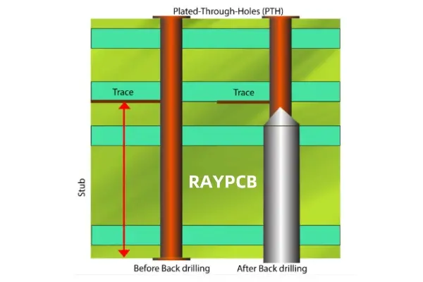
Helical Coils
- 3D spring-shaped inductor formed by plated through-hole vias
- Vias act as vertical coil segments extending over several layers
- Provides high inductance values
Toroidal Coils
- Trace loops around in a circular donut-shaped closed path
- Provides stable inductance and high Q factor
So PCB coils leverage the available copper layers to create a wound inductor structure embedded into the board itself.
How Do PCB Coils Work?
A PCB coil works on the same electromagnetic principles as wire-wound or any other inductor:
Electrical Conductor
- The copper trace acts as the conducting element, replacing the wire winding in discrete coils.
Induced Magnetic Field
- When alternating or pulsed current flows through the trace, it produces an expanding and collapsing magnetic field.
Energy Storage
- The magnetic field stores energy temporarily in each cycle of the AC current flow due to the coil’s inductance.
Developed Voltage
- Any change in applied current creates a voltage across the coil proportional to the rate of change, due to inductance.
Impedance
- The coil presents an impedance with inductive reactance which depends on the frequency.
So a PCB coil effectively behaves like a standard inductor component, with parameters determined by its construction and materials.
How are PCB Coils Constructed?
Here are some key considerations when constructing a PCB coil:
Copper Layers
- Typically use outer layers or adjacent inner layers for coiling trace.
- Can also coil across non-adjacent layers using vias.
Trace Width
- Typical widths from 0.2mm to 0.5mm based on current levels.
Trace Spacing
- Tight spacing increases inductance density but limits frequency, Q factor.
Number of Turns
- More turns increase inductance but occupy more area.
Coil Footprint
- Keep compact to minimize parasitic capacitance.
Drilled Vias
- Useful for crossing layers and anchoring ends.
Underlying Ground Plane
- Adds parasitic capacitance, but enhances Q factor and self-resonance.
By tuning these physical construction details, the PCB coil can be tailored to achieve the desired electrical parameters.
Design Considerations

Some key considerations when designing a PCB coil:
Target Inductance
- Use a calculator or modeling tool to estimate required turns, spacing, layers etc.
Frequency Range
- Optimize layout based on operating frequency band.
Q Factor
- Keep trace lengths and widths consistent for higher Q.
Self-Resonant Frequency
- Ensure it exceeds maximum operating frequency.
DC Resistance
- Wider, shorter traces reduce resistance.
AC Resistance
- Skin and proximity effects become prominent at high frequencies.
Parasitic Capacitance
- Tune layout to balance DCR with unwanted capacitance.
Available Area
- Dimension coil to fit within area and spacing constraints.
Routing Layers
- Choose layers with minimal crossing traces to reduce coupling.
- Use ground plane below coil for better Q factor.
Current Rating
- Ensure copper weight supports expected current levels.
So the PCB coil must be carefully modeled and characterized during design to achieve the target parameters.
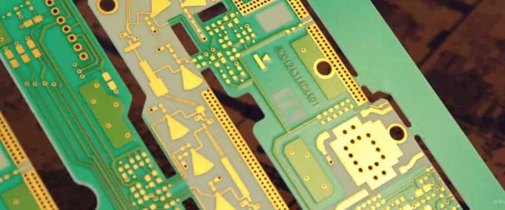
PCB Coil Fabrication
PCB coils can be fabricated using standard PCB manufacturing techniques along with other board features:
Etching
- Coil pattern is etched from copper layer using normal etching process.
Plating
- Plated through holes connectlayers and anchor coil ends.
Solder Mask
- Applied over coil surface for insulation and mechanical support.
Multilayer Alignment
- Accurate registration ensures vias connect layers properly.
Testing
- Parameters like inductance, Q factor, SRF measured to validate performance.
No special processes are required to fabricate PCB coil structures, unlike specialty components like chips inductors which need additional steps.
Applications of PCB Coils
Some common applications where integrated PCB coils provide benefits:
- Switching power supplies – for filter chokes
- Buck converters – output filter inductor
- Motor drives – supply input filters
- DC-DC converters – energy storage element
- Low noise amplifiers – gate bias coils
- Snubber circuits – energy storage and resonance damping
- Oscillators and RF amplifiers – for frequency setting and impedance matching
- EMI filters – common mode choke coils
So PCB coils are useful across a diverse range of power, motor drive and RF circuits needing integrated inductors.
Advantages of PCB Coils
Some benefits of using PCB coils rather than discrete inductor components:
Lower Cost
- Eliminates expense of inductor device and its assembly.
Space Saving
- Coil footprint matches circuit layout needs precisely.
###Simplified Assembly
- No surface mount or through-hole coil components to assemble.
Reduced Parasitics
- Integrated solution avoids wires or pads introducing parasitics.
Better Heat Dissipation
- Coil heat distributes across plane instead of being localized.
Higher Current Density
- Thicker copper traces handle more current than thin wires.
Noise Immunity
- Avoid external interference picked up by discrete coils.
Mechanical Robustness
- Coil secured structurally being part of PCB itself.
So in many cases, PCB coils present an attractive option to integrate inductors without the drawbacks of discrete devices.
Comparison with Discrete Inductors
PCB coils have some tradeoffs compared to using individual inductor components:
| Parameter | PCB Coils | Discrete Inductors |
|---|---|---|
| Cost | Lower | Higher due to device cost |
| Control over Value | Limited flexibility | Wide range available |
| Inductance Density | Higher for small values | Components can provide higher values |
| Frequency Range | Self-resonance limits high frequency usage | Some inductors support GHz range |
| Current Handling | Higher possible with thick copper | Depends on wire gauge used |
| Thermal Performance | Dissipates heat over area | Localized heating requiring care |
| Design Effort | Layout patterns can take effort | Just place part with defined specs |
So PCB coils are preferred where space, cost or assembly savings outweigh the constraints around inductance value fine-tuning.
Conclusion
A PCB coil is an inductor created from the copper traces on the layers of a printed circuit board. Various layout patterns like spirals, serpentines and helices allow constructing an embedded coil with no additional components needed. PCB coils present an attractive option for integrating inductors to save space, assembly cost and avoid performance issues associated with discrete devices. With careful modeling and characterization, PCB coils enable local energy storage and impedance directly within the board circuitry itself across a diverse range of applications.
Frequently Asked Questions
What is the typical inductance range for a PCB coil?
PCB coils can easily achieve inductance from under 1nH to about 10μH. Higher values are possible with more turns and layers, but 10μH serves many typical circuit needs as an integrated inductor.
Can you adjust the value of a PCB coil?
No, the inductance is fixed once the PCB coil is fabricated, unlike the adjustability offered by some variable discrete inductors. The coil would have to be redesigned and board re-fabricated to change its value.
Is it better to use multiple single layer coils or one multilayer coil?
For a given inductance value, usually a single multilayer coil performs better than using multiple smaller single layer coils. The mutual coupling between layers increases inductance while also enhancing the Q factor.
How thick of copper should be used to fabricate a PCB Coil?
For moderate power applications, 1 oz copper thickness is usually sufficient. For higher current handling needs, thicker 2 oz or 3 oz copper will perform better due to lower resistance.
How do you model the behavior of a PCB coil in circuit simulations?
PCB coil layouts can be imported to tools like Ansys Q3D, Ansys HFSS or COMSOL for accurate electromagnetic modeling. The simulation data can then be used in circuit simulators like SPICE to analyze the circuit behavior.