As a printed circuit board designer, you must think ahead to stay ahead of the competition. You do not want to develop a PCB that becomes obsolete shortly after production, considering the heavy investment involved. An excellent way of ensuring this not only entails producing an excellent design or contracting a top-tier manufacturer but using quality materials.
So, have you heard of Taconic EZ-IO-F? This excellent printed circuit board laminate represents the next frontier for PCB materials. It fuses top-level technology with advanced materials to ensure an unprecedented quality of PCBs for diverse applications. Want to know more? Continue reading as we delve deeper to help you understand.
In most cases, the technology and materials involved in fabricating printed circuit boards inform their names. The situation is no different with Taconic EZ-IO-F PCB. It is a type of printed circuit board that uses the thermally stable (EZ-IO-F) composite that derives its existence from nanotechnology, PTFE, and spread weave.
So what makes EZ-IO-F unique? It has nanoparticle silica, ensuring an incredible drill quality that matches the FR4 material. The laminate has a low fiberglass content with a consistent impedance and dielectric constant – all suggested through skew testing.
EZ-IO-F primarily arose for next-gen digital circuitry. However, it also got developed for microwave applications that operate at an ever-increasing frequency (high). Such higher frequencies need a combination of microwave and digital circuitry onto a single printed wiring board (PWB). By design, the EZ-IO-F challenges the finest FR4 material or laminate during fabrication
EZ-IO-F primarily arose for next-gen digital circuitry. However, it also got developed for microwave applications that operate at an ever-increasing frequency (high). Such higher frequencies need a combination of microwave and digital circuitry onto a single printed wiring board (PWB). By design, the EZ-IO-F challenges the finest FR4 material or laminate during fabrication, especially for the more complex 30 plus layer for digital applications.
Benefits of Taconic-IO-F Laminates
You can always benefit from the numerous advantages of Taconic-IO-F material. It not only confines you to enjoying very low skew and nanotech-based PTFE laminate but others as well. It encompasses an incredible drill quality akin to FR4 (a thousand hits/bits). Fr4 registration, low fiberglass content of less than 10%, and a less than 0.18% dielectric constant variation also come as benefits.
Others include:
A stable dielectric constant regarding temperature
Ability to make forty plus layers, primarily on large format printed wiring boards
Hybrid FR4-based printed wiring boards – combining digital and microwave signals.
Defense and space
What about the Skew Testing?
You mostly find skew testing proposing an utmost skew of 0.3 picoseconds per inch besides a skew average of less than 0.1ps/inch devoid of artwork rotation. A 15-degree artwork rotation demonstrates a maximum skew of 0.05 ps/inch plus a skew average of almost zero. However, the skew proves flat over a 1-20 GHz frequency.
Taconic EZ-IO-F Manufacture
EZ-IO-F mostly gets manufactured on top of no-profile copper. However, please note that the most recent ULP copper performs better than rolled copper and consequently acts as the new standard when it comes to high-performance laminates. You can achieve a lot more with rolled copper or ULP copper vs. HVLP.
If you want to achieve a strip-line channel possessing a 5 wt% fiberglass, you must combine EZ-IO-F with AGC FR-28-0040-50S with a DF of 0.0018 at 10 GHz. The AGC contains a non-reinforced prepreg that makes the strip-line properties possible. AGC prepregs (fastRise) come as the lowest commercially available prepregs, which you can then laminate at a 420-degree Fahrenheit, like FR-4.
The EZ-IO-F’s low insertion loss only compares to the PTFE laminate’s fusion bonding – a costly process that results in excessive movement. An excellent example includes operating it at 77 GHz, which compares and competes with every fusion bonding laminate favorably. What’s more, it lacks the challenges and costs common with fusion bonding.
You can obtain EZ-IO-F with a remarkably low-profile resistor foil. Further, the design of the nanoparticle, besides the absence of surface porosity, allows the etching of fine lines (a range of 2-4 mils and spaces)
You need to note that all the values illustrated are typical and not specific for distinctive purposes. Additionally, the values need to get used for single-ply construction.
If you want to design or make a Taconic EZ-IO-F printed circuit board, picking a manufacturer that can source for the specific Taconic EZ-IO-F laminate becomes important. What better place to turn to than RayMing PCB for your Taconic EZ-IO-F laminate or materials? The company will take care of your material sourcing needs and your fabrication and assembly needs. But any other top PCB manufacturer with a demonstrated PCB fabrication history can also source for Taconic EZ-IO-F laminates.
Benefits of Picking the Right PCB Material – EZ-IO-F Laminate
PCB substrates, of which Taconic EZ-IO-F laminates belong, need a careful selection to ensure the PCB designs come off. Because of this, you must consider performance during your PCB design phase for your specific application. Key performance aspects include mechanical and electrical attributes, mainly when your application areas include complicated microwave areas. Therefore, it becomes crucial to ensure mechanical and electrical reliability.
A low thermal coefficient of Dk offers electrical stability, which most engineers or designers who deal with oscillators, delay lines, and filters desire. However, the good news encompasses the fact that Taconic, Rogers, and ISOLA materials prove reliable for high-speed and high-performance applications.
Crucial Aspects to Consider in Picking a Taconic EZ-IO-F Laminate
A very low Z-axis CTE (coefficient of thermal expansion) becomes necessary if you want to get superior reliability, especially for the plated through-hole.
It is also imperative to realize a narrow positional tolerance range to match the Y and X CTE (coefficient of expansion) of the Taconic EZ-IO-F material.
Enhancing the reliability of the surface mount can be realized by limiting the solder joint stress and allowing the PCB laminate to expand. As a result, it will expand to a minimum CTE, which proves beneficial due to the low tensile modulus.
The stable dissipation factor makes it possible for you to understand how and why losses occur. It also helps in understanding their distribution across the operating frequency bandwidth.
Low (Df) dissipation factor
Thermal performance
Skew mitigation attributes
Jitter reduction
Attributes to enhance rise times
Low Z-axis CTE
Conductor loss cutback
How Taconic EZ-IO-F Compares to RF-30A and TSM-DS3M
Taconic has plenty of parts and products valuable in designing and manufacturing printed circuit boards. The EZ-IO-F, therefore, comes as one of the products. But how can it compare to other trademark products or laminates from Taconic?
Part Name
EZ-IO-F
RF-30A
TSM-DS3M
Loss factor
0.0015, 0.0014
0.0020
0.0011
Dk + Tolerance
2.80, 2.77 ± 0.05
2.97 ± 0.05
2.94 ± 0.05
Final Thoughts
If you want excellent PCB material for your printed circuit board design, you need to get a Taconic EZ-IO-F laminate. While picking a Taconic EZ-IO-F material can prove difficult, the insights provided will go a long way in picking your EZ-IO-F material.
The physical construction of printed circuit boards has changed drastically over the years, not just because of how they look. Photolithography is a process that uses ultraviolet light to etch the pattern on the surface of silicon wafers. We can only do this by using a specific combination of chemicals, making it expensive and challenging to create large-scale PCBs at scale. Keeping their size small allows electronic components like semi rigid PCBs to move through water and air without impedance or damage easily.
Electronics are becoming increasingly small and powerful. Yes, they are even miniaturizing batteries and using less power. And technology continues to change the way we live as well as work. However, there is a concern that we can no longer trust electronics without a PCB. But what is a PCB? A PCB or Printed Circuit Board stands for the electronic circuit board. It can build circuits in gadgets such as smartphones, watches, airplanes, and cars, among other things. We can see it as the brain of a device from which we can connect all its components. The PCB is best for being rigid and gives precisely what’s needed to build gadgets in a uniform and stable manner.
The good thing about this circular layout is that we can use the internal structure of the PCB to build other components like LCDs and speakers. It makes it easier for electronic device manufacturers to create products for electronic users. So, with the development and improvement of bendable circuit boards, there’s no more room for other devices. The belief is that these devices are relatively inexpensive compared to older gadgets and much simpler to use. It’s now becoming popular among people. This is because electronics manufacturing can become more budget-friendly when making PCBs. We can also use electronics in a wider range of products. Therefore, electronics companies are now also investing in this field as well.
PCBs are boards with conductive wires in a single layer, the single most crucial component of your entire device. We will connect all other components to this PCB. This makes it easier to bring all your components together because of the PCB’s good layout and design. It is also lightweight and easy to carry. With the use of a PCB, there is also less problem setting it up.
PCBs are now being helpful as flexible as well. Electronic manufacturers can now use the same materials to build bendable circuit board. It also makes it more pliable, light, and effective for solar cells, batteries, and touch screens, used more often in newer devices. This will allow users to achieve quicker performance and make electronics slimmer. Thus, it makes it harder to build with other parts of the gadgets.
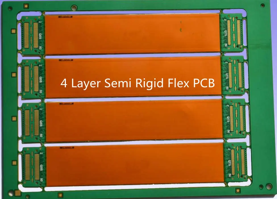
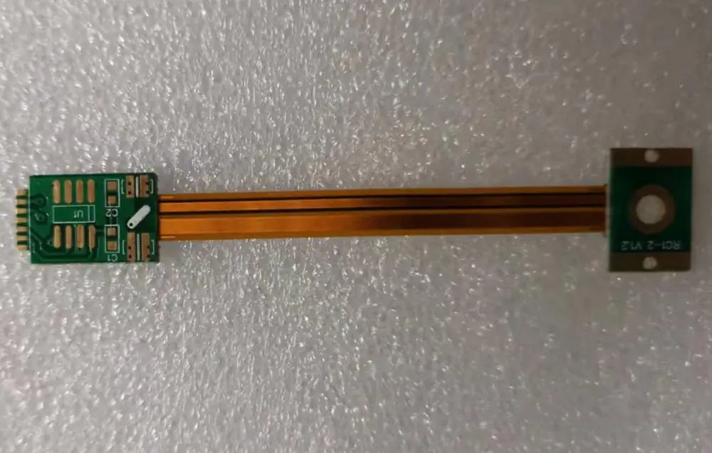
A semi rigid-Flex PCB is a flexible PCB with the flexibility and rigidity of a rigid PCB but has an external look, feel, and function of a rigid PCB. Manufacturers make the semi-rigid layer of polyethylene terephthalate (PET). It is one of the most common materials used to build flexible PCBs. PET’s main advantages are its flexibility, transparency, and toughness. They separate the semi-rigid layer with a rigid core of either FR4 or Rogers RO4003. FR4 is a glass fiber laminated circuit board material used for the PCB core. RogersRO4003 is the other commonly used PCB in producing semi rigid-Flex PCBs.
There are two types of semi rigid-flex: High Touch and Low Touch
They are flexible, transparent, and challenging. This semi rigid-flex PCB displays the LCDs and touch screens on most gadgets. It’s made of PET laminated to a rigid surface using either FR4 or Rogers RO4003. We commonly use it in devices that require flexibility and lightweight, such as tablets, smartphones, etc.
Low Touch Semi Rigid-Flex PCBs
They are flexible and tough but not transparent. We prepare it the same way as the High Touch Semi Rigid-Flex, but instead of being transparent, it is black. We use this type in devices that require less flexibility but durability, such as home appliances, smartphones, etc.
Both semi flex PCBs are durable and easily soldered together. This is especially with a low-temperature soldering iron. Solderability is one of the main factors that make these two durable and long-lasting electronics devices.
Most of the time, we use semi rigid-flex PCBs to build a device with the same function as a rigid PCB but with a different external look. Therefore, electronics need semi rigid-flex PCBs for their devices. The use of this kind of PCB will allow companies to create products and gadgets that we can use for almost any electronic device.
Advantages of semi rigid-Flex PCBs
It offers a plethora of advantages. First is the user-friendliness of the PCB. They are always lightweight, flexible, tough, and pliable, making them a lot easier to carry around and use. They also have an easy time setting them up on a board because of their lightweight, thinness, and flexibility. We can also use Flexible PCBs in building flexible devices such as solar cells, touch screens, and batteries. These are the main reasons electronics need semi rigid-flex PCBs for their products.
1. Reduced Packaging Size
When using semi rigid-flex PCBs, we will reduce the overall size of the finished product. Because of its greater versatility in its application. Since they’re flexible, they will allow electronics manufacturers to reduce their packaging sizes without compromising on the quality of the final product. When it comes to pricing, it’s cheaper compared with rigid PCBs while providing the same function. Semi rigid-flex PCBs are also easier to work with, making them more cost-effective for electronic manufacturers.
2. Weight Reduction
Semi rigid-flex PCB is best to be lighter compared with rigid PCBs. This is a great advantage for manufacturers because it allows them to reduce the weight and size of their products. With less weight and size, the product will also cost less. We can pass this on to their customers. Also, since it’s more lightweight and flexible, it will make using the finished products easier.
3. Improved Flexibility
Flexibility is one of the main benefits of using semi rigid-flex PCBs in products. Because it’s flexible, we can use it in many different applications. This means that manufacturers will have more jobs. They can use their products because it’s both flexible and tough, allowing them to develop devices with a lot more functionality.
By using semi rigid-flex PCBs, devices can have more dynamic stability. This will allow manufacturers and developers to build many more versatile products that provide high-quality performance. The PCB can also stretch, which means we can use it in many different applications.
5. Thin Profile
When it comes to performance, a thin profile is one of the essential things in devices today. We are building most of them smaller and smaller to fit inside pockets. The semi rigid-flex PCB is a lot thinner compared with rigid PCBs. This makes it easier to fit into devices, making them very light. Manufacturers need to keep their products as light and small as possible to minimize their overall weight. It will lower the cost of the finished product. We can use it in devices of extremely small size, such as smartphones, PDAs, digital cameras, etc.
6. Cost-Effectiveness
For electronics manufacturers, semi rigid-flex PCBs are cheaper than the rigid type. Manufacturers can then pass on this affordable price to end-users. This will make semi rigid-flex PCBs more popular among buyers because they provide better value for their money. Semi rigid-flex PCBs will also save them from developing extra work due to their lightweight and flexibility.
7. Environmental Friendly
Semi rigid-flex PCBs are environment friendly. Because it’s so lightweight, the products containing semi rigid-flex PCBs will be a lot lighter than other electronic devices that use rigid PCBs. This means it won’t require a lot of energy to carry, install and transport them. Also, semi rigid-flex PCBs are flexible, making them easier to recycle and repair. This is a great benefit for manufacturers because they can keep their products clean and pollution-free, helping the environment.
8. Ease of Use
Semi rigid-flex PCBs are a lot easier to use than rigid PCBs. Because they are flexible, there will be fewer cases of damages. This is because they’re pliable so that they can easily bend or twist due to accidental drops or bumps. They will also be easier to install and set up in devices since they can easily fit into tight corners because of their flexibility and thinness.
9. Impact resistance
Being flexible, semi rigid-flex PCBs are immensely impacting resistant. Even if it gets stuck, dropped, or bumped, it can still keep its original shape. This is unlike rigid PCBs, which are more prone to breaking when accidentally damaged. Since we hold the microchips and components in semi rigid-flex PCBs together by flexible solder bumps, they can be bendable PCB. The PCB will remain intact even when dropped or bumped because of this stronghold.
Nowadays, flexible PCBs are being used a lot in fabricating flexible electronics. We use them so much because they can be extremely tiny and thin, making them easy to incorporate into a wide range of applications. Today there are numerous types of semi rigid-flex PCBs that you can choose from to meet the needs and requirements of your application. However, before designing these semi rigid-flex PCBs, you must consider several factors that will affect the design process, such as:
1. Stiffeners
Stiffeners can provide a lot of strength and support to your semi rigid-flex PCBs. The stiffeners are usually copper or steel, which you will use to create your design. You can also use different materials like a crosshatch for the stiffener. It will help minimize the amount of deflection that occurs when there is an impact on your semi rigid-flex PCB.
2. Bending Requirements
Before designing your semi rigid-flex PCBs, it’s essential to consider the bending requirements that are helpful in the industry. The bending requirements can be a great help when designing your semi rigid-flex PCB. This will allow you to determine how the semi rigid-flex PCBs will bend. You can either use an inspection machine for this or use bend test equipment to check out how much deflection occurs in your design.
3. Mechanical Design
This can be an essential factor you must consider when designing your semi rigid-flex PCBs. It will help determine how your semi rigid-flex PCBs will bend. If you are using the conventional mechanical design procedure, you need to design the semi rigid-flex PCB to bend in a controlled manner. You must also consider the amount of deflection when bent and how much bending resistance occurs.
4. Solderability
The soldering process is an essential factor that you must consider when designing your semi rigid-flex PCBs. You will need to make sure that the solderability of your semi rigid-flex PCBs is not affected in any way. Also, when placing the components on the board, you must solder them to not interfere with the bending and flexing of the semi rigid-flex PCB.
5. Electronic Design
This can be an essential step you must take when designing your semi rigid-flex PCBs. You must make sure that the electronic design for the semi rigid-flex PCBs is correctly designed and not misdesigned. It will enable you to achieve your desired result. It would be best to consider how much power the semi rigid-flex PCB components require and their operating temperature range.
Below are a few tips that can help you in the design and creation of rigid-flex PCBs:
There are a lot of factors that will determine which semi rigid-flex PCBs you will choose. These include the level of flexibility, compatibility, material, and finish. The best way is to determine the application you will use to determine what you need.
1. Evade Pads & Vias at the Bend Zones
The semi rigid-flex PCBs will be more vulnerable to damage if they have excessively large and deep via holes. A good tip is to avoid these areas as much as possible in the design of semi rigid-flex PCBs. This will ensure that there are no excessive cuts or holes. It will also help improve the bond strength on their microchips and components. This prevents them from violation when bending the semi rigid-flex PCB and making it weak.
2. Make Use of Glass Passives
There are a lot of advantages that we can derive when using glass passives when designing semi rigid-flex PCBs. This is because it is an excellent insulator. It will also help protect the semi rigid-flex PCB from damage when accidentally dropped or bumped. There are a lot of advantages that we can gain from using glass passives in semi rigid-flex PCBs. These include:
It helps to keep the semi rigid-flex PCB cool even when used in devices with a high-power demand. This allows the microchips and components to remain stable. Also, it will enable them to be more flexible, reliable, and durable.
It prevents the semi rigid-flex PCB from bending too much when accidentally impacted or damaged.
3. Avoid Putting Too Many Connectors
It is best to leave a minimum number of connectors on semi rigid-flex boards with passive components. This will help reduce their weight and improve their flexibility and ease of installation. It would be best to place the connectors in areas where the board can easily access the flexing. This will avoid the need to solder them at a future date, allowing you to have more flexibility with the design.
Also, it would be best if you placed your connectors in a position where they will not interfere with the bending of the boards.
4. Use the Hatched Polygon when it comes to Copper Planes
If you are using copper pads for the semi rigid-flex PCB design, it is best to place them on a very large and broad EPP surface. This will help to improve their solderability when soldering. This will increase the bond strength and help ensure no cuts in the semi rigid-flex PCB during bending.
5. Ensure Empty Regionsare full withUnwanted Copper Traces
If you are using semi rigid-flex PCBs in mobile and consumer electronics, the need for small passives may affect the board’s overall weight. In this case, it is best to fill up all empty spaces with additional copper traces and vias. So, there will be a minimum amount of space for the semi rigid-flex PCB, which will give it a more stable structure and make it easier to bend.
6. Use Oblique Angle for Connectors
The use of oblique angles is an excellent way to reduce the resistance by half. This is because they are not perfectly perpendicular, so they will avoid selling them later. After designing your semi rigid-flex PCB, you can now design the rigid parts using Altium Designer. When designing the rigid parts, you must make sure they fit with your semi rigid-flex PCB.
Most companies manufacture all PCBs to be flexible. To state this differently, they engineer the PCBs to withstand certain levels of bending and twisting. They do not design the boards for extreme flexibility or extreme rigidity. The classification depends on the end-use of your PCB. Besides its primary use, one can engineer a flex PCB to fold or roll.
In general, flex PCBs classification includes:
1. Class 1
These are single-sided boards that are either plain or may contain special layers. They can bend just slightly, but we cannot roll them.
2. Class 2
These are double-sided boards with a rigid core surrounded by a thin layer of copper and laminate layers on both sides. Generally, we design this PCB for bending in one specific plane, like bending around the corners of a box, for example. We can roll flexible PCBs under this category but not folded because the rigid core bends when rolled.
3. class 3
We refer to multilayer flexible PCBs with special layers as “flip-chip” PCBs. These single-sided boards have one rigid layer and a flexible laminate layer on the other side. They can bend straight or roll but not fold.
4. class 4
We refer to specialized flex PCBs such as cards, backplane, and customized designs as “flexible” PCBs. They can bend in multiple directions to fit many applications like flip-chip, saddle, and half-layers
5. class 5 and 6
These are flexible laminate PCBs that are “half sheets” or “double-sided.” They contain rigid and flexible layers processed together. The degree of bending is greatly restricted and can bend in only one direction so that the maximum bending radius is about 8 mm.
6. class 7, 8, 9
These are special types of flex PCBs designed for specific applications like drones, military aircraft, and automotive electronics. Most manufacturers design them to withstand very high bending or twisting, and they do not intend to use them as flexible PCBs.
Flexible PCBs require special attention when designing rigid components. There are two reasons for this:
(1) The components like connectors can easily bend out of shape,
(2) Most connectors, pins, vias, etc., have thin walls that can easily break or bent during the design process.
There are many applications where companies use semi rigid PCBs to fit in space constraints and be very flexible. These include automotive electronics, medical devices, wearable electronics, and cell phones. Most of these use the flip-chip method to create the individually designed semi rigid board.
To manufacture a semi rigid PCB flex, the PCB component manufacturer must follow some steps like:
1. Making a small custom board
2. Making this small custom flexible PCB component
3. Mating these two together
In this way, we can have a nonflexible (rigid) part in semi rigid (flexible) PCB.
Below is a detailed diagram of semi rigid PCB process.
We make all semi rigid PCBs of three parts: solid core, laminate, and laminate on both sides. The laminated sheet only provides the lay-flat feature. They can make these components from FR4 or FR5 material by adding several layers of copper to the board. This makes the board stiffer and more resilient to bending. We make the core of the semi rigid flex PCB using a rigid material like epoxy, glass-reinforced thermoplastics, glass-filled nylon, or metal-filled nylon.
Semi Rigid flex PCBs are so versatile that we can use them in different automotive electronics, medical devices, wearable electronics, and many others. They can also be easily processed on a standard manufacturing line or a design service provider and are significantly cost-effective when the time to market.
Flexible PCBs are essential in various applications such as automotive electronics, medical electronics, wearables, and many others.
They can also be easily processed on a standard manufacturing line or a design service provider and are significantly cost-effective when the time to market.
Conclusion
Though flexible PCBs are helpful in almost every electronic device, they are still not perfect. This is because semi flex PCBs will surely be better versions of both the rigid and flexible PCBs in the future and thus more widely used. Since electronics are becoming more powerful, less expensive, and futuristic, allowing them to become more common for a wider range of products, there will be no doubt that the electronics industry will use semi rigid-flex PCBs. It seems like they are here to stay. So, with the development of semi rigid-flex PCBs, there is no doubt that electronic devices will become more powerful and better.
Do you know what a thick copper PCB is? In this guide, we will enlighten you on both the advanced and basic concepts of thick copper printed circuit boards. Reading this guide is very necessary before you go ahead to import or fabricate thick copper PCBs. This will make you an expert in the field. Before we go into details, let’s first learn what PCB is.
What is a PCB?
The full meaning of PCB is printed circuit board. This holds electric components on one platform, while offering electrical connection and structural support to the components.
Printed circuit boards decrease wire connections’ complexity, while increasing the circuit’s reliability. This allows large circuits to be created, and having this ability to link many electronic components having different functions.
Furthermore, the printed circuit board gets rid of wire complexity. It achieves this by connecting the components internally via etched conductive paths or lines.
The application of PCBs is found in various electrical equipments such as industrial machines, medical equipment, automotive industry, lighting features, and electrical appliances of different industries
Thick copper printed circuit boards contain a copper material having over three ounces for each square foot and utilized in the carrying of loads with high current.
You’ll discover that the copper material’s thickness utilized in this type of PCB falls within the range of 105 – 400 µm. Furthermore, thick copper printed circuit boards have the ability to sustain dissipation at high temperature while offering firmer connections.
In addition, this property for thermal management ensures that the thick copper PCB gets rid of thermal stress.
What is the Thickness of 5oz Copper?
In the industry of printed circuit boards, one way of expressing the thickness of copper on printed circuit boards is in ounces (oz). Now the question comes – why utilize a unit for weight in specifying thickness? Good question.
Now if copper of 1oz (approximately 28.35g) is flattened just to cover a surface area of 1 sq ft (0.093 sq meter), then the thickness that will result is 1.37 mils or 0.00348mm. Therefore, for the 5oz PCB, you should expect a thickness of 6.85 mils or 0.1740mm.
Benefits of Using 5oz PCB
Now using a thick copper PCB of 5oz, features some benefits. With this, you can use thick copper printed circuit boards in some applications.
Helps in conducting large amounts of current
With this feature, thick copper PCBs are useful in machineries or equipment having large capabilities for current like heavy machinery used in industries.
Distributes Dissipated Heat in an Impressive Manner
The 5oz PCB has great efficiency in managing thermal energy, as well as enabling the reliability of its performance. They will work fine in high temperatures and you won’t find any slack in its level of performance. In addition, this feature allows its use in any high power equipment and machinery.
Great mechanical strength
5oz PCB offers its components great foundational support, thereby making these components functionally dependable and firm. This means that it provides great support structure.
It is very compatible with some other materials
During the manufacturing of PCBs, there are other materials useful for the process of fabrication. The use of different materials could lead to compatibility problems, which leads to failure in these components. However, with 5oz PCB, there are reduced instances of these failures. This is due to the high compatibility of 5oz PCB with different materials.
5oz PCBs can serve as a very efficient option when we talk of managing the generation of heat during the process. Why this is so, is that a 5oz PCB can hold large amounts of current, and still deposit excess heat safely.
Furthermore, you will discover that your 5oz design must deliberate on your applied system’s needs. Therefore, the following are elements of design that you must emphasize.
The component’s spacing on the printed circuit board
Dimensions necessary for your PCB
Types of components you should accommodate on the printed circuit board.
Process of Fabricating 5oz PCB
You can fabricate the 5oz PCB, by the application of copper layers into the substrate.
Because copper is known to be electrically conductive, you will get a path that is conductive enough for the transfer of electric current between the components.
With respect to the application, you must consider elements of design such as type of component, spacing, and size, before you begin with the process of fabrication.
This process involves cutting the pattern into a specific surface before the highlighting of the pattern. In this case, you will pattern the conductive path’s design to the substrate. You then fill up this cut pattern with molten copper.
Plating
This has to do with adding the deposits of a material’s surface with another. You also apply this process when fabricating 5oz pcbs. Here, you deposit the copper to the substrate working with the design of its conductive path.
Concerning these processes above, you perform them on the substrate. This is achieved by making use of sidewalls, as well as holes using printing screens.
It is possible to design a 5oz PCB. This is possible using computer-aided softwares. You will find these softwares easy to use in both industrial labs and academic halls. This allows you to develop your desired PCB designs elaborately.
The softwares can either be web-based or OS-based. This software is useful in designing the diagrams of the circuit, as well as editing them schematically. Furthermore, some software offers simulation, which allows users to both export and import the desirable features into the layout of your PCB.
In addition, some permit the visualization of 3D design, coupled with allowing the incorporation of all the components of your circuit into your design. You can achieve all these from anywhere, as these softwares support different languages.
Conclusion
You can produce 5oz pcb either through plating or etching. This pcb also comes with different benefits, which makes them come with high demand. As a result of its great benefits and features, 5oz pcb will surely meet your electrical demands and requirements.
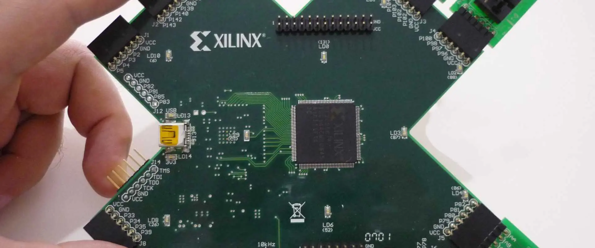
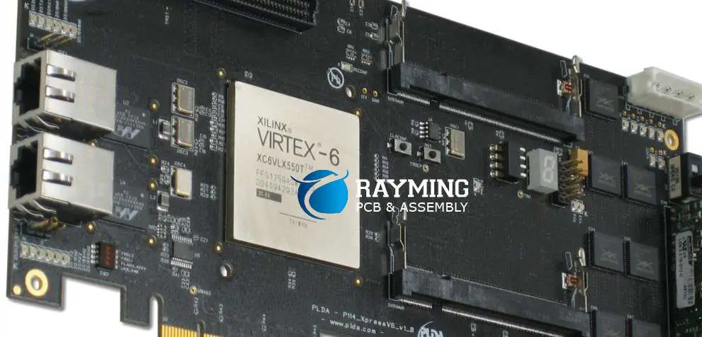
The Xilinx boards are a magnificent piece of hardware from Xilinx designed for the latest FPGA technology. They are a multipurpose board that meets the ever-changing needs of FPGA users. It comprises two different models, the extended Spartan 3A and extended Spartan 3AN.
The electronics industry is moving fast towards the chip-to-chip connection using FPGA technology. The Xilinx boards provide access to both the onboard and expansion ports for easy integration with other chips. The boards have a serial flash memory for the nonvolatile storage of data. Additionally, it also has a flash memory operating in SPI mode that is accessible from the onboard USB port. The boards support the standard and extended Xilinx configuration programs and data files for different FPGA chips.
The boards support a wide range of FPGA architectures. For instance, 20,000 physical logic cells (10Mbit) – 4k x 16 general-purpose logic (gpl) cells – 10k x 32 gpl cells (2x16k bit).
The Xilinx boards are perfect for the lowest power, maximum performance FPGA. They provide a fast and flexible interface for all types of applications. The Spartan 3A is ideal for designing custom FPGA chips in small and medium-sized. We can configure them either standard or extended during the hardware setup. As a result, most people use it in instrumentation and control applications. For instance, digital oscilloscopes, multifunction I/O test equipment, or high-performance computing platforms.
The Spartan 3A is for users who want the simplest and most cost-effective FPGA from Xilinx. It has 12 digital input/output pins. The Spartan 3A is ideal for programming the FPGA chips in an embedded design.
The Spartan 3A has two onboard antennas that we can use in wireless communication systems like Bluetooth, ZigBee, and Wi-Fi (802.11).
Extended Spartan 3AN
The Xilinx boards extend the capabilities of the Spartan 3A to include one more memory configuration. An extended memory configuration.
The extended memory comprises four zones with configured-on-board flash, SPI, and Serial Peripheral Interface (SPI) memories. The Spartan 3A’s onboard flash memory has a capacity of 4k x 16 bits with a fast cycle time of 2ns. So, the SPI flash has a capacity of 32k x 16 bits with a fast cycle time of 2ns. The onboard flash is essential in storing configuration data for standard memory configurations. The onboard flash is also accessible from the host computer USB port for programming purposes.
The extended memory is also accessible from the host computer USB port for programming purposes. The SPI flash is essential in storing configuration data for the extended memory configurations. We also use the SPI flash as nonvolatile storage and can reprogram it using Xilinx’s software for configuration and data updates. The SPI integrated into the Spartan 3A can communicate with off-chip memory or other devices over various applications. For instance, personal digital assistants (PDAs) and mobile devices, phone handsets, etc.
History of the Xilinx Extended Spartan-3A/AN FPGA Boards
xilinx-spartan-6-fpga-tutorial
The Xilinx is an American-based multinational company that is one of the largest suppliers of FPGA and software for technology globally, with more than $1billion. It has been in operation for over 40 years, and its market capitalization exceeds $9 billion.
Ross Freeman founded the company in October 1983, along with Bernard Vonderschmitt, formed Xilinx Inc. The corporation’s headquarters are in San Jose, California. The company was formerly known as MOS Technology Inc. up until their name changed to Xilinx in 1998. The Xilinx boards are available at a nominal cost from several distributors, including Digi-Key.
It is almost certain that the boards are available to the public domain through resellers. Still, there are no technical specifications or files found anywhere on the Internet for these devices. People widely use boards in many industries. For example, aerospace and defense, automotive and transportation, energy, and natural resources. The company is constantly competing with Altera Corporation in the FPGA industry.
We can use the Xilinx boards to program an FPGA chip in a variety of configurations. The boards provide the easy programming of the FPGAs via a USB cable. Additionally, the board has serial flash memory for the nonvolatile storage of data. Top users of these boards include RayMing PCB and Assembly.
Features
Xilinx FPGA boards are available in a wide range of configurations. The latest addition to the Xilinx family is the Spartan-6, which offers 12 digital input/output pins. As a result, the board has two onboard antennas that we can use for wireless communication applications like Bluetooth, ZigBee, or Wi-Fi (802.11). Common features include:
On-Board Flash Memory:
The onboard flash memory helps in storing the configuration settings for the FPGA board. This storage function helps set up the FPGA board at different locations. It helps maintain the continuity of much data when plugging another unit into a system. The Spartan-3A’s onboard flash memory has a capacity of 4k x 16 bits with a fast cycle time of 2ns. The SPI flash has a capacity of 32k x 16 bits with a fast cycle time of 2ns.
On-Board Antennas:
We can use the two onboard antennas with the FPGA boards for wireless communication applications like Bluetooth, Wi-Fi, or ZigBee.
Xilinx is one of the major players in the FPGA industry. It makes it possible to have all their products available at a nominal cost from numerous distributors, including Digi-Key.
Clock Sources:
The Spartan-3AN board has a clock source that we can use with the FPGA for synchronizing with another hardware or software program. The FPGA has a clock input and output, which is very important in the operation of many applications. The Spartan-3AN board has a Real-Time Clock (RTC) to help maintain the system’s time and date. This helps in synchronizing the FPGA with another hardware or software program.
The programmable logic blocks can install complex functions using the hardware description language. The programmable array logic and the programmable logic devices perform complex logical operations. These two types of circuits are also known as field-programmable gate arrays. They help customize the circuit function.
Character LCD Screen:
The LCD screen is a very useful tool for a technician to use. We can use it to verify the programmed design and provide a visual representation of the FPGA data. The LCD screen has a specific band that we can be program using the software. The user can display various configuration settings, clock values, fault values, and other information.
Network Interface:
The Spartan-3AN board has an onboard network interface to help connect with other network devices such as personal computers or servers. We can connect the board to a network using a 10/100 Mbit Ethernet LAN interface, commonly used for networking.
USB Interface:
The Xilinx board has an onboard USB interface that makes it easy to connect with other peripheral devices using USB cables. We can use these cables for synchronizing data between two devices. This feature is convenient for transferring data between the flash memory and the computer’s hard drive or vice versa.
Power Source:
The Spartan-3AN board uses a 7 V to 16 V power supply system. It makes it adhere to all electronic test equipment (ETE) and can power up/down and loading/unloading memories.
VGA Display Port:
The Xilinx board has a VGA display port connected to the host computer using the video adapter. The video port is an interface that connects to the VGA display. It does it through technical standards for digital data transfer, such as DVI, HDMI, DVI-D, and others.
Dual UART:
The Xilinx board also has a dual UART with two channels, which can communicate with the host computer using serial port communication. The UART is an interface that we can use for asynchronous data transfer from one device to another. For instance, from the computer to the Xilinx board or vice versa.
Xilinx Extended Spartan-3A/AN FPGA Boards design
The Xilinx extended Spartan-3A/AN FPGA boards design makes it easy to create a custom design. The user can use the embedded Logic Analyzer, and the onboard debug probe to find out why their design is not working as desired.
The Xilinx FPGA board comes with a Spartan-3AN FPGA, which one can reprogram using a computer and Vivado Design Suite software. The user needs to use the programming software to connect with the Spartan-3AN board through a USB cable.
The Spartan-3AN FPGA has more than 1,000 digital and analog inputs and outputs. There is also a VGA display port and an onboard network interface, connecting with other servers or personal computers. We can use the onboard flash memory of the Xilinx board for storing data of more than 1MB. The Spartan-3AN board also has a PAL and a PLD to implement complex functions in the digital world.
Some of the advantages of using the Xilinx Extended Spartan-3A/AN FPGA Boards include:
1. Performance
The Xilinx Extended Spartan-3A/AN FPGAs provide high performance, which we can enhance using a clock source. The FPGA has a clock input and output, which is very important in the operation of many applications. These boards have a fast cycle time of 2ns. Compared with the Spartan-3A, this board has eight digital inputs/outputs and six programmable logic blocks. The user can implement complex functionality using hardware description languages (HDL).
2. Customizable designs
We can customize the Xilinx extended Spartan-3A/AN FPGA boards using the hardware description language to fit the user’s design criteria. The user can create complex designs using this board, which we can then implement into their system. All the standard elements present in a Spartan-3A/AN FPGA are also present in this board. These include flip-flops, D-type latches, and a DSP48E1 processor. The flip-flops can create stable circuits, while we use the D-type latches to store multiple data bits. The user can also create more complex designs with the help of loopback paths, which are present in these boards.
3. Cheap
The Xilinx extended Spartan-3A/AN FPGA Boards are very cost-effective. It makes them easy to obtain and implement in commercial applications. The user can get several boards cut for a fraction of their cost without compromising on the performance. The extended Spartan-3A/AN boards are also reprogrammable, making it possible to use the same boards multiple times.
4. Support for older Spartan FPGAs
The Xilinx extended Spartan-3A/AN FPGA Boards support an older Spartan family of FPGAs as well. This makes them cost-effective for users who may not wish to change their boards manually, even if their FPGAs require upgrades. The Xilinx extended Spartan-3A/AN FPGA boards can upgrade older Spartan FPGAs and make them compatible with newer features.
We can expand the Xilinx extended Spartan-3A/AN FPGA Boards with more digital inputs and outputs. It expands the functionality of the current board. One makes this possible using IC sockets on these boards. The user can create an entire system of their own with the help of these boards.
6. Multiple options for programming
We can program the extended Spartan-3A/AN FPGA boards using several preferred options: USB, Ethernet, and clock lines. The onboard flash memory makes it possible to store data that we can retrieve at any time using any of these options. This offers the user great flexibility when deploying their designs into real systems.
7. Availability of FPGA design software
The Xilinx extended Spartan-3A/AN FPGA boards come with several pieces of software that we can use for programming the user’s designs. These include Xilinx ISE, the industry standard for HDL programmers, and development systems for different programming languages such as VHDL and Verilog.
8. Low power consumption
The Xilinx extended Spartan-3A/AN FPGA Boards provide low power consumption compared to the usual FPGAs. We can attribute the low power consumption of these boards to their architecture. It does not perform as many operations as other boards. This makes them ideal for places where there is a problem with excess heat and noise, such as factories and data center environments.
9. Education
The Xilinx extended Spartan-3A/AN FPGA Boards are excellent for educational institutions. Especially for students learning about FPGAs. We can use these boards to create exciting designs that the user may deploy in the future. The user can also learn more about HDLs. It will increase their knowledge of hardware-oriented programming languages.
Limitation of Xilinx Extended Spartan-3A/AN FPGA Boards
The Xilinx extended Spartan-3A/AN FPGA Boards have several limitations as well:
1. Compliant with ISO 26262
The Xilinx extended Spartan-3A/AN FPGA Boards only comply with the ISO 26262 specification. This means that we cannot use them in disaster and industrial systems. The user will also need to ensure that they mount the board safely, verified beforehand before deployment.
2. Low-quality I/O pads
The Xilinx extended Spartan-3A/AN FPGA Boards use low-quality pad patterns. It is incompatible with specific operating environments. The pads can short circuit, which can cause severe damage to the board and the system.
3. High power consumption
The Xilinx extended Spartan-3A/AN FPGA Boards have a high-power consumption of 300 mW. It makes them unsuitable for use in areas with strict environmental conditions. The high-power consumption can cause the board to overheat, which is a risk in industrial areas.
The Xilinx extended Spartan-3A/AN FPGA Boards have a low-quality PCB. It can cause problems with the board’s stability and reliability. The user should not use these boards for critical applications in applications that require high reliability and stability. This is especially true when we use it in industrial environments where there are strict environmental conditions.
5. USB output power
The Xilinx extended Spartan-3A/AN FPGA Boards have a limited amount of power on the USB port, which can cause problems with the user’s application. The user should use a separate research power supply for their designs, as drawing enough current from USB ports may not be possible.
6. Cannot reprogram
You cannot reprogram the Xilinx extended Spartan-3A/AN FPGA Boards with specific programming languages. It limits users’ ability to modify their designs. The user should look for a board that supports whichever programming language they prefer.
7. Incompatible with LVDS
The extended Spartan-3A/AN FPGA boards are incompatible with LVDS. It makes them challenging to use in some industrial applications. The user should look for boards that support LVDS to avoid such problems.
8. Low throughput
The extended Spartan-3A/AN FPGA boards have low throughput. It makes them less suitable for industrial applications. The user should look for boards that support higher Throughputs. It ensures compatibility with the application’s hardware interfaces.
9. Low efficiency
The extended Spartan-3A/AN FPGA boards are inefficient compared to other FPGAs. It is an issue for industrial applications where power is expensive. The user should look for boards that run on a lower power supply to avoid spending excess money on power at the end of their designs.
10. Incompatible with other FPGAs
The Xilinx extended Spartan-3A/AN FPGA Boards are not compatible with other FPGAs from Xilinx. It is an issue when the user needs to use different types of boards for their designs.
We use FPGA boards in various systems. Some of the applications include
1. Printed Circuit Boards (PCBs)
The Xilinx extended Spartan-3A/AN FPGA boards can design Printed Circuit Boards (PCBs) for digital systems. These boards can develop PCBs for consumer products, such as memory cards, cell phones, and video game consoles. The boards are also suitable for use in military applications since they are compliant with several safety certifications. They are also ideal for use in industrial environments, especially in systems that require low noise and high reliability.
2. Smart grid
We can use the extended Spartan-3A FPGA boards to develop smart grids for managing energy consumption. These boards are ideal for use in these systems because they have a high speed of processing data. It allows them to collect real-time information on the consumption and distribution of energy. This makes them more efficient than traditional systems. It cannot process this information simultaneously due to limited computing power.
3. Security
We can use the extended Spartan-3A/AN FPGA boards to design security systems. Additionally, we can use these boards for energy management, smart cards, and biometrics applications. The user can use this board to create encryption algorithms resistant to attacks. It establishes secure systems that prevent unauthorized access. This makes them ideal for military, intelligence agencies, and government networks. It requires high security in its operations.
4. Industrial Control System (ICS)
The extended Spartan-3A/AN FPGA boards can manage industrial and process control systems. We can use these boards to manage and control internal processes, such as material transport and storage. This makes them ideal for use in the food and beverage, medicine, and oil industries. It requires secure and reliable processes to ensure optimum production output.
5. Wireless networks
We can use the Xilinx extended Spartan-3A/AN FPGA boards to create wireless networks. Additionally, we can use these boards to develop mobile devices, such as smartphones and tablet computers. The user can use this board to create 802.11 wireless networking systems. It is ideal for use in areas requiring high-speed data transmissions, such as vehicle dashboards and Wi-Fi access points.
6. Automotive
The Xilinx extended Spartan-3A/AN FPGA boards can create automotive systems. We can use these boards to design infotainment units for vehicle dashboards and systems that control the vehicle’s fuel supply and airbags. The user can also use this board to create a diagnostic tool to read a car’s ECU data. It helps prevent breakdowns and other problems that arise during a car’s operation.
7. Real-time systems
The extended Spartan-3A/AN FPGA boards can create real-time systems. We can use these boards to develop embedded processors. For example, smart digital watches and calculators, and guided-missile tracking devices, and other applications that require real-time processing.
Tools and software packages written specifically to use with these boards:
1. Nios II
We can program the Xilinx extended Spartan-3A/AN FPGA Boards using Nios II, a soft processor for embedded systems. We can use Nios II to develop compact and reliable motor control systems and power distribution units with high system integration.
2. LabVIEW
LabVIEW is a graphical programming language developed by National Instruments Corporation. This software allows the user to create programs that control various hardware devices. It includes signal processing devices and robotics controllers. The user can use LabVIEW to create systems for controlling processes in industries such as oil and gas and systems for testing engines and other components.
3. MATLAB
MATLAB is a high-level programming language developed by MathWorks. This software allows the user to develop control, simulation, and data analysis programs that are easy to modify. Moreover, we can use MATLAB for various purposes, including creating control room displays, real-time processing systems for wireless networks, and automation of production processes in industries such as oil refining.
4. AVR Studio/GCC
We can program the extended Spartan-3A FPGA Boards using AVR Studio, which Atmel Corporation developed specifically to program embedded devices. Since this is an open-source compiler, the user can use the tool for compiling C programs for different programming types of components and systems running on different operating systems. So, the user can use this tool to create low-power microcontrollers for motor control systems and PWM generators for wireless technology.
5. MCS Software
We can program the Xilinx extended Spartan-3A/AN FPGA Boards using MCS Software. Xilinx developed it in collaboration with Mentor Graphics Corporation. This software allows the user to develop software for creating processors that run on specific hardware devices. The user can use this software to create low-power controller systems embedded in water meters, turnstiles, and high-performance microcontrollers that run high-end robotics systems.
Xilinx Extended Spartan-3A/AN FPGA Boards
Common specifications include:
Made In Japan
Non-use of 6 Restricted substances of RoHS directive
· XC3S1400A: 8 DCMs, 32 Multipliers, 576 K Total Block RAM Bits, 100 Maximum user I/O pins (Board), 161 Maximum user I/O pins (Device), 176 K Maximum Distributed RAM Bits, 25,344 Logic Cells, and 1400 K System Gates
· XC3S700A: 8 DCMs, 20 Multipliers, 360 K Total Block RAM Bits, 100 Maximum user I/O pins (Board), 161 Maximum user I/O pins (Device), 92 K Maximum Distributed RAM Bits, 13,248 Logic Cells, and 700 K System Gates
· XC3S400A: 4 DCMs, 20 Multipliers, 360 K Total Block RAM Bits, 100 Maximum user I/O pins (Board), 195 Maximum user I/O pins (Device), 56 K Maximum Distributed RAM Bits, 8,064 Logic Cells, and 400 K System Gates
[XCM-304] Xilinx Spartan-3A VQG100 FPGA board
· XC3S200A: 4 DCMs, 16 Multipliers, 288 K Total Block RAM Bits, 48 Maximum user I/O pins (Board), 68 Maximum user I/O pins (Device), 28 K Maximum Distributed RAM Bits, 4,032 Logic Cells, and 200 K System Gates
Conclusion
The Xilinx extended Spartan-3A/AN FPGA Boards provide the user with a power-efficient and cost-effective option for implementing their designs in real systems. These boards are straightforward to use, making them ideal for learners and professionals alike. The user can deploy their designs once and then implement them several times using the same boards using different programming languages. The Xilinx extended Spartan-3A/AN FPGA Boards also provide low power consumption due to their architecture.
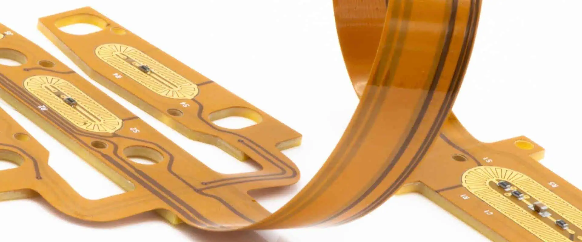
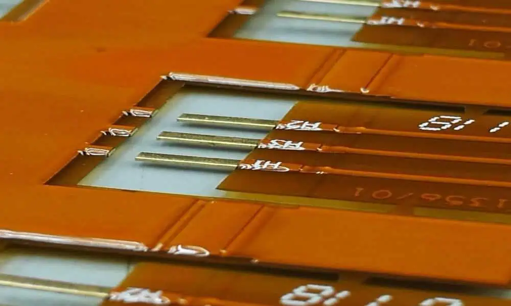
Flex Printed Circuit Boards (PCBs) provide unmatched design flexibility, enabling innovative solutions across industries like aerospace, medical devices, and consumer electronics. Renowned for their ability to bend and fold, flex PCBs deliver substantial space and weight savings, making them ideal for compact and lightweight applications.
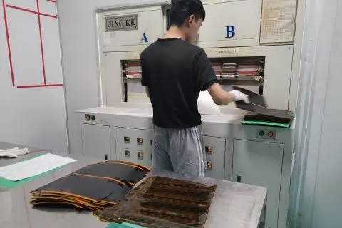
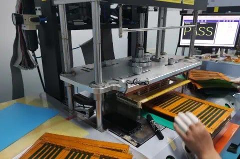
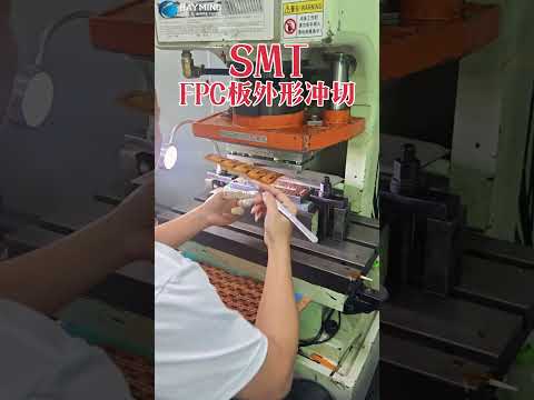
Below, explore our image gallery showcasing the flex PCB manufacturing process. From material preparation and etching to drilling, plating, and final fabrication, each step is meticulously executed to ensure precision and quality.
What is Flex PCB?
Let’s start with the basics. A Flex PCB, or Flexible Printed Circuit Board, is exactly what it sounds like – a circuit board that can bend! Unlike their rigid cousins, Flex PCBs are made with materials that allow them to twist and turn without breaking.
Why are Flex PCBs so cool? Here’s why:
They’re bendy: You can fold them without damaging the circuits.
They’re light: Much lighter than regular PCBs.
They’re space-savers: Perfect for tight spots in gadgets.
They’re tough: They can handle shakes and vibrations better.
They’re good with heat: They can spread heat more effectively.
These features make Flex PCBs perfect for smartphones, smartwatches, and even cars!
First things first, we start with cleaning. The flexible material (usually polyimide or polyester) is thoroughly cleaned. It’s like giving the PCB a bath before its big day!
2. NC Drilling
Next up, we drill holes. But not just any holes – precise, computer-controlled holes. These will help connect different parts of the circuit later.
3. Copper Plating Process
Now, we give the board a copper coat. This step is crucial because copper is what makes the board conduct electricity.
4. Dry Film Lamination
Think of this step as putting a sticker on the board. We apply a special light-sensitive film that will help us create the circuit pattern.
5. LDI Exposure
Here’s where it gets cool. We use lasers to draw the circuit pattern on the film. It’s like a high-tech laser show, but for circuit boards!
6. Develop /Etch/ Stripping
This step is a bit like developing a photograph. We remove parts of the film and copper to reveal our circuit pattern.
7. AOI Testing
Time for a quality check! Cameras inspect the board to make sure everything looks good. It’s like giving the board an eye test.
8. Coverlay Layup
Now we add a protective layer called the coverlay. It’s like putting a jacket on the circuit to keep it safe.
9. Coverlay Lamination
We use heat and pressure to stick the coverlay to the board. It’s like ironing the jacket onto the circuit.
10. Hole Punching
We punch more holes for things like mounting the board or connecting components. Precision is key here!
11. Surface Finish (Immersion Gold)
We give the board a golden touch. This thin layer of gold protects the copper and makes it easier to solder components later.
12. Silkscreen Printing
Now we add labels and markings. It’s like giving the board its own set of instructions.
13. Electrical Test
Time to see if it works! We run electricity through the board to check if all connections are good.
14. Stiffener Application
Some parts of the board need to be rigid. We add stiffeners to these areas, like giving the board a backbone.
15. Outline Punching
We cut the board to its final shape. It’s like giving the PCB its unique identity!
16. FQC (Final Quality Control)
One last check to make sure everything is perfect. We inspect the board from top to bottom.
17. Package and Shipping
Finally, we wrap it up and send it off. The Flex PCB is ready for its new home in a cool gadget!
Single Layer vs. Double Layer: A Tale of Two Flex PCBs
Flex PCBs come in two main flavors: single-layer and double-layer. Let’s see how they differ.
Single-sided Flexible PCB: The Simple Sibling
Single-sided Flex PCBs have circuits on just one side. Here’s a quick rundown of how they’re made:
Cut the material
Drill holes
Add the circuit pattern
Protect the circuit
Add finishes and labels
Test and ship
It’s simpler and cheaper, perfect for basic designs.
Double-sided Flexible PCB: The Complex Cousin
Double-sided Flex PCBs have circuits on both sides. Their manufacturing process is a bit more involved:
Cut and drill
Add circuits to both sides
Connect the two sides
Protect the circuits
Add finishes and labels
Test thoroughly
Cut to shape and ship
This type allows for more complex designs but takes more time and money to make.
Wrapping It Up
And there you have it! From a simple flexible sheet to a high-tech, bendable circuit board, the journey of a Flex PCB is quite amazing. Whether it’s the simpler single-sided or the more complex double-sided version, these flexible marvels are changing the way we design electronics.
Next time you use your smartphone or put on a smartwatch, remember the incredible process behind the flexible circuits that make it all possible. The world of Flex PCBs is constantly evolving, paving the way for even cooler, more flexible gadgets in the future. Exciting times ahead in the world of electronics!
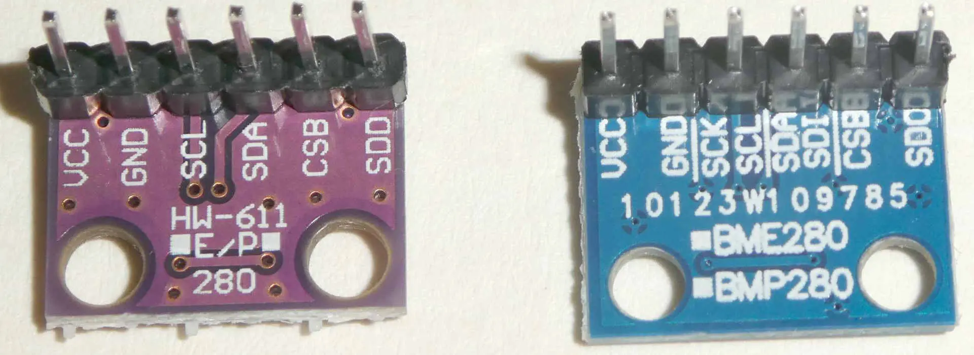
While searching for some affordable environmental sensors, we came across the popular and seemingly ideal BME280. This sensor is the digital I2C type, which can function at either 1.8V or 3.3V, offering measurements of barometric pressure, humidity, and temperature consuming low energy in the process and working with high accuracy at affordable and low cost. This is why it is great for temperature monitoring, weather stations, etc.
Due to this, we decided to buy some BME280 sensors from some sellers. However, on two occasions, we got BMP280, which is lesser compared to the BME280. The difference between bmp280 vs bme280 is that the BMP280 has a different ID and lacks humidity measurement. So using the BMP280 didn’t give the desired results and it felt like we made a mistake. This is why we are writing out this information to help you in case you have been supplied a different product and don’t know the difference between bmp280 vs bme280.
The grove barometer sensor has a high precision and low-cost sensor, which measures the barometer and temperature. Furthermore, this sensor supports the SPI and I2C communication.
It is known as a tiny and cheap atmospheric sensor breakout that helps in measuring barometric pressure and temperature, without having to take up much space. You can get everything you need to know just from its tiny breakout.
This breakout was specially designed for outdoor/indoor navigation, home automation, weather forecasting, wellness monitoring, and personal health. The module makes use of Bosch-manufactured environmental sensors with barometric pressure, temperature sensor, which is the upcoming generation upgrade of the well known sensor BMP183/BMP180/BMP085.
This sensor serves all weather sensing types and will even work effectively for both SPI and I2C. This Bosch’s precision sensor is regarded as the best precision sensing, low-cost solution for the measurement of barometric pressure having an absolute accuracy of ±1.0 hPa and a temperature measurement accuracy of ±1 degrees centigrade.
Due to the fact that pressure changes with respect to the altitude, the measurements of pressure are so accurate and good that it can also serve as an altimeter having an accuracy of ±1.0 meter.
BMP280 can be regarded as the next generation of sensors. It upgrades the BMP183/BMP180/BMP085 having altitude with low noise of 0.25m. Its conversion time is also similar and fast. Specifications here are also the same and can utilize either SPI or 12C. For easy and simple wiring, choose 12C. Also, if you wish to connect some sensors without having to worry about the collisions of the 12C address, then choose SPI. Just like the BME280 sensor, the BMP 280 can also serve as an accurate altimeter too.
Specifications of the Grove BMP280 Barometer Sensor
Dimensions 20mm x 40mm
Current Consumption 0.6 mA
Supply Voltage 5V or 3.3V
Barometric Pressure Accuracy ±1.0 hPa
Barometric Pressure Range 300 – 1100 hPa
Temperature Measurement Accuracy ±1
Weight 3g
Temperature Measurement Range -40 to 85
BMP280 Applications
You may be asking where the BMP280 sensor is useful. As a result of its features and capabilities such as its SPI and I2C compatibility, the BMP 280 sensor is great for any type of weather, as well as environmental sensing. Below are some of the applications of the BMP280.
Outdoor navigation (sports and leisure applications)
Indicating vertical velocity
GPS navigation enhancement (dead-reckoning, detection of slopes etc)
Applications relating to health care i.e. spirometry
All other projects requiring appropriate reading of the atmospheric pressure
Why is my BMP280 Not Starting?
Have you encountered a scenario where your BMP280 is not starting? If you possess a breakout board that lacks level shifters, then you go ahead to create some making use of some components, just to get the I2C mode moving on, and next, you burn the code into the uno r3 of the Arduino. You will then be surprised to see nothing happening.
For real engineers, you’ve made an attempt, but now it is high time you went through the manual. Usually this is the last resort. After going through, you will discover that the BMP280’s communication mode is fixed on power up made possible by the state of the different control inputs.
SPI utilizes more pins because it helps in defining its interface. Imagine one is unused as the outputs in the SPI mode, and the other used as input in the I2C mode! Take for instance you possess a breakout board, then the control inputs will be left floating. This means it will not just function until you make sure they are properly set before you power up.
BME 280 can be referred to as an environmental sensor integrated by Bosch, which measures temperature, pressure, and humidity. By this, users will get a holistic and comprehensive measurement of their environment.
Furthermore, the sensor shows a quick response time to aid in supporting performance requirements, coupled with high accuracy. Asides from this, it is optimized for high resolution and low noise.
For bme280, we will be considering the environmental sensor, how BME280 is relevant to our world today, as well as other sensors related to the BME280.
This sensor is based on the Bosch BME28. This BME28 is known for its high-precision, low-cost, and its ability to support both SPI and I2C communication.
The Grove BME280 offers an accurate measurement of the environment’s humidity, temperature, and barometric pressure.
Due to its great accuracy during pressure measurement, and changes of pressure with altitude, it becomes easy to calculate its altitude with a meter accuracy of +1. This also makes it an accurate and precise altimeter.
Furthermore, there’s no need to be concerned about I2C collisions, because it offers both SPI and I2C interfaces. In order to make use of the SPI, just desolder its bonding pads, which are found on the back of the breakout board of the BME280. For I2C, its board also offers two I2C addresses, giving you the option of choosing whichever you want.
Also present are libraries that have high abstracts. This ensures that users can use the BME 280 to build their projects faster and quicker.
Specifications of theGrove – BME280 Environmental Sensor
You may have asked what groove is all about. Grove can be described as the personal modular of Seeed. It is also its standard connector prototyping system.
For Grove to help in assembling electronics, Grove utilizes an approach called building block. In contrast to the solder or jumper based system, connecting, building, and experimenting it is easier. This ensures that the system of learning is easy for the hobbyists. You don’t have to worry because it doesn’t get to a point when it begins to dump down.
You may be asking where the BME280 sensor can be applied. As a result of its features and capabilities such as its SPI and I2C compatibility, the BME 280 sensor is great for any type of weather, as well as environmental sensing. Below are some of the applications of the BME280.
Monitoring of fitness
Control of home automation
Forecast of weather
Indoor or outdoor navigation
GPS navigation enhancement
All other projects requiring appropriate reading of the atmospheric pressure
BME280 use with Arduino
You can use the environmental sensor Grove-BME280 with different microcontrollers such as Arduino, LinkIt ONE, and Beaglebone. You can achieve this through SPI or I2C. For our example today, we will be explaining to you how to connect your Grove environmental sensor BM280 to the Arduino.
Step by Step Guide
Step One: Connect the BME280 sensor to touch the Grove Base Shield V2 I2C port. After that, plug or insert it to Seeeduino. However, if you lack a Grove Base Shield, the module can be connected directly to the Seeeduino
Step Two: Using a USB cable, connect Seeeduino to the PC
Step Three: Here is the software aspect of the tutorial. First of all, visit Github to download the example and library code.
Step Four: Create a brand new sketch for the Arduino and then paste some codes to it. You can also get access to the code directly just by following this path: File – Example – Barometer_Sensor – Barometer_Sensor
Step Five: This step requires that you upload this code gotten in step five into your Arduino
Step Six: Open the serial monitor in order to receive the data of the sensor, which includes humidity, altitude, value of barometric pressure, and temperature.
That’s all. In these six steps, running the BME280 sensor with Seeeduino becomes very easy. Now let’s consider another sensor related to the BME280, which is the bmp 280.
The BMP280 shares similarities with the BME280. Also, they also have a very similar parameter performance. This is why people usually get confused.
However, we will clarify both. BMP 280 can measure just the air pressure and temperature. However, the BME280 can only measure humidity coupled with air pressure and temperature.
Due to this difference, you will get the BMP280 at a much cheaper rate compared to the BME280.
Furthermore, the barometer sensor BMP280 can be seen as a much better development to the barometer sensor BMP180. Also, the environmental sensor BME280 adds the measurement of humidity to the BMP280.
Therefore, if you wish to get just the atmospheric pressure, we advise that you utilize the BMP280. However, if you wish to monitor your environment comprehensively, then we advise that you choose the BME280.
Other ways of detecting differences between bmp280 vs bme280 is by inspecting the pcb visually and by inspecting the package.
Inspecting the PCB visually
Also, you can see the difference between bmp280 vs bme280, just by inspecting the PCB visually. Checking the rear of the PCB, the one colored uniquely with the right printing is genuine. If the P text is covered with a black dot on its module and sold as a BME280, then it’s wrong. This is because the P text, which is hidden or covered, clearly indicates that it is BMP280. Original modules usually don’t come with a mark.
Inspecting the package
Finally, you can know the difference between bmp280 vs bme280 just by inspecting the package visually. If you check the datasheet of the BME280, you will see the markings for devices requiring mass production. This marking has to have ??? U? format. Here, the U signifies BME280. Now, the last ? you are seeing here is just a P, while the final two characters are supposed to be UP.
Comparing with the datasheet of BMP280, the format ought to be ??? K?. Here, the final “?” should be either W, N, U, P. Therefore, KW, KN, KU, KP are all devices of BMP280.
After reading through, you will come to understand that there are some differences between BMP280 vs BME280. If you decide to buy BME280 online, there’s a great chance that what you’ll get is the lesser BMP280. This is because some of these sellers simply don’t know what they are selling. Also, they simply don’t understand the difference between bmp280 vs bme280. Also, the break-out design of a PCB, which is shared between two different sensor types. Due to this reason, it could be frustrating when you buy these sensors. This is because sellers usually do this without getting caught.
To be sure of whatever you have ordered, you will have to spend some more money for modules from industries like Adafruit. Here, everything is properly controlled and labeled.
For most of us, telling the difference between a flex board and a rigid-flex board design needs to be effortless. Well, it all is until it is not. So let us try this: enumerate all the differences you can think of – can you? I thought not.
However, understanding the distinction between flex and the rigid-flex board can make or break your PCB design. You must navigate all the intricacies and master the ruses involved if you want a functional and efficient PCB for your application. But first things first, what is a flex board design? What is a rigid-flex PCB design?
This article seeks to exhaustively tackle the difference between flex board design and rigid-flex design.
What is a Flex Board Design?
A flexible PCB design, often called a flex board design, comes well patterned (printed circuitry) with components that use flexible-based materials. It can either have or lack a cover-lay material.
Like you, most electronic engineers have gotten accustomed to rigid PCB designs. However, a significant trend shift has increased the flex circuit design. While not necessarily a new concept, you will find most contemporary electronics possessing flex circuits. Your smartwatch, printers, mobile phone, keyboards, etc., represent some of the most common electronic examples with flex PCBs.
Flex board designs in other scenarios also possess stiffeners. Such instances happen when your application area demands it. However, unlike many other people, you need to avoid confusing this with rigid-flex PCB design. The two represent two entirely different things.
A rigid-flex PCB implies a board that uses rigid and flexible board technologies when deployed. You will find such a board comprising several layers of flex circuit substrate that get attached to more rigid boards (externally or internally).
Your application area often determines the design type, though the flex substrate by design constantly bends. Because of this, you will find it formed in the flexed curve during fabrication or installation.
Another vital point to consider entails its extra challenging design environment compared to the conventional rigid boards. In most cases, you must design a rigid-flex PCB in a 3D environment that provides more spatial efficiency. As a result, you as the engineer or designer can twist, roll, and fold the flex substrate to realize the intended shape for the anticipated application.
Differences Between Flexible PCB Design and Rigid-Flex PCB Design
Considering that the days of rigid printed circuit boards as the sole PCB design option no longer exist, understanding both the flex and rigid-flex PCB design becomes imperative as an engineer. You have to grasp the details about each and the points of departure for each to successfully design a suitable printed circuit board for your unique application.
So, do you want to design a flexible PCB or a rigid-flex PCB but unsure of where to begin? Consider the following guidelines.
Flex PCB Design Guidelines
Knowing the Bendability of Your Flexible PCB
Flexible circuits offer the unique benefit of bendability for challenging application areas requiring constant flexibility. However, as the designer, you should understand how many times the flex PCB will bend, the extent of the bend, and the number of bend times in the application. Such information determines whether to settle for a static or dynamic flex board.
A static flex board implies a flexible circuit that needs to bend upon installation, though it will only bend or flex not more than a hundred times post-installation. On the other hand, a dynamic flex circuit proves more robust. Unlike the static flex board, it must constantly bend and withstand more than tens of thousands of flexes or bends. You will mostly find dynamic flex circuits applied in military and spacecraft applications.
Another crucial aspect to consider concerning the flexibility or bendability of your flex PCB entails the bend radius. The bend radius implies the minimum bend amount of the flex area. Therefore, you must always identify the bend radius early during the design phase to allow for the design to accommodate any amount of bends without subjecting the copper to any damage. So how do you calculate the bend radius?
Consider the number of layers in your flex PCB to calculate your bend radius. For instance, a single layer needs to have an x6 flex thickness, a double amount of thickness for a double layer, and x24 flex thickness for a multilayer flex board.
Consideration for Laying the Bend Radius
Avoid 90-degree bends that otherwise cause high strain
Avoid placing plated through-holes in the bend area
In multilayer flex circuits, stagger the conductors to achieve greater effectiveness
Conductors measuring less than ten mils need to get placed in the neutral bend axis because of the absence of compression or tension during flexing
Heat-Forming Flexible Printed Circuit Boards
In most cases, the need for heat-forming requires a steel jig. The steel jig forces the PCB board to lie in one specific way before getting into an oven. Heat-forming has a significant advantage in producing a tighter bend radius. However, you can only use it primarily for a more straightforward installation process as much as the tighter bend radius achieves.
Slots and Cutouts in the Bend Area
You can always minimize the bend area or region when it lacks traces. However, the bend radius needs to get minimized by inserting slots or cutouts. Cutouts reduce the number of materials for the bend. It is also possible to seek a different alternative by removing some flex sections without circuitry. However, it would help if you carried it out lengthwise, also needing a routing afterward.
Understand your Flexible PCB Materials
Most flex PCBs use polyimide as the main material for the core and cover-lay layers. Flex materials provide enhanced properties than rigid printed circuit boards. Another crucial benefit of flex material is its uniform thickness with an enhanced dielectric constant of 3.2 to 3.4. The absence of woven glass reinforcement eradicates Dk variations. Similarly, you will get polyimide with a uniform thickness owing to its unique manufacturing process (cast) – a typical layer has a thickness ranging from 0.5 mils to 4 mils.
It is also important to note that polyimide cores (flex) possess either rolled or electro-deposited annealed copper. The copper comes thin and proves ideal for both static and dynamic applications. One of the most common electro-deposits of copper measures 0.5 and 1 ounce, though the limit is 2 ounces. You tend to get the best mix of the thinnest construction.
Flex material types can come in either adhesive-based materials or adhesive-less materials. Adhesive-based materials use acrylic adhesive to bond the copper to the polyimide. Conversely, the adhesive-less type features the copper cast directly to the polyimide. Adhesives, in general, get used to laminating the layer of copper together with the core (polyimide). But in using an adhesive, you can quickly get cracks forming in the copper plating, especially within the vias. It arises because the acrylic adhesive tends to become soft upon heating. As such, you need to integrate tear-drops and anchors when designing.
Drawbacks of Utilizing Adhesive-Based Materials
It forms cracks within the copper plating, as explained above.
Incorporating adhesive thickens the copper-clad laminate though eliminating it also leads to thinner laminates.
All adhesive-based materials tend to absorb environmental moisture. Because of this, it proves best for a system that exposure to the outside environment.
The core’s thickness can be reduced post the fabrication process, leading to errors in dimensions.
In trying to address the issues outlined, the idea of adhesive-less construction ensued. Some of the critical features of this material include the following.
Adhesive-less Material Features
Enhanced flexibility because of reduced flex thickness
A diminished flex thickness owing to the eradication of the layer of adhesive
An enhanced controlled impedance, especially on signal attributes
It is well-suited for application in extreme or harsh environments
It features a better temperature rating than an adhesive-based material
Another crucial point for you to consider regarding understanding your flex materials for your flex PCB entails its looser outline tolerance to other boards. As a result, flex materials have lesser dimensional stability compared to rigid ones. Further, based on the tolerance profile, it may become necessary to use a laser or hard tool cutting, which may prove too expensive.
Similarly, chemicals within the adhesive can become soft upon heating. Therefore, it becomes essential to enlarge your pads as much as possible. Here you can use anchors, spurs, and tear-drops to achieve stability of the outer layer besides reducing stress in your design.
Monitor the Flex Trace Routing
The layout of your circuitry can break or make your printed circuit board. For instance, when you consider the bend radius dimensions, a larger one becomes preferable to the sharp angles, which otherwise shorten the board’s lifespan. Additionally, it would help if you avoided the I-beaming to reduce the copper circuit-thinning stress effect. Remember, curved traces results to lower stress compared to angled traces. Also, keep your traces at a perpendicular angle to that of the general bend. Further, stagger the traces when you place them in two-plus layered PCBs (bottom and top staggering always works)
It primarily applies to rigid-flex PCBs where you must place the flexible layer between two rigid layers. However, milling the part becomes necessary to expose the flex part. Such an arrangement offers protection to the flex part from exposure to plating of the outer layer. It is an arrangement that also simplifies the manufacturing process besides enhancing control and impedance in the flex region.
However, it is possible to etch away the flex layer as a segment of a different process. It will allow for extra protection.
Mitigate Risks in the Flex Vias
Vias tend to break peel or sometimes crack in flex PCB designs. However, you can always mitigate this by tear-dropping the vias while incorporating the tabs and the anchors. Further, enlarging the annular rings also come in handy.
Benefits of Flex Circuit Boards
If you want to design and use a flex circuit board, you can enjoy a myriad of advantages. It includes ease-of-use, function, fit, etc. Below, some key benefits of flex PCBs.
Ease of Use
Flex PCBs have few design constraints, with design flexibility to fit any shape or type of device.
Its motion range permits printed circuit boards to suit every application.
The reduced mass of flex PCBs limits risks in rough environments like one with consistent vibrations.
Flex PCBs also have reduced errors otherwise found in most standard printed circuit board assemblies.
You also get to enjoy a limited weight aspect when using flex PCBs as no extra cables, connectors, and wires exist.
Cost Reduction
The overall installation costs are low
Flex PCBs eliminate a myriad of steps in production, thereby shortening the total turn-time and reducing the cost.
As one of the fascinating PCB types in the contemporary world, rigid-flex PCBs fuse both elements of flexible circuits and rigid PCBs. The hybrid’s fabrication process mimics that of a conventional hardboard circuit. However, some layers are flexible circuitry and run along through rigid or hardboards. As a designer, you need to consider that the fabricator will have to incorporate plated through holes to ensure a compelling connection between flexible and rigid regions of the circuitry.
Once you factor in such configurations, you can develop a rigid-flex circuit capable of getting assembled as a hardboard PCB. Further, it will also fold besides fitting into the anticipated electronic product without constraints.
A rigid-flex PCB also proves ideal for dynamic flex situations or applications. It can handle a hundred thousand plus flex cycles without any mishaps if well-designed. What is more? You can integrate both the flexible and rigid substrates into a unit capable of further getting manipulated into a three-dimensional subassembly.
Design Guidelines for Rigid-Flex PCBs
A rigid-flex PCB design closely resembles that of a hardboard or rigid design. However, with an experienced eye, you will notice that the flexible layers extend into the board’s rigid areas. Everything notwithstanding, however, a rigid-flex design will require a similar set of requirements to a rigid PCB when it comes to fabrication. For instance, you must submit the Gerber file, nomenclature, solder mask layers, cover-layer, rout files, etc. However, other distinct points of departure exist as well.
But what should you consider when designing a rigid-flex PCB?
Considerations
Material Layup
Material layup can heavily influence a rigid-flex PCB’s total costs, performance, and manufacturability. As a designer, spending a considerable amount of time determining the best material becomes essential. For instance, resistance, controlled impedance, and other requirements like current-carrying can, in turn, affect both material selection and copper weight.
It would help to always collaborate with us at RayMing PCB and Assembly or any other ideal PCB fabricator for material selection deliberations. For instance, variables like costs vis-à-vis cost implication and performance can influence your rigid-flex design. Another essential aspect to consider entails the accepted standard of 20 or fewer layers for rigid-flex boards. However, you can also have rare occasions to design the PCB with more layers. Further, the rigid sections can vary in layer count, provided the material layup and thickness prove similar.
Component Placement
Plenty has happened recently when it comes to design rules. Fresh rules for component placement on a rigid-flex PCB design allow increased freedom, unlike before. For instance, you can now place components within the flexible area of the PCB. Together with a multilayer approach, such an approach allows for more circuitry buildup in your rigid-flex PCB design. However, with greater freedom comes more challenges of holes and routing that you must contend with.
For instance, you cannot place vias or components near the bend line as the flexible segment of the circuit due to the likelihood of material stress. It is also imperative to utilize more thru-hole plating besides bolstering the pad’s support with extra cover-lay to anchor the PCB pads.
Electromechanical Factors
It would help to think of the potential electromechanical factors that can influence both the rigid and flex parts of the PCB. Here, aspects like the bend radius to thickness ratio become important. Always keep the bend radius at least ten times the flex-circuit material’s thickness. It is also vital to develop a “paper doll” to know the bend areas.
Another crucial aspect entails avoiding any stretching of the flex section of the PCB along its inner bend or outer bend. For instance, enhancing the bend angle over 90 degrees also increases its stretching from one end and compression on another flex circuit point. It would be best to consider the type and thickness of the conductor within the bend area. It is possible to reduce the mechanical stress and thickness by reducing the plating on conductors and utilizing pads-only plating. Additionally, heavy gold, nickel, or copper plating reduces flexibility at the bend region, allowing for mechanical stress and potential fracturing.
Recent printed circuit board design tools provide aspects that allow for the management of several layer stacks, checking design rules, visualizing the three-dimensional electromechanical designs, and simulation of the flex circuit operations. However, the enhanced aspects of the tools notwithstanding, you must incorporate teamwork (fabricators and your team) exceedingly early in the project’s design phase to become successful.
Differences between Flex Circuit and Rigid-Flex PCB and their Production
Flex Circuit
Rigid-Flex PCB
It only has flexible circuitry and thus only flexible substrate or polymer film containing the conductive circuit.
It incorporates both flex and rigid materials by layering flexible substrates within the rigid material.
The basis for the development procedure of rigidized flex fabrication
Requires an FPC overlay while the FR-4 material loads up during its manufacturing
Application areas rest on consumer electronic products like cell phones, etc.
Application areas feature satellites, the military, and other high-quality request areas.
A simpler quality control process compared to rigid-flex PCB
A more troublesome quality control process
Mostly has a flexible film created from polyester, polyimide, and PTFE
Possesses flexible cement film and a flexible dielectric film
Offers high flexibility though with differing longevity based on the type (dynamic and flex)
Lesser flexibility though durable
IPC Flex Circuit Standards
fpc-pcb
Quality verification proves an important aspect of the manufacturing process of flex and rigid-flex PCBs. However, various industry standards exist as benchmarks for any new PCB product. As a PCB designer or engineer, you can either test or use other guidelines to check the quality of your flex and rigid-flex PCBs. But why not use the IPC or Association Connecting Electronic Industries guidelines? Below are some of the best IPC guidelines to start acquainting yourself with.
IPC-6013 (December 2013)
It first came to the fore in 2013 and gave the performance and qualification specification for flexible circuits. It supersedes some of the earlier IPC standards, including the first IPC-6013 established in 1998. The IPC standard specifies diverse test methods, including bend, thermal, and impedance examination or testing. It also entails quality assurance like sample test guidelines and coupons for quality conformance and acceptance tests.
IPC-2223
It offers guidance on picking rigid-flex interface and adhesive materials. You also get tips about flex vias and plated thru-hole.
IPC-FC-234
It is a quality assurance standard that offers insights regarding PSAs or pressure-sensitive adhesives for flex PCB assembly. The guide gives information on the types of adhesives available besides suggested processes for their correct use. It also provides their weaknesses, strengths, and limitations.
IPC-2223 (Sectional Design Standard for Rigid-Flex/ Flexible Printed Boards)
It is a quality assurance guideline document commonly used in conjunction with IPC-2221. IPC-2223 outlines the design specification for flex printed circuits and offers information on interconnecting structures and component mounting.
IPC test methods apply to circuit boards. Such circuit board testing comes as an environment and application-specific process. It often proves a solid foundation for designing reliable, flexible circuits. But as a design or engineering beginner, starting with IP-FC-234 and IPC-2223 can prove a decent place to start from. You will have assurances of reliability for your flexible PCB.
Introduction
Printed circuit boards (PCBs) are essential components in most electronic devices and equipment. They provide the foundation to mount and interconnect electronic components using conductive tracks and pads.
There are different types of PCBs designed for various applications and requirements. The two most common categories are rigid PCBs and flexible PCBs (flex PCBs). Rigid-flex PCBs combine rigid and flexible circuits into one board, taking advantage of both technologies.
This article will compare flex board design versus rigid-flex board design. We will explore the key differences between these two PCB technologies, their applications, pros and cons, and design considerations. Gaining a clear understanding of the distinctions can help you select the right option for your project.
What is a Flex PCB?
A flex PCB, also known as flexible printed circuit board, is fabricated on a thin and flexible dielectric substrate. Common materials used for the flexible dielectric base include polyimide or polyester films.
The tracks are photolithographically etched or printed on the flex circuit, allowing the board to conform to different shapes and be dynamically flexed during use. Components can be soldered directly to a flex PCB or connected using various connectors.
Features and Benefits of Flex PCBs
Can be bent, twisted, and folded to fit mechanically dynamic applications
Thin, lightweight, and flexible construction for compact and portable devices
Can be fabricated in different shapes like circles or complex contours
Can connect circuits positioned across movable joints or hinged sections
Highly durable to withstand repeated bending cycles
Allows three-dimensional wiring paths
Easy to handle and install during assembly
Generally lower costs compared to rigid boards for low complexity circuits
Flex PCBs are well-suited for the following applications:
While flex PCBs provide unmatched flexibility, they also come with some limitations:
Can only support low component densities and less complex circuitry
More layers and higher component counts lead to thickness, reducing flexibility
Components with leads or connectors are hard to mount directly
Prone to damage without proper strain relief in dynamic flexing applications
Require robust structural support for most applications
Generally lower current ratings and power handling capabilities
What is Rigid-Flex PCB?
A rigid-flex PCB integrates rigid boards and flexible circuits into a single interconnected assembly. It combines sturdy rigid sections with dynamic flexing interconnects on the same PCB structure.
The rigid portions provide mechanical support and can host higher component densities, while the flexible sections enable three-dimensional wiring paths. Rigid and flex layers are laminated together using adhesive sheets into a multi-layer sandwich structure.
Features and Benefits of Rigid-Flex PCBs
Combines advantages of both rigid boards and flexible circuits
Rigid sections support components and provide structure
While rigid-flex PCBs provide the best of both rigid and flex worlds, they also pose some limitations including:
Relatively more complex design requirements
Generally higher fabrication costs
Need for special flex-rigid assembly processes
Careful layout required to distribute components and routing
Challenging to repair or modify once assembled
Often require additional shielding or strain relief provisions
Key Differences Between Flex PCB and Rigid-Flex PCB Designs
Now that we have looked at the basic features of flex PCBs and rigid-flex PCBs, let’s examine some of the key differences between these two design architectures:
Board Materials
The choice of materials is a major differentiator between flex and rigid-flex designs:
Flex PCBs only use flexible dielectric films like polyimide
Rigid-flex PCBs incorporate both rigid laminates (FR-4, polyimide) and flex films
Layer Stackup
Another fundamental difference is the layer stackup:
Flex PCBs contain single or double-sided conductor layers
Rigid-flex boards have much more complex layer structures with 4-30+ conductive layers
Circuit Complexity
This leads to significant differences in circuit complexity and component mounting:
Flex PCBs support only simple wiring with low component counts
Rigid portions on rigid-flex boards allow high density ICs, fine lines, and small via structures
Conductor Thickness
Conductor thickness is vastly different between the technologies:
Flex PCB conductors are typically 12-35 microns thick
Rigid-flex boards use 1 oz (35 microns) copper or thicker up to 3 oz or 105 microns
Outline and Form Factor
The outline and form factors enabled distinguish the two design types:
Flex PCBs can be fabricated in any 2D shape and fit confined spaces when folded
Rigid-flex PCBs fold into complex 3D structures but can’t freely flex over entire length
Dynamic Flexing
The ability to dynamically flex during use provides a major contrast:
Flex PCBs can bend repeatedly to conform to contours and motions
Rigid-flex PCBs only flex at discrete points determined in the design
Cost
There are notable cost differences as well:
Simple flex PCBs are relatively low cost for basic applications
Rigid-flex PCBs entail higher fabrication and assembly costs
Reliability Factors
Reliability considerations vary for the two architectures:
Flex PCBs require robust strain relief for dynamic bending
Rigid-flex boards need careful pad layouts to avoid cracks
Rigid-Flex PCB Design Guidelines
Rigid-flex PCB design combines both rigid board and flex circuit layout approaches. Here are some key guidelines for reliable rigid-flex PCB design:
Layer Stack Planning
Plan conductor layer stackup minimizing rigid-flex transitions
Use symmetric structures around neutral axis to avoid stress
Add stiffeners on outer layers of the flex area if needed
High-Density vs Low-Density Areas
Group high component density areas on the rigid portions
Place low density wiring on the flexible areas
Component Placement
Distribute components judicially between rigid and flex zones
Ensure clearance from edges to avoid rigid-flex interface strains
Avoid placing heavy components on flex areas
Board Outline and Fold Lines
Optimize board outline for panel utilization and foldability
Position fold lines along the neutral bend axis
Allow sufficient flexibility and clearance for dynamic folds
Routing Considerations
Route critical signals on inner layers in rigid sections
Limit length of lines routed across the rigid-flex boundary
Watch for impedance changes at rigid-flex interfaces
Pad and Via Layout
Avoid placing pads or vias directly at rigid-flex junctions
Implement tear-drop pad designs on inner layers at transitions
Space pads slightly away from edges and fold lines
Shielding Flex Areas
Add ground planes or traces to shield noise in flex regions
Incorporate shielding on both sides of a flex layer for better effectiveness
Strain Relief and Reinforcement
Provide adequate strain relief for dynamic and static flex zones
Consider reinforcing outer flex layers with additional stiffening
By following these guidelines, you can architect reliable and robust rigid-flex PCB designs.
Comparing Pros and Cons of Flex Boards and Rigid-Flex Boards
To summarize the key trade-offs, here is a comparison of the pros and cons for flex board and rigid-flex board implementations:
Flex PCB Pros
Extremely thin and lightweight
Can conform to tight spaces and complex shapes
Low cost for high-volume applications
Support millions of dynamic flex cycles
Simple assembly and installation
Flex PCB Cons
Limited in component density and layer counts
Prone to wear and tear failures without strain relief
Require additional structure and enclosures
Generally lower current ratings and power handling
Rigid-Flex PCB Pros
Combines advantages of rigid and flex circuits
Enables complex circuitry in rigid sections
Simplifies interconnects across form factors
Folds into compact 3D configurations
Eliminates connectors between PCBs
Consolidates multiple PCB assemblies
Often lower cost than assembling separate boards
Rigid-Flex PCB Cons
Relatively higher design complexity
Fabrication is more expensive than rigid or flex alone
Repair and modification is difficult after assembly
Needs careful pad layout at rigid-flex interfaces
Typically requires additional shielding provisions
Overall production cost can be higher than flex alone
Comparing Applications of Flex Circuits and Rigid-Flex PCBs
The types of products and applications that typically use flex board or rigid-flex board implementations can also highlight their differences:
Typical Flex PCB Applications
Wearable devices
Printer head interconnects
Military radio antennae
Medical catheters
Robotics sensor ribbons
Consumer electronics flex cables
Typical Rigid-Flex PCB Applications
Aerospace avionics systems
Servers with backplanes
Laptop and portable electronics
Automotive camera modules
Industrial machine controllers
Medical imaging instruments
While simple interconnect applications suit flex PCBs, more complex and dense electronic products benefit from selecting rigid-flex PCB technology. However, the choice depends on the specific requirements, trade-offs and costs involved for an application.
Flex Circuit vs Rigid-Flex PCB: Which is Better?
Whether to use a flex PCB or rigid-flex PCB depends on the particular product requirements and constraints. Here are some key considerations when deciding between the two:
Noise control and shielding is important on flex areas
Analyzing the trade-offs allows selection of whether rigid-flex PCB or flex PCB architecture fits best for a particular design. The decision depends on balancing the product’s technical requirements against capabilities and costs.
Summary and Key Takeaways
Flex PCBs provide ultra-thin and dynamic flexible circuits, while rigid-flex PCBs combine rigid board areas with flexing interconnects.
Flex PCB construction uses only flexible polymer films enabling tight bend radii, while rigid-flex PCBs incorporate both rigid laminates and flex films.
Flex boards support simpler circuits with low component counts, whereas rigid portions of rigid-flex PCBs allow much higher densities.
Rigid-flex designs require careful planning for layer stackups, component placement, routing and pad layouts across rigid-flex junctions.
Flex PCBs suit low-complexity dynamic flexing interconnect applications with cost limitations, while rigid-flex excels where dense circuits must interface across varied form factors.
The choice depends on balancing flexibility, complexity, density, reliability, form factor, and cost requirements for a particular product design application.
Flex PCB vs Rigid-Flex PCB – Design Selection FAQs
Q1. When is a flex PCB the best choice over a rigid-flex PCB?
A flex PCB is preferable when only simple wiring is needed in a tight space, the circuit needs to dynamically flex in use, an extremely lightweight or low profile is required, or when project budgets are limited. A rigid-flex PCB would be over-designed in these scenarios.
Q2. When is a rigid-flex PCB the right selection over a flex PCB?
If high component densities, layer counts, and complex circuitry are required, a rigid-flex PCB would be the right choice over flex alone. Rigid-flex is also superior when interconnecting PCBs across varied shapes or enabling both static and dynamic flex regions on the same board.
Q3. What are the typical applications suited for flex PCBs?
Common applications using flex PCB technology include wearable devices, medical catheters, robotics, consumer electronics cabling, printer heads, and military antennae. These leverage the dynamic flexing abilities within the design constraints of flex circuits.
Q3. What types of products typically use rigid-flex PCBs?
Typical products that use rigid-flex PCB technology include portable electronics, aerospace systems, server backplanes, laptops, automotive cameras, machine automation controllers, and advanced medical instruments. These require integrating high complexity ICs across multiple form factors and shapes.
Q5. Does rigid-flex PCB technology completely replace the need for flex PCBs?
No. Rigid-flex PCBs provide a hybrid option blending rigid and flex PCB abilities, but don’t fully replace standalone flex PCBs in all scenarios. Simple flex circuitry with only wiring connections will often use dedicated flex boards when the complexity of rigid-flex is unnecessary.
The choice depends on balancing the trade-offs in flexibility, complexity, density requirements and costs when selecting between flex PCB or rigid-flex PCB implementations for a product.
To answer this question, we will have to examine the design activities associated with the FPGA boards. First, the designer must consider that they need an external USB interface to access the resources on the board (such as input/output and RAM).
After this, let’s look at some design activities made by different designers. In the end, you will learn how you can get some benefits by using a USB-FPGA board.
A USB-FPGA board design process is a method that we can use to produce a new kind of hardware based on the USB interface. This is an exciting way for hardware designers to explore their creativity. It is because this approach offers benefits different from the usual design flow. The following document will give you more information about this subject and how it works.
Background
The idea of creating this project was born when we had to deal with the problem that one of our ASICs (application-specific integrated circuit) was not working properly, and we could not detect why. The only solution we could find was to replace the printed circuit board with a new one. In other words, we had to buy a new board and retire the old one. When speaking about developing technology, it is good to remember that you should be creating something better than before every time you create a new product.
One of the most common difficulties in this field is not enough spare parts for designing new products. The manufacturing and development processes are complex because they have a relationship with several sectors. They include semiconductors, electronics, power, and mechanics. Indeed, all of these sectors need new parts, but it is not easy to obtain them during a difficult time such as this one.
Designers sometimes have to deal with these problems due to a lack of resources and knowledge. However, the idea of this project was to detect some possibilities for developing new products and designs based on the USB protocol.
Different projects that require USB interface support can use this technique. For example, we can use it in a robotic platform design where many sensors and actuators connect to a board. This board can interact with sensors and other partners to control an environment. For example, they include an industrial area or a room where robots handle products.
From this point of view, we have to define what we mean by USB-FPGA. The basic framework of this project is an FPGA board that has a USB interface. It means that we can connect it to a computer to interact with it and its peripherals by controlling them. Another essential aspect is USB-FPGA designs we can use in different projects such as robot platforms, industrial control, and embedded software platforms.
It is not easy to predict where we will use this technology in the future because we can develop new applications for different purposes. The flexibility of FPGA designs is a benefit used by engineers, but some designers want to create something new.
In other words, even if FPGA designs are flexible, it does not mean that we can use them in all kinds of projects. The important point here is that the USB interface supports different applications, providing more flexibility for computing systems.
Design activities
We will explore the following design activities. FPGA (field-programmable gate array) design resources, FPGA prototyping, and FPGA PCB design.
The FPGA design resources (referring to Application-Specific Integrated Circuits (ASICs)) are essential for different applications such as industrial control and power products. One of the most important reasons these products use FPGA design is its flexibility. It means that we can alter it to produce different configurations.
FPGA prototyping creates a board that uses the FPGA resources to perform different functions. It is possible to create new FPGA circuits in this design activity using an interconnect. The interconnect used for this purpose can be a solderable wire or a cable.
Finally, we can conclude from the above approaches that we can produce FPGA designs using different tools. They Include HDL (hardware description language) using schematic diagrams and test benches.
We can obtain several benefits from the use of this technique. The most important is that it is a new way to control computers on embedded boards. Other advantages include combining the FPGA resources with an external USB interface. Also, it includes having an open architecture for microcontrollers which we can use in different projects.
Basic Architecture
The basic architecture of the board depends on the USB host controller. It also depends on various peripherals that the host controller can control via the USB interface.
The main idea behind this application is to use the FPGA resources to control different kinds of peripherals. We can do this by using an open architecture that supports USB protocol. Another important aspect is using this circuit in applications such as robotics control and embedded control software.
FPGA architecture basics are different from other common solutions. They include external interfaces (for example, an external memory device). It means that it is possible to connect a USB key to store data during the running of FPGA applications.
Some of the system elements that we need to consider in this design are the following:
The main elements of this board are:
Some essential function of this board is to use the FPGA resources to control different peripherals, test functions, and communicate with other systems. Three important components we need to consider while doing this project:
1. FPGA design resource,
2. USB interface resources,
3. External memory device resources.
Another important aspect of this board is that we can produce it using the same design files used in making other applications based on USB-FPGA.
This design is different from several other USB-FPGA designs because it includes more features. In addition, it means that we can use it in projects requiring a new interface, such as an industrial control solution or a robotic platform.
Design Files
We can use many design files for this application. One of them relates to the USB-FPGA design. The other relates to several different applications we can produce with FPGA resources.
We use different designs because there was a need to create new projects that did not require specific hardware.
The USB controller depends on the following files:
USBF_Declares.vhd:
This package declares the USB controller’s constants, arrays, and signal types. We use it for declarations and definitions of different constants to make the other files. We declare all of the USB descriptor arrays in this file.
This package contains the schematic for the USB controller. In addition, it contains files that support the different functions used in making this design and a variety of USB protocol constants and arrays.
VHDL source:
This is the USBF_Descriptors package that includes an altered VHDL file to use FPGA resources. We use them for different interconnecting circuits, memory, and microcontrollers.
USB_INTF.vhd:
This package uses subroutines for some FPGA resources used to control different circuits, USB peripherals, and test functions. Therefore, we alter it to use the FPGA resources that we can use in this solution.
USB_PCI.vhd:
They altered this package to use a USB peripheral based on PCI standards. As a result, it can produce an interface to control all different kinds of peripherals.
USB_Demo.vhd:
We use this file for controlling one of the USB ports on this board. One can alter the files to use a different peripheral (for example, an external memory device instead of a PCI peripheral).
Bugs and Caveats
After making several changes to the USB-FPGA design files used for this application, they made hardware changes to improve the performance. It was possible to use a different external memory device connected to the FPGA. The main reason behind this change was that it is possible to improve the performance of the FPGA design. It is also possible to implement additional functions if there is a need for them.
Some of the main advantages of this design obtained while implementing the changes compared to the initial design are that they can make them easier and cheaper concerning other standard solutions that we can use. Some other advantages relate to USB peripherals, which we can alter using a different device. In addition, it is also possible to use different circuits and peripherals.
Implementing high-Speed USB functionality
USB has earned the popularity it now enjoys due to its ability to be a very fast data transfer rate. They are compatible with the IEEE 1394 standard and can go up to 480MBps
The USB controller used in this project depends on a high-speed USB 2.0 controller. It allows for interfacing with a variety of devices available on the market.
In many cases, the throughput offered by USB is not enough. There is an option to use a USB 1.1 controller, which can achieve speeds of up to 12MBps. However, it also requires a slow communication interface between the host controller and the device
Intel and Microsoft released the first edition of the USB 2.0 specification in 2000. They designed it to provide increased bandwidth for low-speed, full-speed, and high-speed USB devices. One does this while maintaining backward compatibility with USB 1.1 devices
For applications such as remote data logging or development and testing of wireless communication systems, we require a device that can transmit data from one computer to another over a network. We consider USB to be the easiest way to do this
In this solution, we can see that it is possible to use the FPGA resources. The high-speed USB controllers create a highly effective system that we can use for all kinds of applications. This also includes testing functions and other applications produced using FPGA resources.
2. A typical USB system
USB has several different versions. Each version has different controllers and interfaces, but we can broadly classify them into three major types.
Host-based USB controllers are ICs used for the main host controller used by a host computer to communicate with different peripheral devices.
The online PCB design for this application depends on a PC104-style package. It allows for easier mounting of all the different circuits, components, and peripherals on the board.
3. USB Transceiver + USB Protocol Stack IP + FPGA
A dedicated USB peripheral allows for communication between different networked devices. This is one of the main functions that we achieve when using a USB interface
The manufacturer altered the FPGA resources in this application to support a high-speed USB 2.0 protocol stack. As a result, it was possible to implement all the different features expected from such a solution.
4. Comparing FPGA and ASIC solutions
Using an FPGA can provide many advantages over using an ASIC to implement certain functionality. This is mainly related to the fact that it is possible to alter the functionality of a design. It provides a much better solution that we can use for many different applications.
5. FPGA + Bridge IC (SIE + PHY)
Utilizing the FPGA resources, it is possible to alter the design of a solution that uses a bridge IC.
The Altera DE2 board and the Arty S7-50 board used in this project are efficient, and we can use them to control different devices and circuits. In addition, these boards can support several different peripherals and circuits that we can use to implement various applications.
6. USB Controller + FPGA
Implementing a USB controller on the FPGA is advantageous. We can use it to alter the implementation, and we can use it to provide better performance. In addition, it is also possible to alter the functionality of an existing USB controller by using an FPGA which provides extra flexibility.
1. High-performance communication for control and data acquisition
The FPGA can increase performance, mainly because it integrates it with a USB controller. This is also an improvement over other existing solutions based on an ASSP. In addition, the FPGA design in this project is also a simple design that makes use of a minimal amount of resources.
2. USB 2 host controller support
The design of this application depends on a single board solution which includes an Altera DE2 FPGA and a Broadcom BCM2835 ARM processor. This device can support several different peripherals and devices connected to the host controller to provide the required functionality. The design also includes an embedded command processor.
3. Integration of FPGA resources with USB peripheral
Manufacturers use the Altera DE2 development board here. The DE2 Development kit provides a flexible development environment, and it utilizes Altera’s proven Cyclone II FPGA. It has several features that make the implementation of a project much easier. This FPGA also uses several different peripherals available for use by the FPGA.
The Arty S7-50 development board used in this project was essential in achieving the desired functionality. It is a versatile development board that provides a complete development environment. The design of this device also utilizes Altera’s proven FPGA, which depends on the XC7Z010 core.
In addition, the design includes an embedded processor, which we can utilize for several functions.
4. Easy to use out of the box solutions
The design provides FPGA-based USB solutions which are simple to use. We can easily integrate these solutions with several devices and platforms that use USB. It is possible to develop bespoke applications specifically designed for use with these devices.
5. Easy to use after development
The Arty S7-50 board used in this project has several different features that make it easier for the designer to implement a solution. This board can provide FPGA-based solutions that we can easily integrate with several different platforms that make USB use. It is also possible to alter the design, and it is also possible to provide customized applications
6. Modular hardware architecture
We can consider the hardware used in this design a modular-based design. This is due to the reason that it can integrate the required functionality using several available boards. The modified Arty S7-50 board used in this project can be an excellent example of a modular-based design. It is easy to integrate and provides intelligent interfaces.
7. On-board SDRAM and/or SRAM
The Altera DE2 development board kit is an excellent example of an FPGA-based USB design that uses onboard memory. This board has two DDR2 SODIMM sockets that easily upgrade the memory or implement different features. We can use these sockets to provide memory for the device and additional functionality.
8. Interface to external equipment to control and acquire data via the FPGA
We can use this design to integrate with several equipment and devices that make USB use. It is possible to modify the functionality of this equipment, and it is also possible to change the design, which is a good way of achieving much better performance if required.
9. Interface to a host computer for storing and visualizing the data and for controlling the application
We can consider the interface used in this design a JTAG interface essential in providing the required debugging and analysis features. The goal of this interface is to provide a method for debugging. It also allows for easy access to the contents of the FPGA via a host computer.
10. Interface for monitoring the power available from the USB port
The Arty S7-50 development board has an onboard oscillator used to detect the power available from a USB port.
Examples of USB-FPGA board
Some of the specification you will find with these boards include:
10CL0120YF780C8G: 100 Maximum user Input/output pins (Board), 4 PLL, 525 Maximum user Input/output pins (Device), 288 18 by 18 multipliers, 423 Memory: M9K (kb), and 119088 Logic Elements
10CL080YF780C8G: 100 Maximum user INPUT/OUTPUT pins (Board), 4 PLL, 423 Maximum user INPUT/OUTPUT pins (Device), 244 18 by 18 multipliers, 305 Memory: M9K (kb), and 81264 Logic Elements
[EDA-011] Intel Cyclone 10 LP F484 USB-FPGA board
10CL120YF484C8G: 100 Maximum user Input/output pins (Board), 4 PLL, 277 Maximum user Input/output pins (Device), 288 18×18 Multipliers, 3888 M9K Blocks (kb), and 119088 Logic Elements
10CL080YF484C8G: 100 Maximum user Input/output pins (Board), 4 PLL, 289 Maximum user Input/output pins (Device), 244 18×18 Multipliers, 2745 M9K Blocks (kb), and 81264 Logic Elements
10CL055YF484C8G: 100 Maximum user INPUT/OUTPUT pins (Board), 4 PLL, 321 Maximum user INPUT/OUTPUT pins (Device), 156 18×18 Multipliers, 2340 M9K Blocks (kb), and 55856 Logic Elements
10CL040YF484C8G: 100 Maximum user INPUT/OUTPUT pins (Board), 4 PLL, 325 Maximum user INPUT/OUTPUT pins (Device), 126 18×18 Multipliers, 1134 M9K Blocks (kb), and 39600 Logic Elements
10CL016YF484C8G: 100 Maximum user INPUT/OUTPUT pins (Board), 4 PLL, 340 Maximum user INPUT/OUTPUT pins (Device), 56 18×18 Multipliers, 504 M9K Blocks (kb), and 15408 Logic Elements
[EDA-009] Altera Cyclone V USB-FPGA board, FTDI USB 3.0 FT600
Altera 5CEBA4F23C8N: 100 Maximum user INPUT/OUTPUT pins (Board), 224 Maximum user INPUT/OUTPUT pins (Device), 16 Global Clock Systems/Networks, 4 PLLs, 132 18 by 18 multipliers, 3,383 Kbits Embedded memory, and 49 K Logic Elements
[EDA-008]Altera Cyclone V USB-FPGA board
The Altera 5CEBA4F23C8N: 100 Maximum user INPUT/OUTPUT pins (Board), 224 Maximum user INPUT/OUTPUT pins (Device), 16 Global Clock Systems/Networks, 4 PLLs, 132 18 by 18 multipliers, 3,383 Kbits Embedded memory, and 49 K Logic Elements
[EDA-302]Altera Cyclone V USB-FPGA board
The Altera 5CEBA4U15C8N: 56 Maximum user input/output pins (Board), 224 Maximum user input/output pins (Device), 4 PLLs, 16 Global Clock Systems/Networks, 132 18 by 18 multipliers, 3,383 Total Memory (kb), 303 Memory: MLAB (kb), 3,080 Memory: M10K (kb), 18,480 ALM, and 49 K Logic Elements
The Altera EP4CE15F17C8N: 20 Global Clock Systems/Networks, 56 Maximum user INPUT/OUTPUT pins (Board), 4 PLLs, 56 Embedded 18 by 18 multipliers, 165 Maximum user input/output pins (Device), 15,408 Logic Elements, and 504 Kbits Embedded memory.
XC7A100T-1FTG256C: 4,860 Total Block RAM (kb), 56 Maximum user INPUT/OUTPUT pins (Board), 170 Maximum user INPUT/OUTPUT pins (Device), 1,188 Maximum Distributed RAM (kb), 101,440 Logic Cells, and 15,850 Slices
XC7A75T-1FTG256C: 3,780 Total Block RAM (kb), 56 Maximum user INPUT/OUTPUT pins (Board), 170 Maximum user INPUT/OUTPUT pins (Device), 892 Maximum Distributed RAM (kb), 75,520 Logic Cells, and 11,800 Slices
XC7A50T-1FTG256C: 2,700 Total Block RAM (kb), 56 Maximum user INPUT/OUTPUT pins (Board), 170 Maximum user INPUT/OUTPUT pins (Device), 600 Maximum Distributed RAM (kb), 52,160 Logic Cells, and 8,150 Slices
XC7A35T-1FTG256C: 1,800 Total Block RAM (kb), 56 Maximum user INPUT/OUTPUT pins (Board), 170 Maximum user INPUT/OUTPUT pins (Device), 400 Maximum Distributed RAM (kb), 33,280 Logic Cells, and 5,200 Slices
XC7A15T-1FTG256C: 900 Total Block RAM (kb), 56 Maximum user INPUT/OUTPUT pins (Board), 170 Maximum user INPUT/OUTPUT pins (Device), 200 Maximum Distributed RAM (kb), 16,640 Logic Cells, and 2,600 Slices
XC7S100T-1FGGA484C: 4,320 Total Block RAM (kb), 56 Maximum user INPUT/OUTPUT pins (Board), 338 Maximum user INPUT/OUTPUT pins (Device), 1,100 Maximum Distributed RAM (kb), 102,400 Logic Cells, and 16,000 Slices
XC7S75T-1FGGA484C: 3,240 Total Block RAM (kb), 56 Maximum user INPUT/OUTPUT pins (Board), 338 Maximum user INPUT/OUTPUT pins (Device), 832 Maximum Distributed RAM (kb), 76,800 Logic Cells, and 12,000 Slices
XC7S50T-1FGGA48C: 2,700 Total Block RAM (kb), 56 Maximum user INPUT/OUTPUT pins (Board), 250 Maximum user INPUT/OUTPUT pins (Device), 600 Maximum Distributed RAM (kb), 52,160 Logic Cells, and 8,150 Slices
XC7K160T-1FBG484C: 100 Maximum user INPUT/OUTPUT pins (Board), 400 Maximum user INPUT/OUTPUT pins (Device), 8 CMT (MMCMx1+PLLx1), 600 DSP Slice, 11,700 Max Block RAM (kb), 2,188 Max Distributed RAM (kb), 25,350 Slice, and 162,240 Logic Cells
XC7K70T-1FBG484C: 100 Maximum user INPUT/OUTPUT pins (Board), 300 Maximum user INPUT/OUTPUT pins (Device), 6 CMT (MMCMx1+PLLx1), 240 DSP Slice, 4,860 Max Block RAM (kb), 838 Max Distributed RAM (kb), 10,250 Slice, and 65,600 Logic Cells
[EDX-008]Xilinx Kintex-7 USB-FPGA board
XC7K160T-1FBG484C: 8 CMT (MMCMx1+PLLx1), 600 DSP Slice, 11,700 Max Block RAM Bits, 100 Maximum user INPUT/OUTPUT pins (Board), 400 Maximum user INPUT/OUTPUT pins (Device), 2,188 Maximum Distributed RAM (Kb), 25,350 Slice, and 162,240 Logic Cells
XC7K70T-1FBG484C: 6 CMT (MMCMx1+PLLx1), 240 DSP Slice, 4,860 Max Block RAM Bits, 100 Maximum user INPUT/OUTPUT pins (Board), 300 Maximum user INPUT/OUTPUT pins (Device), 838 Maximum Distributed RAM (Kb), 10,250 Slice, and 65,600 Logic Cells
XC6SLX16-2CSG225C: 576 K Total Block RAM bits, 56 Maximum user INPUT/OUTPUT pins (Board), 232 Maximum user INPUT/OUTPUT pins (Device), 136 K Maximum Distributed RAM bits, 14,579 Logic Cells, and 2,278 Slices
Conclusion
In conclusion, we can say that USB-FPGA designs can allow new designers to use a new type of hardware. Of course, this technique depends on the FPGA resources, and it enables different kinds of projects by using software elements.
USB-FPGA board has a lot of benefits as it enables experts such as RayMing PCB and Assembly to be creative when they design a new product. They can use many resources simultaneously to design something new, and they do not need to wait for spare parts that are not available.
Serial communication protocols play a significant role in technology. These protocols are vital frameworks of an embedded system. They control the transmission of data over the bus. There are several types of serial communication protocols. Each of these protocols has its unique functions.
When creating a development board, there are protocols for relating with active components. In this article, we will be comparing SPI vs I2C vs UART. These hardware interfaces are commonly used in microcontroller development.
What is SPI?
spi
The SPI means Serial Peripheral Interface. It is a protocol that features four wire-based full-duplex communication. The SPI is one of the most common serial protocols well-suited for faster data rates. It uses four wires which are:
MISO (Master Out Slave)
SS/CS (Chip Select)
SCK (Serial Clock Line)
MOSI (Master In Slave Out)
The SPI interface makes use of the master-to-slave format to regulate several slave devices with a master. Unlike UART that is asynchronous, SPI is synchronous. SPI utilizes a built-in clock from the master. This helps to ensure the slave and master devices are operating on the same frequency.
The serial peripheral interface is specifically designed for the connection of microcontrollers. This interface functions at full-duplex and operates at faster data transmission rates. SPI is commonly used in SD cards and display modules.
SPI has continued to take on several forms over the years. Speed is the greatest evolution in SPI. This protocol is now used in applications featuring speeds greater than 100MHz. SPI can send data in various formats like Quad, Dual, and Single I/O SPI. Data transmissions can be faster if more I/O is being used.
SPI communicates in two different ways. Firstly, it selects every device with a CS line. Each device needs a separate CS line. The second method involves daisy chaining. Here, every device is connected to another via its data out to the data in line. The number of SPI devices you can connect has no limit.
In the SPI, there is master and slave communication. The master always starts the communication. During the communication, data shifts out from the master and then shifts into the slave. SPI supports multi-slave communication.
SPI works in a different way. It makes use of separate lines for data. This protocol features a higher bus range speed. The SPI is a synchronous serial data transfer between the peripheral device and the CPU. This protocol is ideal when you need a fast and reliable interface.
When working with this protocol you need to have the appropriate set of tools. The inclusion of logic analyzers and oscilloscopes is helpful in the development process. An oscilloscope is a great tool to use when designing the SPI bus.
Pros and Cons of SPI
Pros
Supports full-duplex
Utilizes a master’s clock. So, it doesn’t require precision oscillators in slaves
Faster data transmission rate
Features simple software implementation
Has no stop and start bits
Features no complex slave addressing system
Cons
There will be complex wiring when more than one slave is in communication
I2C is one of the serial communication protocols. It means inter-integrated –circuit. This protocol is ideal for modules and sensors. 12C is a bidirectional synchronous serial bus. It needs two wires for data transmission between devices linked to the bus.
I2C protocol is ideal for applications that require various parts. 12C can have several masters and slaves. You will find I2C in consumer electronics and industrial equipment. 12C can maintain a vivid communication pathway while linking up about 128 devices to the mainboard.
This protocol features two pins. These pins are the Serial Clock Line (SCL) pin and the Serial Data Line (SDL) pin. The SDL transfers and receives data. Meanwhile, the SCL functions as a clock. I2C is a protocol that offers support to slow devices. Here, the master can transmit and receive data from the slave. The master controls the clock bus. However, in some cases, slaves can suppress the clock signal.
I2C protocol connects low-speed, short-distance peripherals on circuit boards. This protocol is commonly used in reading hardware sensors and reading memory.
How does I2C work?
In the I2C protocol, the master transmits a start bit from its SDA pin. After this, the seven-bit address chooses the slave. After it receives the address and start bit, the slave transmits an acknowledge bit to the master. The slave listens to the SDA and SCL for any incoming transmissions.
The master will know if the connection makes it to the correct slave once it gets the transmissions. Then, the master chooses which memory it wants to access from the slave. It achieves this by sending eight bits that specify which register to use.
After the address has been received, the slave prepares the select register. This is done before it sends another ‘acknowledge bit’ to the master. The master transmits the data bit to the slave after choosing the specific slave. After sending the data, the slave sends a final acknowledge bit to the master.
I2C connects devices like microcontrollers with peripheral devices in an embedded system. The peripheral devices serve as the slave devices. The microcontroller serves as the master device. All devices must feature a distinct address to detect it on the bus. This address enables the master devices to exchange communication between the two wires.
The relationship between the slave and master devices isn’t constant. The sending and receiving of data depend on the direction of data transmission at the time. The master must address the slave before it transmits data. It must also address the slave if it wants to get data from the slave.
The host receives the information the slave has sent. Then, the receiver ends the receiving process. The host generates the timing clock. It also terminates data transfer. Also, it is important to link up the power supply via a pull-up resistor.
Pros and Cons of I2C
Pros
Features a low signal/pin count even with several devices on the bus.
Supports several masters.
Supports multi slave and multi-master communication.
Uses two wires to create communication among several devices.
It can adapt to the demands of different slave devices.
Cons
It becomes complicated when there are more master and slave devices
A UART refers to Universal Asynchronous Receiver Transmitter. It is a form of device-to-device digital communication. A UART is a microchip that controls the interface of a computer to its attached serial devices. It is a protocol used for full-duplex serial communication. The UART is a chip designed to carry out asynchronous communication.
This hardware peripheral converts the outgoing and incoming data into the serial binary stream. UART functions when an application doesn’t require high-speed data transmission. This communication device features a single receiver/transmitter. It needs a single wire for data transmission and another wire for receiving data.
With the help of an RS232-TTL converter, you can interface a URT with a personal computer. This is because a UART and an Rs232 don’t need a clock for receiving and transmitting data. The UART frame features a 1or 2 stop bits and 1 start bit for serial data transfer.
The UART features two core components; the receiver and transmitter. The receiver has a control logic, receiver shift register, and a receive hold register. The transmitter features the control logic, transmit hold register, and transmit shift.
The mode of transmission in a UART is in the form of a packet. A packet features a data frame, stop bits, start bit, and a parity bit. The UART enables the receiver to communicate with the auxiliary device. This protocol can deal with synchronization management problems between external serial devices and computers.
How does the UART work?
A UART can function between devices in three different ways. These include the simplex, half-duplex, and full-duplex. In simplex, the transmission of data is in one direction. The half-duplex transmits data in either direction. The full-duplex transmits data in both directions simultaneously.
There is data flow from TX of transmitting UART to RX of receiving UART. The TX is the transmit data while the RX is the receiving data. A transmitting UART will get data from a data bus sent by another component. After the UART receives the information from the data bus, it will create the data packet. It needs to include a stop bit, parity bit, and a start bit to create the packet.
The data packet then transmits at the transmit data pin. Here, the receiving UART will interpret the data packet as its receiving data pin. Data transmission continues until data in the transmitting UART finishes.
For data transmission to occur, the receiver and the transmitter must agree with some configurations. These are:
Start bit
Baud speed
Parity bit
Stop bit
Data length
UART requires no clocks. It includes stop and start bits being transferred to indicate the beginning and end of a message. With this, the receiving UART will know when bits should start and stop reading. The receiving UART identifies a start bit and reads the bits at the BAUD rate. This rate is the data transmission speed and is always set to 115,200.
Both the receiving and transmitting UARTs must operate at almost the same baud rate. If the BAUD rate’s difference is above 10%, the bits’ timing may go off. This may render the data useless. You must be certain that UARTs can transfer and receive data from the same packet.
UART, SPI, and 12C are serial communication protocols. However, these serial protocols are different in terms of how they operate. Here, we will be comparing the difference between these three protocols.
Pin designations
For a UART, TxD and RxD are the pin designations. The TxD refers to transmit data while the RxD is the receive data. The pin designations for SPI include MISO, SS, SCLK, and MOSI. The MISO refers to Master Input and Slave Output. SS refers to slave select and SCLK refers to a serial clock. MOSI refers to master output and a slave output. The pin designations for I2C are serial data (SDA) and serial clock (SCL).
Type of communication
UART is asynchronous communication. It is a form of device-to-device digital communication. SPI and I2C are synchronous.
Clock
UART doesn’t use a common clock signal. Here, both devices utilize their independent clocks. In an SPI, there is only one common clock signal between the slave and master devices. In I2C protocol, there is a common clock signal between multiple slaves and multiple masters.
Software
UART features a one-to-one connection between devices. It doesn’t need addressing. The SPI protocol uses slave select lines to address any slave linked with the master. For I2C, there are multiple masters and multiple slaves. Also, all masters can communicate with slaves. I2C can allow about 27 slave devices to connect to its interface.
Communication Protocol
In terms of protocol, the UART uses a stop bit and a start bit for 8 bits of data. I2C uses stop and start bits. For 8 bits of data I2C uses ACK. This indicates if data has been received.
Number of wires
UART features 1 wire while SPI features 4 wires. On the other hand, I2C features 2 wires.
Conclusion
SPI vs I2C vs UART has been discussed in this article. Each of these communication protocols has its unique features. As a user, it is important you choose a protocol that meets your project’s requirements. For instance, the SPI is an ideal choice if you want the fastest protocol. Meanwhile, if you need to connect several devices, the I2C is the best option.
Circuit boards play an essential role in the electronics industry. This is because they are widely used to play various roles in devices such as computers, televisions, and power systems. Printed circuit boards consist of conductive tracks that interconnect components on the board. They include potentiometers, resistors, capacitors, and switches with various voltage or current levels. They are also typically used for electrical safety testing or verification.
According to JIS C5017, the Japanese industrial standard for measuring the mechanical properties of printed circuit boards, a flexible printed circuit (FPC) is a PCB with a cylindrical or rectangular shape that can change its dimensions depending on the requirements of its application. The standard classifies FPCs into two categories: rigid-type and flexible-type. Rigid-type FPCs help connect parts mechanically but cannot bend. The flexible-type FPC is a double-sided PCB that can withstand bending forces. Additionally, we mainly use it in electrical interconnection applications.
FPCs have become popular among engineers due to their easily modified and customized without any solder joints. The flexibility of the FPC allows for different retrofit solutions. It significantly reduces the cost of printing new boards for a specific application. For example, adding functionality onto the face of an existing board is easier than creating a whole new board from scratch.
The composition of an FPC material depends on its intended application and end-use. The flexibility of the FPC relies on the material’s ability to resist cracking, warping, and mechanical damage while maintaining high conductivity. As a result, manufacturers tend to make FPC flexible printed circuits from fiberglass or FR-4 materials. It consists of a mixture of epoxy resins and glass fibers. FR-4 is a rigid board that combines both thermal and electrical properties.
1. Insulating film
It is a layer of high-density polyethylene, which is made by extruding resin through a nozzle and applying it over the substrate. The HDPE film eliminates capacitive coupling between the substrate. It also eliminates other circuits to electrically shield interconnections on top of the board. The HDPE layer also serves as a vapor barrier to prevent moisture from entering the circuit during curing.
2. Electrostatic adhesion layer
After applying the HDPE film, an adhesion layer may attach components. These components may include potentiometers and LEDs to the circuit board to improve performance or decrease cost. The adhesion layer is acrylic or polyimide and allows LEDs to bond directly to the FPC, saving materials and assembly time.
3. Conductor
We then add a conductive layer over the top of the adhesion layer. This layer could be a polyimide or epoxy resin or a printed circuit board itself. To avoid warping, we can apply the conductor to a solution that is 100 °C.
4. Enhanced board
Lastly, we add the second layer of adhesion over the conductor to further decrease flexural or cracking problems. We usually make this layer using cellulose or acrylic.
FPC circuit board fabrication
To fabricate an FPC PCB, the components are first pre-assembled onto the board and then cut to size. The FPC material is then placed inside a mold to bend without breaking. Typically, we heat the FPC material to 120 °C for approximately 1 hour. Do this to achieve the necessary stiffness, which allows the material to resist flexors and bend easily. Components are then added to the mold and subjected to pressurization, which causes them to become embedded into the FPC.
Next, we apply a layer of conducting ink over the top of the components. It helps create a smooth surface that prevents electrical resistance and improves performance.
5. Coverlay
A coverlay is a top plate made from either polyimide or acrylic. The coverlay protects the underside of the FPC material. It also serves as insulation to prevent moisture from entering the FPC material. The coverlay also has high-temperature resistance, allowing us to use it in ovens and heaters.
We use FPCs in applications when we require flexibility and conductivity. However, we do not use it when we need mechanical strength. Since FPCs are thin and lightweight, we use them in portable devices such as cell phones, digital cameras, and walkie-talkies. We can use them in larger devices such as peripheral and power supplies.
RayMing PCB and Assembly developed FPCs to create light products that one can design quickly without adding much weight.
1. Reduce weight and space
Since FPCs do not have terminals for electrical connectors, we can use them in devices that need to be light but need to connect the output of many components. For example, a portable GPS device can use an FPC to connect a small battery to the main unit. The main unit has an internal rechargeable battery. However, the GPS receiver also needs a power source and several other functions such as a display and buttons. The FPC provides all these components, connecting them.
2. Easy customization
FPCs are flexible, and we can cut them to the desired size. Since they are not soldered, they can be easily removed from the circuit board and modified for new uses. You can make a whole new electronic product by adding an FPC with additional components onto a board already used for another purpose. For example, we can add an FPC to connect an external battery to an existing product. They include a car radio, increasing its functionality without completely replacing it.
3. Meet dynamic flexing requirements
We use FPCs primarily on portable devices with their flexibility and low weight. They can conform to flexible products like a cell phone or cut them to the desired size for a new circuit board. These properties make them an ideal choice for use in consumer electronic products.
4. Flexing for easier installation and service
We use FPCs in solar panels for homes and buildings, satellites, power generators, and electric vehicles. One can install solar panels easily in places where they cannot build a roof, or the landscape makes it difficult. The flexibility of these FPCs means they can conform to many different environments while still providing an electrical pathway between the various components. We also use FPCs in electric vehicles. This is because they have a lightweight structure while maintaining the required strength to ensure they will not break when driven.
5. Impedance control
Manufacturers make FPCs of high-quality materials and have high electrical conductivity. So, we also use them in consumer electronic products that require impedance control. The main advantage of using FPCs instead of soldered connections is that we can easily control the impedance, which is necessary for mobile devices like cell phones.
6. Expandability
We need to expand some electronic devices such as solar panels or electric vehicles later. This is due to technological advances or improving user needs. These products can use an FPC to connect to various other components that we can add later as we require new functions.
7. Increase reliability and repeatability
When we use FPCs in solar panels, we weigh the FPCs and mechanically test them to remain steady once installed. This process ensures that the product will be reliable and operate smoothly in many different environments.
Products that we can design use FPCs with good thermal management. Since we cannot solder an FPC to the main board, we can move and replace it with another one to change its thermal properties. This process ensures that the product will always perform well.
9. Improve aesthetics
We can design FPCs to be very thin to reduce the size of the final product and make it look very nice. By printing components on a thin film instead of inside an FPC, one can achieve this. Manufacturers print the components on top of the FPC. It still appears connected to it while retaining its function and appearance.
10. Eliminate connectors
FPCs can eliminate the need for connectors because they can be easily removed and reconnected to other boards. Since there are no connectors and terminals, you do not need to disassemble the product every time you access a cable. You can then reconnect the FPC later, reducing production costs and ensuring that the product looks clean.
11. Reduce assembly cost
FPCs can reduce the assembly cost in many cases. For example, semiconductor companies need to add new components to their production lines. We can use the FPC with other components to create a circuit board. This increases the product’s functionality while decreasing production costs.
12. Increase scalability
FPCs can connect many components onto a central board to create a larger device. Since they are flexible and have low weight, we can assemble these boards into a large product that provides high-performance features.
13. Provide uniform electrical characteristics for high-speed circuitry
Since companies manufacture FPCs using the same high-quality materials and techniques as optical fiber, they provide reliable electrical characteristics for high-speed circuitry. As a result, these circuits can operate at very high speeds without becoming unstable.
14. Improve signal integrity
We can design FPCs to improve signal integrity by reducing noise and reflection. They can also enhance transmission performance and resistance to electromagnetic interference (EMI).
The text above demonstrates that FPCs are ideal for various applications. Also, we can replace traditional circuit boards. The polyester (PET) and polyimide (PEEK) materials used in FPCs are conductive. So, they can connect to other circuits and components. They also provide mechanical protection for more robust products. The 1oz thick, Type-V-PET substrate used in the FPC is flexible and can carry large amounts of current. It also withstands high-temperature variations at the same time. This makes it ideal for high-power applications such as solar panels.
Layer 1
We form the “graphic overlay” at this stage. One first cleans the surface, prints the screen, and then cures it to ensure a high-quality printing process with repeatable properties. Layer 1 is where most of the modifications take place. We print the silkscreen or other overlay patterns. We do this usually in a CMYK format, using high-quality inkjet printers to ensure the sharpest possible image.
Layer 2
The lamination stage involves adding the electrical traces. This layer is an electrically conductive adhesive, laminated with the first layer to form the final FPC product. The adhesive must provide a smooth surface to achieve electrical and mechanical stability. We can achieve this via vacuum or pressure lamination, depending on how rigid or flexible the final product needs.
Layer 3
This is the essential layer, as it provides a strong mechanical bond between the first and second layers. One of the most popular adhesive options is a thin ceramic-based adhesive that provides excellent mechanical properties. We can apply this using either hand or automated systems to ensure consistent production quality at each location.
Layer 4
The final layer determines the physical look and feel of the FPCs. The thickness of this layer can vary depending on various factors. They include material type, application requirements, and production location.
We use Flexible Printed Circuits (FPCs) in many different applications such as solar panels, electric cars, and aircraft. Also, we use them in new applications such as aerial drones and wearable electronics. So, FPCs must provide reliable electrical characteristics for high-speed circuitry. The makers of FPCs use more than 20 different chip types and a wide range of specialized components to create the final product.
PET is a polymer that we commonly use in FPCs. PET has a low thermal expansion, and it is also transparent, which means we can use it for solar panels or as display panels. On the other hand, FPCs are flexible for high-performance display screens or indoor uses.
Flexible Printed Circuit Board (FPC) is a flexible circuit board with low cost and significant saving of transportation space. When we apply the PCB with many components, their size becomes large. Because of the flexible key feature, the manufacture and construction of the FPC become easy.
Flexible Printed Circuit Card (FPC) combines integrated circuit (IC) and thin-film printed circuit traces. We use them to make a flexible circuit board. A flexible printed circuit card is an electronic device used to house an integrated circuit (IC).
Flexible Printed Circuits (FPC) are thin plastic sheets that we can use in applications. Some examples include solar panels, electric cars, aircraft, and new applications such as aerial drones. We make FPCs from electrically conductive, flexible plastic. One etches and prints the top layer of the plastic with various circuits and components. This helps to create circuitry that is thin enough to be flexible while also being durable.
Flexible Printed Circuit Cards (FPCs) are helpful in many different applications. They include solar panels, electric cars, and aircraft. We also use them in new applications such as aerial drones and wearable electronics. So, FPCs must provide reliable electrical characteristics for high-speed circuitry.
Trace Width Benefits
One of the enormous benefits of FPC technology is maintaining high line widths, which leads to increased performance. This performance improvement is significant for wireless applications. There is a critical difference between the time it takes for radio signals to travel from one point on the board to another and the time it takes for the signal to become disrupted by noise and interference. Higher line width allows for greater signal integrity by reducing these delays while increasing data rate and transmission range.
Another benefit of FPC technology is low dielectric constants (low εr). Compared to other materials, such as FR-4, PET allows for smaller trace widths and increased performance. Using a low εr in FPC traces also reduces line width variation, which results in improved signal integrity.
FPCs offer several electrical benefits that are largely due to the use of PET. As previously mentioned, PET is a low dielectric material, and, as a result, FPCs using PET can achieve lower line width variation. Reducing line width variation leads to improved noise immunity and signal integrity.
FPCs also allow for easy routing, which results in improved manufacturing yields. Low temperature co-fired ceramics (LTCC) and silicone is also helpful in the FPC process. It provides circuitry with enhanced thermal performance.
The most common FPC fabrication method is transfer printing. This is because it involves transferring electronic ink onto a surface. Then the etching away portions of the surface to create circuitry. Transfer printing allows for very high-speed processing capabilities. We might need circuits that support wireless communication (e.g., WiFi).
Manufacturing Processes
FPC manufacturing is a complex process that involves the use of many different materials and processes. We can make FPCs by transferring ink onto a flexible substrate. This creates circuits and removes substrate portions to expose the circuitry. We then transfer the ink using an ultra-sensitive printer that applies 500-800 g/cm² of pressure.
The ink used in FPC manufacturing includes a mixture of photoinitiators and photoresists. This allows for high-speed propagation. We can print the desired areas of the circuit first. Then we deposit a thin layer on top of the printed area as an etching mask. The exposed areas are then etched away using oxygen plasma to produce the desired circuitry.
The final step of the FPC manufacturing process involves cutting the circuit into appropriate shapes. The circuit must be thin enough to flex with any movement and thick enough to maintain durability and functionality. The thickness of FPCs typically ranges between 0.031 mm and 0.065 mm. However, it can also be as thin as 0.01 mm or even thinner for special applications (e.g., wearable electronics).
FPCs have numerous applications in multiple different fields. We use FPCs in solar power cells, cell phones, vehicles, and aircraft. Many of these applications require flexible sheets that are thin and durable. So, they can survive bending, folding, or rolling.
1. Hybrid Electronics
These are a type of electronics with both organic and inorganic components. Hybrid electronics are helpful clothing or building materials with embedded electronic devices.
2. Wearable Electronics
Wearable electronics include everything from fitness trackers to glasses and other products we wear on the body. We have been using FPCs for wearable electronics. This is because of their extremely thin, flexible, and transparent properties. It makes them perfect for integrating clothing and other clothing items.
3. Wireless Communication
We have been using FPCs in many different types of wireless communication. They are good since they offer very high speed and low-power capabilities. They are essential on portable devices such as cell phones, laptops, tablets, smartphones, and more. Many of these products require flexible sheets that can bend without damaging the circuitry. Flexible FPCs enable these products to be ultra-thin and durable. They also offer a range of benefits, such as easy routing and simplified designs.
4. Connectors
We use FPCs in all connectors, including low, high and ultra-high temperature versions. FPC connectors are also essential high-speed cables. They include fiber optic cables and miniature radio frequency coaxial cables (e.g., CAT6).
5. Connector & Housings
FPCs are essential in the connector and housing industry because of their versatility and ease of use. Many companies use FPCs to connect many products, including cell phones and other portable devices. Others also use FPCs to house components such as LEDs and capacitors.
6. Printed Circuit Board
FPCs are essential in printed circuit boards (PCBs). They also work best in sheets of circuitry printed onto a flexible substrate usually made with PET or laminated silicon dioxide. FPCs are ideal for PCBs because they can withstand high temperatures. They can also easily integrate into the board and provide excellent flexibility.
7. Portable Devices
FPCs are applicable in the portable device market because of their thin and durable properties. One of the essential properties of FPCs for this market is that we can fold, roll or bend without damaging them.
8. Solar Power
FPCs are perfect for solar power because of their flexibility, thinness, and environmentally friendly properties. We use them in electronics that convert light into energy. They include solar cells, photoelectrochemical cells, and more. These cells are flexible, thin, and durable and provide high efficiency for solar power.
Most producers and sellers determine FPC pricing by the type of application, component, and quantity. For example, a small FPC order for a cell phone used as a business card we can price individually. On the other hand, if we use FPCs in solar cells or an aircraft control system, we could price a larger order that includes more components as one order. The FPC pricing is also affected by the type of product or component. For example, flexible FPC PCBs are essential in smaller orders than rigid FPCs. This is because of their lower setup costs and the smaller quantity of the order.
F-LGA and L-CUP are two common flexible printed circuit board types, which are perfect for various applications.
F-LGA is a type of connector commonly referred to as a micro-connector for its small size. This connector has a unique design suitable for applications. They require reliable, low-cost, and lightweight connections. F-LGA is a type of flex PCB used for high-frequency connections in mobile phones, pagers, portable telephones, video cameras, and more.
L-CUP is a connector with an LC interface designed for signal transfer between fiber optic cables used in network equipment such as routers, hubs, and switches. This connector features a high transmission rate with excellent repeatability. L-CUP is a type of flex PCB used in photovoltaic solar cells, medical devices, and aerospace equipment.
Conclusion
FPC is a flexible component used in a wide range of applications. Because of FPC’s versatility, we can use it in many different applications that need an embedded component with high durability and low cost. This flexibility and capability make FPC circuit an ideal component for many items, including solar cells and cell phones.