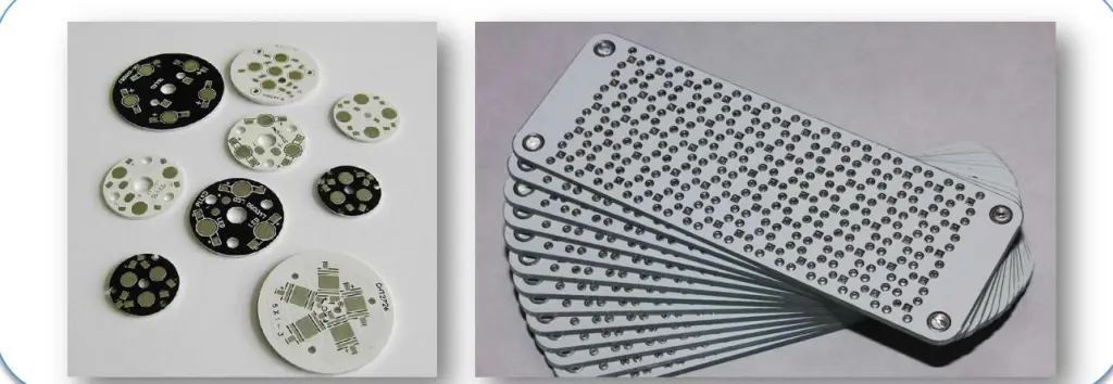
In recent years, the demand for aluminum PCBs has surged due to their numerous advantages over traditional FR4 PCBs. Aluminum PCBs are lightweight, highly conductive, and capable of withstanding high temperatures, making them ideal for applications in aerospace, automotive, LED lighting, and beyond.
This comprehensive guide will take you through the aluminum PCB manufacturing process step by step. We’ll explore the fabrication of single-layer, double-layer, and multilayer aluminum PCBs, providing a detailed look at how our engineers create these specialized boards. By the end, you’ll have a clear understanding of the entire process.
At RAYMING, we bring deep expertise in aluminum PCB manufacturing. Our state-of-the-art factory in China produces all types of aluminum PCBs, adhering to strict quality control and inspection protocols at every stage. With optimized fabrication techniques, we ensure high yields, fast turnaround times, and consistently flawless results.
Before diving into the manufacturing process, let’s understand what makes aluminum PCBs special.
What Are Aluminum PCBs?
Aluminum PCBs are circuit boards that use an aluminum base as the substrate instead of the traditional FR-4 material. This aluminum core provides excellent thermal conductivity, making these PCBs ideal for high-power applications.
As electronics continue to demand higher power and better thermal management, aluminum PCBs are set to play an increasingly important role. Their unique properties make them ideal for a wide range of applications, from everyday consumer electronics to cutting-edge industrial and military systems.
By understanding the aluminum PCB manufacturing process, designers and engineers can better leverage these innovative boards to create more efficient, powerful, and reliable electronic systems. As technology advances, we can expect to see even more applications benefiting from the unique properties of aluminum PCBs.
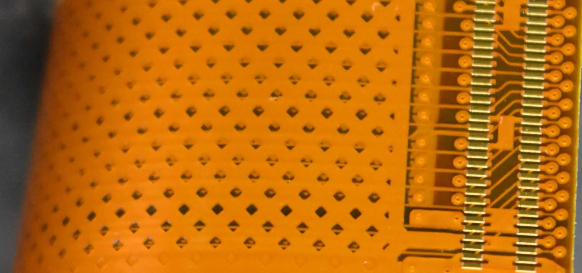
FPC circuit board is also called flexible circuit board, or “flexible board”. In the industry, FPC, is a printed circuit board made of flexible insulating substrate (mainly polyimide or polyester film), which has many advantages that hard printed circuit boards do not have. For example, it can bend, roll, fold, use FPC can greatly reduce the volume of electronic products, meet the needs of electronic products in the direction of high density, miniaturization, high reliability, therefore, FPC in space, military, mobile communications, Laptop computers, computer peripherals, PDA, digital cameras and other fields or products have been widely used.
FPC lamination process: lamination and opening die feeding / closed die prepressing / cooling / opening / cutting process ready TPX detached film\ steel\ silica gel and dust adhesive cloth or dusting paper to clean steel before the production of the following process: 1. Board\ silica\ off film surface dust, Sundries, etc. The size of the detached film (500m*500m) is opened and placed in the laminated area. After one cycle of each lamination, 400 pieces of spare steel plates are needed, so that the continuous production will not break the material. When laminating operation, you should wear gloves with both hands or fingers with 5 fingers.
It is strictly forbidden to touch soft plates with bare hands. D. When the plate is stacked, the steel plate is placed first. Keep this stack of 10 layers (except for special requirements), with the number of FPC placed on each layer to determine the number of pendulable FPC layers per 1PNL plate size (the distance from the plate to the four sides of the silica gel should be maintained above 7cm), The FPC should be placed in the middle of the silica gel as far as possible, and each plate should be spaced at a distance of 2 cm.
The thickness of the FPC should be consistent in each layer (for example, the single panel cannot be mixed with the multilayer pcb), and every opening and every layer of FPC should be the same. And the position and order of the pictures are roughly the same. When placing, the FPC coating surface or the paste reinforcement surface should be faced up, and the detached film should be flat and covered on the soft plate without wrinkling or folding. After the operation, the stacked FPC should be laid flat on the transport belt. To the next procedure.
With the aid of strict quality control and curing through the back stage, it has the characteristics of high temperature resistance, good separation effect and no pollution in the pressing process. The detached film can be supplied in the form of rolls and customized sizes to meet the different specifications of the customer and provide the appropriate and onlook-applied liquid pressure required to drive the laminate electronic components to the dense lamination. It eliminates air entering the bottom of the protective layer and between the circuit board.
2.TPX detached membrane
the effect is similar to that of the above type membrane, but some manufacturers of FPC circuit board have strict requirements. TPX detached film is a kind of high performance molecular material and can be used for all kinds of applications of high performance demoulding film. It is used as the main circuit board and cutting edge material of flexible printing substrate (FPC) by its excellent demembrane and heat resistance. Demoulded film for various occasions, with single-layer and multi-layer products, can be selected according to the use.
divided into red rubber pad and green rubber pad, it is a kind of synthetic elastic cushion made from silicone gel and polymer. The intermediate layer is glass fiber substrate, which greatly improves the strength and times of use of red silicone cushion. It has the characteristics of buffer, detachable, thermal equalization and so on. It is mainly used in hot pressing situations with high buffer requirement, such as: circuit board (FPC,PCB, soft and hard bonding board), solar energy, aerospace, power locomotive, die pressing, etc. Busbar compression and other fields.
5.The cushioning pad used repeatedly
it is developed and produced in accordance with the ultra-high temperature press used in the PCB industry at present. When the pressing temperature of the circuit board exceeds 260 ℃, the general auxiliary materials such as Kraft paper, cushioning pad and other auxiliary materials can no longer meet the high temperature pressing demand. Higher temperature resistant fibre must be used
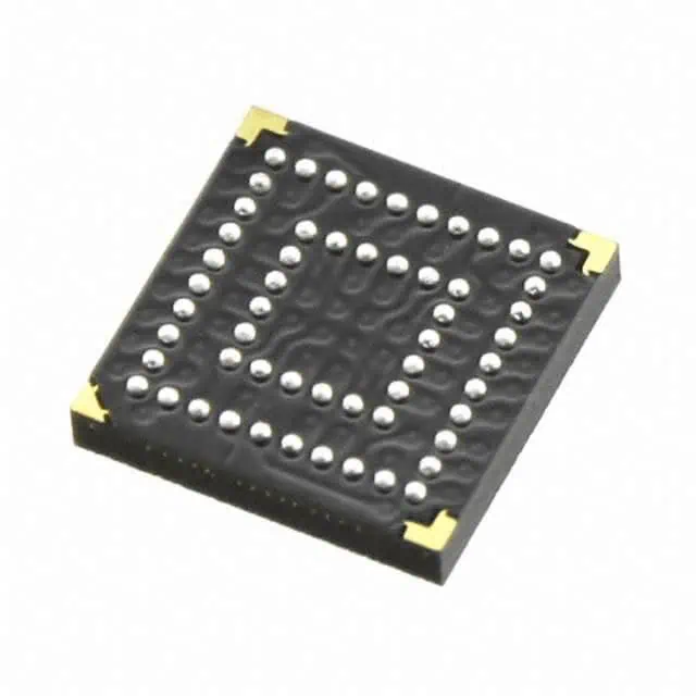
The Xilinx CoolRunner-II XCR3064XL-7PC44I is a low-power CPLD (complex programmable logic device) that provides medium density, performance, and an abundance of I/O in a compact form factor. The XCR3064XL balances logic capacity with low static and dynamic power consumption, making it an excellent fit for a wide variety of embedded applications.
In this article, we will take a technical deep dive into the capabilities, architecture, and key parameters of the XCR3064XL-7PC44I to understand where it excels and how to leverage its unique characteristics. We’ll explore the datasheet specifications and discuss example usage scenarios that can benefit from this CoolRunner-II device.
XCR3064XL Overview
Here are some of the high-level features of the Xilinx XCR3064XL-7PC44I CPLD:
A full embedded development toolchain enables CPLD-based designs with the XCR3064XL.
Conclusion
With its balanced density, ample performance, low power consumption, and abundance of I/O, the Xilinx XCR3064XL-7PC44I CPLD excels at a wide array of embedded system applications. The integrated development environment makes designing with the XCR3064XL accessible for new and experienced users alike. For embeddeed systems where a full FPGA may be overkill but a small CPLD lacks sufficient capacity, the XCR3064XL hits the sweet spot.
Frequently Asked Questions
Q: What are some typical applications suitable for the XCR3064XL CPLD?
A: Example uses including motor control, IoT edge nodes, industrial automation, algorithm accelerators, instrumentation, and interface glue logic.
Q: What density CPLD should be selected if the XCR3064XL does not have sufficient capacity?
A: The larger XC95108 and XC95144/216 CPLDs provide more macrocells and I/O for more complex designs.
Q: How does the XCR3064XL compare to competing CPLDs?
A: It competes with mid-density CPLDs from Lattice, Microsemi, and other vendors, but with lower power and cost.
Q: Does the XCR3064XL support in-system programming and reconfiguration?
A: Yes, via the JTAG interface the CPLD can be reprogrammed unlimited times on the PCB.
Q: What embedded processors work well with the XCR3064XL CPLD?
A: Simple 8-bit CPUs like Microchip PIC16/18, Atmel AVR, and TI MSP430 interface easily. 32-bit ARM cores can also leverage the CPLD.
XCR3064XL-7PC44I Description
The CoolRunner™ XPLA3 XCR3064XL device is a 3.3V, 64-macrocell CPLD targeted at power sensitive designs that require leading edge programmable logic solutions. A total of four function blocks provide 1,500 usable gates. Pin-to-pin propagation delays are as fast as 5.5 ns with a maximum system frequency of 192 MHz.
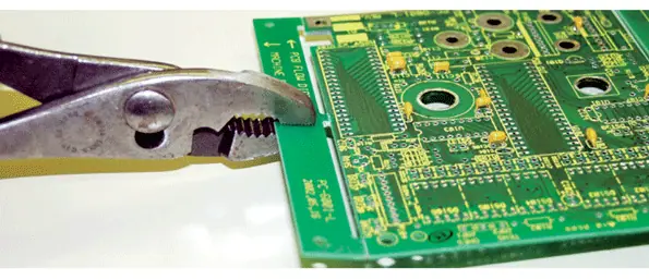
A PCB tab, also sometimes called a printed circuit board tab, refers to a simple rectangular extension of the PCB material beyond the edge of the circuit board. Tabs serve several functions in PCB design and manufacturing.
In this article, we’ll provide a full overview of PCB tabs including their purpose, typical dimensions, placement guidelines, and impact on fabrication and assembly processes. We’ll also describe alternatives to tabs and situations where minimal or no tabbing is recommended for optimal manufacturing results.
Functions of PCB Tabs
PCB tabs primarily serve two roles:
1. Maintaining Panel Stiffness
During fabrication, PCBs are produced in large panels consisting of multiple boards for efficiency. Tabs help keep these panels rigid through all processes. The small tabs bridge the spacing between boards. This retains stiffness that would be lost if boards were completely separated from each other.
Stiff panels prevent warping and damage during shipment and handling. Retained panel strength also allows easier loading and transfer through equipment.
2. Holding Boards in Panel
In addition to stiffness, tabs prevent individual PCBs shifting around or falling out of a panel prematurely before depaneling. Placement of tabs ensures each board remains fixed in its location within the panel matrix.
Tabs must be strong enough to withstand machine insertion forces and acceleration without tearing or releasing.
While tab parameters can vary between PCB fabricators, typical specifications are:
Width: 0.2” to 0.4” (5mm to 10mm)
Length: 0.4” to 1.2” (10mm to 30mm+)
Corner Radius: 0.06” (1.5mm)
Pattern: Repeating sets of tabs distributed along panel edges
This provides short, robust tabs able to withstand fabrication stresses while retaining board positioning and panel rigidity.
Longer or wider tabs increase strength but use up more board space. Smaller tabs save space but risk tearing during handling. Optimized tabbing balances both considerations.
PCB Panel Tabbing Guidelines
To function effectively, PCB panel tabs should follow certain design guidelines:
Place tabs at least every 3” to 5” (75mm to 125mm) along edges
Locate tabs at corners and vocational panel separation lines
Areas under high router forces require closer tab spacing
Radial tab sets help hold circular boards
Larger or thicker boards need bigger, stronger tabs
Match tab width to router blade width for cleanest cut
Tab placement is designed cooperatively between PCB designer and board fabrication house based on specific panel sizes, shapes, and equipment.
Alternatives to Full Tabbing
In some cases, full tabbing along all panel edges may not be beneficial or even feasible:
Low Tab Density
For simple boards with large spacing, minimal intermittent tabs maintain position without compromising stiffness.
Breakaway Tabs
Rather than rectangular tabs, thin fracturable tabs or score lines work as break points.
Tooling Holes
Round tooling holes used in combination with partial tabs secure panel alignment.
No Tabs
Some panel and board sizes ship successfully without tabbing. Reduces fabrication work.
Specialty Shielding
For metal shielded boards, plated tabs may short shielding. Insulating sections or adhesives are used.
Router passes slice tabs precisely without tearing or leaving burrs on boards.
Masking
Liquid photoimageable solder mask must coat tab edges without bridging between boards.
Testing
Fixture contacts avoid tabs during in-circuit testing. Ground tabs may impact probing.
Assembly
Components avoid tabs. Tabs considered in pick and place programs.
Depaneling PCBs
Most often tabs get removed along with the rest of the panel remnants during PCB depaneling:
Tab Rout
A final routing pass slices tabs flush with board edges in one action.
Tab Punch
Pneumatic punch dies cleanly snap off tabs leaving smooth board edges.
Break Tabs
Operators manually snap off thin breakaway tabs after routing.
Leave Tabs
Some applications incorporate tabs as part of board, removing unneeded ones.
Depending on tab design, automated or manual depaneling removes tabs after all fabrication and assembly work is complete.
Conclusion
PCB tabs are simple but serve an important role in panelization and fabrication. Appropriately engineering tabs improves manufacturing yield and quality while minimizing space and cost impacts. When designed well in consultation with PCB fabricators, tabs become an indispensable part of efficient panelized board production.
Frequently Asked Questions
Q: What are typical PCB tab thickness?
A: Tabs use the same laminate and thickness as the rest of the boards in a panel. This ranges from 0.005” to 0.125” typically.
The article introduces a simple design principle of removing PCBA break away tab. This design can quickly and reliably cut PCB boards of various sizes and pre-engraved with V-grooves. Hope it can help engineering designers.
The development background
PCBA refers to PCB that have been assembled with electronic components and are widely used in various fields such as aviation, numerical control, computers, and automation instruments.
Due to manufacturing and logistics requirements, the edge of the prototype pcb assembly board needs to be reserved, which is not required for the product side. Therefore, the PCBA break away tab needs to be removed after the components are assembled.
The method of removing the PCBA break away tab can be divided into three categories: V-cut depanelizer, milling depanelizer, and manually.
The milling depanelizer has the best function, which overcomes the limitation that the V-cut can only be linearly divided. The high-speed operation of the milling cutter is used to separate the multiple-connected PCBA according to the pre-programmed path, which improve product quality and reduce scrap rate. The disadvantage is that it is very expensive and cumbersome to operate (programming required).
The price of the V-cut depanelizer is much cheaper. It is cut along the PCBA V-groove by the blade, but it can only be cut straight, and the cost of the blade is expensive.
3.Manually removing the break away tab is by hand or needle-nosed pliers and other tools for segmentation, with low cost and easy to use, but it is also easy to damage components.
For small batches, multiple varieties and low cost manufacturing requirements, manually removing break away tab is most practical. But for big batches PCBA orders, how could we remove the PCBA break away tab? In order to solve these problems, we have developed a simple tool for manual removal of the PCBA break away tab.
The tooling achieves the purpose of removing the break away tab through a simple mechanical structure, with low cost, which can meet the requirements of adapting to different sizes and thicknesses of the process side.
he tooling adopts the following technical solution: an adjustable auxiliary device for manually removing the PCBA break away tab side, including a mounting base plate, a slider base, a movable slider, an adjustment button, and a transmission structure.
The movable slider is driven to move along the set track on the base of the slider by manually adjusting the adjustment button. After a suitable distance, the process edge to be removed from the PCBA board is placed in the card slot of the device, and finally the PCBA board is held by both hands. The function of manually removing the edge of the process can be realized by gently applying force in one direction below. Please refer to he specific working principle as below picture.
It should be noted that the hands should not be gripped on the top of the PCBA, which is the most labor-saving from the perspective of the principle of the lever, but the stress is also the largest, which is easy to damage the PCBA.
As a preferred embodiment, the mounting bottom plate of the tooling may be a workbench, or other forms of work surface, not limited to the form of the bottom plate; the slider base and the movable sliding block may be a linear bayonet dovetail groove or other The movement fit and the structural form are not limited to various types of movable fits and structural forms; the adjustment buttons may be manual rotation adjustments or other forms of adjustment buttons, not limited to the form of adjustment buttons; the transmission structure may be a cone Gear transmissions or other forms of transmission structure are not limited to the structural form of the transmission.
Compared with the prior art, the tooling has the following advantages:
(1) Low production costs;
(2) Simple operation;
(3) The quality of the process edge is good, and the components on the PCBA board are under stress;
(4) It has a wide application range and can adapt to PCBA boards with different thicknesses and board margins;
(5) The structure is flexible and convenient, and the PCBA board can be manually adjusted to adapt to various thickness and size process sides.
Conclusion
The application of the new manual removal of the PCBA break away tab side auxiliary device not only takes into account the stress control requirements of the PCBA when removing the process side, but also takes into account the cost control of the production. In this way, the tooling can replace the high-cost special equipment, so it is an auxiliary device that is practical, flexible, and can reduce the overall cost, and can be widely used.
Pseudo soldering is a defect that can occur during PCB assembly, resulting in poor solder joint reliability. It happens when the solder paste or component termination oxidizes during reflow, preventing proper wetting and adhesion. This leads to weakened interconnections prone to failure under thermal cycling or vibration.
This article explores the root causes of pseudo soldering, how to recognize it, and proven methods to avoid the problem. By understanding what conditions induce pseudo soldering and implementing countermeasures, robust solder joints can be ensured. Preventing pseudo soldering during manufacturing results in electronic products with enhanced durability.
What is Pseudo Soldering?
Pseudo soldering describes solder joints that exhibit poor wetting characteristic despite appearing shiny and properly formed after assembly. The term “pseudo soldering” comes from joints that mimic properly soldered connections visually, but lack reliable adhesion and bonding.
Pseudo soldered joints often function initially but degrade and fail rapidly under temperature cycling or mechanical shock and vibration. This delayed onset of field failures makes pseudo soldering notoriously difficult to detect through standard quality inspections.
Pseudo soldering arises from factors that prevent molten solder from adequately wetting and adhering to PCB pad and component lead surfaces during reflow. Major causes include:
Oxidation – Formation of oxides on solderable surfaces inhibits wetting. Common with no-clean solder pastes.
Contamination – Organic residues or chemicals on pads or leads blocks solder flow.
Insufficient Flux – Not enough flux activation leads to imperfect wetting.
Excess Reflow Time – Extended high temperature exposure burns off flux prior to soldering.
Poor Metal Finishes – Refractory leads or pads resist solder alloy bonding.
Any condition that hampers free flowing and joining of liquid solder metal to board and component surfaces can initiate pseudo soldering defects.
Impact of Solder Paste Oxidation
A major driver of pseudo soldering is excessive oxidation of solder powder within paste during the reflow process. Solder powder forms an initial oxide layer when manufactured that must be broken during soldering for proper wetting.
However, prolonged reflow exposure grows this oxide layer too thick to penetrate. Factors inducing excessive solder paste oxidation include:
High reflow peak temperatures
Extended reflow duration above liquidus
Multiple reflow passes
Delayed reflow after paste application
Low activity flux unable to reduce oxides
Porous solder powder with higher surface area
Any increase in oxidation leads directly to reduced solderability and pseudo soldering risk.
Effect of Lead-Free Solder Alloys
Lead-free solders are particularly susceptible to pseudo soldering versus traditional tin-lead alloys:
Higher reflow temperatures grow thicker oxides
Require more aggressive flux to fully activate solder
Less forgiving of marginal soldering processes
Common SAC alloys more prone to oxidation than tin-lead
The reduced solderability of lead-free alloys places greater importance on minimizing oxidation and following robust processes to prevent pseudo soldering issues.
This results in intermittent faults or total product failures after minimal time in service. Such extremely poor reliability makes prevention in manufacturing critical.
Automated optical inspection (AOI) for non-wetting
Elevated temperature electrical resistance testing
Because pseudo soldering forms inside joints, destructive and electrical testing provides the most definitive detection. But this requires examination of samples outside of production.
Solutions to Avoid Pseudo Soldering
Minimizing the risk of unstable solder joints requires steps throughout the manufacturing process:
Solder Paste Selection
Match alloy to pad metallizations
Select very high activity/low residue flux
Use solder powder with less surface area
Reflow Profile Optimization
Lower peak temperature if possible
Shorten time above liquidus
Ramp down rapidly after reflow
Surface Preparation
Thorough cleaning of pads and leads
Remove all surface residues
Apply liquid flux to pads and leads
Reflow Environment
Prevent excessive oxygen exposure
Use nitrogen reflow environment
Joint inspection, analysis, and testing provides feedback to refine the process.
Pseudo soldering continues to trouble lead-free soldering processes. By understanding the causes and implementing countermeasures, the risk of latent solder joint failures can be greatly reduced. Careful optimization of solder paste, reflow profile, surface preparation, and the reflow environment allows excellent solderability and long-term reliability for electronics.
Frequently Asked Questions
Q: How can you visually identify a pseudo soldered joint?
A: Pseudo soldered joints appear shiny and properly formed initially. Only destructive testing or microscopy on cross-sections reveals internal voids or cracks over time.
Q: What are some example lead-free solder alloy options less prone to oxidation?
A: Low silver SAC alloys, bismuth alloys, and solder formulations incorporating dopants for oxidation resistance can provide improved solderability.
Q: Should extra liquid flux always be applied when soldering with no-clean solder paste?
A: Additional flux provides further activation but risks leaving difficult to clean residues. It should only be used selectively when needed.
Q: What causes solder balling defects and how does it relate to pseudo soldering?
A: Insufficient wetting allows solder to ball up on pads. Both conditions share root causes of oxidation and inadequate flux activity.
Q: How can you include testing for pseudo soldering failures during product qualification?
A: Examining samples after accelerated temperature cycling, drop testing, and vibration will reveal any latent solder joint defects present.
The Causes And Solutions Of PCBA Pseudo Soldering
PCBApseudo soldering is also known as cold soldering. The surface seems to be soldered, but the actual internals are not connected, or the intermediate unstable state that may or may not pass, affecting the circuit characteristics, may cause the PCB board quality to be unqualified. Or scrapped. Therefore, we must pay attention to the phenomenon of PCBA pseudo soldering. ShenZhen Rayming Electronics is a professional PCBA processing factory with rich experience in PCBA production and processing. Here are the reasons and solutions for PCBA soldering.
First, PCBA pseudo soldering joint is a common type of circuit fault. The causes of solder joint are common in the following two types:
In the process of PCBA chip processing, due to improper production process, such as poor soldering or less tin, the component legs and pads are not turned on, etc., and the circuit board is in an unstable state when circuit is turn on and turn off sometimes;
Due to the long-term use of electrical appliances, some parts with more serious heat generation are prone to aging peeling or the presence of impurities due to the solder joints at the solder joints.
Second, determine the PCBA solder joint location method:
Judging the approximate fault range according to the fault phenomenon that occurs;
Appearance observation, focusing on the larger components and components with large heat generation;
Use a magnifying glass for observation;
Shake the suspicious component by hand and observe if the solder joints on the pins are loose.
Third, the method of solving PCBA pseudo soldering:
In the PCBA processing process, the pseudo soldering is an important reason that affects the quality of the circuit board. Once the pseudo soldering phenomenon occurs, it needs to be reworked, which not only increases the labor pressure, but also reduces the production efficiency and causes losses to the enterprise. Therefore, it is necessary to avoid the cold soldering. The phenomenon is generated, the inspection work is done, and once the pseudo soldering occurs, it is necessary to find the cause and solve it immediately.
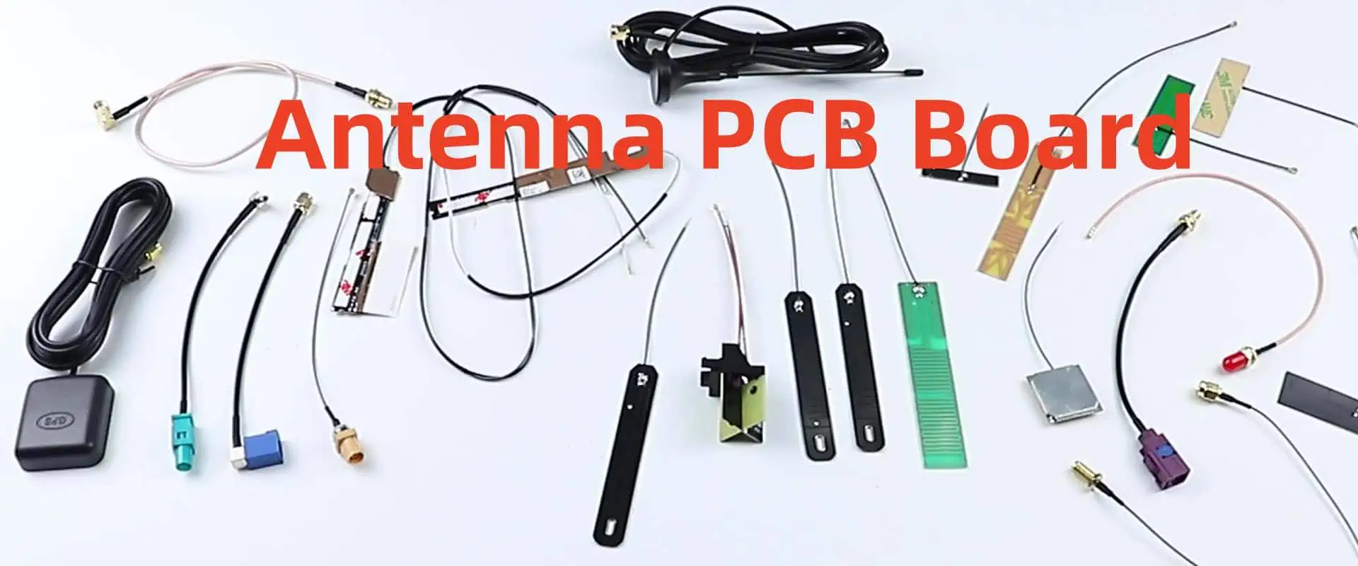
A wide variety of antennas are available as off-the-shelf components, making them a convenient choice for engineers designing systems that require wireless communication. However, antennas used in PCBs can also be printed directly onto the board, enabling fully customized designs and unique architectures that integrate seamlessly into a single assembly. Additionally, PCB-mounted antennas, such as chip antennas or System-on-Chip (SoC) modules with integrated radios, may require either an antenna module or an off-the-shelf component to function effectively.
Whether the antenna is printed directly onto the PCB or sourced as a pre-made component, it is crucial for PCB designers to have a deep understanding of how antennas operate. Experienced designers will recognize that a PCB itself contains numerous elements that can unintentionally act as efficient antennas. In this article, we will explore some of the fundamental concepts behind antennas, providing engineers with the knowledge needed to design, select, and position antennas effectively in their projects.
What is PCB Antenna?
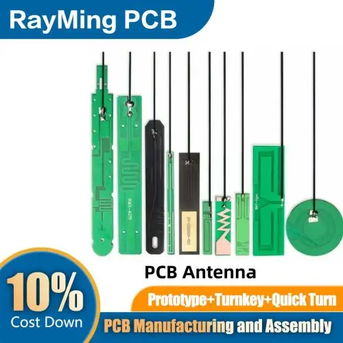
A PCB antenna, short for Printed Circuit Board antenna, is a type of antenna fabricated directly onto a printed circuit board. Unlike traditional antennas that are separate components, PCB antennas are integrated into the circuit board itself, making them an integral part of the device’s overall design.
PCB antennas offer several advantages:
Cost-effective: They eliminate the need for separate antenna components, reducing overall production costs.
Space-saving: PCB antennas are ideal for compact devices where space is at a premium.
Consistency: Being part of the PCB ensures consistent performance across manufactured units.
Durability: Integrated into the board, these antennas are less prone to damage from external factors.
Antenna PCB Calculator
RayPCB Engineering Tools
Rectangular Patch Antenna Calculator
Calculated Dimensions
Patch Width (W)--
Patch Length (L)--
Effective εr--
Feed Point (from edge)--
Ground Plane (min)--
Visual Reference
W × L Patch
WLh
--
Wavelength (λ₀)
--
Est. Bandwidth
--
Est. Gain
W = c / (2f₀) × √(2/(εr+1))
L = c / (2f₀√εeff) - 2ΔL
ΔL = 0.412h × (εeff+0.3)(W/h+0.264) / (εeff-0.258)(W/h+0.8)
Design Tip
For optimal bandwidth, substrate height should be 0.003λ₀ to 0.05λ₀. Thicker substrates increase bandwidth but may excite surface waves. Rogers RO4003C offers excellent performance for most antenna applications with good thermal stability.
Microstrip Line Calculator
Microstrip Parameters
Trace Width--
Effective εr--
λ/4 Length--
λ/2 Length--
W/h Ratio--
Quarter-Wave Transformer
Transformer Parameters
Required Z₀--
λ/4 Length--
RF/Microwave Substrate Materials Database
Rogers RO4003C
Dielectric (εr)3.55 ±0.05
Loss Tangent0.0027
Tg>280°C
Best ForGeneral RF
Rogers RO4350B
Dielectric (εr)3.38 ±0.05
Loss Tangent0.0037
Tg>280°C
Best ForUHF-Microwave
Rogers RT/duroid 5880
Dielectric (εr)2.2 ±0.02
Loss Tangent0.0009
TgN/A (PTFE)
Best FormmWave
Rogers RO3003
Dielectric (εr)3.0 ±0.04
Loss Tangent0.0013
TgN/A
Best ForPhased Arrays
FR-4 Standard
Dielectric (εr)4.2-4.6
Loss Tangent0.02
Tg130-140°C
Best For<2 GHz
Rogers RO3006
Dielectric (εr)6.15 ±0.15
Loss Tangent0.0025
TgN/A
Best ForSize Reduction
High-Tg FR-4
Dielectric (εr)4.2 ±0.2
Loss Tangent0.015
Tg170°C
Best ForBudget RF
Rogers RO3010
Dielectric (εr)10.2 ±0.3
Loss Tangent0.0023
TgN/A
Best ForMiniaturization
Material Selection Guide
Choose Rogers RO4003C or RO4350B for general antenna applications up to 10 GHz. For mmWave (>24 GHz), use RT/duroid 5880 or similar PTFE materials. FR-4 is suitable only for sub-2 GHz applications where cost is critical.
For antenna PCBs, place the antenna on the top layer with an uninterrupted ground plane on L2. Keep digital signals away from RF sections. Use via stitching around antenna edges to suppress surface waves and improve isolation.
Antenna PCB Manufacturing Guidelines
Use controlled impedance fabrication for all RF traces (±10% tolerance)
Specify ENIG or OSP surface finish for antenna elements (avoid HASL)
Request solder mask opening over antenna patch elements
Minimum 6x substrate height for ground plane extension
Via stitching spacing ≤ λ/20 around antenna perimeter
Keep digital components minimum λ/4 away from antenna
Use coplanar waveguide or microstrip for RF feed lines
Add test points for VNA measurements (50Ω SMA pad)
Surface Finish Comparison
Finish
RF Suitability
Shelf Life
Cost
ENIG
Excellent
12+ months
$$$
OSP
Very Good
6 months
$
Immersion Tin
Good
6 months
$$
HASL
Poor
12 months
$
Immersion Silver
Excellent
6 months
$$
Tolerance Specifications
Parameter
Standard
RF Grade
Trace Width
±20%
±10%
Dielectric Thickness
±10%
±5%
Impedance
±15%
±5%
Registration
±100 μm
±50 μm
Copper Thickness
±20%
±10%
RayPCB Manufacturing Support
RayPCB offers specialized antenna PCB manufacturing with Rogers materials, controlled impedance, and RF testing capabilities. Contact our engineering team for design review and DFM analysis of your antenna designs.
PCB antennas function based on the same principles as traditional antennas. They are designed to transmit and receive electromagnetic waves at specific frequencies. The key difference lies in their construction and integration with the circuit board.
Here’s a brief overview of how PCB antennas work:
Signal Generation: The device’s circuitry generates an electrical signal.
Conversion: The antenna converts this electrical signal into electromagnetic waves for transmission.
Radiation: The electromagnetic waves are radiated into the surrounding space.
Reception: For incoming signals, the process is reversed. The antenna captures electromagnetic waves and converts them back into electrical signals.
The specific design of the PCB antenna, including its shape, size, and placement on the board, determines its frequency range, radiation pattern, and overall performance.
Types of PCB Antennas
There are various types of PCB antennas, each with its unique characteristics and applications. Let’s explore some of the most common types:
1. PCB Monopole Antenna
The PCB monopole antenna is one of the simplest and most widely used designs. It consists of a single conductive element, typically a straight trace on the PCB, with a ground plane.
Key features:
Simple design
Omnidirectional radiation pattern
Suitable for a wide range of frequencies
Commonly used in mobile devices and IoT applications
2. PCB Dipole Antenna
A PCB dipole antenna consists of two identical conductive elements, often arranged in a straight line. Unlike the monopole, it doesn’t require a ground plane.
Key features:
Balanced design
Bi-directional radiation pattern
Good performance in free space
Used in RFID tags and wireless sensors
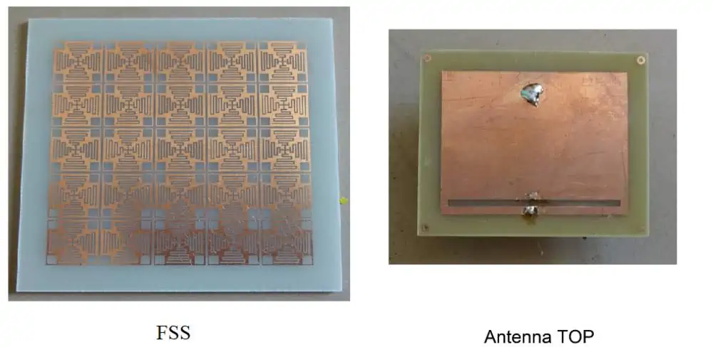
3. PCB Patch Antenna
Also known as a microstrip antenna, the PCB patch antenna consists of a flat rectangular sheet or “patch” of metal on top of a larger sheet of metal (ground plane) separated by a dielectric substrate.
Key features:
Low profile and lightweight
Directional radiation pattern
High gain
Commonly used in GPS receivers and satellite communications
4. PCB Loop Antenna
PCB Loop Antenna
PCB loop antennas are formed by creating a loop of conductive material on the PCB. They can be circular, square, or other shapes.
Key features:
Compact size
Good performance in near-field applications
Often used in NFC and RFID systems
Suitable for low-frequency applications
5. PCB Helical Antenna
A PCB helical antenna is created by forming a helical pattern on the PCB. It’s essentially a three-dimensional structure created on a two-dimensional surface.
Key features:
Circular polarization
High gain
Narrow beamwidth
Used in satellite communications and GPS applications
6. PCB Slot Antenna
PCB slot antennas are created by cutting a slot in the ground plane of the PCB. The slot acts as the radiating element.
Key features:
Low profile
Can be integrated into existing ground planes
Bidirectional radiation pattern
Used in mobile devices and aircraft communications
7. PCB Yagi Antenna
Yagi Antenna PCB
A PCB Yagi antenna, also known as a Yagi-Uda antenna, consists of multiple elements including a driven element, reflector, and one or more directors.
Key features:
High directivity
High gain
Used for point-to-point communications
Common in TV antennas and long-range Wi-Fi
8. Planar Inverted F Antenna (PIFA)
The PIFA is a variation of the monopole antenna, with the top section folded down to be parallel with the ground plane.
Key features:
Compact size
Good performance close to the human body
Widely used in mobile phones
Can be easily integrated into handheld devices
9. Meander Line Antenna
A meander line antenna is created by forming a meandering pattern on the PCB, effectively increasing the electrical length of the antenna while maintaining a compact physical size.
Key features:
Very compact design
Suitable for low-frequency applications in small devices
Can be implemented in various shapes (meandered, spiral, etc.)
Used in low-cost devices and RFID tags
What are the Best Materials for Circuits with Antennas?
Choosing the right materials for PCB antennas is crucial for optimal performance. The key factors to consider are the dielectric constant (εr) and the loss tangent of the substrate material. Here are some commonly used materials:
FR-4: A popular and cost-effective choice for many applications. It has a dielectric constant of about 4.4 and is suitable for frequencies up to about 1 GHz.
Rogers RO4350B: This material offers lower loss and better performance at high frequencies compared to FR-4. It’s often used for antennas operating above 1 GHz.
Taconic RF-35: Another high-performance material with low loss, suitable for high-frequency applications.
PTFE (Teflon): PTFE-based materials offer very low loss and are excellent for high-frequency and high-performance applications. However, they are more expensive and harder to process.
Ceramic-filled PTFE composites: These materials offer a good balance between performance and processability.
The choice of material depends on the specific requirements of the antenna, including frequency range, performance needs, and cost constraints.
Choosing an Antenna
Selecting the right antenna for your application involves considering several factors:
Frequency Range: The antenna must be designed for the specific frequency or range of frequencies required by your application.
Size Constraints: The available space in your device will influence the type and size of antenna you can use.
Radiation Pattern: Different applications require different radiation patterns. For example, a mobile phone might need an omnidirectional pattern, while a satellite dish needs a highly directional pattern.
Gain and Efficiency: Higher gain antennas can transmit and receive signals over longer distances but may have more directional radiation patterns.
Environmental Factors: Consider the environment in which the antenna will operate, including proximity to other components, potential interference sources, and physical conditions.
Cost: Some antenna designs are more complex and expensive to manufacture than others.
Regulatory Compliance: Ensure that your chosen antenna meets all relevant regulatory requirements for your target markets.
Antenna Design Principles for PCB Designers
Designing effective PCB antennas requires a good understanding of RF principles and careful consideration of various factors. Here are some key principles to keep in mind:
Impedance Matching: The antenna should be matched to the impedance of the feed line (typically 50 ohms) to maximize power transfer and minimize reflections.
Ground Plane Considerations: Many PCB antennas require a ground plane. The size and shape of this ground plane can significantly affect antenna performance.
Trace Width and Spacing: The width of PCB traces and their spacing from other traces and ground planes can affect the antenna’s characteristics.
Antenna Placement: The location of the antenna on the PCB can impact its performance. Keep it away from noise sources and consider the effects of nearby components.
Use of Vias: Vias can be used to create connections between layers and to implement certain antenna designs, but their placement must be carefully considered.
Simulation and Modeling: Use electromagnetic simulation tools to model and optimize your antenna design before fabrication.
Prototyping and Testing: Always prototype and test your antenna designs to verify their performance in real-world conditions.
Performance Testing and Optimization
Once a PCB antenna is designed and fabricated, it’s crucial to test its performance and optimize it if necessary. Here are some key aspects of antenna testing and optimization:
S-Parameter Measurements: Use a vector network analyzer to measure S-parameters, particularly S11 (return loss), which indicates how well the antenna is matched to its feed line.
VSWR Measurement: The Voltage Standing Wave Ratio is another measure of impedance matching.
Radiation Pattern Measurement: This shows how the antenna radiates energy in different directions.
Gain Measurement: Determine the antenna’s gain, which indicates how well it concentrates energy in a particular direction.
Efficiency Measurement: This indicates how much of the input power is actually radiated by the antenna.
Bandwidth Measurement: Verify that the antenna performs well across its intended frequency range.
Near-Field Scanning: This can help identify areas of high field strength on the PCB, which can be useful for EMC considerations.
After testing, optimization might involve:
Adjusting the antenna’s dimensions
Modifying the matching network
Changing the antenna’s position on the board
Altering the ground plane design
Using different PCB materials
Iterative testing and optimization are often necessary to achieve the best possible performance.
PCB Antenna vs. Chip Antenna
When designing an RF system, engineers often need to choose between PCB antennas and chip antennas. Here’s a comparison of the two:
PCB Antenna
Advantages:
Lower cost, especially in high volumes
Can be customized for specific applications
No additional components required
Can achieve better performance in some cases
Disadvantages:
Requires more PCB space
Performance can be affected by other components and PCB layout
May require more design and optimization time
Chip Antenna
Advantages:
Very compact size
Consistent performance across different devices
Easier to implement, especially for inexperienced designers
Less affected by nearby components
Disadvantages:
Higher component cost
Limited customization options
May have lower performance compared to well-designed PCB antennas
Requires a specific ground plane size for optimal performance
The choice between PCB and chip antennas depends on factors such as available space, design expertise, production volume, and performance requirements. In many cases, PCB antennas offer a good balance of cost, performance, and flexibility, making them a popular choice for many applications.
Conclusion
Antenna PCB technology has revolutionized the world of wireless communication, enabling the creation of compact, efficient, and cost-effective devices. From simple monopole designs to complex MIMO systems, PCB antennas offer a wide range of solutions for various applications.
As an RF engineer, understanding the principles of PCB antenna design, the characteristics of different antenna types, and the factors that influence antenna performance is crucial. By carefully considering these aspects and following best practices in design, testing, and optimization, you can create PCB antennas that meet the demanding requirements of modern wireless systems.
As technology continues to evolve, PCB antennas will undoubtedly play an increasingly important role in shaping the future of wireless communication. Whether you’re working on IoT devices, mobile phones, satellite systems, or any other wireless application, mastering the art and science of PCB antenna design will be a valuable skill in your RF engineering toolkit.
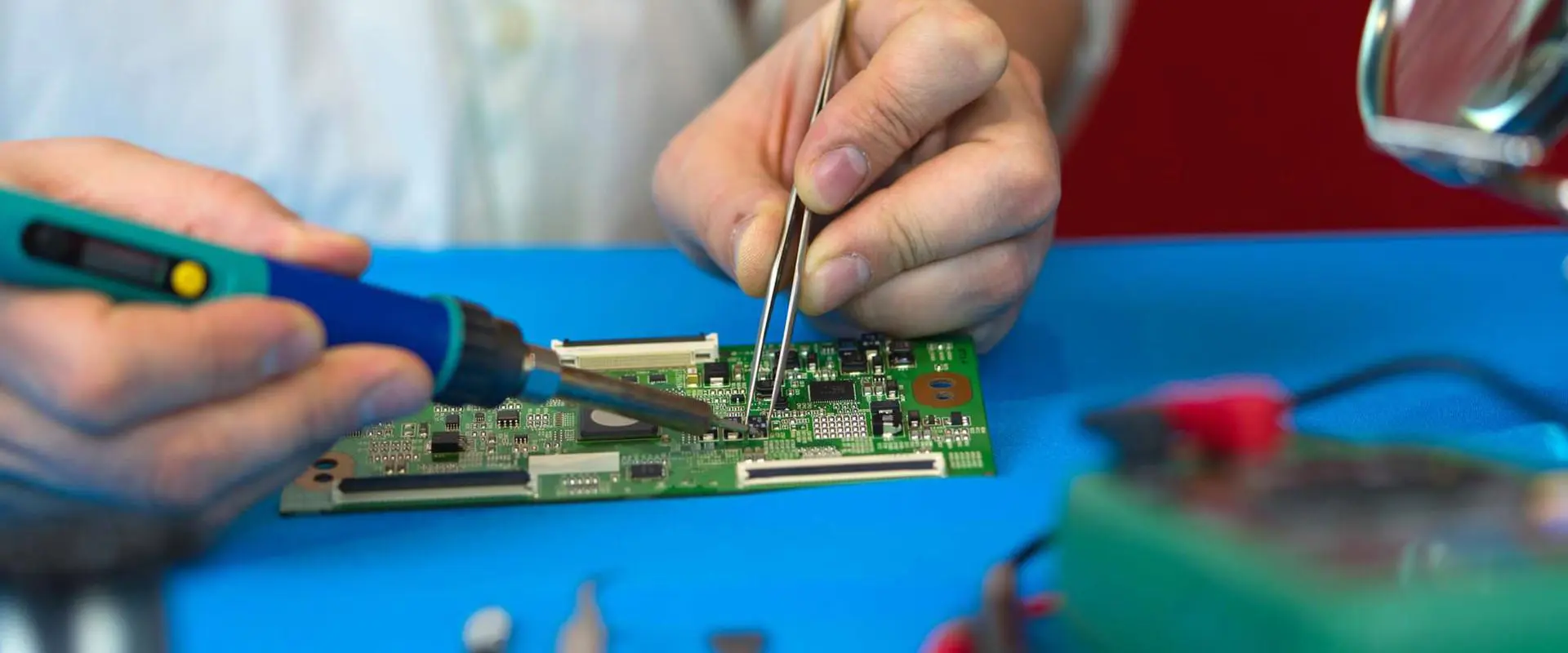
PCB soldering is a fundamental skill in electronics manufacturing and repair. Whether you’re a hobbyist working on a DIY project or a professional in the electronics industry, mastering PCB soldering techniques is crucial for creating reliable and high-quality electronic devices. In this comprehensive guide, we’ll explore the essentials of PCB soldering, from basic concepts to advanced techniques, and highlight common mistakes to avoid.
What is PCB Soldering?
PCB soldering is the process of joining electronic components to a printed circuit board (PCB) using a metal alloy called solder. This process creates both an electrical connection and a mechanical bond, ensuring that the components stay in place and function properly within the circuit.
The Importance of Proper PCB Soldering
Proper PCB soldering is critical for several reasons:
Electrical Conductivity: Good solder joints ensure optimal electrical connections between components and the PCB.
Mechanical Strength: Well-soldered joints provide physical stability, preventing components from detaching due to vibration or mechanical stress.
Reliability: Properly soldered connections are less likely to fail over time, increasing the overall reliability of the electronic device.
Performance: Poor soldering can lead to issues like signal noise, voltage drops, and intermittent connections, all of which can affect device performance.
Equipment and Materials for Soldering
To perform PCB soldering effectively, you’ll need the right tools and materials. Here’s a list of essential equipment:
Soldering Iron
The soldering iron is your primary tool. Look for these features:
Temperature control
Interchangeable tips
Comfortable grip
Adequate power (typically 20-60 watts for most PCB work)
Solder
Choose the right type of solder for your project:
Lead-based solder (60/40 or 63/37 tin-lead alloys)
Lead-free solder (typically containing tin, copper, and silver)
Flux
Flux helps improve solder flow and removes oxides. Options include:
Let’s walk through the process of manually soldering a through-hole component to a PCB.
1. Tin the Soldering Iron
Clean the tip of your soldering iron
Apply a small amount of solder to the tip
This process, called “tinning,” improves heat transfer
2. Prepare the PCB Surface
Ensure the PCB is clean and free from contaminants
If necessary, use isopropyl alcohol to clean the board
3. Position Your Components
Insert the component leads through the appropriate holes
If working on the component side, bend the leads slightly to hold the component in place
4. Heat the Joint
Place the soldering iron tip so it contacts both the pad and the component lead
Hold for 2-3 seconds to heat both surfaces
5. Solder the Joint
Apply solder to the joint, not the iron tip
The solder should flow smoothly, forming a concave fillet
Remove the solder, then the iron
6. Inspect the Joint and Trim the Leads
Check for a smooth, shiny solder joint
Trim excess lead length with flush cutters
13 Types of PCB Soldering Defects and Solutions
Even experienced technicians can encounter soldering defects. Here are 13 common issues and how to address them:
1. Bridging of Solder
Problem: Solder connects two points that should be separate. Solution: Use a smaller soldering tip, apply less solder, or use solder wick to remove excess.
2. Excess of Solder
Problem: Too much solder on a joint, forming a ball or blob. Solution: Remove excess with solder wick or a desoldering pump.
3. Balling of Solder
Problem: Small balls of solder scatter around the work area. Solution: Clean the area, use flux, and ensure proper heating of the joint.
4. Heat Loss Analysis
Problem: Insufficient heat transfer to form a good joint. Solution: Use a higher wattage iron or increase temperature settings.
5. Tombstoning
Problem: One end of a surface-mount component lifts off the board. Solution: Ensure even heating and proper solder paste application.
6. Pins and Connector Connections
Problem: Poor connections on multi-pin components. Solution: Use appropriate flux, ensure proper heating, and consider using a hot air rework station.
7. Surface Mount Issues
Problem: Misalignment or poor connections on SMD components. Solution: Use a stencil for solder paste application, and consider using a reflow oven or hot air station.
8. Skipped Solder
Problem: Solder fails to wet a pad or lead. Solution: Clean the surfaces, use flux, and ensure proper heating.
9. Lifted Pads
Problem: Copper pad separates from the PCB. Solution: Avoid overheating, use proper technique, and consider board repair if necessary.
10. Pinholes and Blowholes
Problem: Small holes or voids in the solder joint. Solution: Ensure proper flux application and adjust soldering temperature.
11. Chemical Flow Issues
Problem: Improper flux activation or cleaning. Solution: Use the correct type of flux and follow proper cleaning procedures.
12. Faulty Wire Breakage
Problem: Wires break at the solder joint due to stress. Solution: Use strain relief techniques and avoid overheating insulation.
13. Insufficient Heat
Problem: Cold solder joints due to inadequate heating. Solution: Increase iron temperature, use a larger tip, or heat the joint for a longer time.
How to Get Soldering Training
Improving your soldering skills is an ongoing process. Here are some ways to get training:
Online Courses: Platforms like Coursera, Udemy, and SkillShare offer soldering courses.
Local Workshops: Check with community colleges or maker spaces for hands-on classes.
Manufacturer Training: Some equipment manufacturers offer training programs.
Certification Programs: Organizations like IPC offer professional certification in soldering.
Practice Projects: Start with simple kits and gradually tackle more complex projects.
Quick Tips and Tricks for Soldering
To wrap up, here are some valuable tips to improve your soldering technique:
Keep It Clean: Regularly clean your soldering iron tip and work area.
Use Flux: Flux improves solder flow and joint quality.
Temperature Matters: Use the correct temperature for your solder type and components.
Steady Hands: Use helping hands or PCB holders to keep your work steady.
Inspect Your Work: Use magnification to check your joints regularly.
Practice Heat Control: Learn to apply heat quickly and efficiently.
Choose the Right Tip: Different tip shapes suit different tasks.
Avoid Breathing Fumes: Use a fume extractor to protect your health.
Learn to Read Joints: Develop an eye for identifying good and bad solder joints.
Stay Updated: Keep learning about new techniques and technologies in PCB assembly.
Conclusion
PCB soldering is a critical skill in electronics manufacturing and repair. By understanding the fundamentals, using the right tools and techniques, and being aware of common defects, you can significantly improve the quality and reliability of your electronic assemblies. Remember that mastering PCB soldering takes time and practice, so don’t be discouraged if you encounter challenges along the way. Keep refining your skills, stay curious, and always prioritize quality in your work.
Whether you’re a hobbyist working on DIY projects or a professional in the electronics industry, the principles and techniques covered in this guide will help you achieve better results in your PCB soldering endeavors. As electronics continue to evolve, with components becoming smaller and more complex, your soldering skills will become increasingly valuable. Embrace the learning process, and you’ll be well-equipped to tackle even the most challenging PCB assembly tasks.
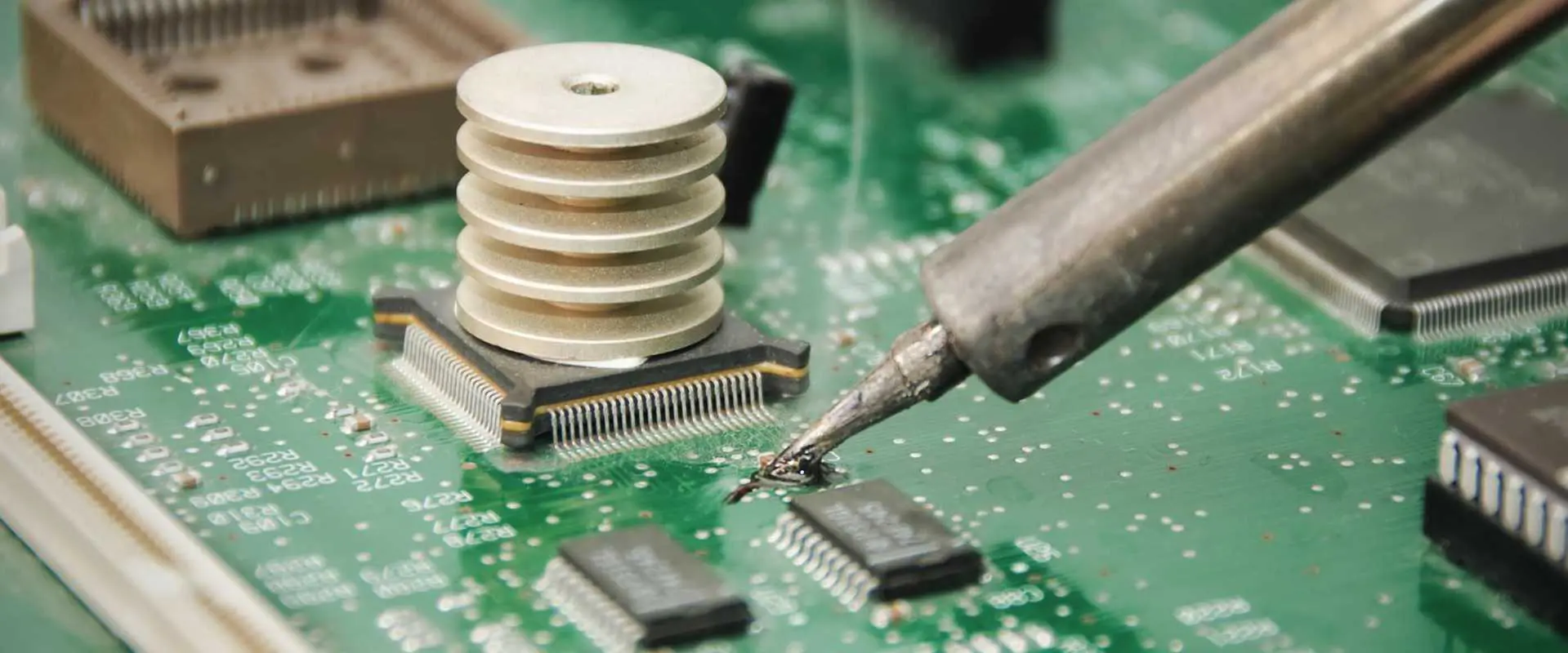
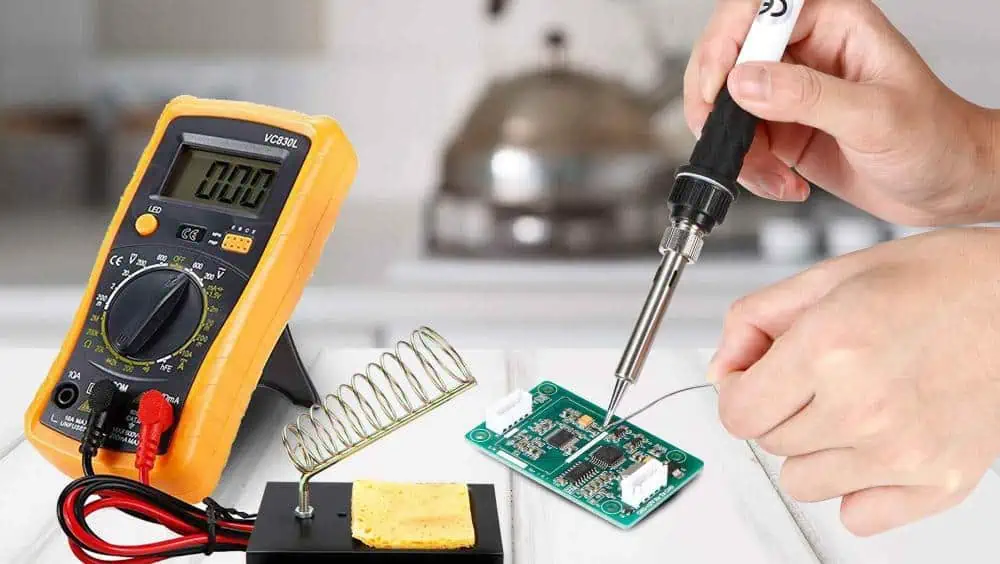
Soldering chip components like resistors, capacitors, and integrated circuits represents an essential skill for assembling printed circuit boards. While seemingly simple, properly soldering chips requires care and proper technique to avoid damaging delicate components or creating unreliable solder joints.
This guide covers everything needed to successfully hand solder chip components of any size onto PCBs. We’ll explore soldering small SMDs under a microscope, soldering leads on through-hole parts, avoiding common mistakes, and inspection steps to ensure quality soldering. With the right tools and methods, assembling chip components can become an easy, rewarding process.
Soldering Tools
Having quality tools makes soldering chip components significantly easier and ensures reliable results.
Soldering Iron
The soldering iron forms the heart of any soldering setup. For chip work, look for:
Fine conical or chisel tip sizes from 0.5mm to 1.5mm
Temperature control for adjusting heat
Power rating from 15W to 65W
Lightweight and ergonomic handle
Temperature control allows matching heat to the size and thermal mass of components. Too little heat risks cold joints while too much damages parts.
Solder Wire
For most electronics work, lead-containing rosin core solder is preferred:
Alloys of 60/40 or 63/37 tin/lead preferred
Diameter from 0.5 to 1.0mm
Rosin core lightly fluxes while soldering
Lead-free solders require higher heat which can damage components.
Hand Tools
Useful hand tools include:
Fine tip tweezers to position and remove parts
Flush diagonal cutters for trimming leads
Vacuum pickup tool for handling tiny SMDs
Optical inspection tools like microscope, magnifier, etc.
Quality hand tools improve precision and avoid damaging PCBs or components.
Soldering Stand and Base
A soldering station helps keep the workspace organized and equipment ready:
Holder safely stores iron when not in use
Stand positions board at convenient angle
Brass wool for tip cleaning
Parabolic tip cleaner
Non-slip rubber base
Spending a bit more for a quality soldering station improves the experience tremendously.
Soldering Technique
With the right equipment, applying proper technique ensures reliable soldering results:
Prepare Components
Any parts like leads or termination pads should be clean and oxide-free for good solder wetting. Use flux or isopropyl alcohol to remove debris. Pre-tinning leads can improve adherence.
Prepare Soldering Iron
The iron tip should be clean, tinned, and set to the appropriate temperature for the part being soldered. Standard tip temperatures range from 650°F to 700°F for most chip work. The iron should reach temperature fully before use.
Heat the Joint, Not the Iron
Place the iron tip simultaneously on the part lead and PCB pad. Give it a few seconds to heat both up before introducing solder. This prevents cold solder joints from insufficient preheat.
Apply Solder
Touch solder against the joint opposite the iron once it is heated. The solder should melt and flow smoothly onto the joint. Use just enough solder to fully coat the joint without excessive buildup. Remove iron and allow the joint to cool undisturbed.
Inspect Joints
Visually inspect each solder joint under magnification after cooling. Look for complete wetting and smooth appearance. Resolder any joints with holes, pits, incomplete coverage, or other defects.
Clean Flux Residue
Remove any residual flux left from soldering using isopropyl alcohol, swabs, and a brush. This prevents corrosion or electrical leakage over time.
Proper technique comes with practice – creating quality solder joints should become second nature after some experience.
Soldering Through-Hole Components
Through-hole (THD) chip components like resistors and capacitors have long axial leads passing through PCB holes. The leads provide mechanical anchoring and allow conduction from both sides of boards. Here is how to approach soldering common THD parts:
Bend Leads
Bend the component leads slightly outward at a 10-20° angle so the body rests flush against the board surface while soldering.
Insert and Align
Insert the leads through corresponding PCB holes. Ensure the part is fully seated against the board surface and properly oriented.
Apply Solder
Heat the joint by touching the iron tip to the lead and pad simultaneously. Apply solder to form a fillet shape until fully covering the joint. Repeat for remaining terminations.
Trim Excess Length
Inspect the joint thoroughly then use flush cutters to trim any excess lead length extending beyond the bottom of the PCB.
With practice, through-hole chips can be quickly installed and soldered for reliable mechanical and electrical termination.
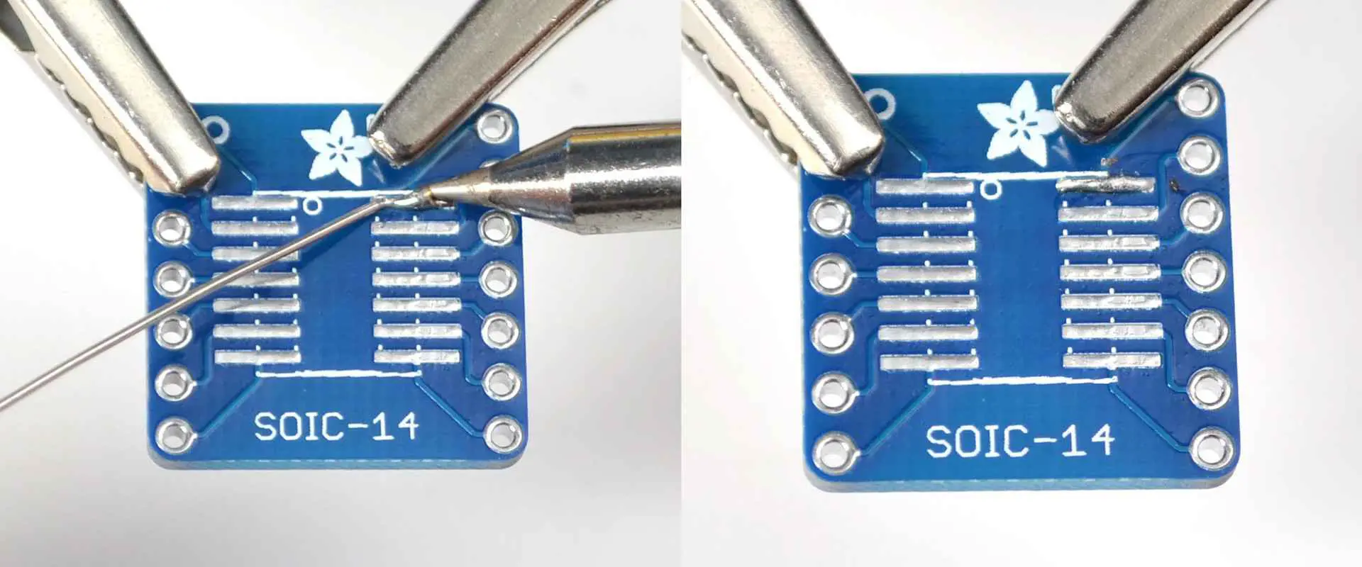
Soldering SMD Components
Soldering tiny surface mount device (SMD) components requires additional care compared to through-hole parts. Follow these guidelines for success with SMDs:
Position Component
Use tweezers or a vacuum pickup tool to precisely place the SMD in the centered in the appropriate PCB footprint. Ensure correct orientation.
Secure Component
To prevent movement while soldering, tack down one pad with minimal solder to hold the component in place. Reheat and adjust position if needed.
Limit Solder Application
Carefully heat each pad and apply a small amount of solder for SMD joints. The solder should wet to the termination and PCB pad without bridging.
Inspect Under Magnification
Thoroughly inspect each individual joint under magnification after soldering. Reflow any joints with insufficient wetting, coverage, or blobs of excess solder.
Taking extra care pays dividends for producing reliable soldering results with tiny SMDs.
Avoiding Common Errors
With attention and care, chip soldering errors can be minimized. Watch out for these potential mistakes:
Insufficient Heat – Not preheating pads enough before applying solder can lead to weak cold joints with poor adhesion.
Excess Solder – Too much solder will blob, bridge, or wick up component leads causing shorts. Use the minimum needed.
Solder Bridges – Solder flowing between adjacent pads creates shorts. Use less solder and inspections can catch any bridge defects.
Overheating – Applying heat too long damages components or PCB pads. Quickly in and out prevents lifting pads.
Cold/Disturbed Joints – Allow every joint to cool undisturbed to prevent cracks, voids, or disturbances weakening the termination.
Flux Residue – Remaining flux left after soldering can lead to corrosion or electrical leakage in the long term if not cleaned.
Catching errors early and reflowing any faulty solder joints prevents headaches down the road after assembly is complete.
Integrated Circuit Packages
Proper soldering technique varies slightly depending on the exact IC package being used:
DIP ICs
Ensure pins are aligned properly before soldering
Heat individual pins quickly without overheating
Inspect for solder bridges between pins
Use desoldering wick if corrections are needed
SOIC / SOP Packages
Minimize solder amount to avoid bridging leads
Inspect thoroughly for hidden solder bridges
Be quick when soldering to avoid heat damage
QFP / TQFP Packages
Tack corner pins first to properly align package
Double check all pins are making contact before soldering
Inspect closely for hidden solder bridges under package
With practice, even challenging components like BGAs can be hand soldered successfully.
Rework and Repair
Despite best efforts, repairing mistakes or reworking soldered chips may become necessary:
Adding More Solder
Apply the iron tip directly to the faulty joint and introduce a small amount of additional solder. This reflows the joint and allows fixing issues like incomplete wetting.
Removing Excess Solder
Use a solder sucker or desoldering braid to remove any excess solder from bridged joints. Carefully reheat the joint and suck up excess material.
Removing Components
For defective or misaligned parts, fully desolder all pins then gently ease the component out while heating the joints. Ensure pads are clean before attempting to reuse.
Repositioning Parts
Likewise, resoldering the joints allows straightening a misaligned part. Take care to avoid lifting pads when reheating and repositioning components.
Developing component rework skill reduces waste and saves projects when minor errors occur.
Thoroughly verifying quality soldering ensures the circuit works reliability into the future.
Conclusion
Soldering chip components requires finesse, patience, and quality tools. With care taken preparing parts and boards, proper soldering technique, and inspecting work, assembling chip components can become an easy and rewarding process. The skills take practice to master, but enable assembling high reliability PCBs.
Frequently Asked Questions
Q: What is the ideal tip size for soldering various chip components?
A: 0.5 to 1 mm conical tips work well for soldering most SMDs and precision work. 1 to 1.5 mm chisel tips allow quick heat transfer for larger pads, DIPs, and THDs.
Q: Is flux required when soldering components with rosin core solder?
A: The flux inside the solder wire core negates need for additional flux in most standard assembly. Added flux can assist with rework or soldering metals like nickel.
Q: What is the proper soldering iron temperature for ICs and semiconductors?
A: 350°F to 400°F offers a good range for soldering temperature sensitive semiconductors without risk of heat damage. Increase temperature for larger joints.
Q: Can soldering chip components reliably be automated?
A: Yes, pick-and-place machines and precision solder reflow ovens automate placing and soldering chips for mass assembly. But careful setup is required.
Q: What magnification is recommended for inspecting solder joints on chip components?
A: A stereo microscope or high quality magnifier in the 10x magnification range allows properly verifying solder fillets, wetting, and bridges on fine chip joints.
How to solder the chip components ?
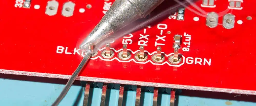
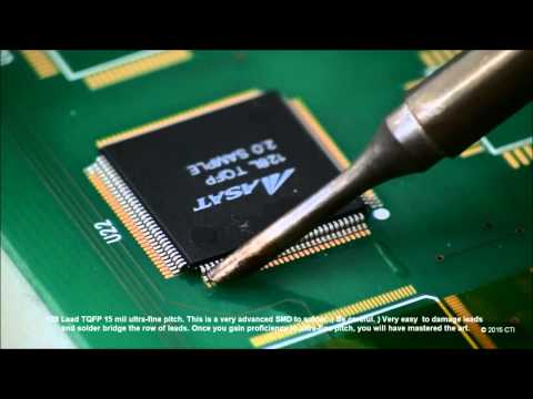
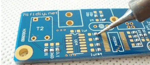
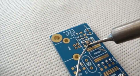
There are two types of soldering methods for chip electronic components:One is manual soldering by soldering the pad with an electric soldering iron, then clamping the end of the chip component with a tweezers, and fixing the other end of the component to the corresponding pad of the device with a soldering iron. After the solder is cooled, remove the tweezers. Then solder the other end of the component with a soldering iron.The second type is machine welding by making a stencil screen, printing the solder paste on the circuit board, and then placing the soldered chip components by hand or machine mounting.
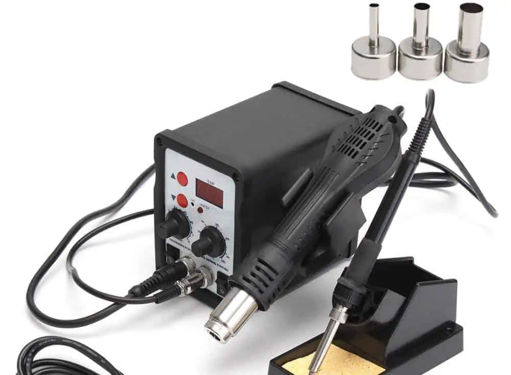
The high temperature soldering furnace solders the chip components.Circuit board, circuit board, PCB board, pcb soldering technology In recent years, the development process of the electronic industry process, we can notice that a very obvious trend is reflow soldering technology. In principle, conventional inserts can also be reflow soldered, which is commonly referred to as through-hole reflow soldering. The advantage is that it is possible to complete all solder joints at the same time, minimizing production costs. However, temperature sensitive components limit the application of reflow soldering, whether it is a plug-in or SMD. Then people turn their attention to selective soldering. In most applications, PCB selective soldering can be used after reflow soldering. This will be the economical and efficient way to complete the soldering of the remaining inserts and is fully compatible with future lead-free soldering,What equipment is needed for board soldering? Solder patch components require a tin spray gun, clip, magnifier, solder paste, rosin oil or paste, etc.SMD component welding diagram
This is an essential tool for soldering patches
This is an essential tool for soldering patches
First solder the solder joint with a soldering
Then clip a patch and go right away.
After the patch is fixed, solder the other side!
Solder IC, first fix one foot of the chip IC on PCB
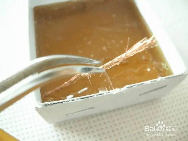
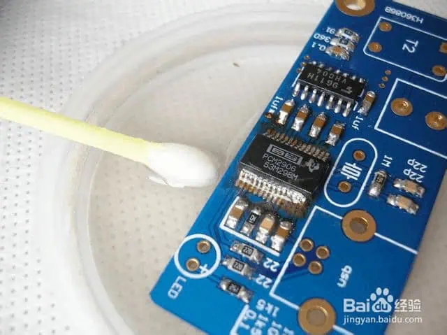
Finally cleaned with alcohol (with a cotton swab)
You will find that the rosin will melt and disappear without seeing it!
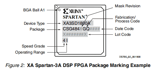
The Xilinx XA Spartan-3A Automotive (XA) FPGA family brings low-cost, reliability-optimized programmable logic to automotive applications. Within this family, the XA3SD1800A-4CSG484Q provides a balance of logic density, features, and package size suitable for body electronics, instrumentation, and engine management systems.
In this article, we will explore the key capabilities and specifications of the XA3SD1800A from its datasheet and reference manual. We’ll examine the programmable logic, hard IP blocks, I/O, reliability, and other relevant details for automotive usage.
These represent a mature toolchain for developing on XA3SD1800A devices.
Conclusion
With its blend of programmable logic, hard IP blocks, automotive-grade qualification, and medium density, the Xilinx XA3SD1800A-4CSG484Q FPGA provides a proven option for cost-optimized automotive applications. The integrated PCIe, Ethernet, memory, and DSP make it well suited for body electronics, gateways, instrumentation, and control systems in next-generation vehicles.
Frequently Asked Questions
Q: How does the XA3SD1800A compare to newer Xilinx Automotive FPGA families?
A: Newer families like XA7 and XA3S provide higher logic density, performance, and features by leveraging smaller process nodes. But XA3SD offers a cost-optimized legacy option.
Q: What is the typical static power consumption for the XA3SD1800A FPGA?
A: Static power depends on configuration but is typically 130-200mW. Active power peaks around 1.5W for complex designs.
Q: What is the maximum supported transceiver speed in the XA3SD1800A?
A: The integrated PCIe block supports Gen 1 speeds up to 2.5Gbps. GTX transceivers can reach up to 3.75Gbps using external SERDES.
Q: Does the XA3SD1800A support functional safety features?
A: While not ASIL-certified, the XA3SD family does provide SEU mitigation and other features to help meet ISO26262 requirements.
Q: What configuration bitstream storage is recommended for the XA3SD1800A?
A: An 8Mb SPI flash provides room for multiple bitstreams. Larger memories provide storage for more FPGA images.
XA devices are available in both extended-temperature Q-Grade (–40°C to +125°C TJ) and I-Grade (–40°C to +100°C TJ) and are qualified to the industry recognized AEC-Q100 standard.
The XA Spartan-3A DSP family builds on the success of the earlier XA Spartan-3E and XA Spartan-3 FPGA families by adding hardened DSP MACs with pre-adders, significantly increasing the throughput and performance of this low-cost family. These XA Spartan-3A DSP family enhancements, combined with proven 90 nm process technology, deliver more functionality and bandwidth per dollar than ever before, setting the new standard in the programmable logic industry.
Because of their exceptionally low cost, XA Spartan-3A DSP FPGAs are ideally suited to a wide range of automotive electronics applications, including infotainment, driver information, and driver assistance modules.
The XA Spartan-3A DSP family is a superior alternative to mask programmed ASICs. FPGA components avoid the high initial mask set costs and lengthy development cycles, while also permitting design upgrades in the field with no hardware replacement necessary because of its inherent programmability, an impossibility with conventional ASICs and ASSPs with their inflexible architecture.
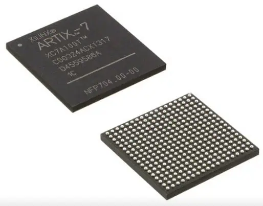
The Xilinx XA Spartan-7Automotive (XA) FPGA family brings low-power programmable logic to next-generation vehicle systems. Within this family, the XA7A75T-1CSG324Q provides a balanced mix of density, features, and I/O for ADAS, infotainment, connectivity, and other automotive applications.
In this article, we will take a technical deep dive into the XA7A75T FPGA to understand its capabilities, architecture, available resources, and benefits for automotive use cases. We’ll explore the data sheet specifications and configuration options that enable successful deployment of this FPGA.
The Xilinx XA7A75T sits in the middle of the XA Spartan-7 lineup with these high-level characteristics:
75K logic cells
5.3Mb block RAM
240 DSP slices
PCIe x1, Gigabit Ethernet blocks
324 user I/O pins
7.5 x 7.5 mm, 0.8mm pitch FC-BG484 package
Wide variety of automotive I/O standards
Power optimized at 0.85W typical consumption
These resources provide ample density for feature-rich automotive systems, balanced with restraints on cost and power consumption. The integrated PCIe, Ethernet, memory, and DSP blocks accelerate key functions while minimizing FPGA resource usage.
FPGA Logic Cells
The core FPGA fabric that implements custom logic consists of 75,000 logic cells, organized into a matrix of configurable logic blocks (CLBs).
Each CLB contains 8 LUTs and 16 flip-flops
256-bit shift registers for memory and delay elements
Built on TSMC’s 16nm FinFET process, the FPGA fabric offers high density and performance per watt. Accelerator blocks like DSP slices connect seamlessly into the interconnect fabric.
Block RAM
For data buffering and storage, the XA7A75T provides 5325 Kb of fast block RAM, organized into 330 dual-port 36 Kb blocks.
Key capabilities:
Dual or single port configurations
Optional ECC detection and correction
Configurable width and depth
6000 memory accesses per second
Cascading for wider memory width
The abundance of block RAM enables on-chip data manipulation without external memories.
DSP Slices
For arithmetic processing, the FPGA includes 240 DSP slices, each providing:
25 x 18 bit signed multiply with 48-bit accumulate
Cascade to 96 bits for high precision
Optional pipelining and shifting
Overflow and saturation protection
Fast DSP carry chain
The many DSP slices enable parallel signal processing tasks for vision, radar, lidar, and machine learning applications.
PCIe Block
The integrated PCIe block provides a x1 Gen2 lane connection, with:
PCIe 2.1 compliant interface
2.5 Gbps line rate
Auto negotiation speed selection
AC-coupled differential RX
Multiply options for refclk input
MGT and logic interface
This enables high bandwidth local interconnect to processors and other peripherals without consuming FPGA fabric resources.
Ethernet Blocks
Two tri-speed ethernet MAC blocks support 10Mbps, 100Mbps, and 1Gbps operation with:
1500 byte jumbo frame support
RGMII interface to external PHY
Scatter-gather DMA networking
Low latency cut-through operation
Unicast and multicast addressing
Combined with an external PHY, the MAC blocks enable robust automotive ethernet connectivity.
FPGA Clocking
The clocking subsystem allows very flexible control over clock sources, routing, and conditioning:
Up to 7 clock management tiles (CMTs)
Mix of PLLs, DLLs, and DCMs
Frequency synthesis, jitter filtering, and deskew
Multiple clock input options with muxing
Global low-skew routing
This provides ultra precise clocks derived from commodity oscillators to sequence critical automotive logic.
XA7A75T Packaging
The XA7A75T FPGA is packaged in a FCBGA484 package optimized for automotive reliability:
These ensure suitability for safety-critical automotive applications and deliver high long-term reliability.
Development Tools
Xilinx provides a full embedded development toolchain:
Vivado Design Suite for building hardware
Vitis tools for creating software
PetaLinux for Linux OS support
Model based design with System Generator
Extensive IP catalog of automotive peripherals
Reference designs and use cases
These enable rapid development of capable automotive systems leveraging the XA7A75T FPGA.
Conclusion
With its balanced density, ample hardened blocks, power efficiency, and automotive-grade qualification, the Xilinx XA7A75T FPGA provides an optimized platform for advanced driver assistance systems, vehicle connectivity, infotainment, and instrumentation applications. The integrated PCIe, ethernet, memory, and DSP enable necessity in-vehicle functions while minimizing logic resource usage. For automotive engineers looking to add flexible programmable logic, the XA7A75T delivers proven reliability, connectivity, and real-time processing.
Frequently Asked Questions
Q: What are the main advantages of the XA7A75T compared to microcontroller-based designs?
A: The FPGA fabric enables custom parallelism, hardware acceleration, and real-time responsiveness that goes beyond sequential microcontroller execution.
Q: What is the power consumption difference between the XA7A75T vs non-Automotive grade FPGAs?
A: The XA family focuses on minimizing power, with 40% lower static power and up to 30% lower total power versus equivalent non-Automotive devices.
Q: What is the maximum operating speed of the FPGA fabric in the XA7A75T?
A: The typical fMAX is 450MHz. Actual speed depends on the design complexity and routing, with potential to reach over 500MHz in optimized cases.
Q: Does the XA7A75T support functional safety features?
A: Xilinx offers a Safety Package for these FPGAs that provides SEU immunity, fault injection, and other features necessary for ISO 26262 ASIL-B/C compliance.
Q: What is the typical configuration flash storage for the XA7A75T bitstream?
A: A 16MB SPI flash provides ample room for multiple bitstream configurations with redundancy. Smaller serial flashes can work depending on design size.
1. A user configurable analog interface (XADC), incorporating dual 12-bit 1MSPS analog-to-digital converters with on-chip thermal and supply sensors.
2. Single-ended and differential I/O standards with speeds of up to 1.25 Gb/s.
3. 240 DSP48E1 slices with up to 264 GMACs of signal processing.
4. Powerful clock management tiles (CMT), combining phase-locked loop (PLL) and mixed-mode clock manager (MMCM) blocks for high precision and low jitter.
5. Integrated block for PCI Express® (PCIe®), for up to x4 Gen2 Endpoint.
6. Wide variety of configuration options, including support for commodity memories, 256-bit AES encryption with HMAC/SHA-256 authentication, and built-in SEU detection and correction.
7. Low-cost wire-bond packaging, offering easy migration between family members in the same package, all packages available Pb-free.
8. Designed for high performance and lowest power with 28 nm, HKMG, HPL process, 1.0V core voltage process technology.
9. Strong automotive-specific third-party ecosystem with IP, development boards, and design services.
10. Some key features of the CLB architecture include:
Register and shift register functionality The LUTs in 7 series FPGAs can be configured as either one 6-input LUT (64-bit ROMs) with one output, or as two 5-input LUTs (32-bit ROMs) with separate outputs but common addresses or logic inputs. Each LUT output can optionally be registered in a flip-flop. Four such LUTs and their eight flip-flops as well as multiplexers and arithmetic carry logic form a slice, and two slices form a configurable logic block (CLB). Four of the eight flip-flops per slice (one per LUT) can optionally be configured as latches. Between 25–50% of all slices can also use their LUTs as distributed 64-bit RAM or as 32-bit shift registers (SRL32) or as two SRL16s. Modern synthesis tools take advantage of these highly efficient logic, arithmetic, and memory features.