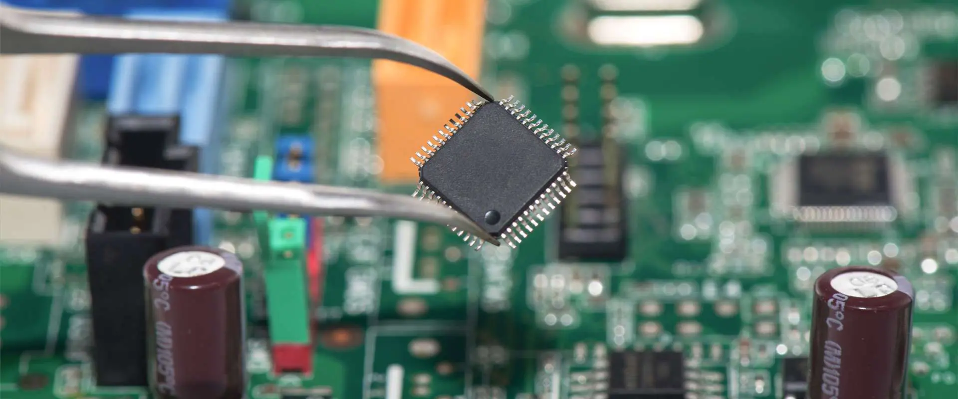
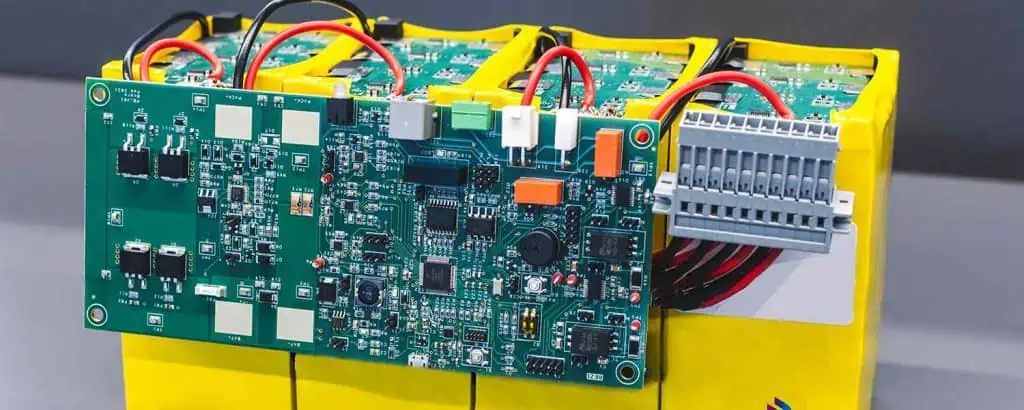
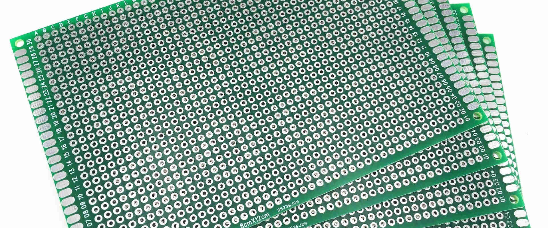
When we talk about hardware of printed circuit boards, the mounting type and material are very important. We advise that before going ahead to make your purchase, you request for free samples. This will convince your team that they have the best solution.
This ultimate guide is there to give an introduction to the buyers. To get professional advice, we are here and happy to help you. Please continue reading to learn about the hardware pcb you need

Components of PCB Mounting Hardware
Here are the components of printed circuit boards which will be needed by your team.
Supports
These are also referred to as support posts or support pillars of the PCB. These are great for white goods. When you use your application constantly, then you’ll need reliable components. From their name, they give support to the mounting of the PCB. This they achieve by joining the board of your PCB to the surface.
Apart from this, they add some protection and insulation from electrical transmission, coupled with offering a hold that is more stable and secure. Regarding materials, you have two options to choose from – metal and plastics. With plastics, your PCB will become lighter, and you may prefer the easy installation process that these supports provide.
Mounting options may be different, and include screw locking, reverse locking, snap lock, and adhesive edge locking.
- Snap-Lock: This pushes into a chassis or panel hole. This gives a secure fix that can be easily released.
- Blind hole/press fit: These fins hold some binding holes securely with a unique painted style, which drives with ease into applications.
- Snap-Fit: This pushes quickly into a chassis hole or panel, ensuring that the mounting is efficient and strong. This saves your time when the installation process is on.
- Adhesive base: The adhesive tape gets rid of the use of mounting holes. This provides space and time efficiencies.
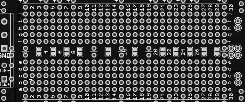
PCB spacers and standoffs
The PCB spacers and standoffs do well in positioning the components and maintaining space within your PCB. The shapes of both can be the same. You’ll either have a hexagonal spacer or a hexagonal standoff. Also, you can choose round spacers or a round standoff.
But what’s the difference? For spacers, they are not threaded. Standoffs on the other hand, are threaded on the two ends and are available in both female and male designs. At times, you’ll see a description like “threaded round spacer”. Clearly, it is a standoff due to its threaded nature. The fact is that both of them serve the same purpose, with the only difference being if they are threaded or not.
Materials: ceramic, metal, or plastic?
The materials vary. In cases of applications that use very high temperatures, make use of ceramic spacers. Printed circuit board plastic spacers like Nylon PCB standoff are cost-effective to ensure mass production, and provide a strong resistance against corrosion. Even with this, they boast great mechanical properties. Also, if you need a lightweight option, they are preferable compared to metal.
Card guides
Card guides are another circuit board mounting hardware, which are useful whenever you are in tight spaces. A good example here is the PCB rack. Make use of a horizontal PCB card guide or a vertical one depending on the PCBs mounting direction in your application.
These card guides are usually used in saving space and preventing the bending of the boards. Installing them is easy as well and some feature adhesive backs, while some others provide you with a locking action. The two will offer more stability to your PCB. Furthermore, some alternatives assist whenever your PCB needs to be protected from vibration and shock.
Card Pullers and Ejectors
Card ejectors, which are also referred to as extractors, inserters, and pullers, are usually attached to help in relieving stress, which is brought to the PCB, as well as its circuitry. It achieves this by removing the card from spaces that are restricted.
The mounting is done on the board itself, offering a handle to enable the board to be pulled out easily by the technician, without getting to the circuitry. What we mean is that, this card ejector serves as a lever. It makes use of mechanical force against a chassis or guide rack.
The puller of the circuit board fits to a PCB in order to help it pull out, as well as push back into its position. This is used whenever you are faced with a difficult insertion, as well as extraction issues. This means you will have to deal with the stress involved in the removal of large Printed circuit boards and multi-pin tight-gripping edge connectors.
Mounting Blocks for PCB

These mounting blocks are utilized in interconnecting connectors that are solderless to a PCB. This mounting block offers both mechanical and electrical connection between the board and the chassis. They are very useful when mounting small panels and printed circuit boards at ninety degrees within your application.
The PCB mounting blocks are well known in different industries, this includes consumer electronics, telecommunications, and automotive.
Fuse Covers
Fuse covers help in encasing electrical fuses, thereby offering protection and insulation. This cover provides insulation, gives cover for electrical fuses, and protects from liquids and contamination.
PCB Fan Accessories
For the heat management of your PCB, your best choice should be fans. To enhance the efficiency and safety of your fan, you must possess the right parts.
Fan guards
These prevent water and dust ingress, thereby offering some protection for your PCB. Regarding fan parts as well as fan guards, materials vary. There are plastic and metal fan guards available, whatever you choose will depend on the strength and look you want and the option that goes in line with your budget. Compared to the metal fan guards, the plastic type is more versatile.
Fan gaskets
Fan gaskets help in delivering the vibration and noise insulation needed when preventing the leakage of air. When the small gap is sealed between the housing and the fan, there is great improvement in efficiency, minimized feedback airflow, and with this, air pressure losses.
Fan rivets
While mounting the fan, this process can be simplified and money and time saved by replacing nuts and screws, with fan rivets. These rivets come with prongs, which expands in order to hold properly while the pin is being driven in. There’s another option, which is the push fan rivet. They can be installed with ease as well and expanded when it is pushed in to fit tightly. To detach it, all you need to do is to remove the head.
Fan mounts
Fan mounts help in securing and positioning your fan. These rubber anti-vibration fan mounts help in reducing any noise that the fan can produce. Usually, these fan mounts are manufactured from elastomers like ABS or silicone rubber.
Fan filters
Fan filters help in removing small particles or dust from the airflow of fans to prevent any damage from happening internally. You can choose a fan filter made of metal. Examples here include aluminum and stainless steel. These filters will permit the free flow of air. Cleaning them is also very easy, and they have a sleek design. You can also choose felt fan filters. They are usually difficult to clean, but it performs a great job of keeping dust away. In addition, the design of felt fans consumes more space.
To get the best convenience, get a fan filter set. This offers you a filter cover, felt filter, mesh filter, and finger guard.
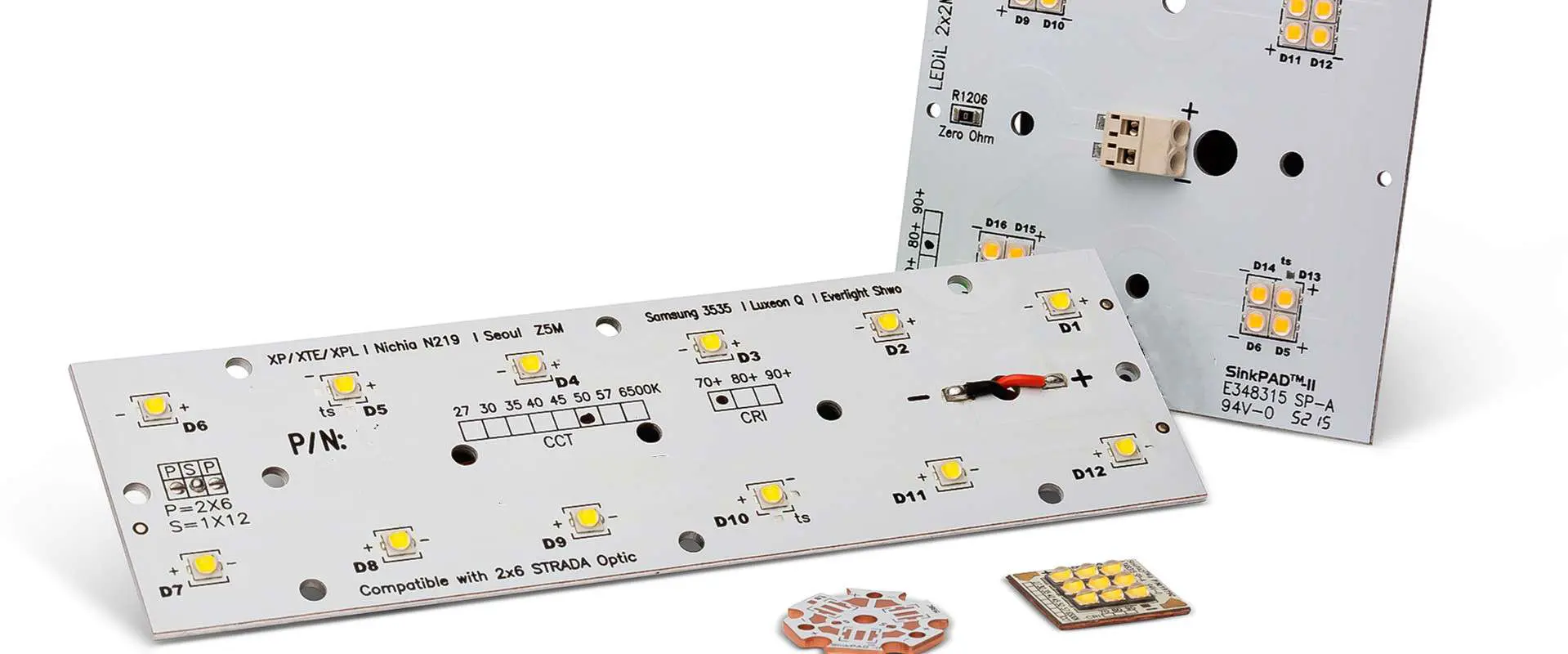
LED Mounting Hardware
Components of LED like LED spacer mounts restrict movement and position your LED lights. These spacers offer more height conformity, rigidity, and stability. This stability and rigidity ensures that the manufacturing process comes easier. Also, it is important when servicing the board, or whenever there is a need to repair the PCB, as well as other parts.
Some other critical components are the LED holders and mounts. The LED light mount usually features holes that pass the leads. After this the LED is then soldered to the PCB. Since, there may be differences in through hole LED sizes, the LED spacer you are using must possess the correct number of holes. This will help in taking the leads attached.
When handling applications where the mounting of the LED is not done on the PCB directly, then you must use a LED lens holder. You may also require an LED light pipe. This helps in the transmission of light from the PCBs LED mounting. The light pipe technology of LED translates to great visual performance, delivering uniform lighting. Also, it reduces glare and shadows significantly. They also come with another great advantage, which is their ease while installing them.
Conclusion
By now, you should have gained vast knowledge about PCB hardware. For PCB hardware, the mounting type and material are very important. Always request for free samples, before making any purchase. This will convince your team that they have the best solution. To get professional advice, we are always here and happy to help you.