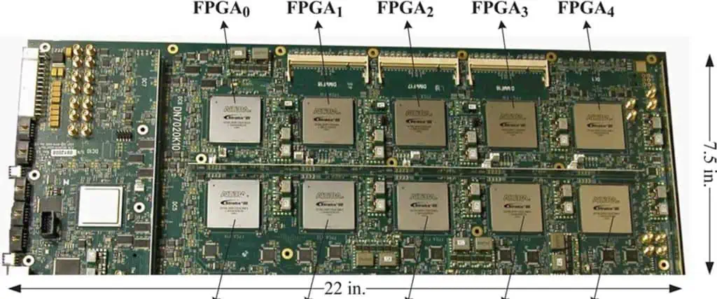
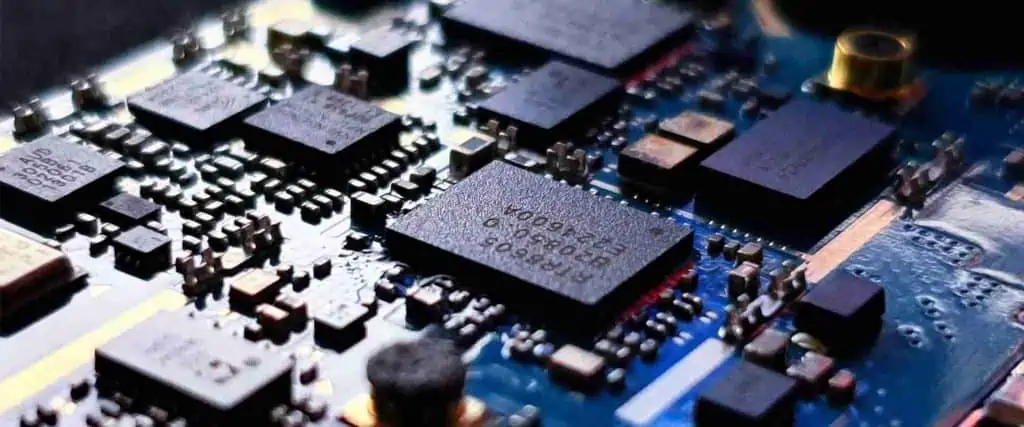
The Xilinx XC7Z020-2CLG400i device belongs to the Zynq-7000 family and is grounded on the SoC architecture of Xilinx. The device is integrating a dual or single-core ARM Cortex processor that has rich features. The processor is grounded on the processing system and is having 28nm of programming logic. The central processing unit of the device is considered the heart of the processing system and is comprising of on-chip memory, state-of-the-art interfaces for peripheral connectivity, and interfaces for external memory too. The central processing unit has 2.5 DMIPS per MHz through each CPU with a frequency capability of 1 GHz. The device has coherent multiprocessor support, a couple of triple-timer counters, a global timer, 3 watchdog timers, and interrupts.
The device has caches of up to 32Kb of level-1 that have 4-way set-associative instructions and is independent of each CPU. There is also a 512Kb of level-2 that has 8-way set-associative instructions and is shared in between central processing units. Furthermore, the caches are having byte-parity support as well. Xilinx XC7Z020-2CLG400i has 256Kb On-Chip RAM and ROM with byte-parity support. This IC has a multi-protocol controller for dynamic memory with 32 or 16-bit interfaces for LPDDR2, DDR2, DDR3L, and DDR3 memories. The device has 16-bit support for ECC. It has an SRAM data bus of 8 bits with 64Mb support, parallels support for NOR flash, and 8 channel DMA controller capable of support for scatter-gather transactions, peripheral to memory, memory to peripheral, and memory to memory. The interconnects of the device are having a high-bandwidth connection for its PS and among PL and PS. The configurable logic block of Xilinx XC7Z020-2CLG400ihas cascaded adders, flip-flops, and lookup tables. Block RAM is dual-port, expandable up to 72 bits, and can be configured in the form of dual 18Kb block RAM too. The DSP block has a pre-adder of 25-bit, accumulator or adder of 48-bit, and a signed multiplier of 18×25 bits. Its PCI block is supporting up to 8 lanes, 2nd generation speeds, along with endpoint configurations, and root complex.
The family of Xilinx XC7Z020-2CLG400i is Zynq-7000 which offers scalability and flexibility of FPGAs delivering ease of use, power, and performance usually associated with ASSPs and ASICs. The devices of this family are allowing the designers to target cost-sensitive and higher performance enabled applications through a single platform through the use of tools of industry-standard. All of the devices of the family are having identical PS but PL and input/output resources are varying in all devices. The device is utilized for a wide range of applications as in the automotive industry it has applications in driver assistance, information for drivers, and infotainment. It is used in broadcast cameras, machine vision, industrial networking, and motor control. Smart and IP cameras have also been used along with baseband and LTE radios. The device is used in biomedical imaging, diagnostics, multi-function printers, night-vision equipment, and video devices.
Memory Interfaces
The unit of memory interfaces of the Xilinx XC7Z020-2CLG400i device is comprising of controllers for dynamic and static memory interfaces. The interface for dynamic memory is supporting DDR3L, LPDDR2, DDR3, and DDR2 memories. While the interface of static memory is having support for interfaces of NOR flash, quad-SPI flash, parallel data bus, and static flash interface.
Interfaces for Dynamic Memory
The DDR memory controller which is a multi-protocol controller could be configured for delivering 32 or 16-bit broad accesses to its 1Gb address spaces through the utilization of a unity rank configuration for 8, 16, or 32-bit DRAM memories. The support for ECC is in the form of a 16-bit mode for bus access. The PS of Xilinx XC7Z020-2CLG400i is incorporating both associated PHY and DDR controllers encompassing its integrated inputs/outputs. The device is supporting up to the speed of 1333Mb/s for its DDR3 support. The DDR memory controller is multi-ported and is enabling the system processing and its programmable logic for common access to have a shared memory. There are 4 AXI slave ports in the DDR controller for this purpose. One of the 64-bit ports is having the purpose of ARM CPU through the controller of L2 cache and could be configured for lower latency. Two 64-bit ports are dedicatedly assigned to PL access. One of the 64-bit AXI ports is common for all of the AXI masters through a central interconnect.
Interfaces for Static Memory
The memory interfaces of Xilinx XC7Z020-2CLG400i for static memory are supporting external static memories. The 8-bit SRAM data bus is supporting till 64Mb, while the 8-bit NOR flash parallel data bus supports up to 64Mb. The integrated ONFI NAND flash is supporting up to 1-bit ECC. Whereas, 1, 2, and 4-bit SPI or a couple of quad-SPIs each of 8 bits are supported through serial NOR flash.
The Input / Output Peripherals of Xilinx XC7Z020-2CLG400i
The input/output peripheral unit of the device is consisting of peripherals for data communication. The key features of the unit comprise two tri-mode peripherals for Ethernet MAC having support for IEEE standard 1588 and IEEE standard 802.3. The device also has the capability of scatter-gather DMA. Xilinx XC7Z020-2CLG400i has a feature for recognition of 1588 revision for 2 PTP frames. It also supports an external PHY interface along a couple of USB 2.0 peripherals of OTG mode each having support of 12 endpoints. The device is entirely compliant with USB 2.0 standards with host and device IP core. It delivers an 8-bit external PHY interface for ULPI. It has 2 full CAN buses fully compliant to CAN 2.0B interfaces. With the utilization of its TrustZone system, 2 ethernets, 2 SDIO, and 2 USB ports are configurable in both non-secure and secure modes. The input/output peripherals are also communicating with the external devices via shared pool of 54 integrated multi-use input/output pins. Every peripheral could be assigned to either of its many pre-defined pin groups that enable flexible assignment of numerous devices on a simultaneous basis. Though all of its 54 pins are not capable to be used simultaneously for its input/output peripherals but most of its input/output interfaces for signals are available for PL to enable utilization of standard PL at input/output pins in powered ON conditions.
The Xilinx XC7Z010-2CLG400i belongs to the Zynq-7000 series of devices. This device is available in various speed grades such as -1, -3, -1LI, and -2. The best performance is only with using -3 speed grade IC. The device of -1LI is capable of operating in a couple of programmable logic modes with its VCCBRAM or VCCINT to be 1.0V and 0.95V and are also separated for lower minimal static power. The specification of speed for -1 speed grade is identical to that of -1LI type speed grade. The dynamic and static power of the -1LI speed grade is reduced with it is operated in the VCCBRAM or VCCINT to be 0.95V.
The AC and DC characteristics of Xilinx XC7Z010-2CLG400i are categorized in different types such as expanded, commercial, industrial, extended, and defense temperature ranges. The only exception lies within the operational temperature range elsewhere, entire AC and DC electrical and electronic parameters are identical for all speed grade devices. Taking an example of the -1-speed grade device for industrial application has its timing characteristics identical to that of -1 speed grade devices used for commercial applications. Though, a specific range of devices are there for Q-temp, extended, industrial, and commercial ranges of temperature. The entire range of specifications for junction temperature and supply voltage is the representation of a worst-case scenario for the device. All of the included parameters are commonly considered for typical applications and popular designs.
For the device Xilinx XC7Z010-2CLG400ithere is a specific powering ON sequence recommended by manufacturers starting with VCCPINT followed by VCCPAUX and VCCPLL and PS VCCO supplying power to VCCO_MIO0, VCCO_DDR, and VCCO_MIO1 for achieving minimal drawl of current and ensuring all of input/outputs to be the three-stated power ON stage. Whereas, the input of PS_POR_B is necessary for GND assertion during the power ON stage till VCCO_MIO0, VCCPAUX, and VCCPINT reach a minimal level of operation for ensuring the integrity of PS eFUSE. The preset setting of the device can be referred to when considering additional information regarding PS_POR_B timing.
The power OFF sequence for the Xilinx XC7Z010-2CLG400i as per the recommendation of its manufacturers is opposite to that of the power ON sequence. At a time when PS VCCO, VCCPLL, and VCCPAUX supplies are having an identical level of voltages, then all of these can get power through the same supply and can be ramped together as well. Xilinx is recommending delivering power to VCCPLL and VCCPAUX with one supply along with a ferrite bead filter. Beforehand, VCCPINT has reached the voltage of 0.80V, one of the conditions is required to be followed during the power OFF stage of the device. For example, the input of PS_POR_B is to be inserted to GND, the input of PS_CLK clock reference is to be disabled, VCCPAUX must be lower than 0.70V, or VCC_MIO0 is to be set at a value lower than 0.90V. Any of the aforementioned conditions must be set till the time when VCCPINT has reached a value of 0.40V for ensuring the integrity of PS eFUSE.
For the voltages of VCCO_MIO1 and VCCO_MIO0 to be 3.3V, the difference in voltage among VCCPAUX and VCCO_MIO1 or VCCO_MIO0 should not increase more than 2.625V for every Power ON/OFF cycle to maintain the level of reliability of the device Xilinx XC7Z010-2CLG400i.
Xilinx XC7Z010-2CLG400i PL Power Supply Sequence
The recommended PL power ON sequence for Xilinx XC7Z010-2CLG400iby manufacturers is to start with VCCINT followed by VCCBRAM, then VCCAUX, and end at VCCO for achieving minimal drawl of current to ensure the inputs/outputs to be in three-stated power ON state. Xilinx is recommending the power OFF sequence for the IC to be opposite to its power ON sequence. When VCCBRAM and VCCINT are having identical levels of voltages, then both of these could be powered with one supply and ramped together. For the voltages of VCCO to be 3.3V in configuration bank 0 and input/output bank, the difference of voltages among VCCAUX and VCCO should not be exceeding 2.625V for every power ON/OFF cycle for maintaining levels of reliability of the device.
GTP Transceivers
Xilinx XC7Z010-2CLG400ihas a recommended sequence for its powering ON for achieving minimal drawl of current for its transceivers. The sequence starts with VCCINT, followed by VMGTAVCC, VMGTAVCC, or VMGTAVTT, then VCCINT, and ends at VMGTAVTT. VCCINT and VMGTAVCC both could be ramped together. Whereas, the powering OFF sequence recommended by Xilinx for the device is exactly opposite to its power ON sequence for achieving minimal drawl of current.
In case, if the recommended power ON/OFF sequences is not followed, then the drawn current from VMGTAVTT could be more than its requirements during its power ON/OFF cycle. At the time when VMGTAVTT is given power before VMGTAVTT-VMGTAVCC and VMGTAVCC are greater than 150mV and resultant VMGTAVCC is less than 0.7V but VMGTAVTT draws current with an increment of 460mA through every transceiver during the ramp-up of VMGTAVCC. The current drawl duration could be about 0.3 times VTMGAVCC. Whereas, its opposite procedure is true for its powering DOWN. At the time when VMGTAVTT is given power before VMGTAVTT-VCCINT and VCCINT are greater than 150mV and its VCCINT is less than 0.7V then its resultant drawl of current through VMGTAVTT could increment by 50mA through each transceiver while VCCINT is ramping up. The current drawl duration could also go up to 0.3 times VTCCINT. The opposite process is true for its powering DOWN.
There are specific minimal current requirements for Xilinx XC7Z010-2CLG400i when it comes to powering ON of the device and its configuration setting. When minimal current requirements are fulfilled, the device is powered ON and all of its 4 PL power supplies get through their power ON threshold for voltages. The device should not be put in configuration mode till VCCINT is applied to it. Xilinx power estimator tool should be utilized after configuration and initialization for estimation of drain current on the supplies.
DC Output and Input Levels
The VIH and VIL values are recommended by Xilinx for input voltages of Xilinx XC7Z010-2CLG400i. Whereas, the values for IOH and IOL are assured for operating conditions that are recommended at testing points of VOH and VOL. Only specific standards are tested. The specific standards are supposed to be tested at a minimal value of VCCO along with its respective VOH and VOL level of voltages.
Electronic circuits are interconnected networks of electronic components designed to perform a specific function. Circuits are the fundamental building blocks of all electronic devices and systems. They process signals using a combination of active components like transistors, diodes, integrated circuits along with passive components such as resistors, capacitors and inductors powered by a voltage or current source. The combination and configuration of components determines the operation and purpose of the circuit. This article provides an introduction to the key concepts, fundamental analog and digital circuits, common applications and frequently asked questions about this broad field.
Electronic Components for Circuits
Electronic components can be categorized into two main groups – active components and passive components:
Active Components
Transistors – Semiconductor devices used for amplifying and switching signals
Integrated Circuits – Microchips integrating multiple transistors and components
Vacuum Tubes – Early amplifier device preceding transistors
Diodes – Allow current flow in only one direction
Passive Components
Resistors – Limit and resist current flow
Capacitors – Store electrical charge and filter signals
Inductors – Store and release electromagnetic energy
Transformers – Transfer electrical energy between two circuits
Selecting the right components and combining them properly allows implementing innumerable circuit functions.
Circuit Diagrams
Circuit diagrams use standardized symbols to describe the components and interconnections in a circuit. They serve as an engineering blueprint for constructing and analyzing circuits. Standardized schematic symbols represent each component type, with lines between them showing electrical nodes and branches.
Common electronic component symbols
Circuit diagrams provide a quick visual representation of the circuit function and topology. They allow simulating and optimizing the circuit before constructing it physically.
Electronic circuits can be categorized into two major classes – analog circuits and digital circuits:
Analog Circuits
Signals are continuous, typically voltage or current waveforms
Amplitude and frequency vary over time
Used for functions like amplification, filtering, modulation
Designed using principles of analog electronics
Typical analog circuit – an amplifier
Digital Circuits
Signals have discrete on-off or high-low logic levels
Represent numeric values, characters, logic states
Used for data processing, computing, logic, memory
Designed using gates, flip flops, microcontrollers
Example of a digital counter circuit
Both analog and digital circuits are essential building blocks of modern electronics and serve very different purposes.
Power Supplies for Electronic Circuits
All electronic circuits require power supplies to operate. Power supplies convert main AC voltage to the required low level AC or DC voltages to energize a circuit.
AC-AC converters – Convert 120/220VAC mains down to lower AC to run heaters, motors, lights
AC-DC converters – Rectify and filter AC into a DC level like 5V or 12V for most electronic circuits.
DC-DC converters – Switch and convert a DC source to a different voltage level
Linear Regulators – Regulate the DC output voltage against load changes
Switch Mode Regulators – Efficient high frequency DC-DC conversion
Power supplies employ transformers, rectifiers, filters, linear and switching regulators to deliver stable, appropriate voltage and current levels. Well designed power systems are critical for proper functioning of electronic circuits.
Fundamental Analog Circuits
Analog circuits work with signals free to vary continuously in time. They are extensively used for interfacing with sensors, instrumentation, control systems and real world signals. Here are some fundamental analog circuit types:
Voltage Divider
A simple circuit producing an output voltage (Vout) that is a fraction of its input voltage (Vin). Composed of two resistors in series, with the voltage dropped across each resistor proportional to its resistance.
Used for measurement, sensing, monitoring, and voltage reduction.
Current Mirror
Mirrors the current flowing in one active circuit branch into a second branch by matching the V-I characteristics of two transistors. This forces the second branch current to match the reference current in the first branch.
Used extensively in integrated circuits to bias active components.
Voltage Amplifier
Uses transistors to amplify low level input signals to produce larger output signals while maintaining the original signal shape and frequency. The gain determines the amplifier voltage multiplication ratio.
Essential for boosting sensor signals, audio systems, instrumentation.
Active Filters
Use active components like op-amps combined with resistors and capacitors to produce various filter response shapes like low-pass, high-pass, bandpass, notch and all-pass.
Widely used for audio processing, control systems, radio communications and more.
These form the core analog functions integrated into more complex circuits and ICs.
Fundamental Digital Circuits
Digital circuits operate on discrete signal levels representing binary 1s and 0s. They perform calculations, data processing, encoding and logic operations by combining basic building blocks. Common digital circuit blocks include:
Logic Gates
Process one or more binary inputs to produce a single binary output according to a Boolean logic function. Basic gates include AND, OR, NOT, NAND, NOR, XOR, XNOR. Combining gates enables complex logic functions.
Used throughout computer systems and embedded devices for data processing and control logic.
Flip-Flops
Bistable multivibrator circuits with two stable output states based on clock timing and input gates. Latch the current data input or maintain the previous value based on the clock. Types include D, JK, T.
Essential components for registers, counters, finite state machines and digital systems.
Multiplexers
Use a control input to switch a common output between multiple input sources. The selected input connection is passed through to the output via high speed electronic switches.
Used extensively to reduce circuit interconnect complexity in large scale ICs and systems.
Analog to Digital Converters (ADCs)
Convert continuous analog signals like audio, video or sensor data into discrete digital values for processing. Common types include successive approximation, integrating, flash, and sigma-delta ADCs.
Essential for digital capture, analysis and storage of real-world analog signals.
Digital circuits underpin the incredible advances in modern computing, embedded systems and communications.
Printed Circuit Boards
Printed circuit boards (PCBs) provide the physical base for assembling electronic circuits and components. PCBs have conductive copper traces etched on an insulating substrate that interconnects the components mechanically and electrically. They provide the pathways for signals and power.
Assembled PCB with components
PCBs allow constructing multilayer circuits with much higher component densities versus point-to-point wiring. They are essential for all but the simplest electronic devices.
Electronic circuits power functionality across every sphere of technology, industry, science, and daily life. Nearly all electronic devices and systems are enabled by integrated circuits and PCBs populated with discrete components.
Some major applications include:
Computing – Microprocessors, memory, data storage, interfaces in PCs, servers, embedded systems
Communications – Radio, cellular, WiFi, Bluetooth modules for transmitting/receiving data
Industrial – PLCs, instrumentation, process control systems, robotics
Medical – Patient monitors, imaging equipment, diagnostics, prosthetics
Electronics and circuits are integral to all modern technological capabilities we depend on across every industry and domain.
Circuit Design Process
Designing electronic circuits involves an iterative workflow and optimization:
1. Define Requirements
Define the application, inputs, outputs, modes, and performance specifications expected from the circuit.
2. Concept Generation
Research existing solutions, circuits, and ICs applicable to the requirements. Identify viable circuit architectures and blocks to provide desired functionality.
3. Circuit Simulation
Use SPICE or other analog/digital simulation tools to model the proposed circuit virtually. Simulate and validate expected behavior meets specs.
4. Schematic Capture
Draw up detailed circuit schematics with components, interconnects, and construction guidelines for PCB layout stages.
5. PCB Layout
Lay out PCB traces, vias, layers, and footprints for the circuit components following layout best practices.
6. Physical Prototyping
Have PCBs fabricated and populate components to build working circuit prototypes. Test with instruments.
7. Design Validation
Verify prototypes meet all input, output, and performance requirements originally defined. Repeat process until validated.
8. Productionization
Finalize manufacturable design that can be reproduced at scale based on feedback from prototypes.
Circuit design brings together a multidisciplinary skillset to translate application requirements into functioning electronic implementations.
Circuit Analysis Techniques
Several analysis techniques are essential for understanding, simulating, and troubleshooting circuits:
Nodal Analysis
Analyzes circuits through examination of voltage levels at circuit nodes. Uses Kirchoff’s Current Law to analyze how currents sum at each node. Determining nodal voltages provides full circuit voltage and current solutions.
Mesh Analysis
Analyzes circuits via interconnected loops and branches called meshes. Applies Kirchoff’s Voltage Law around each mesh to determine voltages and currents. Simplifies analysis of complex interconnected circuits.
Thevenin / Norton Equivalent
Reduces complex active circuits down to a simple equivalent model composed of an ideal voltage source and series resistance (Thevenin) or current source and parallel resistance (Norton). Used to simplify analysis.
Frequency Response
Examines how circuits behave over a range of input signal frequencies. Bode plots characterize the gain, phase shift, and frequency limitations of different circuits like filters and amplifiers.
Sensitivity Analysis
Determines how variations in component values affect overall circuit performance. Used to estimate tolerances, tune component specifications, and optimize robustness.
Applying these techniques assists in ensuring circuits are properly designed and performing as intended.
Circuit Design Tools
Modern EDA tools assist in effective circuit design, simulation and PCB layout:
Multisim – Perform analog and digital circuit simulation with component libraries
OrCAD – Complete PCB design suite for schematic capture and layout
LTSpice – Powerful free analog circuit simulator from Analog Devices
TINA-TI – Integrated analog, digital, and embedded design tools
MATLAB – Math and modeling software with circuit add-ons
Altium – High end PCB design environment with integrated simulation
Cadence Orcad – Popular schematic and PCB design solution
Power Verification – Confirm presence of correct voltages at each point
Signal Injection – Inject test signals and stimuli to verify traces and nodes
Continuity Testing – Use DMM to check PCB trace continuity and shorts
Component Checking – Employ DMM diode test, capacitor test to find faulty parts
Oscilloscope Probing – Observe signal waveforms to identify abnormalities
Split-Half Isolation – Divide circuit and test subsections separately
Circuit Simulation – Compare simulated vs actual performance for discrepancies
Applying these empirical debugging strategies efficiently identifies most circuit faults.
Circuit Design Examples
Below are a few examples of common electronic circuit designs:
Buck Converter
Steps down a higher DC voltage to a lower regulated DC output. Uses an inductor, capacitor, diode and switch control. Used extensively for DC power regulation.
Phase Locked Loop (PLL)
Generates precise clock signals synchronized to an external reference clock. Compares phase against a frequency controlled internal oscillator to match frequencies. Used in radio, clock recovery, frequency synthesis.
H-Bridge Motor Controller
Drives DC motors by providing bidirectional drive current through switched transistor pairs. Allows pulse width modulated (PWM) motor speed control.
Class D Audio Amplifier
Amplifies audio signals very efficiently by producing a pulse width modulated square wave instead of a proportional analog voltage. Used in audio equipment due to high efficiency.
These examples illustrate the wide range of functions realized through specialized circuit designs.
Conclusion
In summary, electronic circuits provide the underlying foundation across every electrical and electronic system. Combining active and passive components in infinite innovative configurations enables all modern technology capabilities. Circuit designers employ rigorous methodologies translating application requirements into functioning implementations. Leveraging fundamental analog and digital circuit principles, modern EDA tools, disciplined troubleshooting and prototyping best practices leads to developing novel, revolutionary solutions through electronic circuit innovations.
Frequently Asked Questions
What is the difference between analog and digital circuits?
Analog circuits work with continuous voltage or current waveforms while digital circuits operate using discrete binary voltage levels representing 1s and 0s. Analog deals with real-world signals while digital encodes data.
What education is required for circuit design?
Circuit designers typically have an electrical engineering or electronics engineering degree. Important subjects include analog/digital circuits, electronics, microcontrollers, signal processing, control systems, and PCB design.
What are the essential instruments needed for circuit design?
Key instruments include oscilloscopes, digital multimeters, function generators, power supplies, prototyping boards, and soldering equipment. Spectrum analyzers, network analyzers and logic analyzers used for advanced RF
Electronic circuits are made up of various components that can be broadly classified into two categories – active components and passive components. The key difference between these two types of components is that active components require an external source of power or energy for their operation while passive components do not require any external power source. Understanding the differences between active and passive components is crucial in circuit design and analysis.
Some of the major differences between active and passive components are:
Active components require an external source of energy for their operation and are capable of controlling the flow of electrons. They can amplify voltage, current and power. Let’s look at some common types of active components:
Transistors
Transistors are three terminal semiconductor devices that can be used for amplifying or switching electrical signals and power. They work on the principle of modulating current or voltage between the terminals by changing the resistance offered between the terminals.
Transistors are used in amplifiers, oscillators, switches, regulators etc. due to their ability to amplify weak electrical signals.
Integrated Circuits
Integrated circuits (ICs) are complex semiconductor devices that consist of thousands of transistors, resistors, capacitors fabricated on a single chip. Based on their applications, ICs can be analog ICs (linear ICs) used for amplification and waveform generation applications or digital ICs used in digital computers, microprocessors and other computing devices.
ICs are the core components used in all modern electronics due to their small size, low cost and high performance.
Vacuum Tubes
Vacuum tubes, also called valves, are voltage amplifying devices that consist of two metallic electrodes enclosed in a vacuum sealed glass envelope. Based on number of electrodes, vacuum tubes may be diodes (2 electrodes), triodes (3 electrodes), tetrode (4 electrodes) etc.
Vacuum tubes were extensively used in early radios and audio amplifiers but have been replaced by transistors in most modern electronics. However, they are still used in some specialized high power audio amplifiers.
Op-amps
Operational amplifiers (op-amps) are versatile ICs that use negative feedback to provide precise amplification of voltages and signals. Op-amps have extremely high open loop voltage gain that is controlled by negative feedback.
Op-amps are used extensively in amplifiers, filters, oscillators, comparators, integrators and other analog circuits. The most common op-amp IC is the 741 IC.
Passive Components
Passive components do not require any external energy source for operation. They are incapable of amplifying or controlling current flow. Let’s look at some common passive components:
Resistors
Resistors are components that resist the flow of electric current. They are made of materials like carbon, metal oxides and wires. Resistors are used to limit current, divide voltages, bias active components and terminate transmission lines.
Some common types of resistors:
Carbon composition resistors
Wire wound resistors
Metal oxide resistors
Variable resistors like potentiometers
Resistor values are commonly available from 1 ohm to 22 megohms.
Capacitors
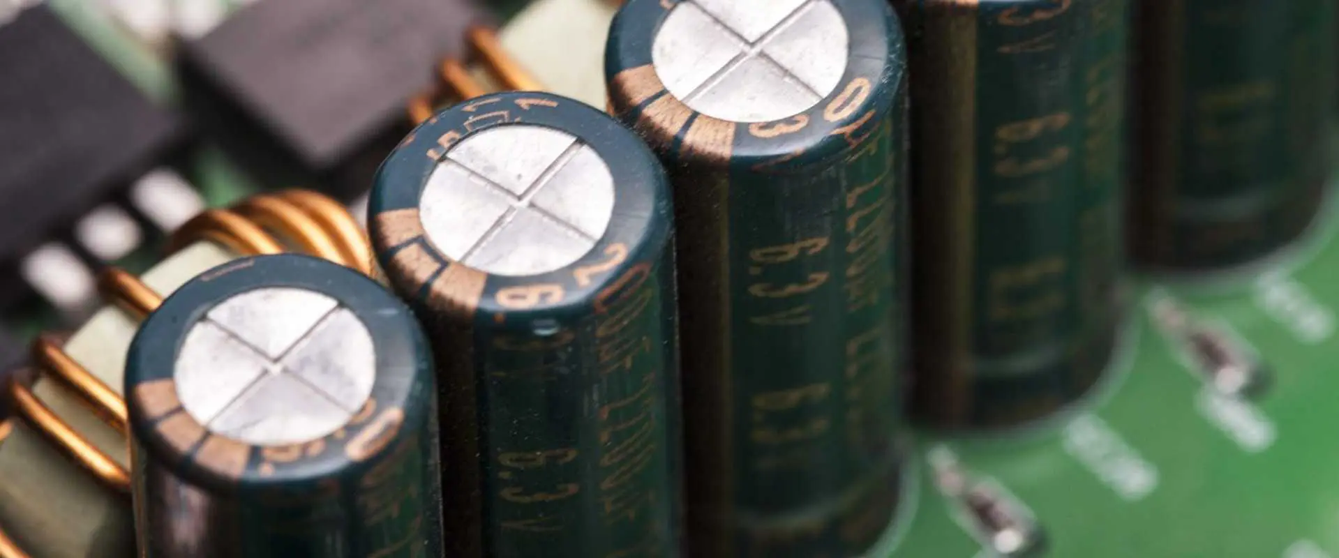
Capacitors are devices that store electric charge and consist of two conductors separated by an insulator or dielectric material. Based on dielectric used, capacitors are classified as ceramic, electrolytic, polyester etc.
Capacitors are used for blocking DC signals, coupling AC signals, filtering, timing and tuning applications. Typical capacitance values range from 1 pF to 1 F.
Inductors
Inductors are coils of wire that introduce inductance and oppose changes in current by inducing a back EMF in the circuit. Inductors are used in filters, oscillators, circuits dealing with radio signals to restrict high frequency signals.
Common types are air core inductors, ferrite core inductors, toroidal core inductors, variable inductors etc. Typical inductor values range from 1 uH to 100 mH.
Transformers
Transformers consist of two electrically isolated coils wound on a ferrite core. They work on the principle of mutual inductance and are used to step-up or step-down AC voltages. Transformers need AC supply and cannot work with DC.
Transformers have no moving parts and are highly efficient. They provide isolation and voltage conversion in a single unit.
Active and passive components are used extensively in various electronic systems and circuits. Here are some of their major applications:
Amplifiers – Use transistors and opamps (active components) along with resistors and capacitors (passive components)
Oscillators – Use transistors or opamps along with RLC components
Power supplies – Use transformer, rectifier diodes, filter capacitors and voltage regulator ICs
Tuned circuits – Use capacitors and inductors along with active components
Digital logic – Use transistors and diodes along with resistors in logic gates and sequential logic circuits
Switching circuits – Use transistors as switches to control power flow
Wave shaping – RC and RL circuits shape waveforms
Wireless transmission – Use inductors, capacitors along with active components in RF transmitters/receivers
So in most electronic systems, active components provide amplification while passive components help in filtering, impedance matching, voltage scaling and wave shaping functions.
Used for amplification, oscillation, switching, control purposes
Used for filtering circuits, wave shaping, impedance matching, voltage scaling
Difference between Active and Passive Components – FQA
Q1. What is the key difference between active and passive components?
A1. The key difference is that active components require an external source of power for their operation while passive components do not require any external power source. Active components can amplify signals while passive components cannot.
Q2. Give some examples of active components.
A2. Examples of active components include transistors (BJT, FET etc.), integrated circuits (Opamps, voltage regulators), vacuum tubes (diodes, triodes etc.), silicon controlled rectifiers (SCRs), optical sensors, etc.
Q3. Give some examples of passive components.
A3. Examples of passive components include resistors, capacitors, inductors, transformers, fuses, wires, cables, connectors, relays, sensors, switches, potentiometers, etc.
Q4. Why are active components generally more expensive than passive components?
A4. Active components are more expensive due to their complex internal structure and fabrication. They require clean room facilities and advanced semiconductor manufacturing processes. Passive components can be mass produced cheaply using simpler fabrication techniques.
Q5. What are the advantages of integrated circuits over discrete components?
A5. The key advantages of ICs over discrete components are – very small size, low cost due to batch processing, high performance, high reliability, low power consumption, improved temperature stability. Discrete components also have higher parasitic effects compared to ICs.
Conclusion
To summarize, the major difference between active and passive components lies in their power requirements. While active components need external power to operate, passive components don’t require any power. Active components are used to amplify and control the flow of current and signals. Passive components are incapable of amplification but are used for filtering, storing energy and limiting current. Both active and passive play crucial roles in electronic systems and circuit design. Understanding their characteristics aids in selecting the right components for specific applications during circuit design and analysis.
SMT has been a preferred choice in the industry to date. Most components in devices feature SMT electronics. In this article, we will discuss everything you need to know about SMT electronics.
To get a vivid explanation of SMT electronics, it is important to know what SMT is. SMT means Surface Mount Technology. SMT designs electronic circuits in which components are mounted on PCBs. SMT electronics are often lightweight. The use of SMT in electronics manufacturing has helped to replace the use of traditional components.
Most electronic devices utilize SMT. This is because of the benefits this technology offers. SMT is an important aspect of electronic assembly. SMT is different from through-hole technology. In SMT, automated machines help to assemble electronic components on the surface of the PCB. This type of technology is very common in the industry.
SMT has been the mainstay in the electronics industry since the late 1980s. Most components in electronic devices feature SMT electronics assembly. It is important to understand how SMT electronics assembly works. Today’s electronic equipment features minute devices. Most consumer electronics are manufactured using SMT.
SMT provides a lot of benefits to users. Since the use of traditional components isn’t easy for PCB assembly, SMT has been a preferred option. SMT is the primary technology for the assembly of PCB in electronics manufacturing.
This technology is now the standard for PCB manufacturing. SMT was invented to make PCB manufacturing easier.
Benefits of SMT Electronics
smt electronics manufacturing
SMT electronics offer a lot of benefits. Generally, SMT has helped in the production of smaller and lightweight devices.
Smaller size
This is one of the most common benefits of SMT electronics. With this technology, it is easy to create small PCB designs. With the use of SMT, it is easy to increase the density of the component on the board. It is very easy to place more components in a smaller space. However, this board still offers the capabilities of a larger board.
This makes it easy to produce smaller and lightweight electronic devices. These days, a very small device can be very complex. The size of a device doesn’t determine its complexity. For instance, some medical devices are very small, yet they are high-performance devices.
SMT reduces the weight of most devices. This provides more opportunities for designers to improve their skills. For example, if drones feature lighter and smaller circuit boards, they will need less power to fly. Reducing the weight of some electronic devices can also help to reduce the cost of shipping. SMT has helped in the production of smaller and lightweight electronic devices.
This is one of the benefits of SMT electronics. This technology offers designers more opportunities to be creative. When it comes to the production of PCB, flexibility is important. SMT helps in the production of rigid-flex and flex circuit boards.
This technology has contributed to the innovation of great designs. In those days, the traditional way of mounting components limited the ideas of designers. These days, the production of advanced electronics has continued to increase.
Lower cost
The ease of assembling these circuit boards helps to reduce costs. When it takes less time to assemble these components on the circuit board, the cost of production reduces in the long run. There is also a cost reduction in terms of the packaging, handling, and delivery of SMT devices. Since SMT requires drilling fewer holes, this makes SMT PCBs more affordable.
SMT electronics can withstand vibration and impact. This is a major reason it is used in high-performance applications.
Easier automated assembly
SMT eliminates the need for custom wire layout, so it results in easier automated assembly. Since human assembly is eliminated, automated assembly is enabled. This also helps to reduce the time required for PCBs production.
SMT electronics also has its downsides despite the benefit it offers.
Vulnerable to damage
Surface mount devices can damage easily. These devices are very sensitive to ESD. Therefore, manufacturers need to handle these devices with much care and caution.
Less power
The power of surface mount device components is less. Not all passive and active electronic components include SMT.
Difficult inspection
It is very hard to inspect components on a surface mount device because of its many solder joints and small size. Also, SMT inspection equipment is very costly.
Difficult to repair
Repairing surface mount electronics can be very difficult. This is because there is a small amount of lead space.
What is the Difference Between Surface Mount Technology and Surface Mount Devices?
Surface mount technology is different from surface mount devices. These two terminologies have confused a lot of people. In this section, we will talk about the difference between these two terms. SMD is one of the components of SMT. A surface mount device is a part attached to a circuit board during the manufacturing of electronics.
SMDs are much smaller than previous components. SMDs utilize surface mount technology. SMT involves the entire process of soldering and mounting electronic components onto a board. These components are surface mount devices.
Surface mount device is ideal for surface assembly on a printed circuit board. It is a small part fixed to a circuit board in electronics production. These devices are much smaller than previous components. Several different packages for passive surface mount devices. But, most passive SMDs are SMT capacitors or SMT resistors.
SMT involves attaching electronic components to PCB’s surface. It uses reflow soldering to weld the surface-mount assembly to the plate. SMT is a common process in the electronics industry. SMT assembly process starts at the design stage. Here, the manufacturer selects different components and uses software packages for the design. The process of SMT assembly includes;
Preparation and inspection of material
You need to prepare the PCB and SMC. After this, ensure you check for any defects.
Prepare the template
In solder paste printing, the steel mesh helps to fix a position in solder paste printing. The design position of the pad on the circuit board determines the steel mesh production.
Printing the solder paste
The solder paste printer helps to apply the solder paste to the solder pad on the circuit board. This machine uses a scraper and a template to apply solder paste. Solder paste printing is a common method of applying solder paste. However, spray printing is another method that is becoming more popular.
Spray printing is commonly used in sub-contract departments. Here, you don’t need a template. You can use a mixture of tin and flux to connect SMC and solder pads.
Inspection
You can include automatic detection to most solder paste presses. But, this process can consume more time depending on the PCB’s size. You can use a separate machine to achieve this. The spray printing machine uses 3D technology to detect more problems. The solder paste printer’s detection system uses 2D technology.
Components location
After inspecting, the next stage is the placement of components. A clamping nozzle or vacuum helps you to remove every component from the package. Then, the visual system checks them and places them in a programmed position.
Reflow soldering
The next step here is to transfer the PCB assembly to the reflow welder. The welder then heats the assembly to a good temperature. The electric welding connections form between the circuit board and the component.
Reflow soldering is one of the less complicated stages in the SMT assembly process. However, the correct reflux profile ensures acceptable solder joints that don’t damage the assembly.
Cleaning and final inspection
After you have wielded and checked the board for any defect, clean the board. Repair any defects. This stage is very important in SMT assembly.
Surface mount technology is common in the electronics industry. This technology helps in the production of electronic circuits. SMT has grown so popular in the electronics industry due to the benefit it offers.
Since this technology helps in the production of smaller devices, it is a preferred choice among engineers. SMT also provides improved performance. With the introduction of SMT, the manual invention is not needed in the assembly process. It is very difficult to join wired components. This is because you need to pre-form them before fitting them into drilled holes.
SMT is ideal in the production of home devices and other electronic components. Most lightweight and small electronics feature surface mount technology. SMT is used in the production of medical, military, automotive, and industrial devices.
In terms of reliability, cost, weight, and volume, SMT is the best option. This technology has helped to improve the performances and life spans of electronic devices. Surface mount technology is used in the applications below;
Consumer electronics
SMT is the commonest method of mounting components on circuit boards. This technology helps in the production of tablets, computers, and smartphones. Since it is lightweight, it is the best option for the production of most consumer electronics. SMT allows for the production of smaller devices.
Medical devices
The introduction of SMT in the electronics industry has led to improvement in the production of medical devices. Surface mount technology has proved to be reliable for medical devices. Devices such as monitors, imaging systems, and infusion pumps feature SMT.
SMT has contributed to the production of more advanced and smaller electronic devices. Most medical devices today feature surface mount technology.
Industrial equipment
SMT technology is used in the industrial sector. This sector makes use of high-performance industrial devices. Electrical components help to power equipment in manufacturing centers and other industrial environments. Circuit boards in the industrial sector have to be durable enough. These PCBs feature properties that help them tolerate extreme temperatures.
To date, surface mount technology is a popular technique in the PCB industry. This technology was introduced into the market in the 1970s. SMT has continued to be the mainstay of modern electronic assembly. Since its advent, it has replaced wave soldering assembly.
Surface mount technology is a revolution of the electronic assembly technology. One can say this technology has been a global trend in printed circuit board assembly. Therefore, it has led to a great development in the electronic industry.
The transformation in the electronic industry is attributed to the advent of SMT. More so, the use of SMT indicates the scientific progress degree of a nation. This technology made electronic components to be highly reliable and lightweight.
Almost all devices in today’s world feature surface mount technology. SMT has helped manufacturers to design small electronic devices that can be used in high-performance applications.
Techniques of SMT
SMT has different types of techniques. These techniques can be classified according to assembly and soldering method.
Assembly method
SMT techniques are categorized into double-sided mix assembly and single-sided mix assembly.
Soldering method
Here, SMT are in two categories, which are: Wave soldering and reflow soldering
Some elements that influence the quality of soldering include:
Several factors affect the quality of reflow soldering. These factors are explained below;
Technological requirement for setting temperature curve for reflow soldering
Soldering quality depends on temperature curve. Before 160 degree Celsius, one should control the rising rate of temperature to 2 degree Celsius per second. PCB and electronic components suffer heat when the temperature increases too quickly. This damages components and leads to PCB deformation. Meanwhile, that kind of high solvent evaporation speed makes metal powder spilled with solder ball.
The peak value of temperature should be more than melting point of alloy by 40 degree Celsius. A low peak value of temperature can result in incomplete soldering without producing a metal alloy layer. Sometimes, solder paste can fail to melt. A long reflow soldering time or high temperature value can make metal alloy extremely thick.
Soldering paste quality’s effect on reflow soldering technique
Statistics revealed that printing technique related problems account for 70 percent of surface assembly quality issues. During the printing process, edge subsiding and insufficient printing cause disqualification. PCBs having these kinds of defects need to receive work. Certain inspection standards should be according to IPC-A-610C.
Technological requirement for SMDs
Some techniques need to meet certain requirements to achieve ideal mounting quality. Some of these requirements are accurate positions, ideal pressure, and accurate components. Certain inspection standards should working in accordance with IPC-A-610C.
Features of SMT Electronics
The through hole technology requires inserting pins of components into through-hole vias on PCBs. THT features high weight and large volume which make it difficult to assemble. Surface mount technology provided solutions to the issues of THT. SMT includes the following features;
Strong vibration resistance
Low rate of defect for soldering points
Electromagnetic and RF interference reduction
High assembly density
Automation accessibility
Surface Mount Electronic Components and Types
In terms of functions, SMT is similar to components for THT. However, the two techniques are comparatively better when it comes electric performance. Package types, use of components, and lead configurations make it hard to form a product.
For instance, they should tolerate high temperature and well-soldered to help products meet requirements. Surface mount technology has continued to evolve. This has helped to resolve several problems that arise from components standardization.
There are two major types of surface mount electronic components. They are passive and active surface mount electronic components.
Passive surface mount electronic components
Passive components don’t offer additional power benefit to the device. The shapes of these components are either cylindrical or rectangular. The weight of these components is much lower than their counterparts.
Surface mount capacitors and resistors are available in different sizes. This helps to meet the demands of different applications in the industry.
These networks serve as replacements for a group of discrete resistors. It is a combination of different resistors. The body dimensions may change. Most times, they are available in 16-20 pins.
Surface mount discrete resistors
These discrete resistors are in two types. They are thin film resistors and thick surface mount resistors. Thin film resistors feature resistive element on a ceramic base. They also have soldered terminations on their sides. Thick surface mount resistors require screening a resistive film on an alumina surface. You can then get the resistance value by examining the variance between the compositions of resistive paste.
For this type of component, they are various categories.
Ceramic leaded chip carriers
Ceramic leaded chip carriers are in postleaded and preleaded formats. The user fixes the leads to the leadless ceramic chip carriers’ castellations in the postleaded chip carriers. In the preleaded chip carriers, the manufacturer attaches the Kovar leads or copper alloy. The dimensions of leaded ceramic packages are similar to plastic leaded chip carriers.
Leadless ceramic chip carriers
These carriers don’t have any leads. They only feature castellations that offer shorter signal paths. These paths enable higher operating frequencies. Based on the packages’ pitch, the leadless ceramic chip carriers are in different categories. The commonest category is 50 mil. Others can be 20, 25, and 40 mil.
SMD Active Components for SMT
Plastic SMD packages are commonly used for nonmilitary applications. While ceramic packages have their own issues, plastic packages can be a better option.
Small outline transistors
Small outline transistors or SOT are four or three lead devices. The four lead devices are SOT 143 while the three lead SOT devices are SOT 23. These packages are suitable for transistors and diodes. SOT 89 and SOT 23 packages have become popular for surface mounting small transistors.
Small outline J packages
This package is like a combination of PLCC and SOIC. Small outline J package provides the benefits of both.
Small outline integrated circuit
This integrated circuit has leads on 0.050” centers. SOIC are suitable for housing several small outline transistors. Small outline integrated circuit needs careful handling to avoid any lead damage. SOICs have different body widths. The 150 mil is the one with less than 16 leads. The package with more than 16 leads is the 300 mil.
These packages feature a greater number of leads and finer pitch. They also have land pattern designs and thinner leads.
Plastic leaded chip carriers
This is a better option to ceramic chip carriers. These leads absorb the solder joint stress which helps to prevent any solder joint crack.
Ball grid array
The ball grid array is a package without any leads. BGAs are available in ceramic and plastic types. BGAs are ideal for self alignment when there is reflow.
Surface mount technology assembly is suitable for manufacturing smaller and lightweight electronics products. SMT assembly is a great technique for complex electronic devices. SMT is ideal for use in several applications. This technology is widely used in the electronics industry.
Does SMT require the drilling process?
Yes, SMT requires the drilling process. But, fewer holes are drilled into the PCB. This helps to reduce the cost of handling and processing. Through-hole technology requires more holes to be drilled. Therefore, SMT is a better alternative.
Conclusion
SMT electronics are the commonest technique in the electronics world. SMT has helped in the production of small, and yet complex devices. It is no doubt that most devices today feature surface mount technology. The advent of SMT has led to the production of better and more effective electronic devices. SMT is now the order of the day in today’s electronic industry.
The Xilinx XC7K410T-2FFG676i FPGA belongs to the Kintex-7 family and is available in different speed grades such as -2L, -1L, -1, -2, and -3. The -3-speed grade is with the highest possible performance. Whereas, -2L speed grade is preferred to be utilized for applications where requirements for low maximum possible static power are required. This device is capable of operating in low core voltages. The industrial temperature devices of -2L are capable of operating at VCCINT to be 0.95V only. The extended temperature devices of -2L can perform at VCCINT=0.9V and sometimes at 1.0V too. The devices of -2LE speed grade can perform at VCCINT=1.0V. The devices of -2LI can operate at VCCINT=0.95V. The specifications for -2LI devices are almost the same as that for -2 devices with an exception of some points. The dynamic power, static power, and speed consideration are reduced for -2LE devices when these operate in the VCCINT to be 0.9V. The military temperature devices -1L are having the same speed consideration as that for -1 military temperature devices.
The Xilinx XC7K410T-2FFG676i AC and DC features are divided into temperature ranges of commercial, expanded, industrial, military, and extended. An exception is considered for the operating temperature range, apart from that all of its AC and DC characteristics and electrical parameters are similar for a specific speed grade device. For example, characteristics of timing for devices of -1 speed grade are the same as for -1 devices of commercial temperature speed grade. Nevertheless, a selected range of devices or their speed grades is available for every range of temperature. For instance, -1Q is available for the Kintex-7 XA family and -1M is available only for the Kintex-7 defense-grade family.
Absolute Maximum Rating of Xilinx XC7K410T-2FFG676i
If any stress or force is applied to the Xilinx XC7K410T-2FFG676i device beyond mentioned absolute maximum rating may or may not result in damaging the IC forever. Furthermore, constant and regular exposure of the device to its absolute maximum ratings may also result in its non-reliable performance. For the device, its lower absolute voltage specifications are also always applied. The maximum possible limit of the device applies to DC signals and its minimum and maximum overshoot and undershoot specifications for AC voltages must be considered. Following thermal and soldering guidelines are also important to get the maximum benefit out of the device.
Recommended Conditions of Operation
There are certain recommended operating conditions for Xilinx XC7K410T-2FFG676i which must be followed such as the voltages applied must be relative to ground. For designing the system of power distribution, pin planning, and PCB design guides must be consulted. The VCCBRAM and VCCINT must have a connection to the same point of the same supply. The data of configuration is retained in the device even if VCCO has dropped to 0V. The supported VCCO ranges of the device comprise 3.3V, 1.2V, 2.5V, 1.35V, 1.8V, and 1.5V. The specifications for lower absolute voltages must also be followed for the device. For each bank of the device, the current must not exceed 200mA. The VCCBATT is only needed when bitstream encryption is utilized. In case of the battery is not utilized, then VCCBATT must be connected to VCCAUX or GND. A filtering circuit is required for every voltage range that is listed and for the data rates above 10.3125 Gb/s, VMGTAVCC must be equivalent to 1.0V to consume less power. Furthermore, for less power consumption, VMGTAVCC must also be 1.0V for the entire frequency range of CPLL.
Power Supply Sequence of Xilinx XC7K410T-2FFG676i
There is a specific powering ON sequence required for the Xilinx XC7K410T-2FFG676i that is starting with VCCINT, followed by VCCBRAM, VCCAUX, VCCAUX_IO, and ends at VCCO. This is how the device can minimum possible drawl of current for ensuring the inputs/outputs to be at 3-state during power ON condition. The power OFF sequence is in reverse to that of the power ON condition. In case if VCCBRAM and VCCINT are having similar voltages that are recommended then both of them could be powered through the same supply. Now, if the VCCO, VCCAUX_IO, and VCCAUX are having similar voltages that are recommended then both can be in power ON status through the same supply and can also be ramped together.
The Measurements of Output Delay
The delays at the output of the Xilinx XC7K410T-2FFG676i device are measured with minor output traces. The device is making use of a standard termination for testing. The propagation delay of traces is considered distinctly and then deducted from the measurements that are finalized. This is why the measurement mechanism is not included in the generic test setup for the device. Different parameters such as VMEAS, VREF, CREF, and RREF are describing the testing conditions of every input/output standard. The precise prediction for the propagation delay through a given application is being obtained through the simulation in the IBIS tool. The simulation is conducted in a specific way such that the output driver of a specific choice is to be simulated into a generalized test setup through the use of various values. The VMEAS is to be recorded. The output driver must be simulated into traces of PCB and then loaded through the utilization of an appropriate model at IBIS or with the value of capacitance representing the load. After that VMEAS must be recorded.
VCCINT is the specified voltage for all speed grades of the device Xilinx XC7K410T-2FFG676i. the devices of -1 speed grade are requiring an internal data width of 4 bytes for its operation beyond 5.0 Gb/s. The device of -2LE speed grade is requiring an internal data width of 4 bytes for its operation beyond 3.8 Gb/s. However, the data rates for the devices are not available among 8.0 Gb/s up to 9.8 Gb/s. The line rates that are beyond 10.3125 Gb/s, the VMGTAVCC is to be 1.05V at the nominal case.
Specifications of XADC
The gain and offset errors are eradicated by enabling the XADC gain through the calibration feature of Xilinx XC7K410T-2FFG676i. However, the values are only specified after the feature is enabled. In case of a variation in reference voltages from any of its nominal values VREFN is to be OV and VREFP is to be 1.25V to result in a slight change from the ideal transfer function. This is also supposed to impact the precision of the measurements of internal sensors such as power supply and temperature.
The Xilinx-7 FPGA series Xilinx XC7K160T-2FFG676i consists of a total of 4 families namely spartan-7, Artix-7, Kintex-7, and Virtex-7. This FPGA is manufactured based on higher-end technology with low power consumption capabilities and an unmatched increase in the performance of the system. This IC has a state-of-the-art FPGA logic that is grounded on a lookup table of 6 inputs which may be configured in the form of distributed memory. With its integrated FIFO logic enabled 36Kb block RAM, it can do data buffering on-chip. The rapid speed serial connectivity along with integrated numerous gigabit transceivers that range from 600Mb/s till 28.05 Gb/s offers a dedicated mode for low power consumption. The DSP slices have a total of 25×18 multipliers along a high-tech pre-adder for filters, an accumulator of 48 bits. Xilinx XC7K160T-2FFG676i has outstanding clock management tiles, a mixed-mode clock manager, and a phase-locked loop for greater accuracy and less jitter.
Electrical Characteristics of Xilinx XC7K160T-2FFG676i
The single-ended outputs of the device are utilizing a traditional CMOS pull/push structure at its output that drives in HIGH mode at VCCO and a LOW mode towards GND. This can also be put into a HIGH-Z state. The designer of the system is capable of specifying output strength and its slew rate too. Its input is always in active mode; however, it is often ignored whenever its output is active. Every of its pin may or may not have an optional pull-down or pull-up resistor. Most of the pairs of pins of Xilinx XC7K160T-2FFG676i could be configured in the form of a differential output or input pairs. The input pair of pins can also be ended along 100 Ohms resistor. Entire families of this device are supporting differential standards that go beyond differential HSTL, BLVDS, differential SSTL, LVDS, and RSDS. Every of its input/output is supporting standards of memory input/output like differential and single-ended HSTL.
Out-Of-Band Signaling
The transceivers of the Xilinx XC7K160T-2FFG676i are offering out-of-band signaling that is more often utilized for sending lower-speed signals from the transmitter to that of the receiver. Whereas, the higher speed transmission of serial data is not in active mode. This is conventionally achieved at a time when a link is in the form of power-down mode. It can also be achieved when a link is not yet initialized.
Built-in Interfaces for PCI Express Design
There are numerous built-in blocks for various interfaces in Xilinx XC7K160T-2FFG676i such as block for compliance to PCI express base with specifications of 3.0 or 2.1 along with the capability of root-port and endpoint. These blocks are supporting different generations such as Gen1 of 2.5 Gb/s, Gen2 of 5 Gb/s, and Gen3 of 8 Gb/s. There are various high-tech configuration options such as end-to-end CRC error detection, and high-tech error reporting. All of the families of devices i.e., Virtex-7, Kintex-7, and Artix-7 are comprising of an integrated block for the technology of PCI express that has the capability for root port and endpoint. The Xilinx is offering an IP wrapper that is light in weight, easy to utilize, and configurable too tying numerous building blocks for clocking resources, block RAM, transceivers, and PCI express. The designer of the system is capable of having control over numerous configurable parameters such as filtering, decoding register for base address, the clock frequency of reference, interface speeds of FPGA logic, highest payload size, and lane width.
In almost all of the Xilinx XC7K160T-2FFG676i series, the bitstream of FPGA is consisting of sensitive customer IP. This IP is protected with AES technology of 256-bit encryption along with an authentication mechanism of SHA-256 for prevention against illegal design piracy. FPGA is performing decryption while the configuration is in progress through an internally installed battery-enabled RAM. The configuration data could be read back irrespective of having an impact on the operation of the system. Usually, the configuration is known as all an all or nothing operation but in Xilinx XC7K160T-2FFG676i series devices partial support is given to configuration. This feature is powerful and is flexible too allowing users to make changes in different parts of FPGA keeping all other parts in a static position.
Analog to Digital Converter
Xilinx XC7K160T-2FFG676i has an analog to digital converter having numerous features comprising of a 12-bit dual-mode single MSPS analog to digital converter. The ADC is having over 17 user-configurable and flexible analog inputs. There is an option for external reference and an on-chip temperature sensor with ±4°C accuracy. There is non-stop JTAG access to all of the measurements taken by analog to digital converter. Almost all of the devices of the Xilinx-7 family have a built-in analog to digital converter interface designated as XADC. When the XADC is combined with the capability of programming logic, it is capable of addressing a vast range of monitoring and data acquisition requirements.
The XADC of Xilinx XC7K160T-2FFG676i is consisting of a 12-bit single MSPS analog to digital converter having a separate track for holding amplifiers along with an on-chip multiplexer, supply, and thermal sensors. Both of the ADCs could be configured collectively for sampling the two external-input channels of analog mode. The hold and track amplifier are supporting a wide range of analog input types of signals comprising of differential, bipolar, and unipolar types. The analog inputs are capable of supporting signals with a bandwidth of almost 500 kHz at a sampling rate of over 1 MSPS. The possibility of supporting higher bandwidth is also possible through the utilization of a multiplexer at its external side along with a dedicated analog input. The XADC is utilizing an on-chip circuit for referencing optionally. This is eliminating any requirement for an external component in an active state for primary on-chip monitoring of power supply rails and temperature.
The EasyPath-7 is delivering a very fast, risk-free, and simple solution for making reductions in costs for Virtex-7 and Kintex-7 family designs. This is also supporting the same speed grades, packages, and is matching the entire range of Kintex-7 and Virtex-7 specifications when timing and functioning are considered. Irrespective of any requalification and re-engineering, EasyPath-7 is delivering the lowest possible product cost when compared to any other competitor FPGA.
The Xilinx XC7K160T-2FBG484i is a Kintex-7 series field programmable gate array (FPGA) providing high performance, capacity, and bandwidth. This mid-range family balances power, performance and cost for high-end embedded applications.
Key features of this FPGA include:
163,200 logic cells with 6-input look-up tables
On-chip memory of nearly 10Mb
2800 DSP slices for intensive signal processing
High speed transceivers reaching 10Gbps
Advanced power management options
High logic capacity in a space saving BGA package
This article provides an in-depth look at the XC7K160T architecture, characteristics, applications, design considerations, and frequently asked questions surrounding use of this popular Xilinx FPGA.
XC7K160T Family Overview
The Xilinx Kintex-7 family offers high performance FPGAs featuring both high logic capacity and high speed connectivity suitable for wireless, medical, video, and military applications.
The Xilinx Kintex-7 family uses a unified FPGA architecture to efficiently implement designs requiring both advanced digital signal processing and high speed connectivity. It is optimized for applications such as wireless infrastructure, medical imaging, semiconductor test, military video processing, and machine vision.
Key architectural features include:
Configurable Logic Blocks (CLBs): Each CLB contains two slices, each with four 6-input LUTs and 8 flip-flops. LUTs can also be configured as 64-bit RAM or shift registers. There are 32600 CLB slices containing the bulk of the FPGA’s logic capacity.
DSP Slices: 218 27×18 bit multipliers enable intensive DSP functions. Features include cascading, optional pipeline registers, and dedicated ALUs to avoid routing congestion.
Block RAM: Over 9Mb of distributed block RAM provide on-chip data storage. 36Kb blocks support a range of width/depth configurations with ECC options.
I/O: The FPGA offers 550 high performance I/O supporting up to 2800Mb/s. Support for common I/O standards like LVDS, PCIe, SATA, and memory interfaces.
Transceivers: Integrated serial transceivers reach speeds up to 10.3Gbps, with lower power versions at 3.2Gbps. Support various protocols including Ethernet, Interlaken, and PCI Express.
Clock Management Tiles (CMT): 10 CMTs provide clock synthesis, conditioning, and jitter filtering.
This combination of high capacity, high performance blocks makes this an optimal FPGA for advanced embedded systems.
XC7K160T-2FBG484i Characteristics
The XC7K160T-2FBG484i denotes specific device characteristics within the broader XC7K160T family:
Temperature Range: The 2F version supports an extended 0°C to +100°C industrial temperature range for more demanding environments.
Package: This FPGA utilizes a space saving 23mm x 23mm body size, 1.0mm ball pitch 484 ball grid array (BGA) package. Provides highest I/O density in this device class.
Speed Grade and Power: Designated speed grade -2, with maximum static power rating of 2W. Dynamic power consumption is device dependent but less than 10W total.
Configuration: SRAM-based which loads programming from external memory on power up. Remote system update capability.
Part Marking: Xilinx’s marking format for this exact device prints as XC7K160T FFG484 – 2 along with additional manufacturing codes on the chip top side.
So in summary, the XC7K160T-2FBG484i is the Kintex-7 FPGA with 163K logic cells, packaged in a 484 pin BGA, speed grade -2, extended temperature range, SRAM configured.
Key Applications of the XC7K160T
The Xilinx XC7K160T FPGA fits well in high performance embedded systems requiring a balance of digital logic, signal processing, and high speed connectivity.
Some of the key application areas include:
Wireless Communications: Mid-range logic density supports base stations and infrastructure processing data intensive protocols like LTE. Integrated DSP slices and transceivers are optimized for wireless systems.
Medical Imaging: Ultrasound, MRI, and CT scan systems leverage the FPGA’s ability to process large data sets combined with high speed interfaces.
Video Processing: Surveillance, machine vision, and video conferencing systems take advantage of the XC7K160T’s 1080p video performance and image processing capabilities.
Semiconductor Testing: High pin count, fast data rates, and timing features support automated test equipment for semiconductor production environments.
Aerospace and Defense: Ruggedized designs for mission computing, instrumentation and sensors benefit from logic capacity, reliability and extended temperature range.
Scientific Instrumentation: High performance embedded systems used in research rely on the raw processing power, flexibility, and I/O bandwidth of devices like the XC7K160T.
This FPGA hits the sweet spot for many applications needing a balanced feature set, high performance, and proven architecture.
XC7K160T vs Konkurrenz’s Comparable FPGAs
The Xilinx XC7K160T resides between competing FPGAs from other vendors in terms of density and capability:
So the XC7K160T hits a middle ground between lower cost FPGAs and very high density Stratix/Virtex families. This balanced density, features, and cost make it attractive for many applications.
Engineers should keep several design considerations in mind when working with the XC7K160T FPGA:
Utilization – At 163K logic cells, designs over 100K usage require analysis to ensure timing, power, and congestion goals are met.
Thermal – With 10W max power, proper board airflow or heatsinks are needed. Thermal simulation should be performed.
Decoupling – Numerous power pins require proper decoupling for stability. Plan for bulk and localized decoupling.
ESD Protection – FPGAs are highly ESD sensitive. Robust protection diodes, pads, and handling controls must be used.
Design Flows – Xilinx offers strong tool flows – ISE, Vivado, Vitis – leveraging FPGA optimizations and IP libraries.
Debugging – Plan for debug access through JTAG, internal probes, logic analyzers. ChipScope integrated tools are useful.
Properly planning for utilization, thermal, ESD, debug, and taking advantage of Xilinx design tools ensures success with this FPGA.
How to Get Started with the XC7K160T
Xilinx provides excellent documentation and development kits to jumpstart XC7K160T designs:
Product Specification – Data sheet contains comprehensive technical reference information on the FPGA.
Documentation Navigator – Central area to access device user guides, application notes, white papers, reference designs, and training material.
Kintex-7 GTX Transceiver User Guide – In-depth guide to implementing high speed serial I/O.
Vivado Design Suite – Xilinx’s flagship design environment with FPGA-optimized implementation tools.
KCU105 Evaluation Kit – Full platform to develop and evaluate designs. Includes board, power supply, memory module, cables, and documentation.
Engineers should leverage these resources when starting new XC7K160T-based projects.
Conclusion
The Xilinx XC7K160T-2FBG484i FPGA delivers an optimal balance of high capacity, performance, and features for advanced embedded systems. With 163K logic cells, abundant memory blocks, DSP slices, fast serial transceivers, and dense I/O, this versatile FPGA services a wide range of applications. Engineers require FPGA skills and Xilinx-specific expertise to fully utilize the capabilities. Following recommended design practices and using Xilinx development kits accelerates success leveraging the XC7K160T in next generation systems.
Frequently Asked Questions
What are the main differences between Kintex-7 and Virtex-7 FPGA families?
Key differences:
Density – Virtex-7 offers up to 2M logic cells, significantly higher than Kintex-7
Performance – Virtex-7 clock speeds, DSP slices, SERDES are faster
Cost – Virtex devices are most expensive, aimed at top performance
Power – Virtex max TDP up to 30W, Kintex-7 just 10W
Package – Virtex utilizes high-pin BGA packages, Kintex-7 more compact
Certification – Virtex has more rigorous qualification for aerospace/defense
So in essence, Virtex-7 is very high performance while Kintex-7 balances capability and cost.
What are the most important specs for evaluating an FPGA?
Key specifications include:
Logic cells – Determines capacity for digital logic and routing
Block memory – On-chip data storage avoids external memories
DSP blocks – Enable high throughput arithmetic operations
Maximum transceiver speed – Essential for high speed interfaces
Package footprint – Impacts board layout and routing
Temperature range – Industrial grade required for some applications
Static power – Lower power extends battery life
The requirements depend on the target application of the FPGA.
What are the easiest ways to get started with FPGA development?
Recommendations to begin FPGA development:
Use vendor evaluation kits – These provide full out-of-box development platforms
Download design tools – Take advantage of vendor tool ecosystems with optimizations
Follow board user guides – Accelerate learning proper implementation
Run demo projects – Modifying examples is faster than new designs
Take online training – Tool specific and FPGA courses shorten the learning curve
Engage tech support – FPGA vendor FAEs can mentor new users
Jumping right into tools, kits, and examples gets new FPGA developers productive quickly.
What types of designers work with FPGAs?
Typical designers using FPGAs include:
Digital logic designers – Implement logic gates, state machines, algorithms
Hardware engineers – Interface FPGAs to processors, memory, converters
Embedded software developers – Program the integrated soft processors
DSP engineers – Develop complex signal processing blocks
PCB layout designers – Layout, route, and debug FPGA boards
Systems engineers – Manage IP selection, partitioning, co-design
Application engineers – Map product features to optimized FPGA logic
FPGAs therefore require multi-disciplinary systems expertise to properly apply.
What makes Xilinx FPGAs unique?
Some unique advantages of Xilinx FPGAs:
Large ecosystem of third party IP libraries
Long history as the pioneer in FPGAs
Unified, regular architecture for efficiency
Advanced tool suite with unique features
Highest performance transceivers
Comprehensive product portfolio
Wide range of development kits and boards
Strong integration between software and hardware
These factors together provide compelling benefits versus competitors.
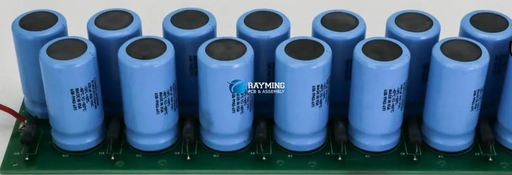
There can be discrete capacitors present along with the PCB capacitor. This may function as capacitors that are lumped. This is suitable because it can be used in creating a system of distribution for your top-quality design.
What is a PCB Capacitor?
Printed circuit boards can function like capacitors. This is because capacitors could be composed of two objects made of metal, put apart by a material that is non-dielectric. Therefore, combining PCB components, pads, pins, and tracks, should transform into a capacitor that will be able to destabilize frequency oscillation.
Asides from this, power and grand planes offer the necessary decoupling capacitance. You can even utilize capacitors at your PCB’s edges. You only need to get two good copper planes. This would serve as capacitors. Then we can go ahead to get discrete capacitors coupled with the capacitor of the PCB. This may function like lumped capacitors, which you’ll utilize in creating a system for distributing your design.
The effectiveness of your design is dependent on some factors. This includes how the decoupling capacitors affect the printed circuit boards. Typically, this plan comes with a top and bottom layer located on the chip’s sides. You connect the vias to the ground and the power plane. The connection of the full capacitors must be done to the ground plane (unbroken) due to the fact that it has some benefits.
Their impedance level is usually the lowest. Unfortunately, if you are searching for signals of high frequency, the arrangement may fail to work. You must have a good layout. This ensures that routing doesn’t find its way into some other movements. Therefore, it is very necessary that your design features two-layer boards.
Non PCB Capacitor
In 1979, PCB capacitors were banned. This means that the manufacturers had no choice but to have something to replace it. This is the Di2-Ethylhexyl phthalate. The dielectric fluid can be seen in non-PCB ballast capacitors. Presently, there is DEHP in about one-quarter of capacitors.
The Role Embedded Capacitors Play in PCB Design
circuit board capacitor
Capacitors work in a special way. You can easily construct one by making use of aluminum foil sheets. Get two of these sheets and separate them using a shopping bag made of plastic. Next, connect the foil beneath the earth ground to the DC power supply’s negative terminal, and then connect the upper aluminum foil to the positive terminal of the power supply. Raising the voltage led to both aluminum foil plates to attract each other noisily.
The capacitors that we make use of in our printed circuit board designs are usually different compared to the capacitor built in any student’s classroom. Before you design the circuit boards, you must know the different properties of the different types of capacitors. This will help in the planning, as well as the design.
If you are working with surface mounted and through-hole designs, you can choose capacitors using the design libraries. This choice is made based on the combination of different attributes, which includes rated voltage, nominal value tolerance, dielectric type, temperature coefficient, and capacitance.
Through-hole mounting has assumed a secondary status to the surface mount technology. However, drilling of holes and the securing of the component leads radially or axially via the board, will add some value for some specific applications. Industrial, aerospace, and military applications need reliability whenever components are subjected to environmental and mechanical stress. The types of THM capacitor are ceramic discs (non-polarized), plastic film, silver mica, coupled with tantalum and polarized electrolytic types.
The surface mount (SMT) type of capacitors do not need hole drilling through the layers. They will also mount to the PCB’s surface directly. Through-hole leads are replaced by the vials, which permits a conducting connection between the circuit board layers. The SMT capacitors mount to the two sides of the board. They also have small packages compared to the Through-hole mounting (THM) capacitors. The types of SMT capacitors include multilayer ceramic, tantalum, mica, electrolytic, and film capacitors.
Embedded Capacitors, Signals, and Circuit Boards
Today, well-known capacitors from history have taken up major roles in surface mount technology PCBs. Looking at the few capacitor types available explains how the capacitor technology has developed from the past till today and has also made an impact into the PCB design future.
There are several benefits of surface mount capacitors. These include low spurious inductance, automated assembly, and small size. Similar features were seen with older through-hole mounting types of capacitors. This offers many advantages for designers of PCB that work with SMT.
Embedded Circuit Boards and Components Now
Materials for embedded capacitance are made of a dielectric material that is usually very thin. Also, they are sandwiched between two copper layers. During the process of manufacturing, an epoxy material coating helps in laminating the copper foils. Capacitors that are embedded into the flex or rigid PCB substrate below an integrated circuit’s pin, usually have their electrical paths very short, which reduces the parasitic inductance and capacitance, and minimizes the EMI.
Due to the increase in capacitive density, the embedded capacitors could become a decoupling capacitor. Therefore, it can ensure the removal of capacitors that are discrete. When you combine these capabilities with the size reduction, embedded capacitors have become very valuable for handheld, medical, computing, and telecommunications equipment.
Smaller footprints for products have become very important. This importance has begun a revolution in the technologies of capacitors. The next step has to do with high density development, solid ultra-thin aluminum capacitors, which provide stability in high-temperature, high-voltage applications, as well as the circuits powering them.
One other electrolytic ultrathin supercapacitor functions for RF applications and microprocessor operating with low power. Designed as components that are embedded, the supercapacitors will offer a very long power life. This is to prepare for the next generation internet of things (IoT) devices, coupled with resisting shock and vibration.
These capacitors are dielectric in nature, and are made from ceramic materials. Ceramic capacitors usually have small values as their capacitance. This value usually ranges between 1F to 1µF. Their capacitors have great frequency response. Also, they are never prone to the effects of parasites.
Ceramic capacitors of class 1 provide low loss, accuracy, and high stability. Their nominal value tolerance can fall within the 1% range. Ceramic operators of class 2, come with greater capacitance values. However their thermal stability is lesser and their nominal value tolerances are less sensitive. Ceramic capacitors operating with large power feature a maximum capacity of 100µF. Also, they can deal with much higher voltages, which could get to as high as 100 kV.
MLCC – Multilayer Ceramic Capacitors
These capacitors account for a large number of capacitors utilized on the surface mount printed circuit boards (PCBs) of today. All MLCC are made up of silver palladium that are interleaved or silver electrodes that are plated with nickel covered with tin (plated) and then interweaved. The dielectric type used when manufacturing the MLCCs has an effect on thermal stability and capacitance.
Capacitors that have a calcium zirconate or titanium oxide dielectric feature a lower capacitance. They also have some thermal characteristics that are very stable. When working with PCB applications involving high-frequency circuits that work with time constant, choose the high-temperature, low capacitance MLCC. The MLCCs having Barium titanate dielectric provides the high capacitance required for power supply decoupling and smoothing.
Note that the MLCCs’ high capacitance balances against the dielectric’s properties. Over time, there’s a change in the Barium titanate dielectric with the input of voltage.
MLCC capacitors feature low resistance. Due to this, they encounter few issues with the generated heat by resistance. Also, the capacitors offer a great ripple resistance.
Mica Capacitors
They function like ripple filters and decoupling capacitors in power conversion, coupling, time constant, and resonance circuits. Mica capacitors are built from mica sheets, with both sides being coated with metal that is deposited.
SMT and THM mica capacitors offer great stability, reliability, and precision. Their nominal value tolerances are either +-1%, +-2%, or +-5%.
Plastic Film Capacitors
This type of capacitor utilizes different dielectric materials. These materials segment these components for some specific applications. These include general decoupling, coupling, and filtering. Metalized film capacitors like Mylar, as well as other different polystyrene and polyester capacitors are made up of a thin metal layer, which is deposited in a plastic film connecting each lead. The film foil type of capacitors like the PTFE –polytetrafluoroethylene capacitor utilizes plastic films in separating the two electrodes made with metal foil.
FCN Capacitors
This type of capacitor features a metalized non-inductive polyethylene naphthalate film construction, which offers a similar frequency characteristics and stable temperature that are found in the traditional capacitors made of polyester film. The FCN capacitors usually have low ESR. This is why it yields a high-frequency and superior performance.
Due to this, FCN capacitors function for output filtering, power supply input, signal coupling, and EMI filtering.
Type FCP Polyphenylene Sulfide (PPS) Stacked Metalized Film Capacitors
This type of capacitor has high values for their capacitance. Also, over a wide range of temperatures, their high-frequency response is excellent. Just like FCP capacitors, the Type FCA film capacitors (acrylic) provides values of high capacitance couples with a much better high-frequency filtering. Their bus noise attenuation is excellent too. FCA capacitors are composed of alloy terminals plated with copper and metalized resin film having stacked layers that are non-inductive.
Tantalum Capacitors
These capacitors utilize a thin oxide file on tantalum, which is used like an electrolytic. As the oxide layer covers the tantalum anode, and functions like the dielectric, there is a conductivecathode that envelopes the anode and the dielectric.
Though tantalum capacitors lack the present capacity seen in the aluminum electrolytic capacitors, the tantalum capacitors provide stability, endurance, and a high capacitance between 1µF and 100µF. SMT tantalum capacitors offer similar properties. This also includes a wide range of operating temperatures.
Aluminum Electrolytic Capacitors
This type of capacitor provides a much higher capacitance compared to other types of capacitors. However, their values for nominal tolerance are very wide. Higher values for higher capacitance make way for ripples to be smoothened by electrolytic capacitors whenever it is utilized in power supplies, and they function like coupling capacitors.
As a result of the wide values for tolerance as well as an increase in equivalent series resistance with frequency, the electrolytic capacitors don’t work with high frequencies. Surface mount electrolytic capacitors provide high temperature stability, low impedance and high capacitance.
Asides from this, these SMT electrolytic capacitors can resist vibration properly on non-stationary PCBs – printed circuit boards.
How do Capacitors Work?
capacitor on pcb
Capacitors are well-known passive components found in circuits. They are similar to the resistors. Capacitors help in storing electrical charge. They also offer different options. This depends on the design of a circuit. The capacitance has to do with the measure of the energy or charge, which can be carried by the capacitor.
When capacitors are in their basic form, they are made of two plates, with an insulator between them. This insulator is the dielectric. Capacitors are of different types. They are composed of different dielectric materials, and can be utilized for several purposes.
The measurement of capacitance is in Farads. This unit is a fairly large one. This is why it is used generally in microfarads or picofarads. Also, capacitors may also be non-electrolytic or electrolytic. The former may be connected in whatever direction possible in the circuit. For the electrolytic capacitors, you have to install them on the circuit in the right orientation. One of the leads is positive, while the other is negative. The placing of the electrolytic capacitors may not allow your circuits to perform properly. It may even make them pop.
Capacitors may have different applications. One of their critical roles can be found in digital electronics. Here, they protect the microchips from any noise. Due to the fact that the whole charge they carry can be dumped quickly, often they are utilized in lasers and flashes coupled with capacitive sensing and circuit devices. Circuits having capacitors usually display behaviors that are dependent on frequency. This is why they can be utilized on circuits, which amplifies some frequencies.
You can add capacitors either in parallel or in series, just like resistors. However, the calculation is the direct opposite of that of the resistors. The connection of components in series has one node in common. Also, both nodes are shared anytime the connection is in parallel. The resistors connected in series should be added together, if you want to get the total value of the resistance. Also, capacitors having parallel connection should be added, if you need the total value of the capacitance.
Selecting Capacitor Components for your PCB Design
In this section, we will take you through those things you must consider to select electronic components such as capacitors during the designing of your printed circuit board.
New PCB designers will always find it as a challenge when choosing the right electronic components. Choosing these components inappropriately could cause a malfunctioning, a total failure, or an undesired operation of your printed circuit board.
Depending on the component type, there are some important parameters that designers of PCB should consider when choosing the component during the design stage. This section takes you through important consideration for choosing the main electronic components.
How to Choose Capacitors
Capacitors are utilized in different circuits. Choosing the component of your capacitor for your PCB design using just the value for the capacitance is not usually enough in the majority of applications. Just like the resistor components, the capacitors also possess tolerance factors. There is a variation in a capacitor component’s actual capacitance. This is based on the process of manufacturing, aging, DC biasing, and the operating temperature.
Therefore, the tolerances of the capacitance must be considered when choosing the component for your capacitor. The variation in price between the high and low tolerance capacitors also varies considerably. However, if price isn’t an issue for you, then we advise that you choose a capacitor having a tolerance below 10%. For the majority of low power circuits, having 10% or even 20% as tolerance is sufficient.
What Value of Capacitance will you get?
Damage could come to your capacitor if there is a stress on voltage or the voltage is higher than expected. Most times, capacitors are connected in parallel, either to an output, a sub circuit, or a circuit. The expected drop in voltage across your capacitor should be calculated or known. We recommend that your voltage buffer should be 50% over the expected drop in voltage. This means that, if your expected drop in voltage across your pcb capacitor is 10Volts, then you should choose a capacitor having a 15 volts rated voltage or more.
Lifetime expectancy or the capacitor life can be defined as the time period at which the capacitor remains healthy, and offers capacitance just the way it is designed. It is clear that this is critical, most especially for an electrolytic capacitor. A capacitor’s lifetime under conditions of normal operation is usually given on the product’s datasheet, by the manufacturer.
The capacitor’s temperature for operation ranges. This should be seen just like resistors. Based on the application type, ripple current, and the ECR value, the frequency of operation has to be viewed for designs that are advanced.
Tips on How to Place your PCB Bypass Capacitor
Placing your bypass capacitor could be a very critical phase throughout the process of designing your printed circuit board. Failing to place them the right way could cause a negative performance. Another critical situation is when you have very few capacitors for some components. Whenever cases like this arise, you should communicate the information to the engineer. This will make them update the schematic.
Know whether the components should be placed on the board’s bottom side
When many capacitors having different values are given to a supply pin on an integrated circuit, then the capacitor with the lowest value should be placed very close to your device pin.
Larger tantalum and non-polarized capacitors has to be placed close to the device or pin from the lowest to the highest value.
Devices having many power pins should have one or more bypass capacitors per power pin.
Make sure you check the schematic anytime you are placing a bypass capacitor due to the fact that they are usually logic input pins ‘tied high’
The disposal of non-PCB capacitors usually requires user’s compliance with the regulations of the federal government, which governs the disposal. Already, a document is available, which presents guidelines to the scrap yards that reveals how this is done.
Crushing and shredding can no longer be used as an alternative. This is because it will contaminate the area where you are doing this. Due to this, removing and storing non-PCB capacitors helps in reducing and preventing you from violating the requirements.
Requirements for Disposal
Alternatively, you can dispose of the capacitors by reaching out to a transporter to help in transporting the PCB waste. In doing this, you must keep proper records. This includes the quantity of drums, the date you picked the haul, the pick-up date, and the name of the transporter.
Conclusion
Take note that decoupling offers reservoir energy to help in smoothing out voltage anytime a change in the amount of current drawn happens. It is normal for the supply of power to take a little time before it responds to the voltage due to inductance. Therefore, the decoupling cap has to close this gap. To achieve this, make sure it is nearer to the digital chip. Otherwise, the inductance of the lead may disrupt things quickly and therefore make it challenging to be able to get additional current quickly.
The Xilinx XC7A200T-1FBG676C belongs to the Artix-7 family of low-cost, low-power FPGAs built on 28nm high performance, low power (HPL) process technology. With 200K logic cells, 220 DSP slices and 16.3Gbps transceivers, the XC7A200T provides an ideal blend of programmable logic, signal processing and high-speed connectivity for demanding applications including motor control, automotive driver assistance systems, software defined radio, video bridging, aerospace electronics and test instrumentation.
This article provides an overview of the XC7A200T architecture, available resources, target applications, design flow and benefits for electronics engineers.
XC7A200T-1FBG676C Overview
The XC7A200T represents the higher capacity end of Xilinx’s Artix-7 family of FPGAs optimized for embedded systems requiring substantial programmable logic resources. Key features include:
200K logic cells based on look-up table (LUT) architecture
220 DSP slices with 25×18 multipliers operating at up to 300 MHz
Up to 16 gigabit transceivers with data rates up to 16.3Gbps
High speed DDR3 external memories supported at up to 1.6Gbps
1650 maximum user I/Os for expansive connectivity
MGT and LVDS I/O support for high-performance interfaces
Designed for high volume cost-sensitive applications
The 1FBG676 package denotes a 27x27mm 676-pin flip-chip grid array with 1mm ball pitch. This high density form factor provides the ample connectivity an FPGA with 200K logic cells demands.
The Artix-7 family architecture balances high density, high performance programmable logic together with essential integrated processing required for advanced embedded systems.
Programmable Logic Fabric
The core programmable logic fabric utilizes Slice architecture containing LUTs, flip-flops, multiplexers and carry logic as the basic building blocks. Key features:
6-input LUTs efficiently implement logic functions using only a single LUT per slice
Flip-flops for registering logic outputs or implementing shift registers
Arithmetic carry logic for efficient math operations
36Kb Block RAM for on-chip data storage
DSP Slices
220 embedded 18×25 multipliers and 48-bit accumulators enable high-throughput arithmetic and signal processing.
Block RAM
5.3 Mb of distributed 36Kb block RAM provides on-chip data storage with built-in FIFO logic support.
Transceivers
Up to 16 transceivers running at up to 16.3Gbps support high-speed chip-to-chip communications and interfacing.
PCI Express
Two integrated Gen2 PCIe blocks enable direct chip-to-chip communication.
Gigabit Transceivers
Up to 6.6Gbps data rates over differential I/O supports protocols like Ethernet, FibreChannel, Interlaken and Aurora.
XC7A200T Target Applications
The XC7A200T architecture provides an ideal foundation for compute-intensive embedded systems requiring substantial signal processing capabilities:
It is useful to contrast the Artix-7 based XC7A200T against the higher capability Kintex-7 FPGAs:
Programmable Logic
XC7A200T offers 200K logic cells using 6-input LUTs
Kintex-7 provides up to 474K logic cells using 6-input LUTs
Transceivers
Both support up to 16 transceivers operating at up to 16.3Gbps
Memory Interfaces
Both support 1600Mbps DDR3 interfaces
DSP Slices
XC7A200T – 220 slices operating at up to 300MHz
Kintex-7 – Up to 3600 slices operating above 500MHz
Cost
XC7A200T optimized for high volume cost-driven applications
Kintex-7 costs approximately 30-40% higher
For extreme cost-sensitive applications not needing the ultimate logic densities, the Artix-7 based XC7A200T offers a compelling value proposition.
Conclusion
With its high density 6-input LUT fabric, abundant high-performance DSP slices, plentiful RAM and transceivers, the Xilinx XC7A200T-1FBG676C provides hardware designers an extremely capable yet cost-optimized chip foundation for demanding embedded applications including industrial servo control, driver assistance systems, software defined radio, video processing, and aerospace/defense electronics.
For engineers challenged with staying on the cutting edge of connectivity-centric domains requiring both raw processing throughput and flexible programmable logic, the Artix-7 family offers a pin-compatible portfolio scaling from 100K to 350K logic cells to match project needs.
Frequently Asked Questions
Q: What is the Xilinx XC7A200T FPGA?
A: It is a high-end Artix-7 family FPGA with 200K logic cells, 220 DSP slices and 16.3Gbps transceivers, built on a 28nm fabrication process.
Q: What are some key components in the XC7A200T architecture?
A: This includes 200K 6-input LUT logic cells, 220 DSP slices, 5.3Mb of block RAM, up to 16 transceivers, and PCIe blocks, and configurable mixed-voltage I/O.
Q: What are some target applications for the XC7A200T?
A: Motor control, driver assistance systems, wireless infrastructure, aerospace/defense, and video/image processing all leverage the XC7A200T capabilities.
Q: How does XC7A200T compare against Kintex-7 FPGAs?
A: Kintex-7 offers 30-40% higher performance but XC7A200T provides a more cost-optimized solution for many applications.
Q: What tools can be used to program XC7A200T FPGAs?
A: Xilinx’s Vivado, Vitis, and SDSoC tools together enable developing the full system including programmable logic, software, and processing pipelines.