Isola I-Tera MT40: A Low Loss and High Reliable Material for PCB Fabrication

Isola I-Tera MT40 PCB

In todayโ€™s world, the demand for more advanced electronic devices is increasing. Therefore, there is a growing need for high speed PCB materials. Also, the type of PCB material will impact the functionality of a circuit board. In the long run, this circuit board will impact the applications for which they are used for. Therefore, it is important to carefully select your PCB material. This article will shed more light on Isola I-Tera MT40 and what it offers.

What is Isola I-Tera MT40?

Isola I-Tera MT40 is a low loss PCB laminate with great electrical properties. These properties are stable over a wide range of temperature and frequency. Also, this laminate is ideal for most modern RF/microwave and high speed digital PCB designs. This laminate offers a stable dielectric constant. The dielectric constant remains stable between -55 and +125 degrees Celsius.

Furthermore, Isola I-Tera MT40 provides a very low dissipation factor of 0.0031. Therefore, this makes it a cost-effective option to teflon and other RF/microwave laminate materials. Also, Isola I-Tera MT40 PCB material is available in both prepreg and laminate form. It is available in standard panel sizes and typical thicknesses. Therefore, this is a solution package for RF/microwave and high-speed digital multilayer.

PTFE-based laminates often require special through-hole treatments. Isola I-Tera MT40 is a reliable PCB laminate. It requires no special through-hole treatments.

General Properties of Isola I-Tera MT40

Stable dielectric constant

The dielectric constant of Isola I-Tera MT40 contributes to its exceptional electrical performance. This material features a Dk of 3.45. Also, it maintains a stable Dk over a wide frequency range. Therefore, this material is electrically stable.

High glass transition temperature

The glass transition temperature of Isola I-Tera MT40 is 200 degrees Celsius. This is a very high Tg. Therefore, Isola I-Tera MT40 PCB can perform better in applications. Also, this material features high temperature durability. Also, the temperature of the operational environment of this material shouldnโ€™t be above 200 degrees Celsius.

High decomposition temperature

The Tg of Isola I-Tera MT40 is 360 degrees Celsius at 5% weight loss. This means that this material can decompose chemically at 360 degrees Celsius.

Low water absorption

The water absorption rate of Isola I-Tera MT40 is 0.1%. This is a very low rate. This property influences the electrical and thermal properties of Isola I-Tera MT40. Also, this material is ideal for use in humid environments.

Low dissipation factor

The dissipation factor of this material is 0.0031 at 2GHz, 5GHz, and 10GHz. Therefore, this material maintains a low and stable Df over a wide frequency range. This property measures the amount of dielectric losses associated with Isola I-Tera MT40. This material is a low loss material.

Thermal conductivity

The thermal conductivity of Isola -Tera MT40 is 0.61 W/m/K. This material is a good insulator as it doesnโ€™t allow heat to pass through it easily.

Advantages of Isola I-Tera MT40 PCB Material

RoHS compliant

The Isola I-Tera MT40 is RoHS compliant. This means that this material adheres to the standards of RoHS. These standards restrict the use of some harmful substances in PCB materials. Therefore, this material is safe for use in PCB fabrication.

FR-4 process compatible

This material is compatible with the processing of FR-4. Also, it is flame retardant. Therefore, it complies with the UL94 V-0 standard.

High thermal reliability

One of the advantages of Isola I-Tera MT40 is its thermal reliability. This material features properties that contribute to its thermal performance. For instance, it has high Tg value and high Td value. Also, it features low water absorption.

CAF resistance

Isola I-Tera MT40 is an anti CAF PCB material. CAF means conductive anodic filament. It is often caused by the creation of a metallic filament from an electrochemical movement process. CAF has been a major concern in the electronics industry. The occurrence of this problem resulted in the production of anti-CAF material.

Multilayer capability

This material is ideal for multilayer PCB fabrication. Multilayer boards are useful for designs that demand high functional density in a compact space.

Applications of Isola I-Tera MT40 PCB Material

This material features a high-speed digital performance. Therefore, it is ideal for hybrid PCB construction. Also, it is suitable for use in a wide range of applications.

Aerospace and defense

Isola I-Tera MT40 is widely used in the aerospace and defense industry. This material is thermally reliable. Also, it has a high-speed digital performance. All of these attributes are important in the manufacturing of aerospace and defense devices. Also, this material features a stable Df and Dk over a wide frequency range. This is an important consideration for the aerospace and defense industry.

Automotive and transportation

Thermal reliability is an important consideration for PCB manufacturers in the automotive and transportation industries. The Isola I-Tera MT40 PCB material offers great thermal endurance for PCB used in these applications. There is a need for advanced transportation and automotive safety. Also, Isola provides laminates with great performance in this field.

Networking and communication systems

Bandwidth is a major concern in networking and communication systems. Therefore, Isola I-Tera MT40 play a crucial role in these systems. This material features properties that meet the demands for video and satellite services. Isola I-Tera MT40 is specifically designed for the most demanding systems and environments.

Computing, storage, and peripherals

Isola I-Tera MT40 features high speed digital and high Tg. These features make it suitable for these applications. You will find Isola I-Tera MT40 in servers, routers, and backplanes. This material is specifically designed to meet the needs of high-speed digital applications. Also, this material offers stable electrical properties and ease in processing.

Medical, industrial, and instrumentation

This low loss and highly reliable material supports various medical applications. This material is suitable for use in implantable devices, and imaging systems. Isola I-Tera MT40 features multi-lamination capability and HDI microvia capability.

Conclusion

High reliability and performance are important considerations when choosing a PCB material. Isola I-Tera MT40 is a highly reliable PCB material suitable for different applications. Isola designed the I-Tera MT40 to meet the demands of high density applications. Also, the need for advanced PCB materials keeps increasing. The Isola -Tera MT40 is an advanced PCB material with great benefits.

Chip on Board Assembly: An Effective Solution to Electronics Miniaturization

Chip on Board Assembly

There is now a new packaging method far different from the SMD package technology. The chip on board assembly offers more advantages. Also known as COB, you can find this package in the smallest of all electronic devices. Also, you can find it in applications where there is limited space.

Chip on Board Assembly โ€“ What is it?

Chip on board assembly involves installing bare semiconductor chips on a PCB or substrate. The manufacturer uses non-conductive or conductive epoxy to achieve this. Chips incorporate aluminum wedge bonding or gold ball bonding to achieve electrical connection. There are various semi-sintered epoxy resins for chip-on-board assembly. However, these are for applications requiring superior electrical and thermal conductivity.

Also, manufacturers can connect the chip to the PCB by using flip-chip technology. Chip on board technology directly connects semiconductor to the PCB substrate. This technology incorporates the technique of surface mount technology. However, it is different from SMT. COB assembly involves active devices and high lead count. Also, it doesnโ€™t demand for ceramic external device packaging.

The chip on board assembly mounts the die or microchip to the board. Also, the manufacturer attaches the chip to the substrate interposter. Therefore, a flip chip or wirebonding helps to achieve functional connection.

The flip chip on board employs a chip with bumped bond pads. Therefore, it doesnโ€™t require wirebonding. The chip on the flip-chip on board faces down on the board. Also, it is important to underfill flip-chip to prevent any chemical or thermo-mechanical damage.

Chip on boards with LEDs have made LED lighting more efficient than ever. COB is a method of PCB manufacturing in which integrated circuits (ICs) are directly bonded and wired to a PCB board.

What is the Chip on Board?

This is a bare chip mounted directly on the PCB. After the wires have been connected, a ball of plastic covers the chip to create a connection. The manufacturer wire-bonds the bare chip to the board and pours epoxy resin into it. In addition, chip on board is a great option for miniaturized circuits. It provides a better solution when traditional assembly technology canโ€™t meet the design parameters.

The chip on board assembly comprises three steps. These steps include die mount, wirebonding, and encapsulation of the wires and dies.

Die mount

This involves applying a die attach adhesive to the substrate and installing the die over the die mount. The application of adhesive may include pin transfer or dispensing. Therefore, accurate die placement is important to ensure good die planarity. Also, after applying adhesive, there is a curing process. This process enables the adhesive to achieve its final electrical and thermal properties. Also, the PCB manufacturer must use solvent or plasma cleaning to remove organic contaminants.

Wirebonding

This process involves the use of ultrasonic AI wedge bonding or thermosonic Au ball bonding to connect wires between the substrate and the die. The bond pads of the board and the die must have no defects or contaminants. ย Also, this will help to create reliable and good bonds.

Encapsulation of the wires and dies

In this process, the manufacturer encapsulates the bond and die wires to shield them from any chemical and mechanical damage. Also, this process involves dispensing encapsulant material over the wires and die. However, this encapsulants have to undergo curing.

Advantages and Limitations of Chip on Board Assembly

Pros

The main benefit of a COB is that it minimizes the weight of a circuit. Also, when weight is a major factor, the chip on board assembly is an ideal solution. The advantages of chip on board assembly include:

  • Enhanced protection against reverse-engineering
  • Minimized cost
  • Improved performance as a result of minimized interconnection resistances and lengths
  • Minimized space requirements
  • Shorter time-to-market
  • Greater reliability as a result of heat distribution
  • Wide application range
  • Higher reliability due to small number of solder joint

Cons

  • The chip on board led package features a high maintenance cost and low pass rate.
  • High manufacturing costs. The manufacturing cost is more than SMD due to the high defect rate.
  • In addition, the color uniformity is less than the display screen.

Chip on Board Packaging Process

Crystal expansion

For this step, the manufacturer uses the expansion machine to expand LED chip film. Also, this helps the LED die attached to the surface of the film to pull apart to enhance the thorn crystal.

Adhesive

Put the crystal ring on the surface of the backing machine. A dispensing machine can help to locate the right amount of silver paste on the PCB board. After this place the crystal expansion ring into the piercing crystal holder. Also, the operator will use a piercing pen to pierce the LED chip.

Curing

Place the pierced PCB in a thermal cycle oven. After curing the silver paste, take it out for a short while. Donโ€™t take it out for too long as the coating of the LED chip will be oxidized.

Stick the chip

In this step, the manufacturer will put a right amount of red glue on the IC position. Also, a dispenser can help you achieve this. Also, an anti-static device can help to place the IC die on the black glue or red glue.

Drying

This involves placing the glued die in an oven on a flat heating plate. Let the glued die stand at a constant temperature. Also, you can cure it naturally, but it will take a longer time.

Wire Bonding

The aluminum wire bonding machine bridges IC chip with the aluminum wire of the pad on the board. Therefore, this means the operator welds the inner lead of the chip on board.

Pre-test

This step involves using special inspection tools to inspect the COB board. Also, these tools repair the unqualified PCB board.

Dispensing

With the help of a glue dispenser, you can place the right amount of the AB glue on the bonded LED die.

Conclusion

This article discussed the chip on board assembly and its packaging process. Also, it talked about the benefits and limitations of the chip on board assembly.

What is FR1 PCB ?

fr1 pcb

Many people who have been building electronics projects for years are familiar with FR-1. This is because it’s the most common substrate. It comes in different colors and sizes such as 160x60mm, 320x240mm, 400x200mm, 450x295mm, 610x390mm and more. Some even come in white color. You might have seen some big Arduino shield manufacturers like Rayming PCB & Assembly using FR-1 for their projects. But what makes this substrate stand out from other kinds of substrates is that you can buy it pre-cut.

FR1 PCB is the most common form of copper PCB, and it has different colors available. Whether you’re just getting into electronics or have a long history with them, FR-1 will be one of your primary substrates. This is because it’s affordable and easy to work with. Compared to other substrates, making your microcontroller circuits on FR-1 is easier. This is because you don’t have to worry about desoldering wires first. The fine copper lines on FR1 PCB will hold your soldered parts, keeping them in place until you’re ready to solder another part. If you’re new to electronics, it’s easy for you to solder your components to the FR-1 PCB without much effort. If you’re an experienced electronic engineer, there’s still a lot of information on FR-1 PCB that you can use.

Benefits of Using FR1 PCBs

There are quite a few benefits that come with using FR-1. You can print your electronic projects on FR-1 PCBs to give them a personalized touch. It’s also suitable for hobbyists and students because it’s cheap and easy to work with. One more benefit is that you can fabricate other electronic components onto the PCBs. We can say this is so because we don’t have to worry about the solder holding it down anymore, so we won’t have wires getting in the way of our projects. You will be able to save money by not buying many components. They include resistors/capacitors, power supplies/motors, etc. You also save time by not having to make the circuit board.

1. Mechanical Drilling:

You can drill holes as large as 8 mm in FR-1, and it will still hold the board together. However, the substrate will break if you drill too deep or try to drill a too large hole. This can be problematic if you want to drill many holes, so you’ll have to think ahead of time. You need to know how many holes you want to make and how big they will be, so the board doesn’t break apart.

X-acto blades are great for cutting through FR-1 PCBs because they’re sharp and easily pass through without breaking them apart. They’re also cheap, so there’s no reason not to use them for this project.

2. Cost Efficiency:

The cost of FR-1 PCBs is cheap, especially when you buy the pre-cut sizes like 200x75mm and 220x70mm. You can easily find these two sizes on eBay, Amazon, AliExpress at a much lower price than buying each one individually. If you’re doing more than one project at a time, then it makes sense to buy pre-cut ones because they’re more cost-efficient in the long run.

3. Reduced Time:

The time it takes to make a project on FR-1 is also reduced compared to other substrates. You don’t have to solder wires first before creating your circuits. The FR-1 PCBs are pre-cut, which means you’ll need to know the size you want, and that’s it. The only problem you might run into is the drilling of holes. We already covered this earlier, though.

4. Compactness:

Because the circuits on FR-1 aren’t that complex, they take up less space. As a result, you can easily fit them in a small box or enclosure to make your projects more compact. This is an advantage because compact projects are suitable for portability and easy storage.

What are the Drawbacks of FR1 PCB?

Some drawbacks come with using FR-1, but they’re not too bad.

1. Resin Overlay:

FR-1 PCBs have a thin resin overlay, and they can easily get damaged if you do not handle your project properly. When cleaning the PCB or removing components from the substrate, you should refrain from using a strong solvent. Examples include acetone/xylene/isopropyl alcohol. The resin on FR-1 is also sensitive to UV light, so you should store your boards in an opaque container after use.

The best way to clean an FR-1 PCB is with soap and water, then wipe them off with a paper towel. Of course, this is only acceptable if you don’t use solvents on the PCB.

2. Solder:

As we mentioned earlier, FR-1 PCBs don’t have soldered components because it’s already pre-soldered. In addition, they don’t have soldered components on their board. This is because they would be hard to solder in the first place since they’re already pre-sensored. So if you want to add components such as LEDs, resistors, etc., you’ll need to do your soldering process. There’s more information on upgrading your substrate, but we won’t get into that for this project.

3. How to Take Off Components:

Removing components on FR-1 is also a problem if you don’t know-how. You’ll need to use low-temperature solder, preferably 63% tin/37% lead. However, you don’t want to use too high a temperature when working with this substrate because it will damage the resin. So you’ll need some way of keeping the temperature low, which means using a hot air gun for the process instead of a soldering iron.

4. Fusing:

If your substrate gets too hot, it can fuse, making taking components off an issue again. This is also related to overheating, so try not to overheat your board when working with them.

FR1 PCBs come in how many Layers?

There are two types of FR-1 PCBs. They’re the 1-layer and the 2-layer. If you’re wondering how many different types of FR1 PCBs there are, then this is what you need to know. There’s only one type of 1-layer, but there are a few different types of 2-layer FR1 PCBs. Most people use a 2-layer board because it can be helpful for more complex projects than a 1-layer board.

3 Layers vs. 4 Layers

As its name suggests, the 3 layer FR1 PCB has 3 layers with an internal ground plane on each layer. However, the 4 layers one has the ground plane on the top and bottom, so you have to connect them on each side. Therefore, we also call the 3-layer FR3, while the 4-layer is called FR4.

A 1-layer board can be used with simple circuits, LEDs, LCDs, and photovoltaics projects because they don’t have many components. However, you should not use 1 layer boards for controlling high currents or voltages. Likewise, you should avoid using 2 layer boards if you’re starting because they have more complex circuitry than 1 layer PCB.

Applications of FR 1 PCB

Despite their appearance, FR-1 PCBs can be helpful in various projects. The only difference is the complexity of the circuit. In addition, they have good performance because they have a silk screen coating on top. It makes them anti-static and anti-corrosive. It also makes it more durable and flexible than regular prototyping boards.

You can use FR-1 PCBs to create your hobby projects and commercial projects such as IoT wearables (such as fitness trackers). You could also use them for robotics, insects, Arduino projects, smart home solutions, industrial products, or even portable electronics like smartphones and tablets.

Different Types of FR 1 boards

There are many different types of FR-1 PCBs you can buy from online retailers. Below is a list of different types that you can choose from.

1. Green Boards:

Green boards are the pre-cut variety that is more expensive than plain FR-1 PCBs. However, you can get them in different shapes, thicknesses, and sizes from 80x60mm to 200x120mm and even larger sizes at the expense of costing more money. These boards need to be etched, but they’re still easy to work with because they have solder pre-applied on the board itself already.

2. Clear Boards:

These are also prefroted, but they’re cheaper than the green ones. They’re also available in various sizes, shapes, thicknesses, and lamination options. These boards have an overall neutral color with a non-conductive coating, making them safe for use in different projects.

3. Wooden Boards:

Wooden boards are made from wood instead of plastic. It makes them look more like the real thing rather than prototyping boards made from plastic or FR-1 PCBs used explicitly for electronics projects.

4. PCB Board:

PCB Boards are like a hybrid of both FR-1 and FR4 boards because they have two layers instead of 3 layers. If you’re using this type of PCB, you might want to make a minor change since you won’t be able to check your circuit on the top layer.

Conclusion

FR 1 PCBs are a great choice when it comes to prototyping. They can help you save money and time, especially when starting your electronics projects. First, however, you’ll have to learn how to work with FR-1 PCs. This is because there are a few differences in the manufacturing process compared to traditional PCBs.

How the Arlon polyimide is essential to the electronic industry

Arlon polyimide

Arlon polyimide is an electrical insulating polymer film applied to the surface of PCBs. Polyimide films are essential in high-reliability electronic assemblies. They have low dielectric attenuation and excellent dielectric strength. In addition, the polyimide provides a protective coating against moisture, abrasion, and extraneous materials.

Arlon Polyimide is a pressed film with strong electromagnetic properties. As a result, we can paint it on most substrates. For example, we can apply it to the surface of printed circuit boards (PCBs) as an electrically insulating film topcoat. Then we apply it in a conductive coating through roll-to-roll printing processes.

Arlon Polyimide offers thermal stability and excellent moisture resistance, ideal for high-temperature applications. In addition, the material has low dielectric attenuation and excellent dielectric strength. It can withstand temperatures up to. As a result, polyimide has many advantages over other electrically insulating materials. Some of them include manufacturing cost, performance, and environmental impact.

Features

1) Moisture protection

Many types of polyimides have excellent resistance to moisture absorption or adsorption. For example, Arlon polyimide can help produce high-reliability electronic devices. It can withstand moisture from human skin, hand oils, rain, and snow. In addition, Arlon polymer prevents moisture and helps avoid corona effects on the contacts. It also reduces the shortening of circuit life.

2) Corrosion resistance

The Arlon polymer has excellent resistance to a wide range of chemicals. It is also applicable in many industrial processes which are corrosive to metals.

3) Electrical insulation

The Arlon polymer has a very low loss factor (near zero) in its dielectric regime. This permits very high-speed avalanches in properly designed circuits. As a result, it keeps the transmission of electromagnetic signals at acceptable levels.

4) Thermal stability

The Arlon polymer is resistant to many high temperatures and accelerated aging processes. In addition, we maintain its insulative properties up to the maximum temperature of 200 ยฐC (Tg = 350 ยฐC) in air.

5) Mechanical and abrasion resistance

The polyimide offers physical stability and protection of the circuit board and electrical insulation. It also provides a moisture-resistant seal on the board. In addition, the Arlon polyimide has excellent abrasion resistance. Finally, it helps protect the printed circuit edge connectors against wear during insertion and removal. A good example is in computer servers.

6) Safety

An Arlon polymer film can help as a pressure-seal device. The film acts as a barrier within a gas chamber and produces positive pressure. It eliminates the need for gaskets and other sealing devices.

7) Surface smoothness and appearance

The Arlon polymer provides electrical insulation, yet it is also very smooth on the surface of the circuit board. As a result, it has a very low coefficient of friction with plastics, enabling high-speed operation in integrated circuits (ICs). In addition, the film is very easy to apply because it adheres to the surface easily.

We apply Arlon material to PCBs by vacuum deposition or immersion.

Applications

The complex nature of polyimides means that there are many variants and manufacturer sources. In addition, the electrical, thermal, physical, and mechanical properties vary widely. However, it depends on the manufacturing process. These variations make it highly desirable to know the source of a polyimide film. In addition, it provides details of its properties and potential use in an assembly or system.

a) Cold Supply Chain:

The cold supply chain is the most typical. We refer to it in standards used by certification organizations such as Rayming PCB & Assembly, UL, CSA, or VDE. This indicates how the material should behave in use. For example, we should manufacture the film using a process specified in the standard. You should not deviate from it without due consideration of the consequences. Manufacturers that provide films to the standard will indicate this with a specification number such as X5R or Y5V.

b) Electrical Insulation, Conduction, and EMI Shielding

Polyimide films are helpful in a wide spectrum of applications. While the standard method of specifying thermal and electrical properties is by using the dielectric constant, this may not be sufficient as a specification. Other key electrical considerations include: 

1) Electrical breakdown voltage – The film must withstand the transverse AC and DC voltages applied to it when used in an assembly. 

2) DC resistance โ€“ This indicates the resistivity of the polyimide. It is essential for many applications. This affects current conduction, heating capability, and self-heating on exposure to high AC voltages, circuit inductance, etc.

c) Mechanical Fastening:

The mechanical fastening of the film to a PCB may be through solderability or pressure adhesive. Pressure adhesives sometimes help to seal sensitive components in industrial assemblies. However, they will exhibit different properties than the adhesive used for a surface mount component that we would not expose in the same manner.

d) Press Pads

Press pads help ensure good electrical and mechanical contact between two surfaces in many applications. These pads may help to block off components, prevent them from moving, or may need to be flexible. In addition, it allows the relative position of the components to change. Polyimide films are available with properties that make them suitable for press pads. These include:

1) Friction – Manufacturers will specify a value in Shore A (with a range indicated). It indicates the coefficient of friction between the polyimide and the material pressed against it. In most cases, it is typically plastic. The lower this number is, the smoother and less resistant to motion the polyimide film will be when pressing two objects together.

2) Pressure Sensitivity – The material will be sensitive to pressure, and so the manufacturers will specify a pressure value at which the film deforms. This can be a force applied to a specific area of the film or an overall material thickness value. Manufacturers often also specify a force required to move an object pressed against the film.

3) Press Pad Size – When manufacturing press pads, you need to account for several issues when selecting a polyimide film:

โ€ข Firmness โ€“ A good press pad will display sufficient rigidity to not deform under load from any moving parts or electrical contacts. 

e) Thermal Solutions:

Polyimide films are suitable for applications that need thermal isolation and cross-linking of two dissimilar materials. Typically they help in the following types of applications:

Enclosures

Heat transfer devices such as wafer driers, chiller heads, and condensers

Electrical interconnect boards

Heat sinks and radiators

f) Vacuum Bagging:

Polyimide films are often vacuum-bagged at the factory. This helps to maintain their mechanical properties during production.

g) Sheets and Rods:

Polyimide film is also available in a sheet or rod form suitable for use as an adhesive on PCBs, circuit boards, and other surfaces. 

Conclusion

Arlon electronic materials meet the highest standards and are suitable for most applications. They meet all the requirements necessary to be certified and used in electronic devices, appliances, and industrial equipment. The number of manufacturers providing Arlon materials increases with suppliers worldwide. They include many new ones appearing on the market in recent years. Polyimide is a highly promising material for many applications due to its wide range of properties and versatility.

A polyimide film can also consist of polyamic acid (PA) or polyamic polyamide (PAPA). The long chains of PA satisfy the chemical requirements of the polymerization reaction. First, two equivalents of ammonia plus one acetylene equivalent react with a maximum of four ethylene glycol in the presence of a catalyst to produce the imides. We then polymerize it with water in the presence of an acid catalyst.

What is Selective Solder ?

Selective Solder

Are you waiting for the right time to use a selective solder? Does your design look like it is coming along, but at some point you just need to take a forklift and push it over the finish line? Do you suffer from the common dilemma of wondering what type of solder you should use for a project, but not knowing whether you are choosing the right type? Or maybe you bought a faulty or defective product that was soldered together with lead-free solder and now it’s not working properly? This article will clear up any confusion.

To build a PCB (print circuit board), you need to undertake two major steps:

  1. Fabrication
  2. Assembly

Fabrication involves the construction of the PCB’s architecture physically. On the other hand, Assembly involves the addition of various components that work with the circuit board. The PCB Assembly stage is the last stage of the PCB processing procedure. At this stage, the PCB should be functioning properly. To attach different components onto the PCB during the assembly stage, we have to solder the component onto the PCB. But what exactly is soldering? What are the different types of solders? Can you define selective solder? What is wave solder? These are some of the questions we shall tackle in this article.

What is Soldering?

Soldering is simply a process whereby one joins two metals together using molten solder.

Solder, which is a metal alloy, is composed of two metal elements:

  • Tin
  • Lead

To create a bond using solder, you have to melt it by heating it till it reaches temperatures higher than its melting point (600 degrees). Then, after melting the solder, apply it between two metal components to create a solder joint.

A solder joint has great conductivity, making it great for creating a PCB joint. What’s more, you can easily get rid of the joint using special desoldering tools.

Soldering Types

There exist three soldering types:

Soft soldering โ€“ When you compare it to the other soldering types, you will note that it has the lowest filler melting point (900Cโ€“ 4500C). Due to the low temperature required to melt this solder, it causes the least thermal stress on metal components. However, it does not create strong solder joints.

Hard soldering โ€“ the solder, in this case, contains either silver or brass. To achieve hard soldering, you must use relatively higher temperatures, 450 degrees and above. To achieve such a high temperature, you have to use a blowtorch.

Brazing โ€“ To achieve brazing soldering, you must use a metal component with a pretty high melting point. The melting point of this component has to be higher than that of the metal component in soft and hard soldering. You should also note that in this case, you generate the solder joint by heating the metal component, not melting it. Once you heat the two metal components sufficiently, you can insert the soldering metal between them. The soldering metal melts and then cools, creating a perfect solder joint.

What is Selective Soldering?

We mainly utilize selective soldering to solder PCBs assembled entirely or partly using THT (Through Hole Tech). A selective soldering system is an equipment that solders THT lead onto boards or panels. It utilizes a solder reservoir and a system pump to eject molten solder through a special nozzle. Once the solder gets off through the nozzle, it makes contact with the lead, which comes through the PCBs bottom.

The selective solder mechanism is built upon an assembly that moves in multiple directions. The movement functions under program control. The PCB’s operator builds the program that oversees this movement.

Aside from overseeing movement, the program also displays the precise time taken for the solder application to complete. All this helps develop stronger solder joints.

What is even more fascinating about selective soldering is that you can develop the program on your computer. All you need is a solder system software, and you are all set.

Selective solder fills in the gap that exists between automated wave soldering and manual soldering.

Manual soldering consumes a lot of time and is also prone to human error. Selective soldering, on the other hand, is pretty efficient. Moreover, it eliminates almost every mishap that comes up in manual soldering.

Most people confuse selective soldering with wave soldering. However, these two are pretty different. See, wave soldering is the automation of the PCB soldering process. The PCB, in this case, moves over a soldering wave. On the other hand, selective soldering deals with PCBs assembled entirely or evenly using THT.

Selective Soldering Processes

When you compare selective soldering with wave soldering, you will find that selective soldering is much slower. Well, that is because selective soldering follows a sequential soldering procedure. That means that the solder machine, in this case, solders one component and then moves on to another sequentially. It uses a local wave to solder.

However, even though selective soldering is slow, it has some benefits that have made it preferable by many manufacturers. These benefits include:

  1. Time utilization โ€“ You will note a huge time difference when you compare selective soldering to manual soldering. Selective soldering uses up less time, while manual soldering consumes a lot of time.
  2. Heating property โ€“ The PCB must undergo great heating to achieve a strong solder joint using manual soldering. However, with selective soldering, you do not have to use a lot of heat on the board, which helps minimize board damage.
  3. Flexibility โ€“ Since the soldering operator has control over the soldering procedure. They can manipulate soldering variables to gain desired outputs.

During the selective soldering procedure, the operator can:

  • Specify nozzle movement according to the time taken to fill up through holes.
  • Program the solder amount per process
  • Set and program process temperatures
  • Program nozzle movement for proper solder application

With this much control, the operator has better precision in terms of soldering, even if they do not have steady hands. In the past, for one to have great precision in soldering, they had to have pretty steady hands, but that is not the case anymore. Selective solder systems have changed the game.

Other Selective Soldering Benefits

  • Repeatability
  • Utilizes less solder and flux
  • You can easily limit masking to the parts of the PCB that need soldering
  • Customization is possible since you can add your parameters to the soldering program
  • Great for Through Hole Technology cases whereby the boards size prevent the application of selective wave soldering

Selective Soldering Disadvantages

  • The setup is not cheap
  • Selective soldering efficiency is not suitable for large-scale PCB production.
  • It consumes a lot of time when you compare with wave soldering

Selective soldering has the power to provide beneficial processes for varying scenarios. Therefore, when you find yourself in a situation that brings in selective soldering to the equation, you can go for it.

Conclusion

Selective soldering is, without a doubt, pretty beneficial in the PCB assembly process. Having to solder components by hand uses up a lot of time, and it also increases human errors. However, with selective soldering, you have precision and better performance. In addition, mass production within a shorter period is made possible. Hence overall, selective soldering is pretty impressive.

Shengyi SCGA-500 GF255 PCB Material Properties, Advantages, and Applications

Shengyi SCGA-500 GF255 PCB

PCB materials offer different properties and benefits. It is important to determine the best material for your PCB fabrication. The best PCB material features great thermal and mechanical properties. The Shengyi SCGA-500 meets the demands of thermally and mechanically stable applications. In this article, we will shed more light on the Shengyi SCGA-500 GF255 PCB material. Also, we will discuss its impact on the high performance applications.

Shengyi SCGA-500 GF255 โ€“ What is it?

The Shengyi SCGA-500 GF255 is a low loss PTFE woven glass PCB material. Also, this UL 94 V-0 laminate is specifically designed to meet the demands of high frequency applications. Shengyi SCGA-500 GF255 controlled dielectric material features exceptional mechanical and electrical properties. Also, Shengyi SCGA-500 GF255 PCB material features consistent dielectric constant and dissipation factor.

Furthermore, the Shengyi SCGA-500 GF255 is dimensionally stable and chemical resistant. This material features great passive inter-modulation (PIM) performance. Shengyi SCGA-500 GF255 PCB material is well-suited for high volume manufacturing. Also, it strikes a balance between performance and cost. This cost-effective material is widely used in several applications.

Shengyi SCGA-500 GF255 PCB is compatible with the manufacturing processes of PTFE woven glass laminates. Also, SCGA-500 GF255 PCB material is designed by Shengyi. This material is highly preferred among PCB manufacturer.

General Properties of Shengyi SCGA-500 GF255 PCB Material

To understand how Shengyi SCGA-500 GF255, it is important to know its properties. The properties of this material contribute to its functionality and performance.

Dielectric constant (Dk)

The dielectric constant of Shengyi SCGA-500 GF255 is 2.55 +-0.04. This value is stable and consistent. Also, the Dk of a good PCB material should range between 2.5 and 4.5. Due to its stable Dk value, this material enhances signal integrity. Also, it is crucial for impedance considerations.

Coefficient of thermal expansion (CTE)

The CTE measures the ability a PCB material to expand in response to changes in temperature. Shengyi SCGA-500 GF255 has a CTE of 145 ppm/โ„ƒ on the Z-axis. Therefore, Shengyi SCGA-500 GF255 is ideal in thermal-demanding applications.

Low moisture absorption

Shengyi SCGA-500 GF255 PCB material features a low water absorption. Also, this material has 0.007% water absorption rate. This means that it can withstand humid environments. Also, this material doesnโ€™t absorb moisture.

Low dissipation factor

The dissipation factor of a material defines the condition of the insulating system. Also, it measures the power loss of a material. The dissipation factor of Shengyi SCGA-500 GF255 is 0.0014. Shengyi SCGA-500 GF255 PCB material features a low dissipation factor. Therefore, this material is a better insulator.

Thermal conductivity

This measures the heat transfer rate in a PCB material. Shengyi SCGA-500 GF255 features a thermal conductivity of 0.29 W/mK. Therefore, this material can transfer heat effectively. Also, it can absorb heat from its environment.

Exceptional surface resistivity

This measures the surface resistance of a PCB material to electricity flow. Changes in moisture and temperature can affect surface resistivity. The surface resistivity of Shengyi SCGA-500 GF255 has a high surface resistivity. Hence, this helps to enhance signal integrity.

Advantages of Shengyi SCGA-500 GF255

Shengyi SCGA-500 GF255 PCB material is suitable for PCB manufacturing. This material offers a wide of range of benefits:

Extreme low loss

Shengyi SCGA-500 GF255 offers extreme low loss. Generally, PCB material possesses dielectric and conduction loss. Shengyi SCGA-500 GF255 is a PTFE woven glass. Naturally, PTFE features low loss. Therefore, this prevents Shengyi SCGA-500 GF255 PCB material from heating in a radiofrequency field.

Cost-effective

This PCB material is cost-effective. It offers exceptional price performance value. Therefore, it offers great value for its price. The performance of Shengyi SCGA-500 GF255 outweighs its cost. It is a great material for cost-effective applications.

Great mechanical and electrical properties

Shengyi SCGA-500 GF255 offers exceptional mechanical and electrical properties. Therefore, these properties contribute to the functionality and performance of this material. Also, it is widely used in thermal demanding applications. This is because it offers great thermal properties also.

Passive inter-modulation performance

Passive intermodulation results from strong RF signals coming together in a non linear device. The passive intermodulation performance of this PCB material is -163 dBc.

Applications of Shengyi SCGA-500 GF255 PCB Material

Shengyi SCGA-500 GF255 laminate features exceptional properties. Therefore, this PCB material is widely used in high performance applications like:

Power amplifiers

You will find Shengyi SCGA-500 GF255 PCB material in this application. Power amplifiers enhance the magnitude of power of a specific input signal. Also, the input signalโ€™s power increases to a high level. Shengyi SCGA-500 GF255 features high signal integrity and reduces signal loss. Therefore, this PCB material is suitable for this application.

Wireless communications

Shengyi SCGA-500 GF255 plays a crucial role in wireless communications. For example this material is widely used in GPS, television and radio broadcasting, and more. Also, you can find this PCB material in mobile telephone system and Wi-Fi. Shengyi SCGA-500 GF255 features extreme low loss and high surface resistivity. These properties enhance its performance in this application.

Base station antenna

This device helps to transmit signal to different receivers. However, it can transmit and receive signals. Also, base station functions as a connection point to help wireless device communicate. Shengyi SCGA-500 GF255 PCB material features great electrical and thermal properties. This application requires these properties.

Automotive radar

This is another application that utilizes Shengyi SCGA-500 GF255. The radar system is an important aspect in the automotive industry. The antenna is a part of the radar systems that feature PCB material. The automotive radar system functions under various environmental conditions. Therefore, it is important to use a PCB material that can function under all environmental conditions.

Satellite communications

Shengyi SCGA-500 GF255 PCB material plays a crucial role in the satellite communication systems. This material maintains high reliability and great performance in harsh conditions. Also, Shengyi SCGA-500 GF255 meets the demands of the satellite system. This is because this PCB material features special properties.

Conclusion

Not all PCB materials feature high reliability and great performance. However, there a few ones that can meet the demands of high-performance applications. With the Shengyi SCGA-500 GF255 PCB material, you can never go wrong. This material has everything it takes to help you build a high performance circuit board.

What is Orange PCB ?

organge pcb

It has been common for manufacturers to outsource their electronics manufacturing and assembly overseas. This is because they intend to find a cheaper labor force in recent years. Printed circuit boards are one example of an electronic product that they can manufacture and assemble at a lower cost offshore.

When you outsource PCB, you need an experienced contract manufacturer like Rayming PCB & Assembly. In addition, you need one that can provide the right manufacturing facilities and quality assurance inspections for the end product. Assembling a PCB is not as simple as it looks, and many aspects need consideration, from component suppliers to the final product.

What is Orange PCB?

Orange PCB is a special printed circuit board with orange solder mask. The orange has been helpful for many years in the electronics field. It is a unique and reliable component. Furthermore, the orange component is transparent. Therefore, we can easily distinguish Orange PCB uses advanced color printing technology. We use clear film printing under UV light to create a fine contrast between the component layers. As a result, orange PCB shows different color layers of component groups, unlike other printed circuit boards. It also shows the solder mask to enhance visibility. In addition, the orange solder mask prevents components from picking up grease and other harmful substances.

Why orange?

The problem is that, although the component is orange, it is not easy to differentiate between the component and surrounding traces on the PCB. In addition, the component is not for sale at a low price because of its orange color. Customers demand quality products with high reliability and precision. However, they are reluctant to pay for a product that one can confuse with other components on the board.

How does Orange PCB work?

With its unique printing technology, the ink works in two ways to produce a unique color when heat-processed. First, we print the base layer under UV light, which lights up the productโ€™s colors in bright orange. The surface treatment of the printed circuit board is then heat-processed. As a result, we use special printing equipment that exposes it to heat for a short period. When exposed to UV light again, we lose the base color. Then we transform the film layer to a darker orange.

Orange PCB materials

Most PCB companies focus on their convenient manufacturing process and product cost. Thus their products are generally classified into two types: Rigid-rigid and flexible-flexible. Rigid-rigid PCBs are for fixed electronic equipment. They are necessary for permanent installation, local adjustments, and repair. For example, the LCD backlight of laptops and computers, the power board of a stable radio receiver, and the front panel board of a home TV set are all rigid-rigid printed circuit boards.

Orange PCB has been helpful extensively in LCD backlights. This is because it provides efficiency and costs in the product development cycle.

1. Metal:

We use metal to the specification of different components included on the board. Therefore, we arrange the metal continuously, with no gaps or spaces between layers. As a result, a transparent film coating covers the top surface of all metal layers.

2. FR4:

FR4 is a glass fiber (fiberglass) epoxy resin that is the basic material for manufacturing the board. It consists of the high-quality materials necessary to produce printed circuit boards. At Orange PCB, FR4 with standard specifications that comply with IPC-A-610, JIS C6220. So, we use IEC 60112 without any modification to ensure that the same FR4 board is essential for all layers. It reduces waste and improves precision in production.

3. Teflon PTFE:

We coat the copper foil layer using the Teflon PTFE. It forms the nickel plating on the surface of the Teflon PTFE.

The material of the Teflon PTFE helps maintain a stable and smooth finish and prevents possible solder shorts. The Teflon fabrication process also strengthens the board. In addition, it reduces warping when exposing FR4 boards to heat.

Orange PCB printing technology

Inkjet Technology: Printing technology that sprays tiny drops of ink onto a clean surface using a jet mechanism. It is one of the most advanced printing technologies available. We spray liquid ink in tiny droplets directly onto the board surface. The droplets are only 15 to 20 ยตm in diameter, and we must spray them evenly onto the surface without clumping or dripping. Therefore, a high degree of precision is necessary, especially on the soldering mask. We cover it with tiny lines, curves, and small spaces less than 0.5mmยฒ in area.

Orange PCB printing technology uses the following processes:

1. UV light exposure:

The transparent film coating is exposed to an ultraviolet (UV) light source. This process uses a special machine that exposes the film layer to 8-12 hours of UV light at a wavelength of 365-370 nm

2. Partial curing:

The printed circuit board is cured by drying or heating with air.

3. Post-curing:

The printed circuit board is heated in an oven at 250ยฑ5 degrees Celsius for 30 minutes to complete curing.

4. Etching:

We clean the exposed areas of the printed circuit board to remove the photoresist without damaging the underlying layers.

Orange PCB advantages:

1. High precision:

Quality control during production ensures that we place each layer correctly on the previous layer. It accurately exposes it according to specifications. This creates a high-precision, high-quality product that meets customer requirements. It also reduces wastage, thus reducing costs too.

2. Safety:

Orange PCB uses ultraviolet curing technology to create a high-quality product with no harmful substances. Also, the ink used for printing is non-toxic.

3. Cost reduction:

Compared with other printed circuit board materials. It can induce serious allergies and cause skin irritations. Teflon PTFE is not toxic for the human body and does not cause any problems in terms of health or safety to humans and animals. In addition, its durability is much better than FR4 and therefore reduces production costs.

4. Durability:

Using Teflon PTFE as a substrate material is an effective method of preventing warping. It occurs when the substrate material is subject to high temperatures during the manufacture

5. Environmental protection:

Teflon is a material that has low environmental pollution and is not easily oxidized. Also, no harmful substances are helpful in the production process and during use.

Orange PCB technology applications

Products with Orange PCB technology have a wide range of uses. We can apply it to electronic equipment that requires mobility, stability, portability, or safety. They can be helpful in IT, communications, medical treatment, scientific research, military, and aerospace.

Other usages:

  1. Smart household appliances: Portable computers (laptops), GPS navigation devices, PDAs, heater/air conditioners;
  2. Entertainment industry: MP3/MP4 players, mobile phones;
  3. PC components: Power supplies, graphic cards, interfaces, general-purpose input/output, and drives
  4. Industrial embedded Cables: Industrial LCD and LED monitors;
  5. Medical equipment: Medical equipment with wireless connection standards (GSM, CDMA 2G, W-CDMA);
  6. Marine applications: Sonar device control box

Conclusion

The FR4 printed circuit boards, widely used in electronic products, have many advantages. They have been widely helpful due to their low cost and good quality. However, their quality will suffer if we do not produce them with Teflon board materials. Orange PCB is an innovative technology to improve the printing process of printed circuit boards. Therefore, a new era in the printed circuit boards industry has been born.

What is LoRa antenna? Your Ultimate Guide to Long-Range IoT Communication

In the ever-expanding world of the Internet of Things (IoT), LoRa technology has emerged as a game-changer. At the heart of this innovative communication system lies a crucial component: the LoRa antenna. But what exactly is a LoRa antenna, and why is it so important? Let’s dive into the world of long-range, low-power communication and uncover the secrets of LoRa antennas.

1. What is a LoRa antenna?

A LoRa antenna is a specialized device designed to transmit and receive LoRa (Long Range) signals. These antennas are the unsung heroes of LoRa technology, enabling devices to communicate over vast distances while consuming minimal power. Think of them as the ears and mouth of your LoRa device, allowing it to whisper messages across miles.

Key features of LoRa antennas include:

  • Long-range capabilities: They can send and receive signals over several kilometers.
  • Energy efficiency: Optimized for low-power consumption, perfect for battery-operated devices.
  • Versatility: Available in various shapes and sizes to suit different applications.
  • Durability: Many are built to withstand harsh outdoor conditions.

Whether you’re setting up a smart city network or monitoring crops in a vast field, the right LoRa antenna can make all the difference in your IoT project’s success.

Learn More about:

2. Overview of LoRa Technology: The Big Picture

Lora Antenna

Before we delve deeper into LoRa antennas, let’s take a step back and look at the bigger picture. LoRa technology is revolutionizing how we connect devices over long distances. But what makes it so special?

LoRa, short for Long Range, is a wireless technology designed for low-power, wide-area networks (LPWANs). It’s like a long-distance runner who can keep going for miles without getting tired. Here’s why LoRa is making waves in the IoT world:

  1. Marathon runner of wireless tech: LoRa can communicate over distances of up to 10 kilometers in rural areas and 3-5 kilometers in urban settings.
  2. Energy sipper, not guzzler: Devices using LoRa can operate for years on a single battery charge. It’s like having a car that can run for years on a single tank of gas!
  3. Obstacle course champion: LoRa signals can penetrate buildings and obstacles better than many other wireless technologies.
  4. Party host extraordinaire: A single LoRa gateway can support thousands of connected devices.
  5. Fort Knox of IoT: LoRa uses end-to-end AES128 encryption, keeping your data safe and sound.

From smart agriculture to industrial monitoring, LoRa is opening up new possibilities in the IoT landscape. And at the center of it all? You guessed it – the LoRa antenna.

3. What is the range of LoRa? Going the Distance

433Mhz Lora Antenna

One of the most impressive features of LoRa technology is its exceptional range. But how far can LoRa really go? Let’s break it down:

  • In rural or open areas: Up to 10-15 kilometers (6-9 miles)
  • Suburban areas: 3-5 kilometers (2-3 miles)
  • Urban or dense areas: 1-2 kilometers (0.6-1.2 miles)

But wait, there’s more! In optimal conditions, LoRa communications have been known to reach distances of over 700 kilometers (435 miles). That’s like sending a message from New York City to Cincinnati!

However, like a superhero, LoRa’s range can be affected by its environment. Factors that influence LoRa’s range include:

  1. Antenna quality: A high-quality LoRa antenna can significantly boost your range.
  2. Transmission power: More power generally means more range, but regulations may limit this.
  3. Obstacles: Buildings, trees, and terrain can all affect signal propagation.
  4. Data rate: Lower data rates usually allow for longer ranges, but at the cost of slower communication.
  5. Frequency band: Different frequencies have different range capabilities.

Remember, while long-range is impressive, it’s not always necessary. In many IoT applications, it’s about finding the sweet spot between range, power consumption, and data rate.

4. LoRa Frequency Bands: Tuning into the Right Channel

Just like radio stations operate on different frequencies, LoRa technology uses specific frequency bands. These bands vary by region, and choosing the right one is crucial for your LoRa antenna’s performance. Let’s tune into the world of LoRa frequency bands:

  1. Europe (EU868): 863-870 MHz
    • The go-to band for most European countries
  2. North America (US915): 902-928 MHz
    • Used in the USA, Canada, and many South American countries
  3. Asia (AS923): 923-925 MHz
    • Popular in countries like Singapore, Taiwan, and Malaysia
  4. Australia (AU915): 915-928 MHz
    • Similar to North America, but with some regulatory differences
  5. India (IN865): 865-867 MHz
    • India’s own special LoRa frequency
  6. Korea (KR920): 920-923 MHz
    • Designated for use in South Korea
  7. Japan (AS920): 920-928 MHz
    • Japan’s specific band, with some overlap with other Asian frequencies
  8. China (CN470): 470-510 MHz
    • A lower frequency band offering better penetration

When choosing a LoRa antenna, make sure it’s designed for the frequency band used in your region. It’s like making sure you’re speaking the same language as your IoT devices!

5. Can I use a WiFi antenna for LoRa? The Million-Dollar Question

It’s a common question: “Can I just use my old WiFi antenna for my new LoRa project?” The short answer is: it’s not recommended. Here’s why:

  1. Frequency mismatch: WiFi operates at 2.4 GHz or 5 GHz, while LoRa uses sub-GHz frequencies. It’s like trying to tune into a radio station with a TV antenna.
  2. Range limitations: WiFi antennas are designed for short-range communication. Using them for LoRa would be like trying to shout across a football field through a paper tube.
  3. Efficiency issues: Using a WiFi antenna for LoRa would result in poor power efficiency, draining your device’s battery faster than you can say “IoT.”
  4. Signal quality: The mismatch would lead to weak signals and high error rates. It’s like trying to hear a whisper in a noisy room.
  5. Regulatory concerns: Using the wrong antenna might violate regulations in your area. Nobody wants to get in trouble with the FCC!

While it might be tempting to repurpose that old WiFi antenna, investing in a proper LoRa antenna will save you headaches and provide much better performance in the long run.

6. Types of LoRa Antennas: Choosing Your IoT Superhero

Not all LoRa antennas are created equal. Different types excel in different situations. Let’s explore the various types of LoRa antennas:

  1. Omnidirectional Antennas:
    • The jack-of-all-trades, sending signals in all directions
    • Perfect for when you don’t know where your devices will be located
    • Examples: Dipole antennas, monopole antennas
  2. Directional Antennas:
    • The sharpshooters of the antenna world, focusing signals in one direction
    • Great for long-range, point-to-point communication
    • Examples: Yagi antennas, panel antennas
  3. Dipole Antennas:
    • Simple and versatile, like the Swiss Army knife of antennas
    • Good all-rounders for many LoRa applications
  4. Helical Antennas:
    • Compact and provide circular polarization
    • Ideal for situations where device orientation may vary
  5. Patch Antennas:
    • Low-profile and can be mounted on flat surfaces
    • Perfect for discreet installations or where aesthetics matter
  6. Whip Antennas:
    • Simple, vertically polarized antennas
    • Often used in portable devices or temporary setups
  7. PCB Antennas:

Choosing the right type of LoRa antenna is like picking the right tool for a job. Consider your specific needs, environment, and application to make the best choice.

7. Will LoRa work without an antenna? The Naked Truth

Can LoRa work without an antenna? Technically, yes. Practically, it’s not a good idea. Here’s why:

  1. Severely limited range: Without an antenna, your LoRa device might only communicate over a few meters. It’s like trying to have a conversation by whispering from opposite ends of a football field.
  2. Poor efficiency: Your device will waste energy trying to communicate, draining batteries faster than a thirsty camel in the desert.
  3. Unreliable communication: High error rates and dropped messages would make your IoT network about as reliable as a chocolate teapot.
  4. Potential damage: Operating a LoRa transmitter without an antenna can potentially damage the device. It’s like revving a car engine with nowhere for the energy to go.
  5. Regulatory issues: In many places, operating a radio transmitter without a proper antenna is against the law. Don’t risk getting in trouble with the authorities!

While it’s possible to transmit LoRa signals without an antenna, it defeats the purpose of using this long-range technology. Always use a proper LoRa antenna to get the best performance and reliability from your IoT devices.

8. Testing and Reviewing LoRa Antennas: Quality Control

LoRa Antenna for Arduino LoraWan IOT

Choosing a LoRa antenna is only half the battle. To ensure optimal performance, you need to test and review your antennas. Here’s how to become a LoRa antenna quality control expert:

  1. Key Parameters to Test:
    • VSWR (Voltage Standing Wave Ratio): Lower is better. Aim for as close to 1:1 as possible.
    • Gain: Higher gain can increase range but may narrow the coverage area.
    • Radiation Pattern: Understand how your antenna spreads its signal.
    • Bandwidth: Ensure good performance across the entire LoRa frequency band.
  2. Field Testing:
    • Range Testing: Get out there and see how far your antenna can really reach.
    • Interference Resilience: Test in real-world conditions with potential interference sources.
    • Environmental Impact: See how your antenna performs in rain, snow, or extreme temperatures.
  3. Comparative Testing:
    • Benchmark against known antennas to understand relative performance.
    • Conduct A/B testing with different antennas to find the best fit for your application.
  4. Long-Term Evaluation:
    • Monitor performance over time to catch any degradation early.
    • Evaluate how the antenna affects overall network performance in a multi-node setup.

Remember, thorough testing is key to ensuring your LoRa network performs at its best. Don’t skip this crucial step!

9. Antenna Installation Best Practices: Setting Up for Success

Even the best LoRa antenna won’t perform well if it’s not installed correctly. Follow these best practices to ensure your LoRa antenna is set up for success:

  1. Location, Location, Location:
    • Height is might: Install antennas as high as practically possible.
    • Clear the way: Aim for clear line of sight between antennas.
    • Orient for success: Ensure the antenna is oriented correctly (vertical, horizontal, or angled).
  2. Cable Considerations:
    • Quality matters: Use high-quality, low-loss coaxial cable.
    • Keep it short: Shorter cable runs mean less signal loss.
    • Bend with care: Avoid sharp bends in the cable.
  3. Safety First:
    • Ground properly: Protect against static buildup and lightning strikes.
    • Use lightning arrestors for outdoor installations.
    • Follow local electrical codes and best practices.
  4. Weather the Storm:
    • Use weatherproof antennas and connections for outdoor installations.
    • Ensure all components are UV-resistant for long-term outdoor use.
    • Consider wind load factors for tall masts or towers.
  5. Interference Mitigation:
    • Keep antennas away from potential interference sources.
    • Use band-pass filters in noisy RF environments.
  6. Document Everything:
    • Keep detailed records of your installation.
    • Label antennas and equipment clearly for easy maintenance.
  7. Test, Test, Test:
    • Perform a VSWR check after installation.
    • Conduct field tests to verify actual coverage and performance.

By following these best practices, you’ll ensure your LoRa antenna is not just installed, but installed right. This attention to detail can make the difference between a good IoT network and a great one.

Conclusion: Empowering Your IoT Dreams with LoRa Antennas

LoRa antennas are the unsung heroes of long-range IoT communication. They enable devices to whisper across vast distances, connecting our world in ways we never thought possible. From smart cities to precision agriculture, LoRa antennas are at the heart of innovative IoT solutions.

Remember, choosing the right LoRa antenna is crucial, but it’s just the beginning. Proper testing, installation, and maintenance are key to unlocking the full potential of your LoRa network. Whether you’re a seasoned IoT professional or just starting your journey, understanding LoRa antennas is a vital step towards creating robust, efficient, and far-reaching IoT solutions.

So, the next time you see a small antenna on a building or in a field, remember – it might just be a LoRa antenna, quietly revolutionizing the world of IoT, one long-range transmission at a time. Here’s to the future of connected devices, powered by the mighty LoRa antenna!

What is Mini Led PCB ?

mini led pcb

Have you ever heard of a print circuit board? What about an LED PCB? You most probably have heard about the mini LED PCB. However, if any of these questions baffle you, worry not because we have got you. We are about to dive into a world of two merged into one. PCBs are pretty popular in the tech industry. If you are utilizing an electronic right now, that device has a PCB in it.

On the other hand, LEDs also come in handy in the tech industries. You have probably come across the many lighting displays made out of this incredible component. But what happens when you bring two of the most popular tech gadgets together. Well, we are about to find out!

What exactly is a mini LED PCB?

A mini LED print circuit board typically features up to one hundred grain-sized microns. Mini LEDs fall in between the following categories of LEDs:

  • Traditional LEDs
  • Micro LEDs

However, when you compare the mini led PCB to the rest, you will find that it is a better version of the two (typically based on the LED backlight solely). Another name for the mini LED is “sub-millimeter LED.”

So, what components make up the mini LED PCB, you might wonder? Well, here is your answer.

Mini LED PCB Components

When choosing mini LED PCB components, you should greatly consider thermal performance. Size, cost, and weight are also crucial.

Substrate options available include:

Each of these materials has its ups and downs. For instance, ceramic and metal have great thermal performance compared to laminate. However, CEM-1 boards are pretty cheap but fragile when compared to CEM-3 and FR4 substrates.

Ceramic-based PCBs utilize Alumina to improve their thermal performance. Of course, you can find other components having relatively better thermal performance. However, you will have to compromise on the cost to get them as they are pretty expensive.

These components make up the mini LED PCB. Each of them is unique, but they all produce one device that is just phenomenal.

To gain a better picture of how good the mini LED is, let us compare it to the Micro LED and see the difference:

Mini LED, Micro LED comparison

  1. The mini LED PCB has a greater yield rate than the Micro LED
  2. The mini LED color rendering is better than that of the Micro LED
  3. Mini LED has distinctive-shaped cutting characteristics.
  4. The Mini LED achieves high-curved backlights using flexible substrates
  5. The mini LED also has got a pretty dimming design which makes it stand out when you compare it to the Micro LED
  6. What’s more, the mini LED HDR partitions are more refined, having a thickness that’s close to that of the OLED, which ultimately saves up a lot of power.

The mini LED is hence in high demand when it comes to applications that require:

Mini LEDs are pretty suitable for

  • Car panels
  • TVs
  • Phones
  • Gaming laptops and so on.

Why Use Mini LED PCB?

We have been all about mini LEDs and how they are incredible to this point. But how can you as a manufacturer or a consumer benefit from using Mini LED PCBs:

  1. For starters, the mini LED PCB is “theoretically” not as technical as other LEDs, making it pretty easy to produce in mass. That means more profit to the manufacturer and better prices to the consumer. A win-win situation.
  2. Higher production of mini LED PCBs means that the market is has got a good supply of the same. So, as a manufacturer, you can get them in bulk for your project without going through a great hassle.
  3. Less power consumption means that consumers get to save on power bills and reduce the cost of maintenance for mini LED PCBs.
  4. If you love saving space, then the mini LED PCB is the way to go. Just as the name dictates, the mini LED PCB is pretty small, making it perfect for space-saving.
  5. Do you like to keep the environment clean and healthy? Well, here is a fact that will make you like Mini LED PCB. See, PCBs are mercury-free which means that they cause less harm to the environment.

As per industry estimates, when a liquid crystal display (LCD) television panel having mini LED backlight designs is for sale. Its price is usually about sixty percent to eighty percent of an OLED television panel. However, as per picture quality and brightness, the two are indistinguishable, but as per power saving, the mini LED PCB takes the lead again.

A fifty-five-inch mini LED backlight LCD panel uses up to forty thousand LEDs. Doing so positively helps LED die manufacturers reduce production capacity, which is great for the environment.

Choosing the best mini LED Print Circuit Board Manufacturer

Experience โ€“ When choosing a manufacturer for your mini LED PCB, experience is a great factor to consider. See, LED PCB manufacturing is pretty challenging. It requires the use of special equipment and great use of surface mount knowledge.

Meeting Requirements โ€“ Ensure that your mini-led PCB manufacturer can meet your:

  1. Delivery requirements
  2. Production volume.

Supplier/Customer partnership โ€“ the manufacturer should heed your product demands. It would help if you built a partnership with them and then work hand in hand with them for optimal output. Remember that even the most experienced manufacturers sometimes make mistakes. However, when you work with these manufacturers, the chances of a mistake, for example, in the PCB design, drastically goes down.

Quality โ€“ Great factors come into play when dealing with mini LED PCBs. The manufacturer has to worry about PCB material, LEDs, etc. Therefore choosing the right manufacturer becomes crucial for the client who wishes to get quality Mini LED PCBs.

Conclusion

Mini LED PCBs have a lot of advantages, and it is pretty clear that more applications of these devices are likely to turn up as they move on into the future. If you wish to utilize mini-led PCBs for your project, we hope that this article has provided you with all the information you need. Ensure you choose your manufacturers and materials right. With this two in check, you will find mini-led PCBs more impressive than you imagine

All about GPS module for Arduino interfacing

gps module arduino

Arduino has remained one of the puzzles many people are yet to solve. Are you among the people who are still yet to understand this narrative about Arduino? If so, then you are in the right place. In this article, we will discuss Arduino and, further on, the interaction of Arduino with GPS.

We describe Arduino as an open-source hardware & software company involved in designing and manufacturing microcontroller kits and single-board microcontrollers. These kits are then used to construct various digital devices, but we will get to that later on.

About GPS

GPS is simply the Global Positioning System, a satellite-based navigation system comprising of a network of 24 satellites. GPS is the best navigation system in the world, working 24 hours a day without setup charges or subscription fees. One of the GPS devices utilizes data directly from satellites to locate a point on the earth through trilateration process.

A GPS receiver uses radio signals to trilateral in the measuring of distances. Dedicated RF frequencies receive data sent by satellites directly to the GPS through tiny processors and antennas contained by the GPS modules. The modules antennas then accurately calculate the position and time if they can spot four or more satellites. In addition, we can easily interface Arduino with the GPS for location and positioning.

GPS module for Arduino interfacing

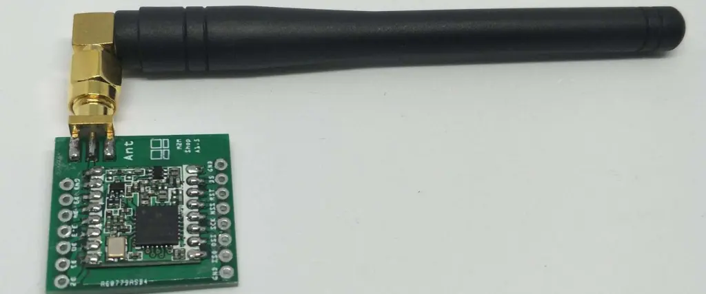
We can do interfacing with any GPS module containing serial communication, but the most popular GPS module is the U-BLOX Neo 6M GPS module. The U-BLOX Neo 6M module only uses four pins: VCC, GND, RX, and TX. Well, this is because the modules send signals over a simple serial RS232 connection, the same protocol used by the Arduino in the writing of the command โ€œSerial.beginโ€. Simply, the module spits iterative NMEA (National Marine Electronics Association) data strings to the TX pin. NMEA is a standard set protocol shared commonly by all GPS.

Connecting the Arduino GPS module setup

In this connection, there is the usage of an input voltage of +5V from the Arduino’s power side and any of the ground pins. If we use any two pins, the setup works superbly. However, there are several ways that one can achieve this connection. In our design, let’s use pin 3 and pin 4.

One connects the Arduino’s pin 3 to the RX GPS Module’s pin and the Arduino’s pin 4 to the TX pin of the GPS Module. The U-BLOX Neo 6M GPS Module consists of a tiny K833 series 3.3V voltage regulator, which becomes its threshold voltage. SoftwareSerial reads raw data from the GPS for creating a new serial connection and then match the default baud rate of the GPS module you’re using. The “native language” of this GPS is gibberish containing all the information possible for a GPS to provideโ€”for example, time, latitude, longitude, etc. However, there has been development of libraries in such a way that they decode and interpret the string characters automatically. An excellent example of such a library is the TinyGPS++ library.

How is the TinyGPS++ library used?

Concerning Arduino, the most advanced GPS library for making references is (Mikal Hart’s TinyGPS++). After installing this library, set the correct baud rate, RX, and TX pins, and you can now continue.

In any case, if you happen to face trouble in getting data out of your module, plug it at 5V and leave it for about a minute. For GPS modules, you can prolong the “cold start” times. However, some modules have a blinking LED indicator to notify the user that it’s ready and sending data. Always consider such before declaring a device as faulty.

Why use the U-BLOX Neo-6M GPS Module?

neo 6m gps arduino

The U-Blox GPS module is cost-effective, making it very popular. Moreover, it has higher performance compared to other GPS modules since it has a ceramic patch antenna, a backup battery that is conveniently integrable with a wide range of microcontrollers, and an onboard memory chip. The two most popular NEO-6M GPS modules are the GY-GPSV3-NEO and the GY-GPS6MV2. These U-Blox NEO-6M GPS modules consist of quite good engines with high sensitivity, making them better for indoor applications. Furthermore, there exists one compatible rechargeable battery for backup known as the MS621FE and EEPROM for the storage of configuration settings. Because of its inbuilt voltage regulator, this module can work perfectly with a DC input lying between 3.3V and 5.0V.

The heart of the GPS Modules is the U-Blox NEO-6M GPS engine. The NEO-6M module consists of a configurable UART interface for general serial communication, but in this case, the baud rate is 9600. The style of this GPS antenna is different since the GPS signal is right-hand circularโ€“polarized (RHCP), which is quite different from the commonly used whip antennas mainly applied for linear polarized signals. Patch antennas, the most widely used antennas, are flat and generally have a metallic and ceramic body usually mounted on a metal base plate.

Positioning

For an intelligent performance of the GPS receiver, the position of mounting the antenna is critical. When in use, the patch antenna should be leaning parallel to the geographic horizon to ensure that it has a full-sky view and a direct line of sight, catching as many detectable satellites as possible.

This type can track up to a maximum of 22 satellites on 50 channels, hence achieving the industry’s maximum level of sensitivity. It consumes only a 45mA supply current, and it has a tracking of -161 dB. Unlike some other GPS modules, it can do up to 5 locations informs a second with 2.5m horizontal position accuracy.

What signal does an Arduino code generate?

GPS satellites convey at least two radio signals with low power. The signal travels through the line of vision, hence traveling through such media as c, glass, and clouds, but some solid media will inhibit the signal’s travel. Barriers include buildings and peaks. However, these modern receivers are better as they are more efficient and can track through buildings.

 Information types contained in a signal of the GPS

  • Pseudorandom code

It is an ID code that identifies the information in transmission by the satelliteโ€”the satellite page of your device shows which satellites are sharing information with you.

  • Ephemeris data

This data is essential in determining the position of a particular satellite and some other information on the time, the satellite’s health, and the current date.

  • Almanac data

It informs the receiver of the GPS on the location of each satellite at any time of any day and the orbital data for that particular satellite and any other satellite thatโ€™s visible within the system.

More about the NEO-6M GPS module

This module type originally had an externally fixed antenna but with no header pins. There is, therefore, a need to 1get it soldered to the other device, say, Arduino, for consistency.

Component information of the NEO-6M GPS module

ยท The NEO-6M GPS module

The central part of this module is the NEO-6M GPS U-Blox chip. This U-Blox six positioning engine can also brag a TTFF (Time-To-First-Fix) which is below one second. An advantage of using this chip is that it provides a unique feature, Power Saving Mode (PSM), allowing an overall power usage reduction by switching the receiverโ€™s parts ON or OFF selectively. This whole story generally decreases the power consumed by this module to 11mA from 45mA, hence reducing the energy consumed by 34mA. All this makes it suitable and more efficient for these applications that are power-sensitive such as the GPS watch.

The essential information pins of the NEO-6M GPS module chip are further broken down to a “0.1” pitch header, which comprises pins required and actively involved in the entire communication process with the microcontroller through UART. The module above works best for a baud rate of between 4800bps and 230400bps, with the default baud being maintained at 9600bps.

ยท Position fixing LED indicator on the chip

This NEO-6M GPS module contains an LED that plays a part in the process of indicating the condition of location fix by blinking at different rates, which are state-dependent.

If the LED is not blinking, this means that it is in the process of searching satellites. On the other hand, if it flashes every second, this is simply interpreted as meaning that they have identified position Fix.

ยท The 3.3Volts LDO Regulator found on the NEO-6M GPS module

The NEO-6M GPS module chip operates on a voltage range of 2.7V-3.6V. The NEO-6M GPS module introduces the MIC5205 extra-low dropout regulator(3V3). The tolerance of its logic pins is 5V, making it easy to interface it with Arduino or some other logic microcontroller rated 5V without including any other converter of a logic level.

ยท Backup Battery and EEPROM of the module

The designing of the module follows the use of an able dual wire serialized EEPROM of the type HK24C32. It is 4 KB and linked with the NEO-6M GPS chip through a 12C. In addition, a button battery thatโ€™s rechargeable is present in the module in which it acts like a capacitor, increasing the general efficiency of the NEO-6M GPS chip. These two features, an EEPROM with a battery, aids in retaining a Battery Backed RAM (BBR). This battery-backed RAM consists of the clock data, module configuration, and data about the latest position (GNSS orbit data). However, this is not intended for the permanent storage of any data.

The battery aids in retaining time and last location, and in the process, TTFF is significantly reduced to 1 second. It hence gives an allowance of faster locks of position. On the other hand, the absence of a battery makes the GPS cold start always, and therefore driving to the GPS lock may take more time. However, on supplying power, the battery automatically charges, and there is maintaining of the data for a maximum of two weeks in the absence of power.

Here is some demonstration of the four pins of the NEO-6M GPS module:

  • GND- stands for ground pin that requires connecting to the Arduinoโ€™s GND pin during interfacing.
  • TXD, which is the (Transmitter pin), actively gets involved in serial communication as a core pin.
  • RDX- This is the receiver pin involved in perceiving signals. In simpler terms, it is helpful in serialized communication.
  • VCC- This supplies power to the module. We can achieve the connection by directly connecting it with the 5Volts pin of the Arduino.

THE ARDUINO UNO

arduino nano gps

In simple terms, Arduino refers to an open electronic platform working on the basis of an easy-to-handle software and hardware. For example, inputs such as a Twitter message, a finger pressing a button, and a light on a sensor are easily read on an Arduino board, which later on turns it into a clear output such as turning on of an LED, activation of a motor, printing something online, etc. Furthermore, it is possible to command the Arduino board by sending instructions to this microcontroller mounted on its board. We can achieve all this using the wiring-based Arduino language of programming and Arduino software, namely the (IDE), which is in the center position on processing.

Arduino Uno Pin Description  

We describe Arduino Uno as a simple microcontroller board typically founded on an Atmega328P 8-bit microcontroller that also consists of the Atmega328P. In addition, other constituents such as serialized communication, voltage regulating crystal oscillator, et cetera, support the microcontroller. This Arduino Uno consists of 14 digital input and output pins(only six become the PWM outputs), one barrel power jack, USB connection, six analog input pins, one ICSP head. Finally, six analog input pins reset button.

These 14 digital input and output pins are alternately used as either the input or the output using pin mode(), digital read(), and digital write() functions comprised within Arduino programming. The basis of operation of each pin is 5V, can withstand or take a maximum current of 40mA, and contains an inbuilt chin-up resistor ranging from 20-50 Kilo Ohms, which are usually detached by default. Furthermore, some pins perform specific roles such as the following:

  • Two serial pins, pin 0 (Rx) & pin 1 (Tx)- the Rx pin and Tx pin are both useful in receiving and transmitting TTL serialized data. To work perfectly, you connect them to the corresponding Atmega328 USB /TTL serialized chip.
  • Two external interrupts pin 2 and pin 3- normally, we configure these pins to activate a lower value interrupt, a change in value, or either a rising edge or dropping edge.
  • PWM pins, namely pin 3, pin 5, pin 6, pin 9, and pin 11- The four individual pins give a PWM output that is 8-bit using the analogwrite() function.

The connection of an Arduino Uno to the GPS Module

These four pins have a unique connection of UBLOX and an Arduino in this order:

  • GND(Ground)—GND(Ground)
  • TX—Digital (D3) pin
  • RX —Digital (D4) pin
  • Vcc—3.3V

The JHD162a LCD

The ground

The ground pin in this LCD module.

2nd pin(Vcc)

The power / LCD module (there is a supply of +5V at this pin)

3rdpin(VEE)

It is the pin involved in contrast adjustment. For example, the terminals of a 10KOhms potentiometer are connected to the +5V and the ground, then linking the sliding pin with the VEE pin to perform this, t. The voltage at this VEE pin describes the contrast. Here, the standard-setting is in the range of 0.4Volts and 0.9Volts.

4thpin(RS)

It stands for the Register select (RS) pin. There are two registers contained in the JHD162A, namely the commands register and the data register. The Logic HIGH of the Register Select pin is essential in selecting a data register, whereas the logic LOW of the Register Select pin selects the commands register. Making the Register Select pin HIGH, then feeding an output into its data lines (DBO to DB7), the input is therefore taken as data, and you display it on the LCD screen. On the other hand, making the Register Select pin LOW then feeding input into its data lines is a command that it should write to an LCD controller, such as positioning the cursor or a purely clean screen or a manuscript.

5thpin(R/W)

It stands for read and write modes, respectively. The pin plays a part in the assortment of the read and write modes. The logic HIGH, in this case, stimulates read mode at this pin, whereas Logic LOW, in this case, stimulates write mode.

6thpin(E)

It is purposely meant for allowing the module of the LCD. Then, a HIGH signal to a LOW signal on the 6th pin enables the module.

7thpin(DBO) to 14thpin(DB7)

These refer to simple data pins through which you can feed commands and also data into the LCD.

15thpin(LED=)

It is the backlight LEDโ€™s anode. When operated at 5V, there must be a resistor of 560-ohm in a series connection with this pin. The voltage source on the Arduino board (3.3V) can power the backlight led in Arduino-based projects.

Pin16(LED-)

It is the cathode of this backlight LED.

Connection of the Arduino Uno with JHD162a LCD

The connection between Arduino and LCD is in the following order:

  • VSS—GND(Ground)
  • VCC—5Volts
  • VEE—10K-Ohms Resistor
  • RS—AO(The analog pin)
  • R/W—ground pin(GND)
  • Connect E to A1
  • Then D to A2
  • Connect D5 to A3
  • Then to D6 to A4
  • Connect D7 to A5
  • Next connect LED+ to VCC
  • Connect LED- to GND(Ground)

Programming of the Arduino

The programming happens with the Arduino IDE. The following is an example of an Arduino program:

#include <LiquidCrystal.h>

// calling the major files and functions

#include <SoftwareSerial.h>

#include <TinyGPS.h>

//long   lat,lon; // create the variable for latitude & longitude object

float lat = 28.5458,lon = 77.1703; // create the variable to represent latitude & longitude object

SoftwareSerial gpsSerial(3,4);//rx,tx

LiquidCrystal lcd(A0,A1,A2,A3,A4,A5);

TinyGPS gps; // create the gps object

void setup(){

Serial.begin(9600); // connect serial

//Serial.println(“The GPS Received Signal:”);

gpsSerial.begin(9600); // connect the gps sensor

lcd.begin(16,2);

}

void loop(){

    while(gpsSerial.available()){ // check for the gps data

    if(gps.encode(gpsSerial.read()))// encode the gps data

    {

    gps.f_get_position(&lat,&lon); // get latitude and longitude

    // display position

    lcd.clear();

    lcd.setCursor(1,0);

    lcd.print(“GPS Signal”);

    //Serial.print(“Position: “);

    //Serial.print(“Latitude:”);

    //Serial.print(lat,6);

    //Serial.print(“;”);

    //Serial.print(“Longitude:”);

    //Serial.println(lon,6);

    lcd.setCursor(1,0);

    lcd.print(“LAT:”);

    lcd.setCursor(5,0);

    lcd.print(lat);

    //Serial.print(lat);

    //Serial.print(” “);

    lcd.setCursor(0,1);

    lcd.print(“,LON:”);

    lcd.setCursor(5,1);

    lcd.print(lon);

   }

  }

  String latitude = String(lat,6);

    String longitude = String(lon,6);

  Serial.println(latitude+”;”+longitude);

  delay(1000);

}

Reading raw data from the GPS through the micro hornet GPS chip

In the interpretation of raw data from the GPS, there is creation of a new serial connection using SoftwareSerial. Then, there is the matching of the default baud rate of the GPS module. For example, the code below simply outputs to the serial monitor whatever it reads from the GPS, excluding any filtering:

#include <SoftwareSerial.h>

Static cosnt int RXpin = 4, TXPin = 3;

Static const uint32_t GPSBaund = 9600;

// The serial connection to the GPS device

SoftwareSerial ss(RXPin, TXPin)

Void loop()

{

Serial begin (115200);

ss.begin(GPSBaund);

}

Void loop()

{

//output raw GPS data to the serial monitor

While (ss.available() > 0) {

Serial.write(ss.read());

}

The serial monitor should then produces a โ€œgibberishโ€ output.

Having gotten the above output, we can now use a library to decode and interpret the output. We can use the tinyGPS++ library in this case.

We can now look at U-Center software and get to know what itโ€™s all about.

U-Center Software

The U-Center software is a vital tool used in the assessment, performance analysis, and the general formation of the u-blox GPS receivers containing the NEO-6M. It’s free software that is only applicable and useable on the windows platform. It can be useful in the display of real-time designed and graphical data visualization from any GPS receiver such as:

  • Navigation summary view
  • Satellite summary view
  • Chart view for any two chosen parameters
  • Clock, altimeter, Speedometer, compass

How to connect NEO-6M to U-center

In this case, the connection of the NEO-6M to PC happens using any USB to TTL converter.

Having installed U-center, you can now start from the general start menu, which is as shown below:

(All programs-> u-Blox->u-center->u-center)

The start menu forms a basis for the location process to commence. You then need to trace the communication toolbar on the screen generated by the start menu and click it. It will then generate a list containing all existing COM ports. Now select the corresponding COM port where the receiver is connected. Raw NMEA sentences are then displayed, which is handy for a quick inspection of the visible ASCII originating from the module over USB. We can use the U-center to show positions on pre-calibrated or Google online maps, often referred to as dynamic maps. When we interface this kind of setup with Arduino, it can be straightforward to generate authentic images showing the actual position of any tracked object at any particular specified time.

The micro hornet GPS Chip

It is the smallest fully integrated GPS antenna module in the world, measuring only 10mm by 10mm by 5.8mm. As a result, it offers an improved receiver combined with higher sensitivity, improved noise immunity, and unconditional frequency stability. Despite its small size, it assimilates a patch antenna element, saw filter, stcxo, rtc crystal, rf shield, Luna, and power management unit with a sirfstariv GPS processor. As a result, it has unique performance and superior sensitivity, achieving a quick time to first fix (TTFF) in less than 1 second, a precision of roughly 1 minute, and a tracking sensitivity of -163dbm.

Conclusion

We are living in an era where Arduino has proven to be the most effective and highly compatible microcontroller supporting the creation of programmable interactive electronic objects. It works based on input and direct output, displaying the entire output in an LCD. In the above article, we’ve studied the relationship between Arduino and various GPS modules, for example, the NEO-6M-GPS module. We’ve also learned different versions of the Arduino, such as the Arduino Uno, their basic structure, and more on their interaction with these GPS modules. Finally, we’ve also seen the micro hornet GPS chip, which is very efficient and modest and a good chip to consider for academic projects. Hence if you are looking to work on a GPS Arduino project, then we would say that “you have got all you need to start your project,” all the best.