
RAYPCB · ENGINEERING REFERENCE
Mini LED PCB: plan the array before releasing the panel
Connect LED package pitch, board geometry, driver organization and thermal requirements. Explore a rectangular array and prepare a controlled assembly handoff.
Original engineering guidance · References checked September 28, 2026
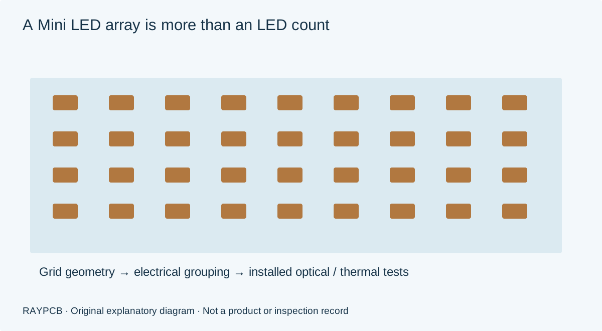
Mini LED PCB design connects an array to a manufacturing process
A Mini LED PCB supports a dense LED array and its electrical, thermal and assembly interfaces. It can serve a display backlight or another compact lighting arrangement. The useful design question is not only how small an LED is: the board must place the selected package consistently, route its connections, distribute power, support heat flow and meet the optical system's mechanical requirements.
Mini LED terminology does not define a universal package size, pitch or manufacturing capability. Use the exact LED drawing, land pattern and product architecture. A backlight organized into dimming zones also needs a defined relationship between LEDs, strings, channels and zones. One LED is not automatically one independently controlled zone.
This page focuses on array geometry and the manufacturing handoff. For general substrate choices and lighting-board thermal comparisons, see LED PCB materials and design. Keep optical requirements, driver behavior and board production requirements connected, but do not expect a geometry calculator to determine brightness uniformity or junction temperature.
Define the array at three different levels
| Level | Definition to freeze | Common ambiguity |
|---|---|---|
| Package and land pattern | Exact LED variant, polarity, dimensions and approved footprint | Package body confused with the full placement reservation |
| Electrical organization | Series count, channel mapping, current and dimming behavior | LED count treated as driver-channel or zone count |
| Optical and mechanical system | Board datum, pitch, optical gap and mounting | Uniform pitch assumed to guarantee uniform illumination |
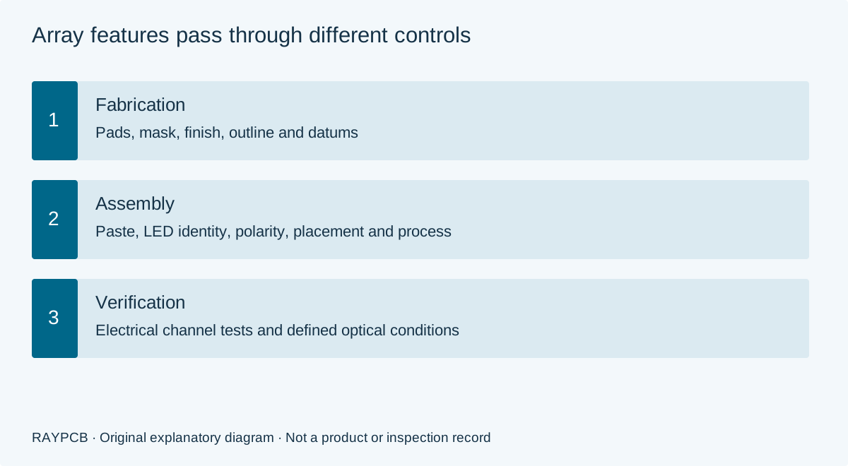
Start by agreeing which of these requirements the PCB supplier is expected to implement. The board fabricator needs copper, mask, outline and finish definitions. The assembler needs the LED identity, orientation, placement tolerances and process requirements. The system team owns the optical targets and the conditions under which they will be evaluated.
Driver architecture influences the route from a visible array to electrical channels. For example, TI's TLC69601-Q1 product information describes a multi-channel device for local-dimming backlights. It is a reference for the selected device's capabilities, not a recommendation for every array or evidence that a board has passed a lighting requirement.
Explore a rectangular array and its electrical load
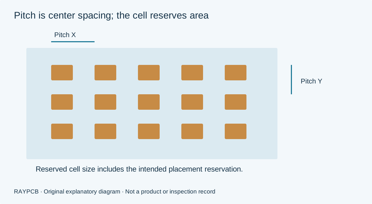
Enter the board width and height, an edge margin, the reserved cell width and height, and center-to-center pitch in both directions. The cell reservation should include the space you intend to protect around each placement, not just an LED body outline. The calculation uses a regular rectangular grid with no mounting holes, connector exclusions, staggered rows or routing obstacles.
RAYPCB ENGINEERING
Industry EngineeringMini LED PCB worksheet
Loading Mini LED PCB worksheet…
The count on each axis is floor((board dimension − two margins − reserved cell size) / pitch) + 1 when a cell fits. Otherwise it is zero. The example uses a 100 × 60 mm board, 5 mm margins, 2 × 2 mm reserved cells and 6 mm pitch. It fits 15 × 9 cells, or 135 LEDs, before any additional keepouts are considered.
With an illustrative 3 V forward drop, 10 mA on-current and 50% duty, the arithmetic average LED electrical load is 2.025 W. This assumes identical LEDs and the entered duty for every LED. It excludes driver and distribution losses, dynamic waveforms, optical output and thermal resistance. A dimming pattern with different channel activity needs a more detailed load model.
Choose a substrate for routing, assembly and heat flow
Substrate choice should follow the electrical organization, power density, mechanical envelope and manufacturing route. An FR-4 multilayer construction can support more complex routing and driver placement. A metal-core construction can provide a different path for heat, but its dielectric, isolation and routing limitations still need review. The correct comparison is between defined constructions, not just material names.
For a metal-base option, compare the dielectric thickness, thermal conductivity basis, copper and base material with the required insulation and mechanical conditions. Visit the metal core PCB guide for that construction discussion. Do not infer the temperature of an LED junction from the conductivity of a single material layer or assume a metal base eliminates interface resistance.
For multilayer FR-4, consider copper distribution, the driver side, local heat sources and attachment to the enclosure or heat spreader. Preserve the mounting and interface requirements when moving from a sample board to a panelized build. Mechanical flatness and optical alignment requirements should be stated explicitly rather than implied by a photograph of an illuminated board.
Control pads, mask, polarity and panel identity
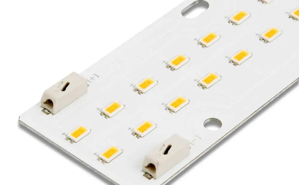
Use the LED manufacturer's land pattern as the starting point and review it against the intended assembly process. Distinguish the copper land, solder-mask opening and paste aperture. They are related geometries with different purposes. Blanket enlargement or reduction can change solder volume, alignment behavior and the risk of bridging; agree the actual package and process before setting them.
Dense repeated patterns make a small systematic error expensive. Confirm polarity conventions between the schematic symbol, package drawing, placement file and inspection reference. Include unambiguous board and panel datums so repeated units cannot be confused by orientation or mirroring. A silkscreen arrow may be useful, but it should not be the only source of placement truth.
Discuss the panel with the assembler. Support during printing and placement, edge handling, fiducials, separation and optical-surface protection can all matter. The assembly panelization guide provides the broader preparation route. Keep mounting and optical keepouts visible on the drawing, especially where automated array generation makes the copper pattern look deceptively regular.
Connect manufacturing stages to the array's critical features
First, review the released artwork, outline, material and the assembly reservation around each LED. Next, fabricate and inspect the defined pad and mask features. Assembly then adds paste deposition, component placement and the agreed thermal process. Finally, electrical and optical checks evaluate the populated configuration under stated operating conditions. Each stage needs its own inputs and evidence.
Solder-paste printing deserves attention because repeated small deposits can amplify process variation across a large array. Define the stencil from the actual package and process requirements, not from an arbitrary pitch category. Use the PCB stencil design guide to prepare aperture and thickness questions. Inspection of paste deposits, where included in the process plan, answers a different question from inspection after reflow.
After assembly, specify how missing, reversed, open or shorted LEDs are detected and how channels are exercised. If appearance matters, identify the optical setup, stabilization time, ambient conditions and measurement method. Do not use a camera image with automatic exposure as a substitute for an agreed quantitative optical test.
Keep electrical input, emitted light and heat distinct
The array tool reports electrical input to the LEDs under simplified assumptions. Some input becomes emitted optical energy and the rest contributes to heat, while drivers and conductors add their own losses. The electrical total is therefore not a junction-temperature result. Thermal analysis needs the actual package, board path, interfaces, enclosure and operating pattern.
For local dimming, the most relevant thermal pattern may differ from a uniform full-array image. Consider sustained operating states and nearby driver heating, then select representative validation conditions. Keep the LED current and duty definitions clear: a peak on-current and a time-averaged current cannot be substituted without considering the waveform and device limitations.
Measure the installed configuration with an appropriate method and retain the LED and board revisions. If an interface pad, adhesive or mounting pressure changes, review whether previous thermal evidence remains representative. A good manufacturing drawing preserves the interfaces needed by the thermal design instead of leaving them to assembly improvisation.
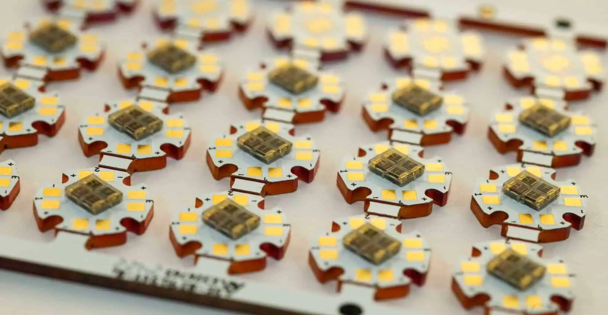
Example: pitch changes both count and the review scope
Using the worksheet's 100 × 60 mm example, changing both pitches from 6 mm to 5 mm gives 18 columns and 10 rows under the same margins and cell reservations. The idealized count increases from 135 to 180 LEDs. At the same illustrative voltage, current and duty, the arithmetic electrical load rises from 2.025 W to 2.7 W.
That count increase does not prove that the revised array can be routed, assembled or cooled. Check channel organization, connectors, copper distribution and the optical arrangement. A mounting hole or reserved driver region can remove positions that the rectangular model currently counts. If the reserved cell size approaches pitch, confirm that the reservation includes the intended manufacturing clearance rather than just the package body.
This is an original planning scenario, not a tested Mini LED product. Its purpose is to expose the consequences of a geometric decision early. Use the saved inputs to discuss the design with the relevant teams, then replace the idealized count with the released layout before a purchase order is finalized.
What drives Mini LED PCB and assembly cost?
Board area, layer construction, material, finish, pad and mask definition, panel utilization and required inspection affect fabrication cost. Assembly adds the exact LED package, placement quantity, stencil preparation, handling, yield-related process work and test scope. A higher LED count can affect assembly time and test requirements even when the board dimensions remain unchanged.
Separate prototype setup from recurring production. Ask whether programming, optical fixtures, electrical fixtures and characterization work are included, excluded or quoted separately. Component supply and binning requirements can also change procurement assumptions. A simple cost per square centimeter cannot capture all these differences or establish a current market price.
For a useful enquiry, send the board files and drawing, exact LED and driver part numbers, populated variant, quantity, intended operating pattern and optical or thermal requirements. Mark unresolved requirements clearly. Use PCB Manufacturing for the bare board and PCB Assembly for component placement and the agreed test scope. The worksheet is optional; it is not a mandatory step before contacting the team.
Mini LED PCB questions
Is every LED in the array a separate dimming zone?
No. Zone organization depends on the electrical architecture and driver mapping. The geometric worksheet counts LED positions only and does not infer strings, channels, zones or the available driver outputs.
Does a white board surface guarantee optical performance?
No. Surface appearance is one aspect of an optical system. Material, finish, geometry, optical layers, operating conditions and aging requirements need their own definitions and evidence. A photograph cannot establish reflectance or illumination uniformity.
Can the tool generate a production-ready layout?
No. It estimates a regular rectangular array and a simplified electrical load. The actual CAD layout must include pads, routing, holes, fiducials, keepouts and the approved manufacturing rules before fabrication or assembly review.
Bring a focused question with the design revision
Send the board revision, construction, quantity and the layout, file or manufacturing question you need reviewed. Identify unresolved requirements so the response can address them.
Send requirements for reviewOptional: attach the downloaded worksheet manually. Use the worksheet as a discussion record; manufacturing requirements and verification must be agreed for the actual project.