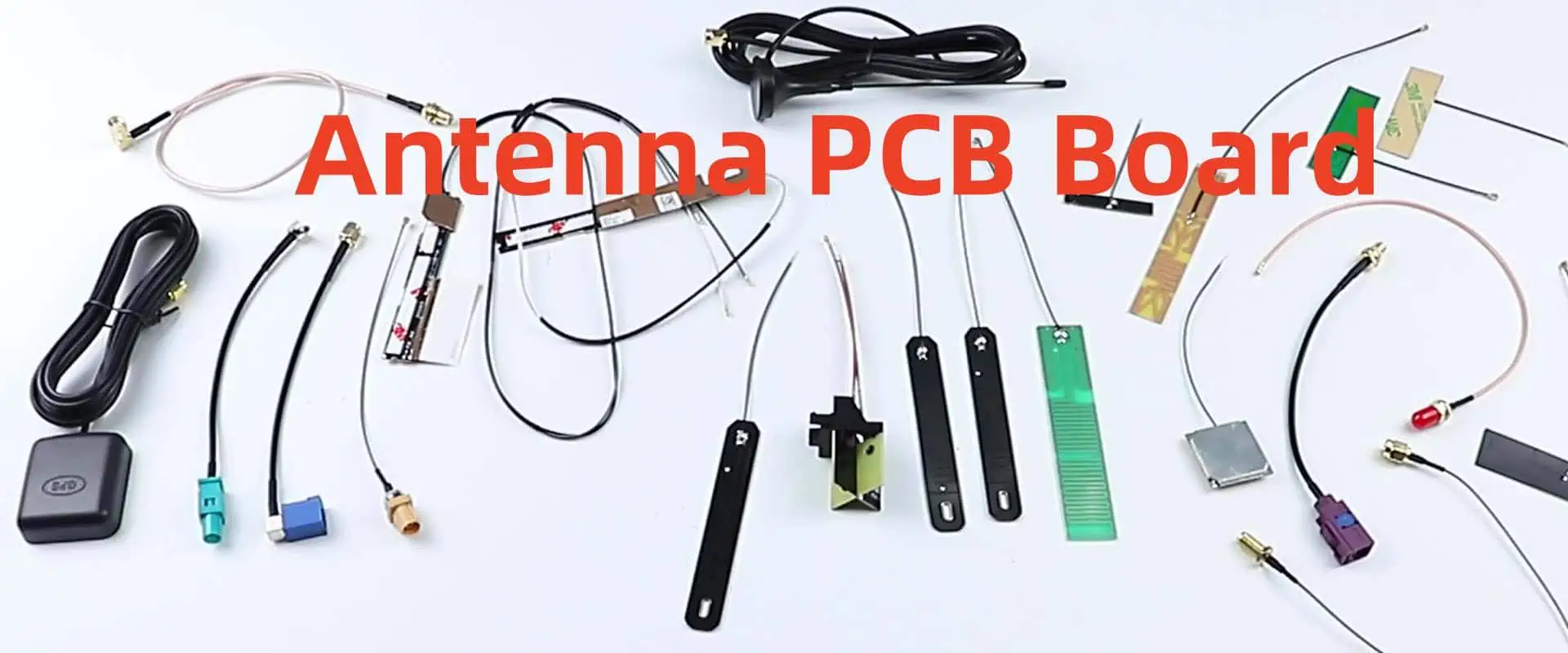
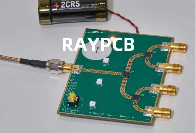
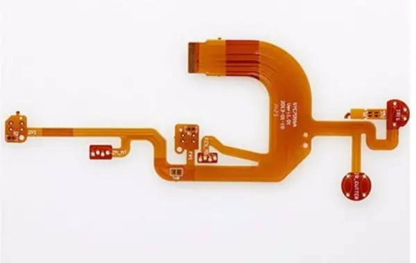
A wide variety of antennas are available as off-the-shelf components, making them a convenient choice for engineers designing systems that require wireless communication. However, antennas used in PCBs can also be printed directly onto the board, enabling fully customized designs and unique architectures that integrate seamlessly into a single assembly. Additionally, PCB-mounted antennas, such as chip antennas or System-on-Chip (SoC) modules with integrated radios, may require either an antenna module or an off-the-shelf component to function effectively.
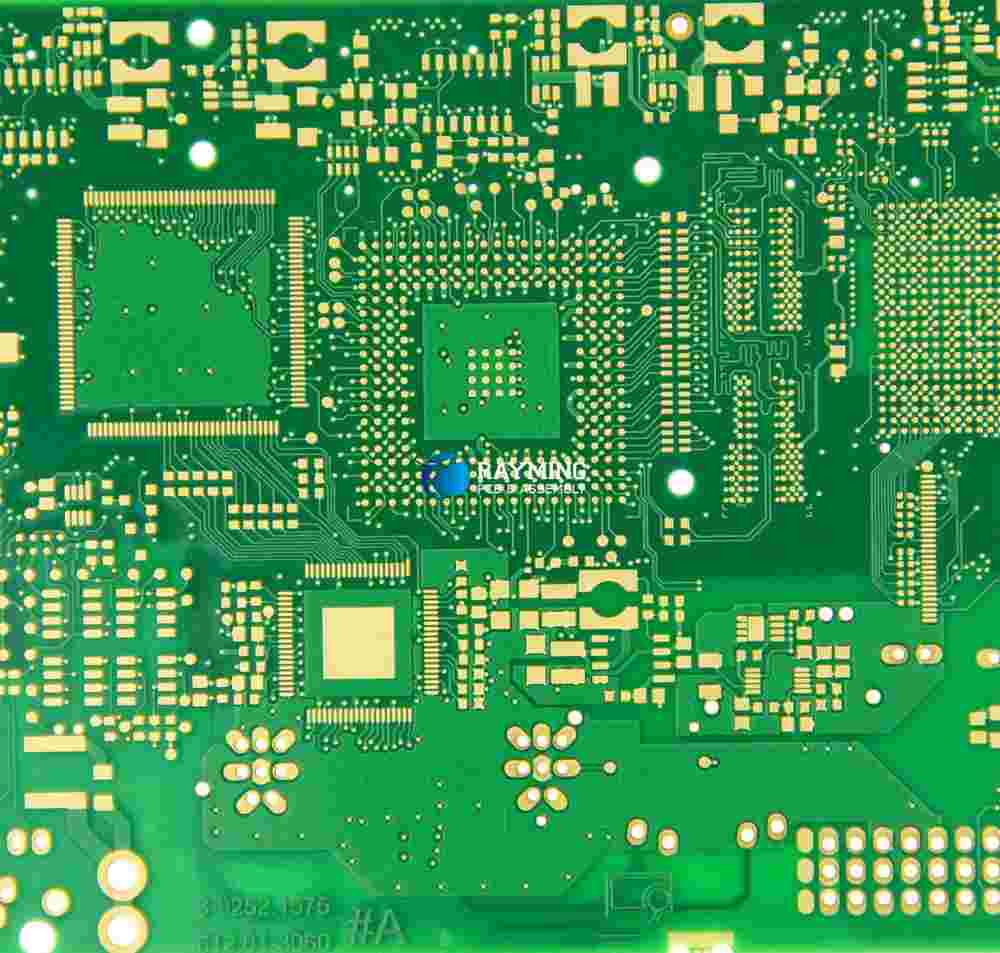
Whether the antenna is printed directly onto the PCB or sourced as a pre-made component, it is crucial for PCB designers to have a deep understanding of how antennas operate. Experienced designers will recognize that a PCB itself contains numerous elements that can unintentionally act as efficient antennas. In this article, we will explore some of the fundamental concepts behind antennas, providing engineers with the knowledge needed to design, select, and position antennas effectively in their projects.
What is PCB Antenna?
A PCB antenna, short for Printed Circuit Board antenna, is a type of antenna fabricated directly onto a printed circuit board. Unlike traditional antennas that are separate components, PCB antennas are integrated into the circuit board itself, making them an integral part of the device’s overall design.
PCB antennas offer several advantages:
- Cost-effective: They eliminate the need for separate antenna components, reducing overall production costs.
- Space-saving: PCB antennas are ideal for compact devices where space is at a premium.
- Consistency: Being part of the PCB ensures consistent performance across manufactured units.
- Durability: Integrated into the board, these antennas are less prone to damage from external factors.
Patch
| Band / Standard | Frequency Range | Wavelength | Type | Applications |
|---|---|---|---|---|
| GPS L1 | 1575.42 MHz | 190.3 mm | GPS | Navigation, Timing |
| GPS L2 | 1227.60 MHz | 244.3 mm | GPS | Precision Navigation |
| GPS L5 | 1176.45 MHz | 254.8 mm | GPS | Safety-of-Life |
| WiFi 2.4 GHz | 2.400 - 2.4835 GHz | 124.9 mm | WiFi | 802.11b/g/n/ax |
| WiFi 5 GHz | 5.150 - 5.850 GHz | 58.3 mm | WiFi | 802.11a/n/ac/ax |
| WiFi 6E / 7 | 5.925 - 7.125 GHz | 50.6 mm | WiFi | 802.11ax/be |
| Bluetooth | 2.402 - 2.480 GHz | 124.8 mm | IoT | BLE, Classic BT |
| LoRa 868 | 863 - 870 MHz | 347 mm | IoT | LPWAN Europe |
| LoRa 915 | 902 - 928 MHz | 328 mm | IoT | LPWAN Americas |
| LTE Band 7 | 2500 - 2690 MHz | 120 mm | Cellular | 4G LTE |
| 5G n78 | 3.3 - 3.8 GHz | 90.9 mm | Cellular | 5G Sub-6 GHz |
| 5G mmWave n260 | 37 - 40 GHz | 8.1 mm | Cellular | 5G mmWave |
| Zigbee | 2.400 - 2.4835 GHz | 124.9 mm | IoT | Home Automation |
| Thread/Matter | 2.400 - 2.4835 GHz | 124.9 mm | IoT | Smart Home |
| UWB | 6.0 - 8.5 GHz | 50 mm | IoT | Ranging, Location |
| NFC | 13.56 MHz | 22.1 m | IoT | Contactless |
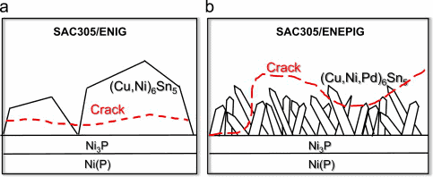
| Finish | RF Suitability | Shelf Life | Cost |
|---|---|---|---|
| ENIG | Excellent | 12+ months | $$$ |
| OSP | Very Good | 6 months | $ |
| Immersion Tin | Good | 6 months | $$ |
| HASL | Poor | 12 months | $ |
| Immersion Silver | Excellent | 6 months | $$ |
| Parameter | Standard | RF Grade |
|---|---|---|
| Trace Width | ±20% | ±10% |
| Dielectric Thickness | ±10% | ±5% |
| Impedance | ±15% | ±5% |
| Registration | ±100 μm | ±50 μm |
| Copper Thickness | ±20% | ±10% |
Learn more about:
How PCB Antenna Works
PCB antennas function based on the same principles as traditional antennas. They are designed to transmit and receive electromagnetic waves at specific frequencies. The key difference lies in their construction and integration with the circuit board.
Here’s a brief overview of how PCB antennas work:
- Signal Generation: The device’s circuitry generates an electrical signal.
- Conversion: The antenna converts this electrical signal into electromagnetic waves for transmission.
- Radiation: The electromagnetic waves are radiated into the surrounding space.
- Reception: For incoming signals, the process is reversed. The antenna captures electromagnetic waves and converts them back into electrical signals.
The specific design of the PCB antenna, including its shape, size, and placement on the board, determines its frequency range, radiation pattern, and overall performance.
Types of PCB Antennas

There are various types of PCB antennas, each with its unique characteristics and applications. Let’s explore some of the most common types:
1. PCB Monopole Antenna
The PCB monopole antenna is one of the simplest and most widely used designs. It consists of a single conductive element, typically a straight trace on the PCB, with a ground plane.
Key features:
- Simple design
- Omnidirectional radiation pattern
- Suitable for a wide range of frequencies
- Commonly used in mobile devices and IoT applications
2. PCB Dipole Antenna
A PCB dipole antenna consists of two identical conductive elements, often arranged in a straight line. Unlike the monopole, it doesn’t require a ground plane.
Key features:
- Balanced design
- Bi-directional radiation pattern
- Good performance in free space
- Used in RFID tags and wireless sensors
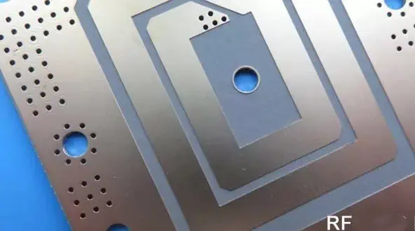
3. PCB Patch Antenna
Also known as a microstrip antenna, the PCB patch antenna consists of a flat rectangular sheet or “patch” of metal on top of a larger sheet of metal (ground plane) separated by a dielectric substrate.
Key features:
- Low profile and lightweight
- Directional radiation pattern
- High gain
- Commonly used in GPS receivers and satellite communications
4. PCB Loop Antenna

PCB loop antennas are formed by creating a loop of conductive material on the PCB. They can be circular, square, or other shapes.
Key features:
- Compact size
- Good performance in near-field applications
- Often used in NFC and RFID systems
- Suitable for low-frequency applications
5. PCB Helical Antenna
A PCB helical antenna is created by forming a helical pattern on the PCB. It’s essentially a three-dimensional structure created on a two-dimensional surface.
Key features:
- Circular polarization
- High gain
- Narrow beamwidth
- Used in satellite communications and GPS applications
6. PCB Slot Antenna
PCB slot antennas are created by cutting a slot in the ground plane of the PCB. The slot acts as the radiating element.
Key features:
- Low profile
- Can be integrated into existing ground planes
- Bidirectional radiation pattern
- Used in mobile devices and aircraft communications
7. PCB Yagi Antenna
A PCB Yagi antenna, also known as a Yagi-Uda antenna, consists of multiple elements including a driven element, reflector, and one or more directors.
Key features:
- High directivity
- High gain
- Used for point-to-point communications
- Common in TV antennas and long-range Wi-Fi
8. Planar Inverted F Antenna (PIFA)
The PIFA is a variation of the monopole antenna, with the top section folded down to be parallel with the ground plane.
Key features:
- Compact size
- Good performance close to the human body
- Widely used in mobile phones
- Can be easily integrated into handheld devices
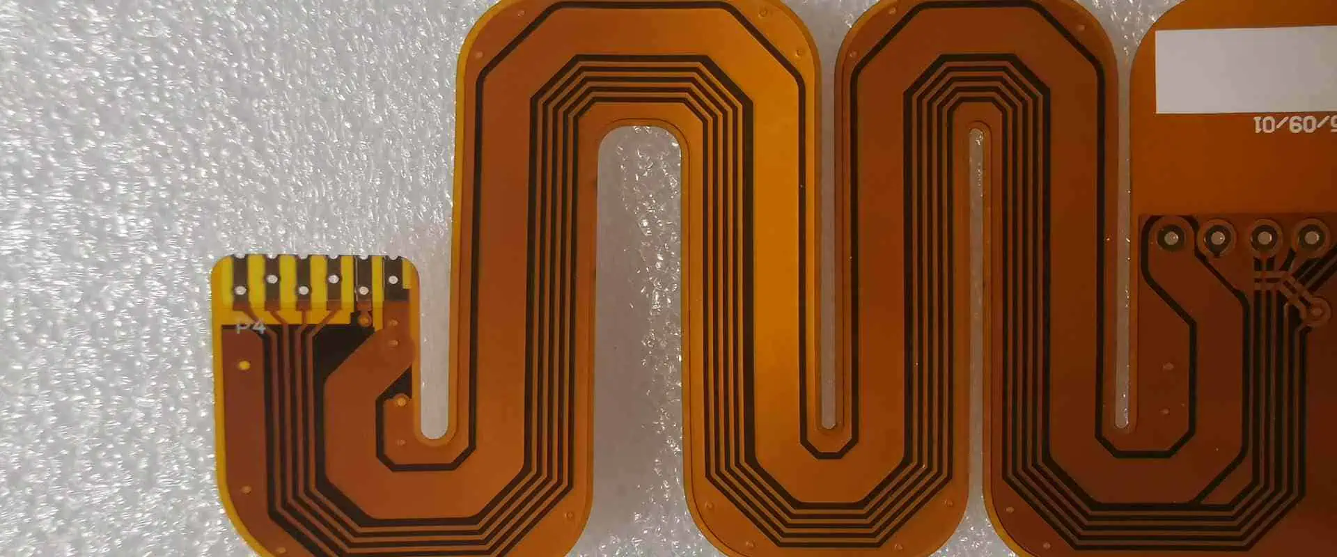
9. Meander Line Antenna
A meander line antenna is created by forming a meandering pattern on the PCB, effectively increasing the electrical length of the antenna while maintaining a compact physical size.
Key features:
- Very compact design
- Suitable for low-frequency applications in small devices
- Used in wearable technology and IoT devices
- Can be tuned by adjusting the meander pattern
10. NFC Antenna PCB
NFC (Near Field Communication) antennas are specialized loop antennas designed for short-range communication.
Key features:
- Very short range (typically a few centimeters)
- Low power consumption
- Used in contactless payment systems and access control
- Often integrated into smartphones and smart cards
11. LoRa Antenna PCB

LoRa (Long Range) antennas are designed for long-range, low-power communication in IoT applications.
Key features:
- Long-range capability (up to several kilometers)
- Low power consumption
- Used in smart city applications, agriculture, and industrial IoT
- Often implemented as monopole or dipole antennas
12. LTE Antenna PCB
LTE (Long-Term Evolution) antennas are designed for high-speed mobile communication.
Key features:
- Broadband performance to cover multiple LTE bands
- Often implemented as MIMO (Multiple-Input Multiple-Output) systems
- Used in smartphones, tablets, and mobile hotspots
- May be designed as patch, PIFA, or other antenna types
13. Wi-Fi PCB Antenna
Wi-Fi PCB antennas are designed to operate in the 2.4 GHz and 5 GHz bands used by Wi-Fi networks.
Key features:
- Dual-band operation (2.4 GHz and 5 GHz)
- Often implemented as patch or inverted-F antennas
- Used in routers, laptops, and IoT devices
- May incorporate MIMO technology for improved performance
14. 2.4 GHz PCB Antenna
2.4 GHz antennas are designed specifically for the popular 2.4 GHz ISM (Industrial, Scientific, and Medical) band.
Key features:
- Compact size due to high frequency
- Used in Wi-Fi, Bluetooth, and ZigBee applications
- Often implemented as monopole or inverted-F antennas
- Wide variety of designs available due to the popularity of the band
15. PCB Trace Antenna
PCB trace antennas are formed by carefully designed traces on the PCB itself, without additional components.
Key features:
- Very low cost
- Integrated directly into the PCB design
- Can be implemented in various shapes (meandered, spiral, etc.)
- Used in low-cost devices and RFID tags
What are the Best Materials for Circuits with Antennas?
Choosing the right materials for PCB antennas is crucial for optimal performance. The key factors to consider are the dielectric constant (εr) and the loss tangent of the substrate material. Here are some commonly used materials:
-
FR-4: A popular and cost-effective choice for many applications. It has a dielectric constant of about 4.4 and is suitable for frequencies up to about 1 GHz.
-
Rogers RO4350B: This material offers lower loss and better performance at high frequencies compared to FR-4. It’s often used for antennas operating above 1 GHz.
-
Taconic RF-35: Another high-performance material with low loss, suitable for high-frequency applications.
-
PTFE (Teflon): PTFE-based materials offer very low loss and are excellent for high-frequency and high-performance applications. However, they are more expensive and harder to process.
-
Ceramic-filled PTFE composites: These materials offer a good balance between performance and processability.
The choice of material depends on the specific requirements of the antenna, including frequency range, performance needs, and cost constraints.
Choosing an Antenna
Selecting the right antenna for your application involves considering several factors:
-
Frequency Range: The antenna must be designed for the specific frequency or range of frequencies required by your application.
-
Size Constraints: The available space in your device will influence the type and size of antenna you can use.
-
Radiation Pattern: Different applications require different radiation patterns. For example, a mobile phone might need an omnidirectional pattern, while a satellite dish needs a highly directional pattern.
-
Gain and Efficiency: Higher gain antennas can transmit and receive signals over longer distances but may have more directional radiation patterns.
-
Environmental Factors: Consider the environment in which the antenna will operate, including proximity to other components, potential interference sources, and physical conditions.
-
Cost: Some antenna designs are more complex and expensive to manufacture than others.
-
Regulatory Compliance: Ensure that your chosen antenna meets all relevant regulatory requirements for your target markets.
Antenna Design Principles for PCB Designers

Designing effective PCB antennas requires a good understanding of RF principles and careful consideration of various factors. Here are some key principles to keep in mind:
-
Impedance Matching: The antenna should be matched to the impedance of the feed line (typically 50 ohms) to maximize power transfer and minimize reflections.
-
Ground Plane Considerations: Many PCB antennas require a ground plane. The size and shape of this ground plane can significantly affect antenna performance.
-
Trace Width and Spacing: The width of PCB traces and their spacing from other traces and ground planes can affect the antenna’s characteristics.
-
Antenna Placement: The location of the antenna on the PCB can impact its performance. Keep it away from noise sources and consider the effects of nearby components.
-
Use of Vias: Vias can be used to create connections between layers and to implement certain antenna designs, but their placement must be carefully considered.
-
Simulation and Modeling: Use electromagnetic simulation tools to model and optimize your antenna design before fabrication.
-
Prototyping and Testing: Always prototype and test your antenna designs to verify their performance in real-world conditions.
Performance Testing and Optimization
Once a PCB antenna is designed and fabricated, it’s crucial to test its performance and optimize it if necessary. Here are some key aspects of antenna testing and optimization:
-
S-Parameter Measurements: Use a vector network analyzer to measure S-parameters, particularly S11 (return loss), which indicates how well the antenna is matched to its feed line.
-
VSWR Measurement: The Voltage Standing Wave Ratio is another measure of impedance matching.
-
Radiation Pattern Measurement: This shows how the antenna radiates energy in different directions.
-
Gain Measurement: Determine the antenna’s gain, which indicates how well it concentrates energy in a particular direction.
-
Efficiency Measurement: This indicates how much of the input power is actually radiated by the antenna.
-
Bandwidth Measurement: Verify that the antenna performs well across its intended frequency range.
-
Near-Field Scanning: This can help identify areas of high field strength on the PCB, which can be useful for EMC considerations.
After testing, optimization might involve:
- Adjusting the antenna’s dimensions
- Modifying the matching network
- Changing the antenna’s position on the board
- Altering the ground plane design
- Using different PCB materials
Iterative testing and optimization are often necessary to achieve the best possible performance.
PCB Antenna vs. Chip Antenna
When designing an RF system, engineers often need to choose between PCB antennas and chip antennas. Here’s a comparison of the two:
PCB Antenna
Advantages:
- Lower cost, especially in high volumes
- Can be customized for specific applications
- No additional components required
- Can achieve better performance in some cases
Disadvantages:
- Requires more PCB space
- Performance can be affected by other components and PCB layout
- May require more design and optimization time
Chip Antenna
Advantages:
- Very compact size
- Consistent performance across different devices
- Easier to implement, especially for inexperienced designers
- Less affected by nearby components
Disadvantages:
- Higher component cost
- Limited customization options
- May have lower performance compared to well-designed PCB antennas
- Requires a specific ground plane size for optimal performance
The choice between PCB and chip antennas depends on factors such as available space, design expertise, production volume, and performance requirements. In many cases, PCB antennas offer a good balance of cost, performance, and flexibility, making them a popular choice for many applications.
Conclusion
Antenna PCB technology has revolutionized the world of wireless communication, enabling the creation of compact, efficient, and cost-effective devices. From simple monopole designs to complex MIMO systems, PCB antennas offer a wide range of solutions for various applications.
As an RF engineer, understanding the principles of PCB antenna design, the characteristics of different antenna types, and the factors that influence antenna performance is crucial. By carefully considering these aspects and following best practices in design, testing, and optimization, you can create PCB antennas that meet the demanding requirements of modern wireless systems.
As technology continues to evolve, PCB antennas will undoubtedly play an increasingly important role in shaping the future of wireless communication. Whether you’re working on IoT devices, mobile phones, satellite systems, or any other wireless application, mastering the art and science of PCB antenna design will be a valuable skill in your RF engineering toolkit.


