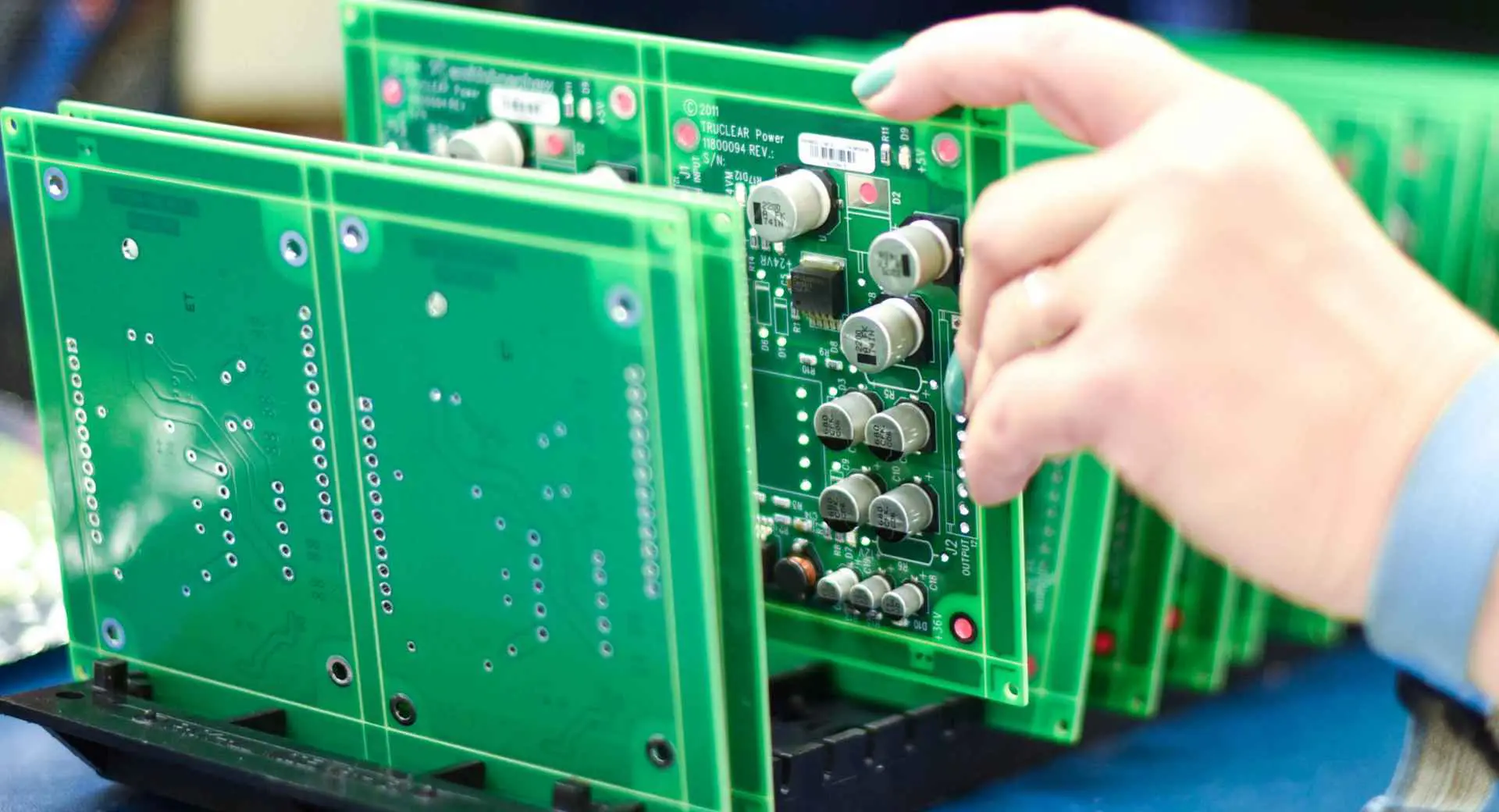
The global competition in the field of manufacturing technology is increasing day by day. Engineers are finding ways to come up with the solution that can greatly decrease the cost of their product while maintaining or enhancing quality. In the domain of electronic and electrical engineering, Printed Circuit Boards (PCBs) are the core of hardware engineering and their cost greatly affects the overall cost of the product. Hence it is crucial that one find the cheap PCB assembler and PCB fabrication vendor that will provide good quality in reasonable price.
However it is observed that many suppliers providing cheap prototype PCB assembly will lower the quality and thus the user will suffer in terms of failure and noncompliance. There are different PCB assemblers providing different quotations to their customers, hence one should through check the portfolio and services along with terms and condition to save money cut down the PCB assembly cost. Hence the user must keep a good balance between cost and quality of PCB assembly. It is therefore necessary that customer must know it budget constraints and find assembler accordingly while in parallel optimize the circuit design or PCB layout at design stage so as to cut PCB assembly cost.
Now we will discuss some major techniques that can be used to cut PCB assembly cost while maintaining good quality.
1. Locate a reliable, professional, and “low-cost” PCB assembler.
Many PCB assemblers claim cost effective solution and services but they do not provide as they state. Hence first of all you should know completely about your project requirements and limits of your budget, then after this go for the detailed examination of a particular assembler / supplier. This will require effort in searching internet, visiting websites, reading blogs and checking comments and reviews of user but all this will help you in long run by locating a perfect assembler that meets your project requirements and budget constraints. You can then keep good ties with that assembler so that in more projects you can get more discount on your PCB assembly. While searching for PCB assembler you must keep following points in mind
Certificates:
A supplier or PCB assembler having certified documents showing his capability and capacity to meet your specific requirement is always reliable. Certifications like RoHS (Restrictions of Hazardous Substance) and ISO9001 (A international standard for QM) will always be useful in selection of PCB assembler. These certificates ensures that quality provided is up-to mark and that six hazardous materials are not used in the manufacturing of products and fabrication of PCBs.
Equipment:
While planning to choose the right PCB assembler, the equipment plays a very important role. The equipment like SMT components pick and placerobots, high speed and accuracy will greatly increase the quality of PCB.
Component procurement:
At Rayming PCB, we deal lots of customers and we come to know that, time and money are the key points that every customers wants to save. This can be achieved by carefully selecting the PCB assembler that provides “Components Sourcing” services. Many times the customers do not communicate correctly with PCB assemblers which results in unexpected errors in components/parts selection. Hence if you want ensure good quality PCB in reduced cost, you have to find a PCB assembler that has links in local or foreign markets to procure cheap and good components and assemble them on PCB. In this way you will have time to concentrate on your project design.
Moreover, there are also other factors that can also help you to filter out PCB assemblers that do not fit the requirements. Some of these factors are lead time, MOQ (Minimum Order Quantity), shipping methods and obviously quotations and rates.
Just to mention a key point is the “labor”. Like in China, labor is not much expensive like in European countries and in US. So you can choose PCB assembler from China to greatly become cost effective while on the other hand parts cost are mainly dependent on US dollar rate. A slight fluctuation will not pose great effect in overall cost of PCB assembly.
2. Adjust the bare PCB layout design to cut cost
There are many parameters in PCB layout design that can be set by the user end to minimize PCB cost. These parameters are tested by the process name “Design for Manufacturability” DFM check. There are some PCB assemblers that provide this feature free of cost. You can choose that assembler to cut PCB cost.
Now we will discuss some of these parameters that can directly affect the cost of bare PCB. These are:
Number of Layers:
The higher the number of layers the higher the cost of PCB. It is that simple.
Number of Vias:
The higher the number of vias and smaller the diameter of via, the higher the cost of PCB will become. So while designing your PCB layout, carefully place each via either it is buried, blind or micro so that greater functionality of PCB can be obtained with minimum vias.
PCB Dimensions:
The smaller PCBs do not necessarily mean lower cost of PCB. Instead smaller PCBs are complex in nature and contains multiple layers that can increase cost. Hence a designer must carefully design PCB layout so as to keep balance in number of layers and PCB size. In case of SMT PCB size should be such that the PCB will fit exactly on pick and place machines of PCB assembler. The designer should have beforehand knowledge of its PCB assembler capability and constraints.
The shape of PCB can affect the PCB assembly cost. Usually the square or rectangular shape PCBs tend to be less expensive as compared to other special shape PCBs.
Surface Finish:
The quality of PCB is directly proportional to the electrical performance and ability of PCB to accept solder. Hence various types of finishing methods are used at PCB surface that include ENIG, OSP and HASL. This will restrict the solder pads from oxidization and increase quality. Choose the surface finish option that best fits your requirements.
These above discussed tips are based on our extensive experience in the domain of PCB fabrications and assembly. These points must be considered before selecting the right PCB assembler to cut cost and ensure quality.
3. Generate a Perfect BOM.
The very important thing while designing PCB layout is the generation of Bill of Material called (BOM). Many of us take it very lightly. But this BOM things is more important than Gerber generation.
The BOM is a file that a designer generates. The BOM files contains all the information necessary for the PCB assembler to procure components/materials and start PCB assembly process. An incomplete BOM can result in delays and improper components procurement that will result in time and money wastage. Usually the BOM must include, supplier name, manufacturer name, part number, quantity, reference designator, details of parts and package footprint details.
There are PCB assemblers that have their own form for BOM generation. If the designer fills that form and give to the assembler, than it will be helpful for assembler to understand and speedup the assembly process. It is also very important that the design engineer, must keep the “components replacement” in mind. And mention that replacement part number in the BOM. Many times when designing circuit, a particular IC package is discontinued and not further available in market, so giving a replacement option will help the assembler to avoid wastage of time finding the obsolete item.
4. Choose PCB Assembler having links with Components Wholesaler.
The cost of PCBA is directly and obviously proportional to the cost of components. As discussed above in paragraph “Component Procurement”, the customer/designer/user can rely on the PCB Assembler to procure electronic components that are cheap and readily available off the shelf. These PCB assemblers have links and PR to electronic components wholesalers, retailers and distributors and they can arrange very inexpensive components in large quantity like MOQ of 5,000 or 10,000 pieces. In such large amount some pieces can be counterfeit parts which can be ignored.
5. Adjust order quantity.
Another important aspect of cutting the cost of PCBA is the larger volume order. It is a common practice that when you order anything in large amount the cost per unit is low and when you order less the cost per unit will be high. The same is the case for electronic components like resistors, capacitors and ICs and same goes for bare and populated PCBs. So the cost is inversely proportional to quantity / order volume. Keep your quantity requirements in view and select the PCB assembler that fulfills your requirements. Considering prototypes development, in quantity of 1-10 pcs, the price per piece is obviously high and that cannot be avoided as compared to bulk order or larger volume order.
6. Lead Time.
It is commonly observed that the lead time shown by many assemblers are very attractive and on practical grounds it takes more time. Lead time means the time required by the assembler/manufacturer to ship your consignment to your destination. Hence you should ask the PCB assembler to let you know about the exact dates like starting of work date, date of payment, date of the components procurement and similar. In short if you want fast services you have to pay more and vice versa.
7. Never neglect inspection or test.
The inspection and testing like Automated Optical Inspection (AOI) and X-Ray inspections are very popular in PCB assembly process. These services are provided my some of the PCB assemblers and there are separate companies that only provide these services. So it will be very good if you select the PCB assembler that provides PCB inspection. However PCB inspection is very costly and it can apparently increase the cost per unit PCB, but in larger run this PCB inspection is useful.
These PCB inspection methods can assure high quality end product. In bulk manufacturing, The visual inspection, AOI and X-Ray inspection can be done few initial products/PCBs. This will help in identifying possible errors in the design and hence protect the whole lot or bulk to get faulty. In this way the design goes back to designer and rectified and then PCBs are fabricated and assembled in bulk.
The errors and fault types identified can be orientation and polarity errors in PCBs.
Conclusion:
It is always beneficial to keep long term business relationship with only one PCB assembler / manufacturer. Experimenting with many manufacturers cannot develop consistency in work. Hence try to develop strong mutual cooperation and trust to achieve better goals and give more business to your PCB assembler so in return you get discounted prices on your order. On the other side, if your existing PCB assembler is not fulfilling your requirements then it is time to look for suitable PCB assembler by rigorously following the steps as mentioned in this article.
As the world of electronic engineering is becoming more and more advance, the engineers are continuously striving for more complex and miniature designs. This struggle and related research work has led to the advent of “modular electronics”. The modular electronics means that instead of developing an electronic device from basic discrete electronic components, the modules of circuit are installed and configured on a larger PCB board and then interfaced with each other to get the desired results.
In this article, I will tell you about something similar to this and we will discuss the basics of the all popular and compact module of electronics engineering called “Raspberry Pi 3“.
Unlike old and discontinued electronics, where large TTL and CMOS ICs were used to define the basic digital functions like AND, OR and NOT and where the THT type transistors and Mosfets were used for switching devices nowadays the Raspberry Pi has replaced all those circuitry. The Raspberry Pi is like a small computing device that has all major features on one single board. Like CPU, GPU, USB ports and GPIOs (General Purpose Input Outputs) are all contained in a single compact board.
Raspberry Pi was invented in the theme to help students learning programming skills and get used to various mathematical functions which can be learned on a common desktop computer. Now we will compare different versions of RPI (Raspberry Pi).
Raspberry Pi 1A+:
Introduced in Nov 2014. The GPIO pins are total 40. First 26 pins are same pinout as model A and B. Push version of microSD. Low power consumption by using switching regulator replaced old linear regulators. Less noise audiopower supply. Video on 3.5mm jack. Mounting holes on 4 corners. USB connectors near board outline. It uses Broadcom BCM2835 version core processor.
Introduced in July 2014. Replaced Model B. Total 4 USB 2.0 ports. Better overcurrent protection. Push microSD socket. Ethernet connection 100 Based T. Processor is BCM2835.
Raspberry Pi 2B:
Launched in Feb 2015. In comparison to RPI 1, it has 900 MHz quad core ARM Cortex A7 CPU with 1GB RAM. Ethernet 100 Base T, 4 USB ports, CSI and DSI ports for camera and display interface. MircoSD card slot, HDMI and 40 pin connector for GPIO. Broadcom BCM2836 core processor.
Raspberry Pi 3B:
Launched in Feb 2016. It has Bluetooth Low Energy on board along with BCM43438 wireless LAN. 4 pole stereo output and composite video port. Full size HDMI to connect LCD and TV version 1.3 and 1.4. Composite video connection with 3.5mm audio jack. CSI connector for interfacing RPI camera and DSI connector for interfacing touch screen displays. BCM2837 core processor from Broadcom.
The operating system and user data is stored in microSD card. High current 2.5A micro USB port as power source.
100 base T Ethernet that can connect to router for internet connection, 40 pin GPIO to communicate and send and receive commands to and from external peripherals and 4 USB ports are available as in earlier versions.
Raspberry Pi 3B+:
Introduced in 2018, this model of Raspberry Pi is 3B+ and it has Broadcom chip BCM2837B0 Cortex A53 (ARM version 8) 1.4GHz, 64 bit System on Chip (SoC) quad core processor. This processor performs numerous mathematical and logical operations and execute multiple instructions. The VideoCore IV runs at 400MHz and is a very powerful GPU that supports video gaming. Capability to play 1080 MP video. It supports Power over Ethernet PoE HAT (Hardware Attached on Top). 2.4GHz and 5 GHz IEEE 802.11 b/g/n/ac wireless LAN. It has BLE 4.2 version.
This version has network boot and USB boot options that make it useful in hard to reach places.
Raspberry Pi 3A+:
Launched in 2018, and loaded with powerful BCM2837B0 64 bit SoC, Cortex A53 processor, operated at 1.4GHz superfast frequency is just same as 3B+ version. The difference between 3B+ and 3A+ is that 1GB RAM is installed on 3B+ while 3A+ has 512 MB RAM. One USB port in 3A+ and 4 USB ports in 3B+.
PoE not supported. Thermal management is improved due to absence of Ethernet controller on board.
RPI-3 is equipped with WiFi and Bluetooth functions that were lacking in RPI-1 and 2. The serial UART pins are used for serial communication, data conversion and debugging.
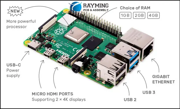
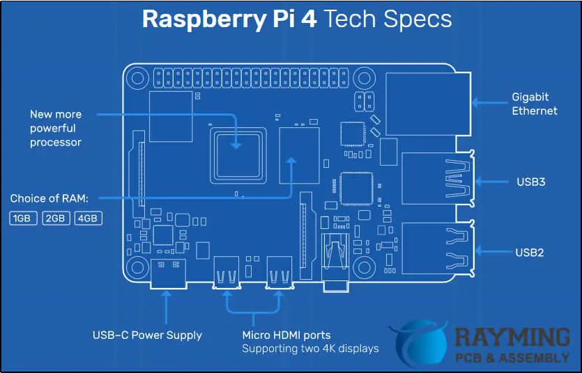
Raspberry Pi 4:
The latest version of the Raspberry Pi series of boards is RPI 4. This is version has some very interesting features like it supports dual 4K displays by means of dual micro HDMI ports. Many advance features are added so that it can work like an actual computer. The RPI-4 software is backward compatible. Whatever you design on RPI-4 will also run on earlier versions.
The RPI-4 is a complete desktop computer. It has an astounding feature of smooth functionality while browsing on internet, documentation or editing, opening multiple tabs of internet explorer and similar work.
This is a more cost efficient machine as compared to common desktop PC and it is very effective. Salient features are high speed networking, Very low noise processing, low energy consumption, support USB 3 and options to choose RAM as you desire.
Support Chrome browser for fast speed, video buffering is good for YouTube and smooth browsing.
The official Raspbian Linux OS. Moreover third party operating systems which can run on RPI are Windows 10 IoT core, RISC, Media Center and Ubuntu. The windows 10 IoT is a limited version of windows 10 and can run single screen app and can support background software running. But still running windows 10 OS on this tiny device is not a good option because of processing power it demands.
Some Important Things to Know About RPI:
Protect it from heat. Keep it in enclosed case. Run official Raspbian OS. Visit RPI website. to get extra help. Do not purchase expensive microSD card 64 GB, just purchase 8GB SD card and install official Raspbian OS and it will fulfill all your needs. It cost around $35 so it can be a good investment. The “Overclocking “mechanism can cause the RPI to run much faster than its defined speed but it can rise temperature that could damage device. The rise in temperature can be countered using heat sink. Software Overclocking does not void warranty.
Applications of Raspberry Pi
The RPIs can perform most of the functions like desktop computer. For example Video Gaming, Media Streaming, Home Automation, Robotics, Internet and Browsing,
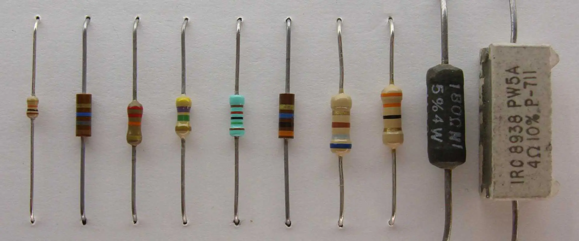
Resistors are one of the most fundamental components used in electronics and electrical circuits. To easily identify resistor values, a color coding system is commonly used to mark the resistance on the body of the resistor.
Learning how to read these color codes is an essential skill for anyone working with electronics. In this comprehensive guide, we will cover:
What resistance and resistors are
Resistor color code systems
3 band
4 band
5 band
Decoding color bands to read resistance value
Calculating resistance from color codes
Determining tolerance from color code
Identifying special values like EIA
Practical examples and exercises
Common mistakes to avoid
Other resistor markings
Frequently asked questions
After reading this tutorial, you will be able to easily decipher the color codes to determine the resistance value of any common resistor. Let’s jump in!
To understand resistor color codes, we first need to understand what resistance means and what resistors are.
Resistance is the property of a material that opposes the flow of electric current. It is measured in ohms and represented by the Greek symbol Ω.
Resistors are electrical components explicitly designed to provide resistance in a circuit. Some key properties of resistors:
Made of resistive materials like carbon, wire windings, metal oxides
Designed with a certain resistance value
Used to limit current flow, divide voltages, damp signals, and more
Available in many form factors like axial, SMD chip, rectangular, etc.
By adding resistors into circuits, we can finely control voltages and currents as needed. But to utilize them properly, we need to know their resistance values. This is where resistor color coding comes in.
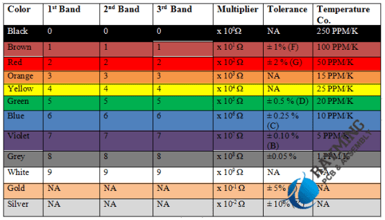
Resistor Color Code Systems
There are a few standards for marking resistance values on resistors with colored bands. Let’s look at the common systems.
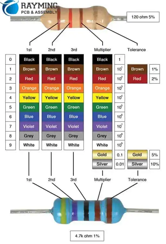
3 Band Color Code
This system uses three colored bands to denote the resistance as follows:<img src=”https://imgur.com/BEnfSfR.png” width=”200″>
1st and 2nd band – Digits for resistance value
3rd band – Multiplier
(Optional 4th band – Tolerance)
For example, green-blue-red equates to a 56 x 100 = 5600 Ω resistor. Very simple and common coding.
4 Band Color Code
This expands the 3 band code by adding a 4th tolerance band:<img src=”https://imgur.com/gBrjaXR.png” width=”200″>
1st band – 1st digit
2nd band – 2nd digit
3rd band – Decimal multiplier
4th band – Tolerance
So yellow-violet-red-gold decodes to 47 x 100 = 4700 Ω with 5% tolerance.
5 Band Color Code
This further expands the code with an extra significant figure digit:<img src=”https://imgur.com/Tbye4Wf.png” width=”250″>
1st and 2nd band – 1st and 2nd digit
3rd band – 3rd digit
4th band – Multiplier
5th band – Tolerance
For example, brown-black-orange-red-gold equates to 10,000 x 100 = 1,000,000 Ω ± 5% tolerance.
This allows expressing higher resistances with greater precision.
The color of the tolerance band indicates the precision of the marked resistance value. Common tolerances include:
Brown – ±1%
Red – ±2%
Gold – ±5%
Silver – ±10%
None – ±20%
Higher precision resistors have tighter tolerances printed on them. For example, a gold band means the actual resistance should be within ±5% of the marked value.
So a 100 Ω ± 5% resistor can have an actual resistance between 95 to 105 Ω. Tolerance gives the acceptable margin of error.
Identifying EIA Values
There is also a special variant of 4-band color codes for EIA preferred values. It is denoted by:
1st and 2nd bands – Standard codes
3rd band – Decimal multiplier
4th band – Gold or silver ±5% tolerance
Gold as 4th band = EIA value x 0.1 Silver as 4th band = EIA value x 0.01
For example:<img src=”https://imgur.com/N5MWUqf.png” width=”200″>
Red-Red-Gold = 22 x 0.1 = 2.2 Ω
Brown-Black-Silver = 10 x 0.01 = 0.1 Ω
Both are standard EIA values. This code helps identify them.
Practice Exercises
Let’s practice decoding some example resistor color codes:
Orange-Orange-Red
Brown-Green-Brown-Silver
Red-Violet-Yellow-Gold
Blue-Grey-Black-Brown
Green-Brown-Orange-None
Scroll down to check your work!
Solutions:
33 x 100 = 3300 Ω
15 x 10 = 150 Ω ± 10% tolerance
27 x 10,000 = 270,000 Ω ± 5% tolerance
68 x 1 = 68 Ω ± 1% tolerance
58 x 1000 = 58,000 Ω ± 20% tolerance
How did you do? With practice, you will be able to read resistor codes effortlessly.
Common Mistakes
Here are some common mistakes to avoid when decoding resistor color codes:
Forgetting the multiplier – Make sure to apply the multiplier band or else your value will be way off.
Mixing up tolerance and multiplier – It’s easy to flip these two adjacent bands by accident. Double check their order.
Misreading similar colors – Red/orange or blue/violet can look alike on small resistors. Take care!
Assuming wrong # of bands – Always confirm the band count before reading the resistor.
Decoding non-standard codes – Some resistors use custom codes. Verify it is a standard scheme.
Faded colors – If bands fade to almost white, they may be indistinguishable.
With experience, you will learn to avoid these pitfalls. When in doubt, check the datasheet or use a multimeter to measure the actual resistance.
Other Resistor Markings
While color coding is the most common, resistors may also be marked in other ways:
Multiplier written numerically such as 10M or 10MΩ for 10 million ohms
Tolerance written out like ±5% rather than color band
3 or 4 digit codes starting with the multiplier e.g. 471 = 470Ω
Actual resistance printed numerically e.g. 10k
SMD resistors marked with just a number string
So you may encounter alternate formats beyond the standard color codes. With practice, you’ll learn to interpret all the common schemes.
Frequently Asked Questions
Here are some common questions about resistor color codes:
Q: Why are colors used instead of just printing the resistance value?
A: The color bands allow cheap, permanent, and unambiguous marking without requiring printed text or symbols.
Q: What do more than 3 bands indicate on a resistor?
A: Additional bands denote tolerance and extra significant figure digits for higher precision.
Q: Why do resistors have a tolerance?
A: Due to manufacturing variations, the actual resistance cannot match the target value exactly. Tolerance specifies the allowable error range.
Q: What is the gold or silver multiplier on 4-band resistors?
A: These denote EIA preferred values. Gold = multiply by 0.1, silver by 0.01.
Q: Can you read a resistor’s value without decoding the color bands?
A: Yes, you can directly measure a resistor’s resistance using a multimeter if you need to confirm its value.
Conclusion
Understanding resistor color coding is indispensable for working with resistors in circuit design and analysis. This guide provided a comprehensive overview of decoding color bands including:
Resistor coding systems – 3, 4, and 5 band
Looking up digit values, multipliers, and tolerance
Calculating resistance from color codes
Identifying EIA values
Avoiding common mistakes
Handling non-standard markings
With this knowledge, you can now easily decipher resistor color codes and determine resistance values. Receiving a handful of resistors is no longer an intimidating puzzle!
Practice reading a variety of example resistor color codes until it becomes second nature. Mastery of these fundamentals will give you confidence working with resistors and building circuits.
DFM stands for Design for Manufacturing. DFM check is the process of analyzing a product design to ensure it can be manufactured efficiently and cost-effectively.
With DFM analysis, engineers examine the design to identify and correct issues before releasing it to production. This avoids costly manufacturing problems down the line.
By the end of this article, you will have a strong understanding of what DFM analysis entails and how it improves manufacturability. Let’s get started!
Increases manufacturability – The design gets tailored to the capabilities of the manufacturing process.
For these reasons, leading engineering teams perform extensive DFM checks before releasing any product to the factory floor. The ROI from avoiding manufacturing issues is tremendous.
When Should DFM Analysis Be Performed?
DFM checks should be performed at multiple stages of the design process:
Conceptual design phase – Early DFM analysis ensures the design direction inherently accounts for manufacturing best practices.
Detailed design phase – Rigorous DFM checks should be conducted once the detailed design is frozen before release to production.
Design revisions – DFM checks also needed whenever design changes are made to ensure no new issues are introduced.
In general, DFM checks should be an ongoing process throughout development rather than a one-time step at the end. Issues caught early in design iterations can prevent costly changes later down the line.
For complex products, DFM checks may be performed by a dedicated manufacturability engineering team. They take the designer’s CAD model and run intensive DFM analysis on it as a service.
No matter the design phase, integrating DFM as early and often as possible is key for optimizing manufacturability.
Major Areas Analyzed in a DFM Check
DFM analysis involves assessing the design from multiple aspects that impact manufacturing. Here are some of the major areas checked in a DFM review:
Tolerances
Tolerance stackups calculated to ensure parts will fit together within specified range
Tolerances not too tight for process capabilities
Statistical tolerance analysis conducted where possible
Clearances
Sufficient clearances between components for material thickness
Adequate clearances to access assemblies and fasteners
Clearances checked for operation without interference
Minimum electrical clearances met
Draft Angles
Draft angles added on vertical faces to ease ejection from molds
Uniform draft angle between adjacent faces
Adequate draft for deep/high parts and materials used
Hole Sizes
Hole diameters meet tap drill sizes for specified thread types
Hole sizes account for plating tolerances if plated
Large holes have web thicknesses for required strength
Finishes avoid tight textures causing friction or galling
Radius surface finishes specified where needed
Heat Sinks
Heat sinks sized properly for heat load and air flow
Thermal interface material thickness considered
Fins aligned with air flow direction
Welds
Weld types appropriate for materials and joint design
Gaps provided for welding access
Distortion from weld process and sequencing minimized
Part Symmetry
Parts designed symmetric where possible to avoid orientation concerns
Non-symmetric parts clearly identified in drawings
Stamping and Forming
Draw depths and minimum radii suitable for material thickness
Bend radiuses checked for sheet metal parts
Stamping web widths adequate for strength
Molding
Draft angles provided on molded parts
Radii added to corners to ease fill
Core pins accessible and adequate for details
Undercuts eliminated unless using collapsible cores
Casting
Casting draft present with proper direction
Minimum thicknesses to avoid porosity observed
Appropriate finish allowances specified
Fastening and Joining
Fastener sizes appropriate for materials and assemblies
Fastener spacings meet engineering requirements
Adhesives and press fits designed for required strength
Part Handling
Points identified for safe automated part handling
Low friction surfaces checked where automated sliding occurs
Weight limits observed for manual lifting and ergonomics
Assembly Sequence
Efficient tabs snap features used where helpful
Conditional assembly sequences enabled where needed
Assembly performed from stable datum points first
Test and Inspection
Test points provided to verify full assembly
Key dimensions defined for in-process inspection
Go/no-go assembly checks incorporated
This covers some of the major areas scrutinized during a thorough DFM analysis. The full scope depends on the specific design and manufacturing process.
While checking the above details, DFM engineers are guided by fundamental DFM principles that influence the overall manufacturability of a design:
Simple and Intuitive
Design should be as simple as possible while still meeting functional needs
Avoid unnecessary complex geometries and mechanisms
Intuitive assemblies are easier to manufacture correctly
Error Proofing
Incorporate go/no-go checks to prevent incorrect assembly
Include guides, keys, and asymmetry for foolproof assembly
Eliminate ways to assemble incorrectly through smart design
Standardization
Maximize use of standard parts, materials, processes
Follow industry and in-house standards where possible
Process Capabilities
Stay within known process capabilities -avoid pushing limits
Account for inherent process variation in tolerances
Modularity
Break complex designs into self-contained modules
Standard interfaces between modules for flexibility
Modules can be made and tested independently
Consolidation
Combine parts into single parts where possible
Avoid unnecessary joints/fasteners to consolidate
Handling
Design parts to be easily handled and positioned
Add fiducials and other features to assist automation
Service and Repair
Enable access to lifecycle maintainable components
Fasteners, connectors, etc. designed for serviceability
By adhering to DFM principles like these, engineers can design products with manufacturing in mind right from the start. This flows into all the detailed checks conducted later.
Performing Manual vs Automated DFM Checks
DFM analysis is traditionally conducted manually by experienced engineers trained in manufacturing processes. However, automated DFM checking software has also emerged to supplement manual review.
Manual DFM Checking
With manual DFM analysis, engineers use their expertise to:
Visually inspect CAD models for issues using a checklist
Calculate key dimensions, stacks, and clearances by hand
Simulate assembly sequences to validate manufacturability
Judge surface finishes, drafts, radiuses by sight
Suggest design changes to fix found issues
Manual checking taps into an engineer’s manufacturing knowledge. But it can be tedious and prone to human error.
Automated DFM Checking
DFM software automatically checks models for common issues like:
Insufficient draft angles on faces
Tight component clearances
Hole dimensioning errors
Thickness and radius violations
Interference detection
Standard violation checking
Automated tools provide consistent, rapid analysis. But software cannot fully replace an engineer’s judgement and insight yet.
In practice, the two methods are combined – engineers first run an automated DFM analysis then manually review the flagged issues. This gives the best results.
Fixing DFM Violations
When issues are identified from DFM checks, the designer needs to modify the CAD model to address them. Here are typical ways DFM violations are fixed:
Relaxing tolerances – Increase tolerance windows to viable ranges
Changing dimensions – Resize parts and geometry to meet requirements
Adding draft – Add or increase draft angles where lacking
Altering surface finishes – Change surface specs to better finishes
Revising hole features – Modify hole sizes to suit tap sizes or add webbing
Adding clearance – Provide adequate clearance between components
Eliminating undercuts – Remove undercuts in molded parts through design changes
Changing joinery – Revise joints, fasteners to improve assemble-ability
Simplifying geometry – Simplify complex shapes to the basic functional geometry
Separating parts – Break convoluted parts into simpler individual parts
Refining assembly sequence – Optimize assembly steps for efficiency and clarity
Usually, many small changes are required versus one major redesign. The designer iterates to incrementally improve the design based on the DFM feedback.
Frequently Asked Questions
Here are some common questions that arise regarding DFM analysis:
Q: When should DFM analysis be done – by designers or by manufacturing engineers?
A: DFM principles should first be applied during the initial design phase. Later extensive DFM checks can be done by manufacturing engineers as an independent quality check.
Q: What are some limitations of automated DFM analysis tools?
A: Automated tools miss context-specific issues and have limited capability to suggest fixes. But they rapidly find basic issues like insufficient drafts.
Q: How is DFM analysis different for machined parts versus plastic injection molded components?
A: Each process has unique DFM considerations – for machining, avoid thin walls, deep pockets, and surfaces hard to reach with cutters. For molding, check drafts, radii, tolerances.
Q: What is the right level of detail for a DFM analysis?
A: It depends on the design complexity, production volume, cost, lead time, and other factors. Higher volume or cost products warrant extremely exhaustive DFM review.
Q: Is DFM analysis applicable beyond mechanical and physical product design?
A: Yes, the principles of optimizing a design for ease of execution extend to many fields. DFM concepts are relevant even in UX design, process design, and more.
Conclusion
DFM analysis is a critical step in optimizing a product design for manufacturing and assembly. By thoroughly checking key areas like tolerances, clearances, surface finishes, and reviewing the design from a manufacturing perspective, engineers can catch and correct issues early.
Performing DFM checks systematically at each stage of design, incorporating both automated tools and manual review by experienced engineers, results in the highest quality analysis. The ROI from avoiding manufacturing problems is well worth the effort invested into rigorous DFM practices.
With the methodology and best practices covered in this guide, you now have strong knowledge of what an effective DFM analysis entails. Leverage DFM practices in your organization to save costs, reduce defects, shorten time-to-market, and ultimately create products optimized for manufacture.
Free of Cost DFM Check
DFM (Design for Manufacturing ) is known as file check and it is basically an added value service that most of PCB manufacturers offer. The services of DFM are related to the checking of PCB design for any possibility of issues which may hinder the process of PCB manufacturing and fabrication. In case if any issues are sorted, customers are got in touch on immediate basis and issues are resolved at higher priority and fabrication of PCBs is arranged accordingly.
The DFM check offered by RayPCB is cost-effective of the system we use for DFM check is an autonomous way for enabling the manufacturing and fabrication system of PCBs hassle-free and sort out issues which cause trouble. The autonomous system of FDA check is known as Valor DFM. The system helps in lowering cost of PCB and saves time as well. The DFM is conducted on the basis of five aspects at RayPCB known as single layer and mixed layer checks, silkscreen checks, drill checks, and ground/power checks. The details are given below.
The action of drill checks is for finding out the potential defects which may hinder the manufacturing process in different layers of PCB. Statistics are generated on drill layers. The drill checks is supposed to be operated on drill layers only. It is using drill stack, bottom and top layers along with ground or power layer in stack. The checklists are given below.
Items
Functionalities
Ground/Power Shorts
It reports the drills which are touching copper nets of more than ground or power layer.
The mixed and single layered checks is designed for finding potential manufacturing defects and generation of statistics in mixed and single layers. The action is dedicated for single layers, however it can also be implemented on mixed and other layers. The main checklist are given below.
Items
Functionalities
Size
It has information of the size of pads, text, arcs, line neck downs, vias, shaved arcs, and shaved lines.
Stubs
It has information of endpoints of unconnected lines.
Spacing
It has information of the violations among nets and circuits of pads among text, shorts, and spacing among CAD nets and non-touching features of CAD.
Silver
It has information of the silver lines among pads and lines.
Route
It has reports of the displacement violations among pads and edge of route.
Drill
It has information of the displacement among vias, NPTHs, PTHs, Pads, rings, Circuits, and copper etc.
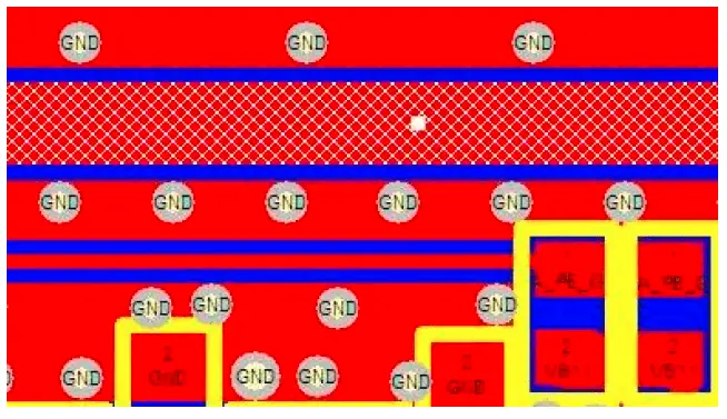
3. The Ground/Power Checks:
The intentions of the ground/power checks is to have an identification of the manufacturing defects in ground and power in mixed layers. It has utilization of various algorithms for diagnosis of positive and negative power along with ground layer. Checklist is given as follow.
Items
Functionalities
Route
It has report of the closed spacing among route and copper features.
NFP Spacing
It has information of spacing among NFP-planes, and NFP-NFP.
Drill
It has information of distance violations among vias to plane, annular rings, clearance, and copper etc.
Plane Spacing
It has information of spacing among various features of planes.
Thermal
It has information of spoke reduction and width of the connectivity of thermal pads.
Plane Width
It has reports of inadequate width of the layer of copper among 2 drills which are connected on copper plane.
It has information of features of outside and inside as well as keepout and keepin areas.
Plane Connection
It has reporting of the detached areas of copper which are utilized as reference planes and are in design which are causing unreferenced net or missing electrical connection.
This function is for checking layers of solder masks for any potential manufacturing defects. The layers of solder masks are considered negative and the positive features are describing clearance of the solder masks. The function is also checking the solder paste which is deposited on the pads. This function is operating on single layer solder mask and below is its major checklist.
Items
Functionalities
Spacing
It has information of the spacing among clearance.
Extra
It has a reporting of soldering mask features which are lacking copper pads and are not intersecting each other.
Drill
It has reporting of close distant to solder mask opening of NPTH annular rings.
Bridge
It has information of pads which are there without solder mask.
Silver
It has reports of the silvers among clearance and solder mask.
Missing
It has reports of the missing clearances.
Coverage
It has information of lines which are too close to clearance.
Pads
It has reports of the opening of distance to solder mask of pads comprising of undrilled pads. It has information of special group as well such as gaskets, information of width of solder mask etc.
This function has an intention of finding potential manufacturing defects present in layers of silkscreen and also generation of statistics. This function is only used for checking silk screen layers because it has a reliance on job matrix related to external copper, layers of drills and solder mask. Below are details of checklist.
Items
Functionalities
String Overlap
It has information of intersection or touching of silkscreen with various string values.
It has information of spacing among clearance of solder mask and silkscreen features.
Hole Clearance
It has information of spacing among drills and silkscreen features.
Line Width
It has information of the violations of width and length to its respective ratio.
Route Clearance
It has information of spacing among route features and silkscreen features.
You can avail advantage of DFM free check offered by RayPCB right away. Don’t waste time and contact us right now for availing this amazing deal of free DFM check.
Printed circuit board (PCB) design requires specialized software tools to lay out connectivity and translate circuit schematics into physical board fabrication. Many solutions are available for PCB designers. This article outlines the top 8 PCB design software options based on popularity and capabilities.
Selecting among these top options depends on specific project needs and team experience.
Important PCB Software Considerations
Beyond core schematic and layout capabilities, key considerations when choosing PCB design software include:
Cost – How the pricing fits within your budget. Perpetual license, subscription, free?
Learning curve – Match software complexity with team experience level.
EDA environment – Integration with other tools like simulation for a unified workflow.
Libraries – Availability of extensive component libraries frees designers from creating footprints.
Scalability – The ability to handle everything from DIY to enterprise-level designs.
Output generation – Does it support manufacturing requirements like Gerber, IPC netlists, BOM?
Matching software strengths to the organization and application maximizes the benefit.
Integrated PCB Design Software Environments
Many EDA vendors offer integrated design environments spanning simulation, PCB layout, and physical verification:
Cadence Allegro + OrCAD + PSpice
Tight integration for schematic-based simulation and PCB design
Covers range from entry level to advanced tools
Mentor Xpedition + PADs + HyperLynx
Unified PCB design workflow with analysis under one interface
Scales individual to enterprise-wide needs
Altium + Altium Designer
Single solution from schematic through manufacturing
Additional tools for FPGA and embedded development
Using tools from one vendor improves design workflow and data exchange while providing a convenient single vendor support point. But beware of vendor lock-in limiting future options.
Cloud-Based PCB Design
Many EDA software companies now offer cloud-hosted options:
Benefits
Reduced IT infrastructure needs
Usage-based pricing model
Automatic updates
Access designs from anywhere
Limitations
Requires reliable high-speed internet
Potential for latency during editing
Information security concerns
Vendor dependent
Cloud-based tools facilitate collaboration but may not suit every design scenario.
Open Source PCB Design Software
In addition to KiCad, open source PCB design software options include:
gEDA – Full suite of EDA tools focused on open collaboration
HorizonEDA – Web-based schematic and layout tool
PCBWeb – Browser-based editor for simple boards
Fritzing – Emphasis on DIY and maker community
Open source provides free access but typically lacks vendor support and advanced capabilities. The open approach facilitates customization and community development.
Evaluating PCB Design Software
When selecting a PCB design solution:
Review product brochures and feature lists
Compare pricing tiers and availability of educational licenses
Join online user forums to research experiences
Download trial versions to experiment firsthand
Seek feedback from colleagues
Contact vendor sales teams
Taking time to thoroughly evaluate software against requirements ensures the optimal choice long-term.
Training Resources
Extensive training resources are available for most leading PCB software:
What is most important when comparing PCB software?
The core layout and routing capabilities are essential, but also consider learning curve, integration, output generation, and other productivity factors.
Which is better – perpetual license or subscription model?
Subscriptions allow flexible scaling and updating but require ongoing payments. Perpetual licenses require large upfront costs and additional purchases for upgrades. Evaluate total long term cost.
Is cloud-based PCB software more efficient for teams?
Cloud tools facilitate real-time collaboration, but designers must be comfortable with cloud security policies and inevitable internet dependencies.
Should I use the built-in autorouter?
Built-in autorouters provide a starting point but generally can’t match the quality of manual routing for complex designs. Use judiciously.
Can students or hobbyists access professional tools cost-effectively?
Many leading vendors offer free or discounted educational licenses, sometimes limited in capabilities. Student versions can provide advanced tools for learning prior to entering industry.
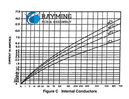
When designing printed circuit boards (PCBs), the width and thickness of copper traces impact how much current they can safely carry without overheating. Traces must be appropriately sized based on expected current levels. Copper weight, trace width, and current capacity have a direct mathematical relationship. This article provides an in-depth examination of these parameters and their correlation in PCB design.
Copper Weight
Copper weight refers to the thickness of the copper foil used to form PCB traces, pads, and planes. The most common weights are:
1 oz – 1 ounce per square foot, equivalent to a thickness of 1.4 mils (34 μm)
2 oz – 2 ounce per square foot, equivalent to 2.8 mils (68 μm)
Heavier copper foil allows for higher current capacity. But it costs more and can complicate fine-pitch PCB fabrication.
Trace Width
Trace width is the manufactured width of a PCB track, typically measured in mils (1 mil = 0.001 inches). Wider traces can handle more current due to reduced resistance. Minimum widths are dictated by current levels.
Current Carrying Capacity
The current carrying capacity defines how much continuous DC or RMS AC current a trace can conduct without exceeding temperature limits, usually 10-30°C above ambient. Excess current causes overheating damage.
Factors Affecting Current Capacity
Current capacity depends on:
Copper weight – Heavier copper has lower resistance
Trace width – Wider traces have lower resistance
Temperature rise – Allowable increase over ambient
Environment – Operating temperature influences limits
Heat sinking – Thermal dissipation enables higher current
Appropriately sizing traces for expected currents prevents overheating while minimizing unnecessary PCB space and cost.
Copper Weight and Resistance
The primary factor relating copper weight to current capacity is the change in electrical resistance:
Heavier copper has lower resistance
Lower resistance results in less heating from a given current
Reduced heating allows higher current capacity
For example, the table below shows typical per-length resistances relative to common copper weights:
Copper Weight
Resistance (ohms/mm)
1/2 oz
0.0048
1 oz
0.0029
2 oz
0.0016
The resistance drops as copper weight increases, enabling higher current capacity.
Calculating Resistance from Weight
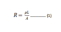
The resistance through a length of conductor is calculated using:
Where:
ρ is the resistivity of copper (1.678 x 10<sup>-8</sup> Ωm)
L is the length (m)
A is the cross-sectional area (m<sup>2</sup>)
For a rectangular PCB trace, the cross-sectional area is:
Where:
W is trace width (m)
T is copper thickness (m)
Combining the equations allows resistance calculation based on trace dimensions and copper weight.
Trace Resistance Example
For a 50 mm long, 0.5 mm wide trace in 1 oz (34 μm) foil:
Increasing to 2 oz (68 μm) thickness halves the resistance:
Heavier copper foil significantly reduces electrical resistance due to the larger cross-sectional area.
Lower Resistance Increases Current
The power dissipated as heat in a conductor is:
Where I is the current and R is the resistance.
For a given temperature rise, higher current is possible with lower resistance before reaching power dissipation limits. The reduced resistance of thicker copper enables higher current capacity.
Trace Width and Resistance
In addition to copper weight, trace width also impacts resistance:
Wider traces have a larger cross-sectional area
Larger area produces lower resistance
Lower resistance allows higher current capacity
For example, a 100 mm long trace with 0.25 mm width has 4X the resistance of a 0.5 mm wide trace in the same 1 oz copper:
Wider traces reduce resistance and enable increased current carrying capacity.
Combining Weight and Width
The effects of copper weight and trace width are multiplicative. For example, the combination of:
Doubling copper weight from 1 oz to 2 oz (halves resistance)
Doubling trace width from 0.25 mm to 0.5 mm (halves resistance again)
Decreases resistance to 1/4 of the original, increasing current capacity by a factor of 4X.
Optimizing both copper weight and trace width provides the maximum current capacity for a given PCB area.
Trace Temperature Rise
While lower resistance allows more current, we must also consider the resulting temperature rise. Power dissipated as heat raises trace temperature:
Lower resistance allows increased current capacity
Wider traces also decrease resistance due to larger area
Trace width must be sized based on target current
IPC-2152 tables relate width and weight to current capacity
Heat sinking improves capacity for a given trace size
Matching trace size to current prevents overheating damage
Correctly correlating copper weight, trace width, and current carrying capacity ensures safe and reliable PCB performance under expected current loads.
Frequently Asked Questions
How accurate must current capacity calculations be?
Rough estimations are often sufficient early in design to determine minimum widths. More detailed analysis may be warranted for high-power or long-life applications.
What copper weight should be used?
1 oz copper offers the best balance of cost, manufacturability, and performance for most applications. 2 oz provides higher capacity for high-power boards.
Is it always better to use thicker copper?
Not always – thicker copper increases material and fabrication costs. Use the minimum weight that satisfies capacity needs. Excessive thickness can also lead to thermal stresses.
How much margin should be added to current capacity?
A 10-20% margin above calculated capacity is recommended to account for analysis inaccuracies and environmental variations during operation.
Can vias decrease current capacity?
Yes, narrower vias can create bottlenecks increasing resistance and heating. Size vias at least as wide as connected traces to prevent reductions in capacity.
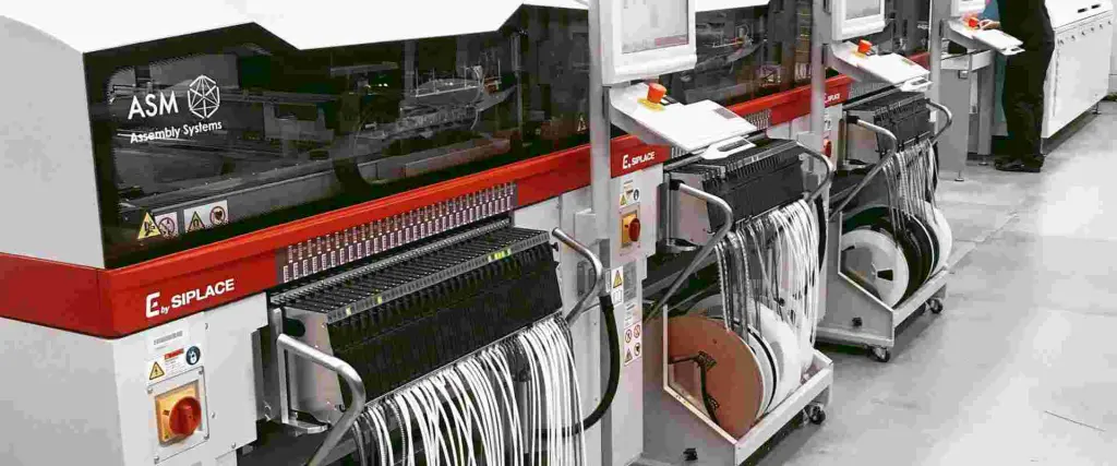
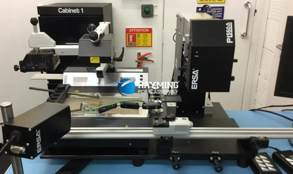
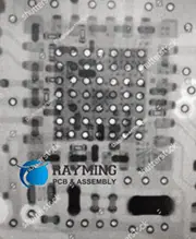
SMT inspection is the process of verifying the quality and accuracy of surface mount technology (SMT) printed circuit board (PCB) assemblies. It involves using automated optical inspection (AOI) systems and other methods to check for defects in SMT components and solder joints. Thorough SMT inspection is crucial for ensuring the reliability and performance of electronic devices and equipment. This article provides an overview of the key aspects of SMT inspection.
SMT Assembly Overview
SMT is a PCB assembly method where components are mounted directly onto the board surface rather than through holes. The main steps in SMT assembly are:
Solder paste application – solder paste is printed on pads
Common SMT components include resistors, capacitors, integrated circuits (ICs), connectors, LEDs, and many other types.
Importance of SMT Inspection
Inspection of SMT PCB assemblies is critical because defects such as:
Missing components
Wrong component orientation
Incorrect component values
Shifted components
Insufficient solder
Solder bridges
Can lead to circuit malfunctions, equipment failures, and reliability issues if not detected. SMT inspection finds these defects and ensures assembly quality.
There are several key methods for inspecting SMT assemblies:
Automated Optical Inspection (AOI)
AOI systems use advanced cameras and software to automatically check assemblies for defects. This is the primary SMT inspection method.
In-Circuit Testing
Electrically tests circuits to verify component values and find assembly faults like shorts or opens.
X-Ray Inspection
Uses X-ray imaging to check component placement, especially for hidden or packaged parts.
Manual Visual Inspection
Human operators visually examine assemblies under microscopes for defects. More time-consuming but finds subtle issues.
AOI Inspection Overview
Automated optical inspection provides thorough and efficient quality control for high-volume SMT production:
Uses cameras to capture PCB images
Software analyzes images comparing to CAD data
Checks component placement, orientation, skew
Verifies pad printing quality and solder volume
Finds common defects and quantifies pass/fail rate
Generates reports showing inspection regions and results
AOI inspection can be done after solder paste printing, after component placement, after reflow, and at various stages depending on the process. Post-reflow AOI is most common.
AOI Inspection Systems
AOI systems consist of:
3D Sensor Cameras
High resolution and precision 3D sensor cameras with different magnification levels capture PCB images.
Top and bottom side cameras for double-sided inspection.
Identifying process improvements based on findings
Tracking corrective actions taken to resolve issues
Inspection documentation provides production feedback to prevent repeated defects.
Summary
SMT inspection using AOI, manual, X-ray, and electrical methods is essential for quality control.
Automated optical inspection delivers rapid, accurate, and repeatable defect detection.
Manual inspection complements AOI to find subtle and functional issues.
Inspection metrics feedback into process improvements to reduce defects.
Documentation of inspection results provides traceability and preventive action data.
Effective SMT inspection is crucial for achieving high assembly yields and reliability.
Rigorous inspection practices are key to successful high-volume SMT electronics manufacturing.
Frequently Asked Questions
What is the most important SMT inspection?
Post-reflow AOI inspection after soldering provides the best assessment of true assembly quality and reliability. It finds both component and solder joint defects.
How often should AOI programs be updated?
AOI programs should be updated whenever the PCB design changes significantly. Small revisions may only need minor program adjustments. Updating programs ensures accurate inspection as designs evolve.
Does AOI replace manual inspection?
AOI augments but does not replace manual inspection. AOI provides fast and repeatable automated checking, while manual inspection finds subtle issues missed by automation. The two methods work together for complete quality control.
Can AOI detect all solder joint defects?
While very capable, AOI may still miss some solder defects like small voids or cracks. Additional manual inspection is recommended to complement AOI, especially for critical high-reliability solder joints.
Is X-ray or AOI inspection better?
AOI is lower cost and faster, but X-ray provides unique capabilities such as seeing hidden solder joints or inside packaged components. Applications with dense components favor X-ray, while high-throughput consumer products are better suited to AOI.
PCB Inspection in SMT assembly process: ICT, AOI and AXI
While technology continues to move towards increasing levels of complexity, it is increasingly necessary to improve quality control processes before, during and after manufacturing processes. Other types of tests, such as Automated Optical Inspection (AOI) and X-ray Automated Inspection (XAI), have been added to the traditional In-Circuit Testing (ICT).
When choosing which method or combination of test methods we will use, the level of complexity of the PCB is taken into account, what is the PCB Manufacturing process that predominates in it, as well as what is the purpose of the analysis we are conducting.
In-Circuit Testing (ICT)
The ICT (In-Circuit Test) allows us to search for different type of failures such as opens, shorts, continuity tests, etc. There are two main techniques for it.
This is the traditional exam. It seeks to generate multiple contact points in the circuit through small spring loaded pogo pins, which seen from afar maintain the similarity with a bed of nails and hence its name. Each pogo pin will make contact with a cricut node, this way a pressure is applied to the Device Under Test (DUC) and hundred of connections are simultaneously tested. Using this technique we can find component defects, also search for parameter deviation, solder joint bridging, displacement, opens, shorts, continuity tests, etc.
This type of test is suitable for simple PCBA and also for mass production systems, has a low cost and is fast. However, if we try to apply it to high-density components or large-scale integration PCBs in which miniaturization has taken a leading role, we will find that there are technical difficulties that cannot be overcome. For this reason, over the years, alternative techniques have been developed for this type of test.
This technique allows us to perform tests with smaller sizes, we can achieve a min test pitch up to 0.2 mm. The PCB is introduced in a test environment in which the different probes will come into contact with the pads and vias. We can analyze it searching for shorts and opens, but also the system is equipped with a camera that analyzes the shape of the electronic components and their size. It allows us to control if elements are missing. Is also capable to allows us analyze the value of the components as resistance and capacitance, for instance. It is also possible to analyze the polarity of the elements.
An AOI inspection will allow us to analyze assembly and manufacturing failures. The PCB is analyzed by one or several cameras, these images are then compared through the software with a board that is taken as a parameter usually called “golden board” or with design specifications.
This type of analysis is usually performed at the end of the assembly line to ensure the final quality of the PCB. Some Pick and place machines use this technology to avoid defects in the placement and alignment of components.
Therefore, another fundamental aspect is that it allows us to track processes.
It allows us to monitor the prototype pcb assembly process and then classify and correct displacement and component assembly defects.
Usually the AOI equipment is placed in different stages of the assembly line so that the specific manufacturing situation can be monitored online and the necessary basis for the adjustment of the manufacturing technique is provided.
We can mention three important places to consider:
Before the application of solder paste. This will allow to control that the amount of paste applied is exact, neither more nor less. We can also avoid the lack of alignment by placing it, as well as welding bridges between pads. It is also important to configure an AOI control point Before the reflow soldering process, in this way we can ensure that the components are placed correctly before completing the soldering process.
Finally, of course, also after reflow soldering. This provides an overview of the process that allows to identify faults in both the last and previous stages.
The application of X-ray technologies to PCB inspection is a powerful tool for analyzing failures, especially for soldering analysis. It allows us to observe the inside of the solder and discover if there is a lack of filling, bubbles, etc. In PCBs where BGA technologies are present, it becomes essential because we cannot observe the solder joints made under the chip.
An X-ray inspection will allow us to observe the soldering inside and under the chip, analyzing if all the connections have been made correctly. 2D, 3D technologies are used to perform image analysis.
2D inspections look for cracks, bridges, poor alignment or also insufficient solder. This is the low cost option. There is also the option of X-ray inspection in 5D, here we compare the images obtained from the PCB with a CAD file for the differences. Using this inspection method we can make three individual cuts between the BGA and the solder balls, also enter the solder balls and evaluate in depth the connection between the balls and the pad. Therefore, using this technique our engineers may find faults that would be impossible with another technique.
So, what inspection method choose? ICT, AOI or XAI?
First, we must consider that we do not have to choose between them, but we must understand for what we will use each of them, how and when to combine them. This will depend on the level of complexity of our PCB and also on the type of fault we are looking for.
It is important to be clear about what type of failures each type of inspection can detect. This table shows us this clearly.
Notice that some errors can only be detected through ICT, so this test becomes indispensable.
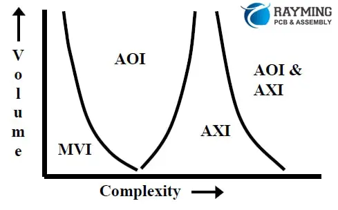
Therefore, our choice of options will be between using AOI, AXI or combining them. As a general recommendation we can take the graph presented here. It should be noted that a PCB may not be complex, but include BGA devices and remember the above: if we have a BGA component, only X-ray technology allows us to analyze in detail. MVI stands for Manual Vision inspection.
We must also bear in mind that time is money and XAI is a slow inspection technology compared to AOI, with which pcba cost will be higher.
As a final conclusion, we must say that it is always advisable to conduct an ICT. In addition, although the cost of the application of XAI inspections is higher, there are PCBs in which we cannot stop doing so due to the presence of BGA components and also because some soldering failures only XAI is able to detect them. A combined use of all techniques will dramatically reduce process failures and scrap.
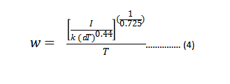
A PCB trace width is simply a parameter defining the distance covered across a circuit board’s trace. Some other well-known parameters here include trace thickness and spacing. Four major factors influence the PCB trace width. These include:
The capacity of the trace necessary to carry current
PCB Trace Width Calculator: What does this mean?
No matter the type of industry you work in, every day you may use a printed circuit board. These devices are very important to how electronics function. Also, they connect and offer mechanical support to electrical components. This is to ensure that they operate properly.
When utilizing Printed Circuit Boards to sustain computers, lighting technology, or medical equipment, they must operate with the right trace width. Using a circuit calculator, you will be sure of the safety of your printed circuit board. They will also stay functional all the time.
The use of the IPC-2221 standard is the major factor in the derivation of a PCB trace width calculator. This standard helps in calculating the conductive track width of a printed circuit board (PCB). It is advisable that you design the PCB traces in order to bear the highest current load even before they start malfunctioning.
The determination of the copper width calculation, at a specific thickness, is necessary. This helps in allowing the transfer or movement of a particular current value. In addition, the copper thickness and width need to be enough to help maintain the rise in temperature at levels below the input.
How to get Trace Width Making Use of a PCB Trace Width Calculator
PCB Trace Width Calculator
This calculator needs the imputation of some values to know the trace’s desired width. The representation of this width is in mils & deals with the utilization of some values. These include:
The conductive layer’s area, which is usually in mils square
The trace’s thickness, which is in ounces/sq ft
What differentiates the External vs. Internal PCB Trace Width Calculators?
Internal PCB trace width calculators are tools that determine the required width of an internal trace. The determination of this internal trace width is to help carry a specific current amount.
External PCB trace width calculators are similar tools, which tell an external trace’s width. The result of the trace width also, is useful for the transfer of the current of a particular amount.
Consequently, the difference seen between the external and internal traces has to do with their location. This location relates to the substrate of the board.
Why is Using a PCB Trace Width Calculator Important?
During the production of PCBs, you will discover that the limitations of current-carry are a major constraint.
You may trace a PCB successfully and then later discover that it will not be able to carry the needed amount of current effectively. Consequently, the printed circuit board’s intended application experiences a setback. This is due to the inadequate current capacity.
Making use of your PCB trace width calculator ensures the conductance of the right current value. Using this circuit calculator, you may utilize the highest current rating you desire to know the width of your trace.
In addition, you may influence the rise in temperature which your PCB records. This is possible by making use of your PCB trace width calculator.
More Facts about the PCB Trace Width Calculator
Engineers often utilize the PCB trace width calculator in the fabrication process of a PCB. This tool helps to detect a lot of things in a circuit board. Before fabricating a PCB, you need to understand how the element works. Other important things you need to know about this tool are discussed here.
It is very important you detect the conductive layer’s area. You can use some constant values to determine this area. The IPC-2221 can help you to derive the constant values which are b, k, and c. These values vary depending on the location of the trace. The location of the trace can either be internal or external. The values of these constants are requirements for conductive material.
Detecting the temperature of the trace helps to know your PCB’s thermal performance. This plays a significant role in knowing the important properties of a PCB. You can sum the highest desired increase in the temperature. This will help you to get the overall temperature trace. The values of the temperature are in °C.
The PCB trace width calculator has a mil. This mil plays a vital role. In the PCB world, mil is a terminology. It is frequently used when talking about the thickness of the circuit board layer. For instance, you can express copper thickness in ounces and as well as convert it to mils.
You don’t need the trace width to determine dissipated power and the voltage decrease. However, you need to understand the resistance value and the value of maximum current. This will help to tell or reveal the loss of power and voltage drop.
Use the overall resistance value and the maximum current value to get voltage drop. Multiply the maximum current value’s square and the value of resistance to get the power loss. All of these things should be taken into consideration. This will help calculate the voltage drop and the dissipated power.
What Does It Mean To Experience a Rise In Temperature When Calculating The PCB Trace Width?
When there is a flow of current via a conductive trace, there is a generation of heat. This is a result of the resistance it gives to the conductor’s flow of current.
The increase in temperature defines the generation of heat. We refer to this as the rise in temperature. Also, you may determine how much rise in temperature your PCB will be able to sustain. This is possible by making use of a PCB trace width calculator.
When you provide PCB trace widths that are wider, you will be able to reduce the buildup of heat. This then results in a rise in temperature.
For many printed circuit boards, a temperature rise of 10 degrees is safe. Otherwise, you can fabricate boards to withstand a higher value in temperature rise. Also, you will find the application’s environment. This will help influence the board’s overall temperature.
Can You Extract Other Measurements By Using the PCB Trace Width Calculator?
PCB trace width calculators allow you to be able to establish different PCB measures. You can include additional input parameters. These include the trace’s length and the temperature for operation. This helps to extract additional measurements. Due to this, you can determine the measures below.
The power dissipated along the trace
A drop in voltage across the pcb trace
The trace’s resistance value
The trace’s rise in temperature
Can Board Spokes Be Subject to Trace Width Calculation?
They look like traces. However, they have a short length and are usually inserted inside the plane. Whenever you are making use of a trace width calculator, people hardly consider the spoke. This is because not all printed circuit boards have them.
It is however compulsory to ensure that spokes have a reduced width compared to actual traces. This is done without basing it on calculations.
Can we regard the Cross sectional Area of the Conductive Layer as an Important Parameter in Calculating a PCB Trace Width?
Yes, this is a very important parameter. The conductive layer’s cross sectional area is a very significant input when ascertaining the PCB trace width calculator.
This area in question is given in mils squared. This area is useful as the numerator for the calculation of the division of the trace width.
Determining the conductive layer’s cross sectional area requires some parameters. These parameters are highlighted below.
The maximum rise in temperature permitted which is in °C
Three constants c, b, and k are different when there are external or internal traces.
The maximum current permitted which is calculated in Amperes
Can the PCB Trace Width Calculator Detect the Trace Resistance?
To get your trace’s resistance value, you can make use of a PCB trace width calculator. PCB engineers have to calculate the trace width to know the value of resistance. The below parameters is needed for the trace width:
The trace length in centimeters
The overall or total temperature of trace
The trace thickness measured in ounces/ sq ft
The conductive layer’s cross sectional area
The conductive material’s resistivity value
Calculating the current-carrying capacity
Calculating the current of the trace width of a PCB is very important. You can achieve this by using different methods. There is a method that utilizes a circuit calculator that determines the current of a PCB trace. Another method utilizes the PCB width calculator.
It is very important to detect the current carrying capacity of the board. You need it when you have to evaluate the application limit of the board. Knowing the current limitations of the PCB trace width is important. It will help you to prevent exposing the circuit boards to possible damaging use.
What Determines Maximum Current-carrying Capacity?
The cross sectional area of the trace often determines the current carrying capacity. The temperature rise is also important. The trace’s cross sectional area is directly proportional to the copper thickness. The same goes for the trace width.
To get the maximum carrying capacity, you need a simple formula. Some practical cases are not easy to calculate. This is due to the rise in temperature and cross sectional area. Other things also determine the current carrying capacity of the trace. These things may include vias, components, and pads.
Traces that have many pads will function more than ordinary traces. Engineers place circuit boards on some trace between pads. This happens when there is abundant solder paste on pins or components. When this occurs, it results in an increased cross sectional area. Increasing the trace width provides a solution to this problem.
When you can’t widen a trace, you can apply a solder mask on traces. The surface Mount Technology procedure needs solder paste. Trace width will increase after reflow soldering. This will help the current carrying-capacity to also rise.
One can get the trace current carrying capacity of a PCB using a formula. This application is ideal for straightforward trace calculation. It is important to consider contaminant pollution in the fabrication of a PCB. Pollution can result in the breaking down of some traces. There must be a security factor to prevent the issue of overloading.
Engineers also need to pay special attention to turning traces. If there is an acute angle in a trace, there will be a non-smooth transfer. This can have an effect on small traces or current with a large width. However, when the current-carrying capacity is low, there might be issues.
What is the difference between external and internal trace widths?
People wonder how to differentiate between the external and internal traces. You can know the differences through their location. Internal traces are PCB’s inner layers while external traces are on the outer surfaces of the PCB.
You will realize that the internal traces are greater than the external traces. It is vital you note that the parameters ‘values for both internal and external traces may vary. These parameters are the conductive material’s constant values and cross sectional area.
With time, you will notice that this is due to the various thermal requirements and construction differences. The major function of this PCB trace width calculator is taking control of the rise in temperature. When you expose external traces, they allow heat to discharge partly via convection.
Layers that are not conductive cover internal layers which lead to the accumulation of heat. To increase heat dispersion’s surface area, the internal traces have to be bigger.
Are there other ways to detect the amount of current a PCB can carry?
There is no doubt that the PCB trace width calculator helps to detect the current capacity a trace can take. However, you need to understand some features of the board. These things can help to add more to the carrying capacity of the trace.
For example, the vias system and the pads can affect the amount of current that can move via a trace. In a PCB, conductive vias provide alternative ways for the flow of current. This allows the production of narrower traces.
Due to this, there can be a huge circuit density that boosts the performance capabilities of the board. Another factor that can cause current flow of trace is the amount of attached parts onboard. You will realize that some electronic components feature great power demands. These components come with exceptional thermal dissipations.
With this explanation, one can easily say that a PCB trace width calculator is very important. In the fabrication of a printed circuit board, engineers need this tool. It is a very important tool that cannot be overlooked in the PCB industry. It has got a lot of benefits and has also made the fabrication of PCB an easy process. PCB manufacturers are very much familiar with the PCB trace width calculator.
Formulas Associated with PCB Trace Width Calculator
For a PCB trace width calculator, you have to understand some basic formulas. These formulas will help understand your calculator better.
Trace Temperature
This is an important element that helps you get your trace width. You can calculate the trace temperature by summing T RISE and T AMB. You only need three total parameters to calculate trace temperature.
T TEMP is Trace temperature
The T AMB is ambient temperature
T RISE is the maximum rise of the desired temperature
Power Dissipation Calculator
When an electronic device produces heat then there is power dissipation. This can lead to loss or waste of energy. To get the power dissipation, you need the maximum current and resistance value. Therefore, P Loss= R * I2
Power loss = P Loss
Resistance = R
Maximum current = I
The maximum current uses ohms for its measurement while resistance uses watts.
Max Current
To get the maximum current, use A= (T X W X 1.378 [mils/oz/ ft2)
[Mils2] is the trace thickness
A is the cross section area
[oz/ft2] W is the width of the trace
After solving this equation you can now detect the maximum current. Use this IMAX = Ac x (k x T RISEb) to achieve this.
The parameters mean
Maximum current= [mils] IMAX
Maximum rise of desired temperature= [A] TRISE
Constants =b, k, and c
Voltage Drop Calculation
When calculating the voltage drop of a PCB, you need trace resistance and maximum current. The voltage drop measures the reduction of electrical potential in an electrical circuit.
Voltage drop= Maximum current * trace resistance.
Resistance Calculation
You will have to convert the cross-section area when you want to calculate the PCB’s trace resistance. Resistance= (1 + a * (T TEMP – 25 degree Celsius) (p * L / A).
It could be a difficult and confusing process when you are calculating the trace width. This holds especially for those new to using a trace width calculator. Some questions have been bothering you with respect to this calculator. It may be with the results or formula, and you may find an answer to them here.
Is there a limit to the current that this calculator can use in calculating the width? Of course, this has to do with whichever formula you are using. This tool can calculate trace width of about 35 amps, 400 mils, and copper falling within 0.5 – 3 ounces /sq ft and an increase in temperature falling in the range of 10 to 100 degrees Celsius. This calculator extrapolates the data anytime you use it outside any of these ranges.
What is the mils unit of measurement? The word “Mil” is from a Latin term called “mille,” which means “thousand.” One mil is an inch divided into a thousand places.
Why is it that the calculator reveals the width of the internal trace higher than that of the external trace? High heat transfer is usually associated with external trace layers. Internal layers, on the other hand, don’t also conduct heat. This means that internal traces will be able to store more heat.
In this context, what do we mean by temperature rise? A rise in temperature has to do with the difference between the maximum operating temperature of your PCB regarded as safe, and its normal operating temperature.
While using this calculator, I put in a current requirement of 65 amps, and it brought back an incorrect track width. So what are its limits? This tool works with an original graph that only covers about 35 amps. It also works with a trace width of 0.4 inches. Also, it only deals with a rise in temperature from 10 – 100 degrees centigrade. Lastly, it works with a copper of about 0.5 – 3 ounces for every square foot. Anything outside these ranges will lead to an extrapolation of these formulas.
Conclusion
As already mentioned, printed circuit boards serve as backbones for many electronic products. By now, we hope you have been enlightened on why you need to establish the trace width of your printed circuit board. This helps to prevent and safeguard it from any destruction. When you establish the trace width, you will be able to know the amount of current. Lastly, make sure you abide by all the standards set. These help in creating a good PCB.
Trace width of a Printed Circuit Board (PCB) is a basic yet very crucial parameter which needs to be defined while designing a PCB. Calculation of trace width is important for both power and signal boards. This parameter defines the current carrying capacity of a PCB. Before going into the details of trace width, it is important to look at the factors which limit the flow of current through a conductor. Any conductor with a specific (cross sectional) area ‘A’ carrying the electrical current ‘I’ offers an electrical resistance of ‘R’ towards the flow of current. The electrical resistance results in the loss of electrical energy into the heat dissipation which depends on the square of the current flowing through the conductor (hence these losses are known as I2R losses). With the rising current, the heat dissipation also increases and beyond a certain point excessive heat results in failure of the current carrying conductor. To reduce the heat dissipation (I2R losses) in the conductor the resistance needs to be decreased. Electrical resistance of a conductor is inversely proportional to the area ‘A’ and directly proportional to the length ‘L’ of the conductor.
‘ρ’ is the electrical resistivity of the conductor material under consideration. For copper, the resistivity is 1.7×10⁻⁸ (ohm-m). If the length needs to remain constant, area can be increased to reduce the electrical resistance. Or in other words, increasing the area of the conductor increases its current carrying capacity (by reducing the heat losses or I2R losses).
This methodology of increasing current carrying capacity through increase in area now can be extended towards PCBs as well. ‘Traces’ on a PCB (sometimes also referred to as tracks) are the copper electrical connections responsible for carrying the electrical current. Due to the two-dimensional nature of a PCB circuit, the ‘width’ of traces is used to define the maximum amperage of a PCB board rather than the cross-sectional area (as height becomes a constant after choosing a thickness of copper). The formula for calculating the trace width is derived from following mathematical expression below (published in IPC-2221 standard):
Where,
I= Maximum current (A)
dT= increase in temperature above ambient (°C)
A= cross-sectional area (mils2)
‘k’ is constant which depend on the position of traces on the board
k (for internal traces) = 0.024
k (for external traces) = 0.048
Reason for different values of k is that the traces on the outer side of the PCB have a better chance of heat dissipation through the process of convection as compared to the internal layers. As a result of that, heat starts to accumulate on the internal layers. Higher value of ‘k’ for the internal layer means wider trace width which helps dissipate the accumulated heat. However, if the circuit is placed inside complete vacuum, the outer layers cannot lose heat through the process of convection. So, while designing PCBs in a vacuum, same value of ‘k’ needs to be chosen for internal and external layers i.e. 0.024.
The exponents of ‘dT’ and ‘A’ are a result of physical constants of copper such as resistivity of copper and temperature coefficient of copper. Area of trace (mil2) can be calculated by rearranging (2) as shown below:
With a chosen thickness ‘T’ (mils), the trace width ‘w’ (mils) can be calculated:
Figure below depicts the (for a contact thickness of 1oz or 35 um) current capacity against the calculated trace width for different changes in temperature from ambient.
Although the formula in the equation (4) does not have a mathematical limit, its accuracy keeps decreasing with higher values of current and trace width. For values of current higher than 35 A for outer traces 17.5A for internal traces or trace width higher than 400 mil, this formula will result in significant error value. Additionally, the mathematical formula to calculate the trace width does not keep into account some other factors such as count of electronic components, vias and pads in the circuit. And finally, factors like dust are also taken into account in large scale production of PCBs. This mathematical formula also assumes that the components do not cause any hindrance in heat dissipation. That’s why an additional buffer is added to the calculated value to avoid complexities arising from external factors.
It is also important to maintain proper spacing between the traces to avoid any transient short circuit condition in power circuit boards or signal interference in signal boards. A general rule is to maintain spacing between two parallel running traces which is three times the trace width. Location of power, ground and signal traces on the board is also important. It is recommended to strategically place the power traces and not have the power traces go from one component to the other in a complex daisy chain configuration. In nutshell, calculation of proper trace width according to the expected current requirements of your board is an important step for the continuous operation of a PCB within safe operating temperature range.
BGAis the abbreviation of Ball Grid Array. This, in a general form, is an array of small sized / tiny metallic conductor balls that are arranged in a harmonies form on the Board that we proceed towards making a PCB. Nowadays; due to increased demand of only BGAs, companies (manufacturers) has formed (Example- Xilinx).
These balls are eventually used to making connections using small and precise soldering while putting microprocessors and integrated circuits; in order to make the complete circuit that we intend to make / work out for. The process of connecting the small balls is called SMT (Surface Mount Technology).
Reason of BGA being so popular in modern technology:
There is a bunch of reasons why modern technology depends on BGA on a great extent. The most important one is that, BGA has superlative thermal dissipation capability, making the core to be cool while in operation; hence prolonging the products lifetime. Heat is the most important measure to deal with and BGA is the reason why tech products work so smooth while being normal in temperature while working at even full load. Second most important reason is the electrical properties. The shortest distance connections with lower possible resistive ways make the purpose of using BGAs even more valuable and worthy. Third most important reason is Compatibility. Being able to use the smallest space while working with greater number of balls allows the manufacturer to place more and more workable options in the product that makes it even more valuable and of value. This is indirectly related to lower production cost while making valuable and better priced products for the production and market customers.
Types of BGA:
There are different types of BGA that are being used in most of the countries by most of the manufacturers but the most popular ones and widely used ones are detailed below with a short description to each-
PBGA (Plastic Ball Grid Array):
PBGA is the abbreviation of Plastic Ball Grid Array. This is the most popular type for double-sided PCBs that are being used recently. It was first invented by the company MOTOROLA and is now being used widely by most of the manufacturers. The core is of bismaleimide triazine (BT) resin that is used as the substrate material. This along with the application of over molded pad array carrier (OMPAC) sealant tech or glob to pad array carrier (GTPAC) is highly reliable and is verified by JEDEC (Level 3). Such BGAs carry starting from 200 to about 500 ball arrays, which is really good for a good number of applications to put on!
CBGA (Ceramic Ball Grid Array):
As the name implies, this is Ceramic type BGA. The ration between tin and lead is 10:90 in this type. Having a very high melting point, this type BGA requires C4 Approach (Controlled Collapse Chip Connection) for making the bridge between BGAs and PCBs. The cost is a little high than that of PBGAs but this type BGA is extremely reliable for better electrical performance and better thermal conductivity.
The only disadvantage of TBGA is that this always costs higher than PBGA but if its about making thin products that should have strong core materials with better heat dissipation and superlative electrical connectivity properties, definitely TBGA is the one to select. Whether the ICs / Chips has to be faced up / down; this is the approach for making products worth while keeping the cost optimum. If chips are facing up wire bond is recommended and when chips are facing down flip chip approach is recommended in this type of BGA.
EBGA (Enhanced Ball Grid Array):
Enhanced Ball Grid Array is the summation of PBGA & additional heat sink options. Around the electronic components/ chips on the substrate, a dam is built on its boundaries and then the liquid compounds are added to seal the components on it. In this type, chips are always faced down & wire bond is used for conduction between PCB & Chips used.
FC-BGA (Flip Chip Ball Grid Array):
This is absolute similar to CBGA while the only change in it is the ceramic substrate. Instead, BT resin is used in this FC-BGA. This way, the additional cost is saved in this type. The main value lies in the shorter electrical pathways than any other BGA types; hence better electrical conductivity and faster performance. Tin & Lead ration in this BGA type is 63:37. Another advantage in such BGA type is that, chips used on the substrate can be realigned to correct position without flip-chip alignment machine approach.
In this type, metal ceramic is used as the substrate. Chips are faced down in this approach and circuits are made up of sputtering coating in this type. Wire bonding is what is used to make connections in this approach. This array is very good for very good electrical performance as well as better thermal heat dissipation values.
Micro BGA:
Tessera is the name of the company that has invented Micro BGA. In this approach, chips are always faced down while the substrates are made up of packaging tape. The value lies in the use of elastomer between the tape and the chip that helps to thermal expansion stress. The most important value of Micro BGA is that they are as named, mini sized. Therefore, allowing manufacturers to plan for high tech yet small sized products. On top of that, this type is the core of higher storage products while the numbers of pins are low. Therefore, better accessibility while lower liability.
Need regarding BGAs?
BGAs are the core of the products you want to make. Not only this depends on the type of products you want to make but also you have to deal with the total production cost, weight of the final product, quality of the product while quantity of heat generated and a lot of other things. Comparing all these all at once and helping in sourcing the best-studied type we will help you to get the best pick for your purpose.
Ball grid array (BGA) packages have arrays of solder ball connections instead of leads, enabling high density interconnection with printed circuit boards (PCBs). However, the lack of visible leads and solder connections under the package presents challenges for hand soldering or reworking BGAs. Specialized techniques and tools are required. This article covers key BGA soldering considerations, processes, equipment and best practices for assembling, inspecting and reworking PCBs using BGA components.
What are BGA Packages?
A ball grid array (BGA) integrated circuit package has an array of solder balls on the underside that connect to a matching grid of pads on a PCB surface. Some key characteristics:
By following the strict processes required for these hidden solder connections, reliable surface mount assembly is possible even for high density ball grid arrays.
Applications Using BGA Packages
FC-BGA (Flip Chip Ball Grid Array):
Some common applications leveraging BGA packages include:
The small footprint and high interconnect density make BGAs ideal for many space constrained and high performance PCB assemblies across all electronics sectors.
Conclusion
While their hidden underside connections prevent visual validation, ball grid arrays remain essential component packages thanks to their compact size, interconnect density and electrical performance. By combining robust PCB design, tight process control, specialized SMT assembly equipment and inspection methods, reliable soldering and repair of BGA components is certainly achievable. Engineers working with BGAs must simply respect their unique demands. With extra care during design, assembly, handling and rework, the potential pitfalls of these headless devices can be effectively managed over the product life cycle.
Frequently Asked Questions
What are some signs of bad or faulty BGA solder joints?
Some symptoms that may indicate faulty BGA solder joints include:
Intermittent signal faults suggesting cracked joints
Overheating indicating poor heat conduction from die
Mechanical popping or cracking sounds during flexing
Inaccurate placement or shifting from expected position
X-ray or microscopic inspection revealing voids or cracks
Failure during drop testing or vibration exposure
Since joints are hidden, electrical faults and testing failures may be the first sign of underlying solder joint defects.
What are some methods to improve BGA solder joint reliability?
Strategies to enhance BGA solder joint reliability:
Optimize PCB land patterns for compliance to absorb stress
Utilize smaller ball pitches to increase joint density and redundancy
Improve solder masking around lands to strengthen pads
Specify BGAs with larger ball sizes to increase joint strength
Avoid excessive via-in-pad density under BGAs
Characterize optimal reflow profile to balance wetting and crack resistance
Specify BGAs with perimeter-array balls instead of full-grid for mechanical stability
Assess encapsulation underfills which reinforce solder joints
Reliability requires balancing many interdependent factors across IC, package, board, materials, components and process.
What defects could occur when reworking a BGA by hot air?
Some potential BGA rework defects when using hot air tools include:
Overheating adjacent components or board laminate materials
Heat shock damaging glass fabric or plated through holes
Oxidizing or de-wetting pads under package
Disturbing neighboring solder joints
Losing alignment tweaks when removing tool pressure
Inconsistently reflowing all balls and joints
Damaging or collapsing balls when sliding off component
Careful process development using thermocouples, thermal indicators and trial assemblies minimizes these risks.
A Define :BGA components and BGA soldering process
BGA (Ball Grid Array) appears as an evolution of PGA (Pin Prig Array). It is an Surface Mount Technology SMT (Link it to SMT articles). In the race of downsizing chips the need of high-density package technology increased, so pins become pads. These pads need to be soldered by solder balls. We’ll go through the advantages in BGA technology, the pcb soldering process and some difficult that appears on it.
BGA technology
Instead of leads BGA uses solder balls. This provides higher prototype SMT assembly reliability and allows to reach smaller balls pitch which increases the density of miniaturization. The balls pitch, distance from the center of one ball to the center of the next defines what type of BGA technology we are using. One millimeter pitch is standard BGA if we go smaller than that we’re talking about micro-BGA. Micro-BGAs has pitches of 0.6, 0.4 and even 0.3 mm.
Each BGA would be identified by the number of sockets that contain, for example BGA 370 means 370 sockets. The BGA ic package contains a PCB on where the silicon die is placed, this is a high quality PCB like the one used for motherboards. Commonly uses fiber-reinforced material as BT substrate (Bismaleimide Triazine). When more flexibility is required polyimide tape is also available. Conductors are traces etched in copper foil bonded to a polymer substrate. Through-hole plated vias use allows several layer of interconnection.
BGAs are available in plastic or ceramic bodies, another option is metal-core BGA. Lower cost of plastic bodies make them more commonly used. Ceramic packages are vastly used for telecommunications, device-under-test equipment applications and laptops. Metal-core allows to use more circuitry than other options mentioned, mini-circuitry can be placed inside the BGA package, this an a addition to the regular number of balls and circuitry already there.
We have strong reasons for choosing this technology, most of them are mentioned in the list below:
Higher pin density:We can now have hundreds of pins on a single package without compromising quality of the soldering neither package reliability.
Lower inductance leads:unwanted inductance is directly proportional to distance, so less lead length provide us less unwanted inductance.
Better heat conduction:Less leads distances ensures less thermal resistance also providing as result better flow and conduction heat in between the two components that allows better conduction heat through the board.
Increased performance:As a result of all advantages mentioned before combined. Better electrical performance compared to other IC packaging technologies. Also provides superior performance at high speed.
BGA Package Disadvantages
Noncompliant connections:Since connection is made of solder balls instead of leads, this elements don’t have flex capability therefore they are not mechanically compliant. Mechanical or thermal stress can fracture solder joints. Anyway, different techniques has already been applied to diminish this disadvantage. Just for naming one for example a compliant layer is added in the package that allows the balls to physically move in relation to the package.
Difficult inspection:Potential faults became difficult to identify and fix, since solder joint is not at the surface like in other assembly technologies. X-ray is needed for this type of inspection, this increases control time and costs.
Harder for prototyping and development instance:Imagine that using this type of solder for BGAs development is not practical, so sockets are used instead. Socket are unreliable
More expensive:The bumping process, the substrate and inspection costs become higher costs compared to a QFN package.
3. PCB is ready to go reflow soldering in reflow soldering oven.
Key factors to consider in BGA soldering process
BGA Components storage
BGA are a thermal-sensitive and humidity components. The storage environment should be dry and temperature controlled. Typically uses temperatures from 20°C to 25°C and less than 10%RH humidity. Nitrogen gas would be the recommended option.
BGA components should be used after 8 hours from pack opening. Ii is a common failure in the process to exceed this time limit. Baking temperature used is around 125°C. A lower temperature will not achieve correct dehumidification, while higher temperature than needed could affect metallographic structure between solder balls and components
PCB Stencils are made of stainless material, their thickness, aperture sizes and the use of frame or non-framed stencils is very important to ensure the proper and accurate dispensing of solder paste onto the board. stencil thickness should be limited within the common range from 0.12mm to 0.15mm, and laser cutted.
Too much paste could create shortcuts in between fine-pitch BGA balls and too little paste insufficient wetting and cold solder joints. Balancing the wetting by ensuring sufficient flux is needed. Pressure range will go from 35N to 100N and printing speed from 10 mm/s to 25 mm/s
Is essential in this process not only the quality of course but also the correct particle diameter should be chosen. Regarding quality we look forward to excellent printability and solderability, also less contaminant.
Solder particles need to be coherent with the pad and lead size. We could think that smaller the pitch smaller the particle but is not always so lineal this relation and particular considerations will be done in each case. As general recommendation solder paste below 45μm particle diameter will cover both needs
BGA components placement and mounting
Accurate mounting here is criticall, although solder balls would self center we need to complete this operation with high precision. BGA/CSP rework station and chip mounter is used for this, precision of chip mounter reaches approximately 0.001mm. Solder can be inspect, searching coplanarity defect and recognize some other defects such as missing balls. Local fiducial marks are set or a couple of fold lines are set as fiducial marks for manual inspection after assembly.
Going further in guarantee solderability, BGA components can be controled by 25.41μm to 50.8μm by height, also we applied during 400 ms a delay shutdown vacuum system. This way solder balls and solder paste contacts together and void soldering of BGA components can be decreased.
This is the most difficult phase to control, also a dificulting issue to attend is that BGA reflow temperature curves are not exactly the same in SMDs tan in BGAs. Temperature curve setting is crucial in the soldering joints forming process. So this would be something to really take care off.
BGA rework
After soldering, process includes a rework station. Here each chip can be reworked independently ion so that the BGA components can never be used again once they are disassembled from circuit board. A hot air reflux nozzle with the right size is used to cover the BGA area without affecting the surrounding components
BGA Soldering inspection
Different type of solder defects could appear. An open solder joint could be the result of insufficient temperature during reflow. This is because the existence of a non-collapsed ball. Also we could have intermittent connections, known as BICs (BGA Intermittent Connections). This will cause a aleatory failure very hard to detect once the PCB is fully assembled. Balls could be cracked causing short circuit or open circuit.
X-ray inspection in BGA technology
Since the joints are not on the surface, another method is necessary to guarantee quality, so X-ray technologies are applied. 2D inspections searches for cracks, bridging, bad alignment or also insufficient solder. this is the low cost option. 5D X-ray solution will also compare the inspected PCB with the CAD file.We can analyze three individual slices between the BGA and solder balls, also get inside the solder balls and deeply analyzes the connection between the balls and the pad, Thus, our engineers can find flaws that with another technique would be impossible.