What Is PCB Relay ?

pcb relay

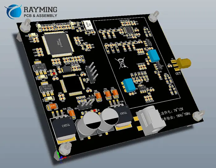
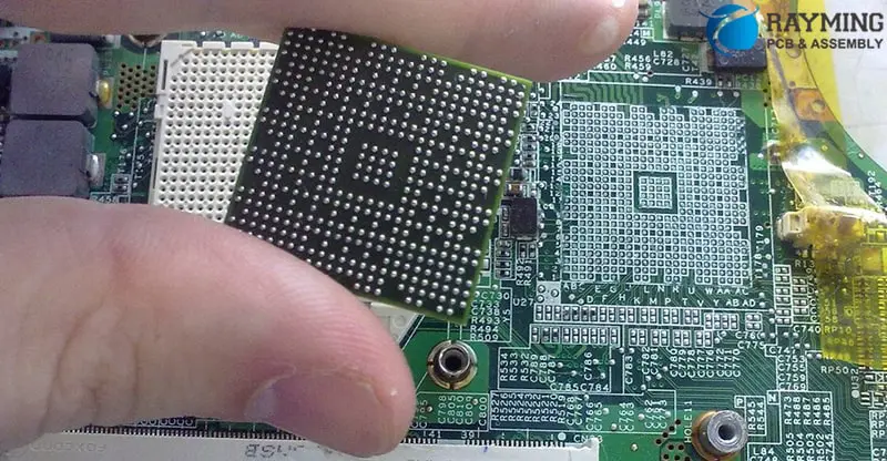
Plenty of circuit processes happen in a specific printed circuit board. It can range from transmission and reception of data, electricity transmission, to communication, etc., based on the type of printed circuit board. Therefore, as a PCB designer or enthusiast, it helps to understand the different PCBs and the PCB relay activities in a circuit. You will not only develop an appropriate PCB for the intended device but ensure that circuit.

https://www.youtube.com/watch?v=T1fNQjelojs

Printed Circuit Board Relays

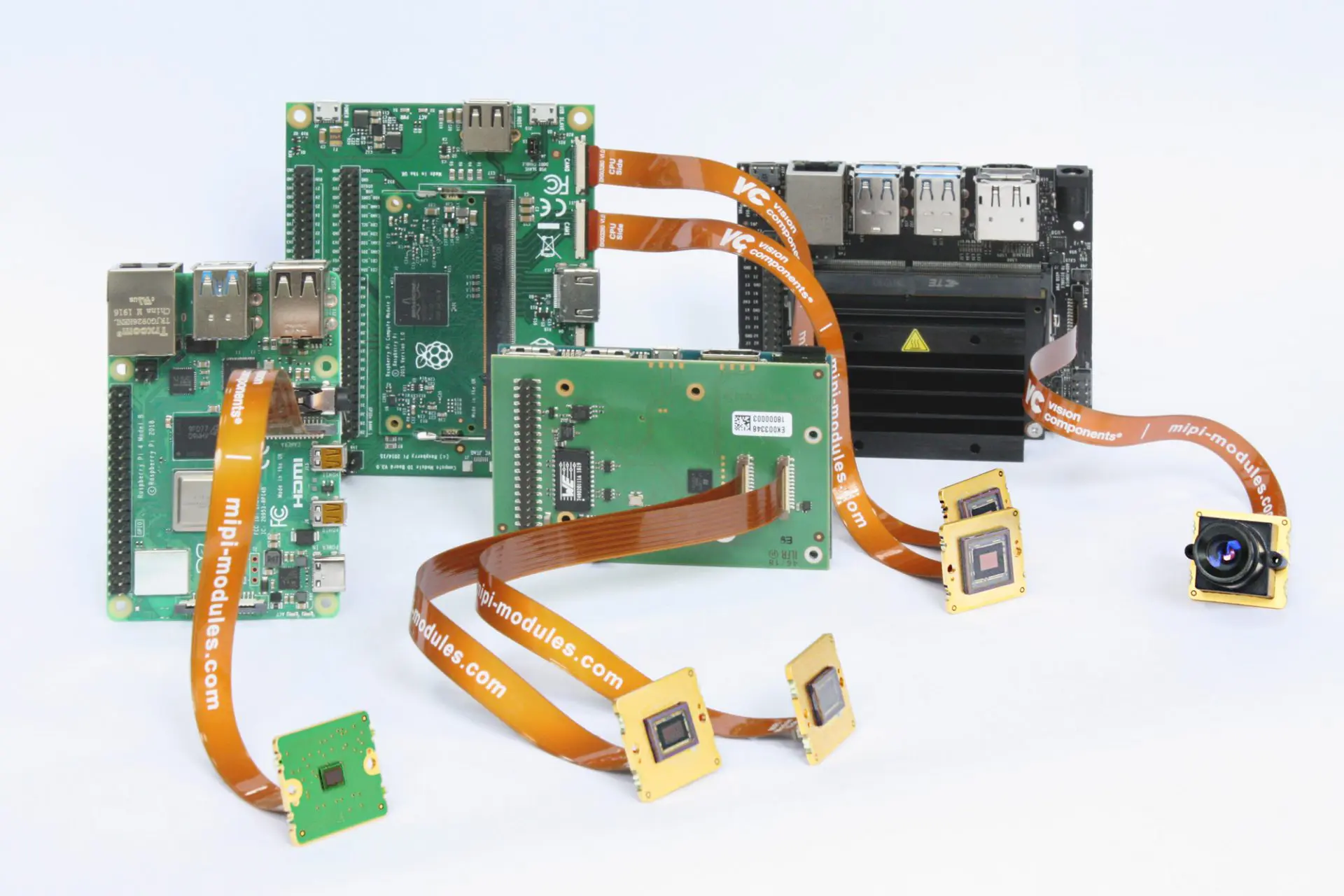
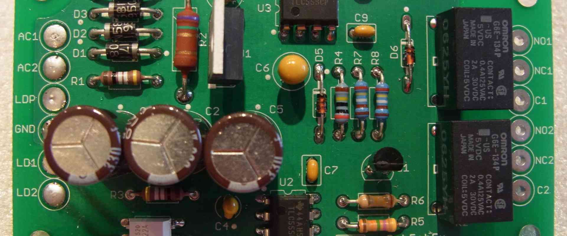
What do you picture with athletics relay activity? Well, relays in circuit boards imply an electrically ran switch, which proves crucial in the proper functioning of PCBs and devices. PCB relay circuits can include a diverse range from reed and electromagnetic to hybrid, thermal, and solid-state relays. A typical DC or AC electromagnetic relay comprises an electromagnet, which receives and converts the electrical signal into the mechanically inclined action of closing and opening the circuit. Besides this, a relay circuit board will typically include an armature, coil, and contacts.

The electromagnetic PCB relay works by applying an electromagnetic field when power gets applied to the coil, subsequently causing the movement of the armature and making the contacts either close or open. PCB relays get classified by construction, mounting type, or function. Consequently, you will get examples of relays such as PCB mount relay, PCB relay 12v, etc.

If you want to buy printed circuit board relays or want to inquire about them, do not look beyond us at RayMing PCB and Assembly Company. You will get incredibly useful information on PCB relays and details on how to order them at a cost-effective price. Further, you can also get information on printed circuit boards.  

Crucial Details about PCB Relays

relay circuit board
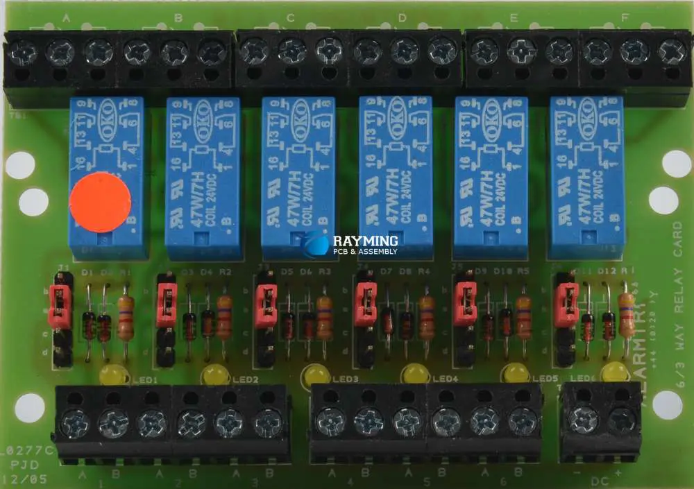
  • Design and components of PCB relay. If you want to make a PCB relay, it becomes vital to remove the relay’s PVC or plastic case using your screwdriver. It will allow you to view the relay parts (spring, armature, coil and contacts, and yoke).  A PCB relay circuit requires the perfect relay and a seamless mounting process to ensure efficient functioning. Because of this, you have to hinge the armature on the yoke and link it mechanically to a single or more moving contact. The relay gets held snugly by a spring, creating an air gap within the magnetic circuit when the relay gets de-energized. Consequently, a set or two of contacts within the relay get closed while the other gets open. However, other relays might have fewer or more contact sets based on their utility.  It also possesses a wire connection between the yoke and the armature, ensuring circuit continuity between the PCBโ€™s moving contacts of the circuit track and armature through the yoke. The relay gets soldered on the printed circuit board.
  • How a relay works
  • As earlier stipulated, the de-energizing of the relay, the magnetic circuit forms an air gap, forcing the two contact sets to close while the other remains open. However, it becomes crucial to note that other relays may have fewer or more contact sets based on their utility. The relay often works through the application of electric current that, when passed through the relay’s coil, generates a magnetic field. It activates the relay’s armature, which breaks or makes a connection with a static contact. Whenever the de-energization of the relay occurs when the contacts are closed, then this movement opens the contacts instead, and the connection breaks. The opposite happens when the situation gets reversed.    

The withdrawal of the current from the coil ensures the return of the armature to its original and relaxed position. While the force that returns the armature gets provided by the spring, gravity also gets applied in instances that involve motor starters of an industrial nature. Most relays by design get manufactured to function fast. In low-voltage applications, it reduces noise, while in high-voltage situations, it limits arcing.

Whenever the coil gets energized with current, it becomes crucial to diode diagonally on the coil. It will dissipate the energy emanating from the disintegrating magnetic field upon deactivation, which would generate a spike in voltage that can hamper the components in the semiconductor.

  • Relayโ€™s pole and throw. Relays operate as switches, and therefore, a similar terminology applies in relays as it does in switches. A relay will switch at least a single-pole, with its contacts getting can getting be-thrown through the energization of the coil. Energization of the coils can happen in one of three ways, which entail the following.
  • NO or Normally-Open contacts complete the circuit whenever the relay gets activated and deactivates when the relay gets disconnected. No has diverse synonyms ranging from “Make” contact, “Early-Make,” or “NOEM.” It all implies the contacts closing before fully engaging the switch or button.  
  • NC or Normally-Closed contacts disengage the circuit upon activation of the relay. Please note that the circuit gets connected if the relay proves inactive. It also gets referred to as “Form B contact” or “Break contact.”
  • CO or Change-Over is also inferred as DT (double-throw). The contact controls the two circuits that feature one having open contact and the other with closed contact.

Below some of the crucial designations encountered.

  • SPST. It denotes a single pole single throw and contains two terminals that can get disconnected or connected. When you include two (accounting for the coil), then the relay possesses four terminals overall. In instances where you encounter an SPNC or an SPNO term, understand that this aims to resolve the ambiguity that arises with the pole’s stature (whether closed or open)
  • SPDT. It denotes the single pole double throw. It has one terminal that connects to two one of the other two. If you include the two that account for the coil, the relay has a total of five terminals.
  • DPST. It denotes a double pole single throw. It has two terminal pairs and equates two of the SPST relay or switches actuated through one coil. If you include the two, accounting for the coil, it possesses a total of six terminals.
  • DPDT. It denotes a double pole double throw and has two change-over terminal rows. It equates to two SPDT relays or switches; all actuated through one coil. It contains eight terminals that include the coil.
  • CO or Change-Over Relay (DT or Double-throw relay)
  • It has close similarities to the SPDT relay. Like SPDT, the configuration switches from a single common pole to the other two and flips between them. For instance, when you consider a relay (SPDT) with a single “C” pole, with the others coming as “B” and “A,” Whenever the coil proves inactive, the “C” gets connected to “A” and in a resting point. However, when the relay gets powered, the “C” gets connected to “B” in a resting point. Therefore, the position only proves one of either resting, with the other needing the coil to get powered.  
  • Relayโ€™s current and voltage position. Plenty of relays get availed in diverse operating voltages such as 5, 6, 12, and 24V. Therefore, if the needed operating voltage gets supplied, the relay gets activated. A relayโ€™s operating voltage typically comes in DC while contractors and main control relays operate with AC coils. A relayโ€™s terminal residuals get used to connecting with DC or AC (50/60Hz) circuits. But take note of the fact that contact pins and switching have maximum current and voltage parameters/ ratings. It always gets in-scripted on the relayโ€™s PVC or plastic case. It becomes essential to restrict yourself within these confines when using the relay. However, you can use a higher current whenever the voltage proves lower. But try and avoid overloading the relay to limit damage and burning out of the appliance or circuit connected. Always endeavor to pick a relay that will handle your current and voltage requirements to avoid incidences of burning out your relay coil.
  • Reuse and recycle old relays. It always proves possible to desolder old or existing circuits before resoldering new circuits as relays cannot get burned with excessive soldering. You can also recycle the coil’s windings, and this includes diverse circuits and jumper wires. In addition, you can reuse the screws and contacts, bolts, nuts, and relay washers.

Mounting Techniques and PCB Design Needs for Electromagnetic Relay

It has become apparent that PCB relays play a significant role in consumer electronics, control panels, scientific and medical equipment. Additionally, by now, you have learned about the different types of PCB relays. But how can you mount a PCB relay on a printed circuit board? A PCB relay only becomes crucial when mounted and functioning on the PCB. To understand this better, we detail the mounting techniques involved in relay circuit boards.

Classification of relays by the mounting technique entails surface mounting and discrete mounting techniques. However, this mounting technique often relies on the board type involved.  

When it comes to the printed circuit board design needs for relays, you need to consider a few fundamental aspects, especially on the mounting technique. For instance, when developing smaller electromagnetic relays that have to get soldered on the printed circuit board, you must consider the physical process needs that might affect the mounting process. Some of these requirements include becoming attentive to the heat application, soldering, and washing. It becomes a problem when the physical processes during the mounting process distort the relayโ€™s internal electromagnetic mechanism. In such an incidence, the relay will underperform when measured against its expected standards.

Conclusion

PCB relays prove a crucial aspect of printed circuit boards, and thus every designer has to understand different aspects of these relays. You cannot design a PCB design without taking into account the PCB relay aspects.

Design and application of PCB Camera

pcb camera module

PCB cameras are a kind of little impression camcorder that are esteemed for their overall flexibility. With optical gadgets and picture sensors mounted straightforwardly on a camera circuit board, manufacturers can forfeit parts to give a space-saving plan. Surveillance systems and cellular phones and are the most conspicuous managers of board cameras.

Camera PCB is computerized cameras with optical recording devices (image sensor, lens, and aperture straightforwardly appended to a printed circuit board with normal I/O. Most camera circuit boards are little in sizeโ€”enlisting only 1/3″ in lens measurement. CCD picture sensors are generally normal; however, CID and CMOS sensors are utilized too. Without a predefined gadget, cameras PCB hold the usefulness of camcorders by and large.

The presentation of a PCB camera is handed off through the input/output of the PCB, regularly a showcase or handheld screen. Since there are no simple controls, one can control the recording alternatives through this interface. Appended to a programmable logic regulator, camera PCB can go about as a kind of vision framework.

PCB Camera Quality

camera PCB

Video Output

Most PCB cameras give a video feed through 75 Ohms composite yield. Yet different choices do exist. With an essential power supply, some PCB cameras can transmit wireless signals. USB and Firewire availability is normal when a memory is associated with the camera circuit board.

Sensitivity

Unmistakable by the nature of the image in low-light circumstances, sensitivity is estimated in lux. Highly contrasting PCB cameras are significantly touchier than their color partners, and some monochrome PCB cameras are fit for recording in conditions with just .0003 lux. It is useful in spy camera circuit board. Colored PCB cameras require more brightening to record a quality picture. The most negligible lux levels for first-class level color PCB cameras will, in general, be .3 lux.

Shutter Speed/Exposure

By utilizing an advanced picture sensor, PCB cameras do not have a screen in the visually appealing film feeling of the word but instead utilize an electronic shutter that guarantees the picture sensor records a unified picture. In pinhole cameras, there is one preassigned exposure rate since the gap cannot be changed. Auto-exposure is regularly used in PCB cameras.

Frame Rate

Frame rates for camera PCBs will, in general, be around 30 edges each secondโ€”the normal frame rate for the TV show. Since PCB cameras compromise on some usefulness to represent their little impression, gadgets fit for recording at more than 100 frames each second are viewed as high velocity. Since PCB cameras are not utilized for movement investigation, this is commonly more than adequate.

Resolution

The goal of PCB cameras is commonly rather poor when contrasted and other bigger cameras. A level goal of 700 TVL is considered extraordinary. While even more decently valued at this point, fit cameras have a resolution between 380โ€”480 TVL.

Lens

Camera lenses have the best impact on the nature of a picture. Due to the small height of PCB cameras, pinhole plans are accessible. PCB cameras likewise use selective lens types.

  • C and CS: These are uncommon mount lenses and TPI strings for mounting. With flange-back distances of 12.5 mm and 17.5 mm individually and widths of one inch, these focal points are select except if there is a connector.
  • Pinhole cameras do not use lenses and are normal for reconnaissance since they can be hard to distinguish. Light goes through the opening onto the picture sensor. More modest openings bring about keener yet dimmer imaging. Touchy CCDs are utilized.
  • Sized camera lenses decide the point of the center for the picture sensor. More modest sizes offer a more extensive point. Normal sizes include 16 mm, 20ยฐ FOV; 6 mm, 53ยฐ FOV; 3.6 mm, 92ยฐ FOV; 2.8 mm, 115ยฐ FOV; 2.1 mm with 150ยฐ FOV.

Specifications

FULL PCB MANUFACTURING Quote

With the direct camera mounting onto the PCB and the little impression of these cameras, mounting alternatives for PCB cameras are boundless. CCTV camera PCB board are put secretly to record ignorant subjects. It includes mirrors, toys, clocks, and other secret camera applications. Camera circuit boards are additionally regularly utilized in computers, tablets, phones, and other mobile gadgets. PCB cameras do not have a typical mounting choice, like sections or stands. They regularly consolidate electromagnetic protection in their lodging. It keeps obstruction from close by electrical segments.

These specifications are regularly discretionary on camcorders, yet they will improve video quality by relying on the utilization.

  • Zoom:ย Cameras are planned with an element that permits the gadget to zero in on far-off objects intently. Optical zooms offer preferred resolution over digital zooms.
  • Progressive Scan:ย It is a CCD plan that permits procurement of both even and odd fields simultaneously. Every pixel contains data from one complete frame. This innovation permits high resolution without the utilization of an automatic color. Reformist output cameras are utilized for picture procurement of quickly moving articles and exact dimensional estimations.
  • Outdoor Rated:ย Outdoor-evaluated gadgets are intended to withstand outside temperature varieties, downpours, snow, and other climate conditions.
  • Machine Vision Sensors:ย They can break down occasions caught by its camera and ready administrators or settle on choices dependent on the data gathered. These are likewise called smart cameras. If they are not uniform machines, the camera is ordinarily connected to a PC interface through an Ethernet, USB, or FireWire.
  • Low-Light Camera:ย These are intended to be utilized in dim circumstances where a generally reasonable camera will not arrive at an openness level equipped for catching a picture. The cameras contain picture sensors that are uncommonly insightful of discreet light sources.
  • High Definition:ย It is a video standard with higher picture sharpness, bigger picture, more tones, and better solid than ordinary video guidelines. PCB cameras are not generally equipped for genuine HD video, the meaning of 1,280 x 720 pixels.
  • Gamma Correction:ย Gamma is the nonlinear connection between the video signal level and the resulting picture component brilliance. Gamma rectification makes up for this nonlinearity to deliver the picture valid in color while at the same time giving power to the first item.
  • Gain Control:ย It utilizes electronic hardware to build video signals in low-light conditions. It can present noise and, along these lines, graininess in the image. Typically, AGC is handicapped, and particulars are given this element killed.
  • Dome:ย Cameras are encased in a defensive arch produced using materials like acrylic or polycarbonate. Typically, these materials are optically remedied for special picture catch. It can make a sealed lodging normal for security use.
  • Auto-Lens:ย The activity is when the lens iris naturally changes to keep a foreordained degree of light on the picture pickup gadget. Cameras with auto-lens mode may likewise give autofocusing.
  • Anti-Blooming:ย Saturation happens when the light that is detected surpasses a pixel’s ability to transmit electrons. An unreasonable charge can seep into neighboring pixels and cause splendid spots or streaks to show up on the picture. A condition referred to as blooming. Against blooming, entryways eliminate unreasonable charges and can fundamentally decrease blooming, yet regularly at the expense of diminished affectability.

Applications

While CMOS and CCD, and chips are utilized in mobile phones and digital cameras, they have different applications. Phones are by a long shot the greatest concentration of CMOS makers. A gigantic measure of cash, examination, and improvement has gone into making the best yet littlest CMOS imager, so the chips occupy next to no room. The most recent consequence of this exploration is Google Glass, a generally new gadget made by Google that incorporates a great little camera that sits on a couple of glasses. This camera is so lightweight that the vast majority do not feel it by any stretch of the imagination.

Notwithstanding digital cameras, CMOS and CCD chips can likewise be found in camcorders. CMOS chips are exceptionally mainstream on account of how modest they are and how the pictures taken by some CCTV PCB board do not need to be unimaginably pointed by point. Before video observation, the film was frequently clear, for instance, and the resolution was not in every case unbelievably high since organizations needed to store many recordings. The security business has accepted CMOS sensors principally due to their minimal expense and capacity to coordinate these imagers in spy camera circuit boards effectively.

CCD sensors, in any case, do have their employments. Since they are so delicate to light, CCD picture sensors are utilized by cosmologists in a wide range of satellites and other space cameras. Perhaps the most acclaimed, the Hubble Space Telescope, utilizes a CCD exhibit to catch a wide range of flawless pictures it has assumed control throughout the long term. CCD chips are likewise found in spectrometers and various scientific instruments utilized in space science.

We use CMOS in radio-recurrence coordinated circuits found in different remote gadgets and in gadgets that utilize microwave frequencies. We can also utilize CMOS picture chips in various spots. For example, utilizing it in an inconsistent message and transmission doors.

Conclusion

Since both CCD and CMOS have various applications, it isn’t easy to settle on a positive choice on which is better. It relies upon what the gadget is being utilized for. While CMOS chips are less expensive and will presumably turn into the standard for practically consistent gadgets with cameras, they may never supplant CCD contributes to some regions because of the special way CCD chips work. CMOS chips would never be utilized in particular gadgets just because they work uniquely.

Since the picture nature of CMOS sensor camera frameworks is turning out to be better a lot, it is anything but’s a brief time frame before CMOS replaces CCD sensors. Since various expert photographers can access and use CCD cameras, there is no uncertainty that CMOS cameras are a wide margin the more mainstream of the two. The minimal expense of CMOS picture chips and how they can be produced with no exceptional hardware makes them ideal for use in digital cameras and cell phones focused on the overall population. Because of their sensitivity to light, CCD picture sensors may keep on being utilized in specific spaces, including Astrophotography.

What are the different types of connectors for PCB?

pcb connector

Introduction

Printed circuit board (PCB) connectors allow detachably joining a board to mating connectors or cables carrying power, signals, or data. The wide variety of PCB connector types suit different applications, environments, circuit types, and design requirements.

This article explores common categories of PCB connectors and interfaces. Weโ€™ll examine board-mount connector characteristics, orientations, mounting styles, electrical properties, signal classes, and usage scenarios. Understanding PCB connector selection principles enables choosing the optimal solutions for electronics projects and products.

Connector Functionality

PCB connectors facilitate:

  • Board-to-wire connections โ€“ Interface between PCB and external cables or harness.
  • Board-to-board โ€“ Stacking PCBs electrically end-to-end or side-by-side.
  • Board-to-panel โ€“ Mounting PCBs flush into racks, chassis, or enclosures.
  • I/O interfaces โ€“ Connectors for external controls, peripherals, or instruments.
  • High-speed data โ€“ Transmitting fast digital data streams.
  • Power input โ€“ Delivering supply power into the PCB.

Matching connector functionality to the need is the first criterion.

Electrical Interface Types

pcb-connectors-wire-to-board

Common PCB connector interface technologies include:

Analog/Power

  • General purpose โ€“ Discrete wires for low frequency analog signals or power transmission.
  • Coaxial โ€“ Shielded signal line plus ground return. For high frequency analog.

Digital Data

  • Rectangular multipin โ€“ Parallel row of pins. For ribbon cables or IDC motherboard sockets.
  • D-subminiature โ€“ Compact density DB connectors. RS-232 serial ports.
  • RJ45 โ€“ Ethernet and datacom modular jacks for unshielded twisted pair cable.

High-Speed Digital

  • USB โ€“ For connecting peripherals with the ubiquitous USB standard.
  • PCI Express โ€“ Advanced PCIe data bus for boards or external devices.
  • SFP โ€“ Pluggable gigabit fiber optic transceivers.

Storage

  • SATA โ€“ Serial bus widely used in computer disk drive connections.
  • M.2 โ€“ Compact SSD card edge connector.

Specialty

  • Board stack โ€“ Stacking interconnect for mezzanine PCBs. High density vertical mounting.
  • FFC/FPC โ€“ Flexible printed circuit connections from flat flex cables.

The required signal classes steer interface selection.

Connector Mounting Styles

Connectors attach to PCBs through:

Through-Hole Mounting

  • Leads pass through holes in PCB.
  • Requires board drilling.
  • Robust mechanical attachment.

Surface Mounting

  • Leads directly solder to pads on surface.
  • Conserves board space.
  • Reflow solder attachment.

Press-fit

  • Pins press into plated through-holes.
  • Gas-tight interference fit.
  • No soldering.

SMT Sockets

Edge Board Sockets

  • Connect fingers grip PCB edge.
  • Common for plug-in cards.

Mounting suits manufacturing constraints and connectors.

PCB Connector Orientations

Connectors attach to boards in different orientations:

Vertical Mount

  • Exit board perpendicular (most common).

Right-Angle

  • Exit board parallel in 90ยฐ bend.

Horizontal Mount

  • Attaches flat to board surface.

Mezzanine Stacking

  • Directly interconnects multiple parallel boards.

Front Mount

  • Mounts to edge of board.
  • Common for external instrument connections.

Orientation depends on design form factor and space requirements.

Common Types of PCB Connectors

hdmi-pcb-connector

Some of the most prevalent types of connectors used with PCBs include:

Header Connectors

  • Vertical insulating housings holding pin or socket contacts.
  • Friction-lock with mating socket strip or plug.
  • Standard 0.1โ€ pitch. Good for general I/O connections.

D-Sub Connectors

  • Rectangular shell with arrayed crimp pin contacts.
  • Secures with screws to mate with socket.
  • Used for composite video, VGA, serial ports.

RJ45 Connectors

  • 8P8C modular connectors for Ethernet and datacom.
  • Tab-down vertical SMT footprint.
  • Can have integrated magnetics.

USB Connectors

  • Type A, type B, micro AB, and USB-C options.
  • SMT and through-hole versions available.

Board Stacks

  • Direct board-to-board interface.
  • High density with mm pitch.
  • Samtec, TE, Amphenol manufacturers.

FFC/FPC Connectors

  • Mechanical clamping or ZIF sockets for flex cables.
  • Low profile, pitch under 1 mm.

There are many other speciality connector varieties beyond this sampling.

Key Connector Specifications

Technical factors drive connector selection for fit and performance:

  • Pitch โ€“ Centerline spacing between contacts. From 2.54 mm to under 1 mm.
  • Current/Voltage โ€“ Current capacity and working voltage per contact.
  • Interface โ€“ Type of signal lines needed. E.g. LVDS pairs.
  • Speed โ€“ Maximum frequency. Important for protocols like PCIe, USB.
  • Mating cycles โ€“ Lifetime durability rating.
  • Contact type โ€“ Material and plating. Gold preferred for corrosion resistance.
  • Temperature range
  • Polarization โ€“ Keying to ensure mating alignment.
  • Springs โ€“ Contact normal force and deflection range.
  • Termination โ€“ Solder, press-fit, other PCB mounting styles.
  • Size โ€“ Available PCB real estate and keep out regions.

Designing Connectors into PCBs

Best practices for integrating connectors in PCB design:

Schematics

  • Abstract connectors into neatly labeled functional blocks rather than individual pins.

Layout

  • Group related connectors together when possible.
  • Ensure adequate clearance space for mating plugs.
  • Use polarizing cutouts to prevent mis-plugging.

Cabling

  • Plan cable bend radius exiting board.
  • Support cables appropriately in enclosure.

Modeling

  • Include connectors in electromagnetic simulations of PCB.

Testing

  • Inspect for proper seating, alignment, and retention in prototypes.

Getting connectors designed-in robustly avoids issues and rework.

Selecting Connectors

Tips for choosing the optimal connectors:

  • Match specifications to electrical, mechanical, environmental needs.
  • Consider ease of assembly into production processes.
  • Test samples to validate usability and performance.
  • Review options from multiple vendors for alternatives.
  • Leverage existing designs with proven connectors when possible.
  • Seek expert guidance from component vendors.

Taking care selecting suitable connectors prevents problems arising in the field.

Conclusion

The wide variety of PCB connector types and mounting configurations allows designers to interface their electronics in the optimal way for the product and manufacturing requirements. Whether using standard interfaces like USB, press-fit pins, or direct board stacking, connectors bridge the gaps between PCBs and the outside world. Carefully considering electrical, mechanical, and assembly factors leads to robust connector integration that performs reliably throughout the product lifetime.

Frequently Asked Questions

What are considerations for connectors used in high vibration environments?

Using positive retention like screws or clips, preventing looseness in mated connectors, employing board locks, selecting ruggedized interconnections, and applying conformal coating help connectors withstand vibration.

How are high pin count connectors effectively routed on PCBs?

Using wider trace escape routing, pin grouping into bussed nets, reference planes for controlled impedance, and termination resistors help manage routing complexity for large connectors.

What are considerations for PCB connectors used in harsh environments?

Using sealed, liquid-tight connectors, avoiding dust-trapping crevices, specifying watertight board feedthroughs, considering contact plating like gold, and mechanical strain relief help connectors survive difficult environments.

How can you determine the right current rating for a power connector?

Calculate the maximum steady state and peak supply current for the PCB, consider derating and margins, and select connector current capacity above the power needs.

What are techniques to improve EMI shielding around connectors?

Using metal connector shells grounded to chassis, picking connectors with integrated shielding, surrounding connectors with plated guard traces, backside ground plane tying, and flexible contact finger gaskets help reduce emissions and ingress through connectors.

The Top 10 Design Rules for Digital PCB

digital pcb

Digital PCB technology has made significant strides in the field of electronics, driven by the growing demand for faster, smaller, and more affordable electronic devices and gadgets. These advancements have led to the development of digital PCBs, which incorporate multiple microprocessors and electronic circuitry capable of handling thousands of operations per second. Compared to analog circuit boards, digital PCBs offer several key improvements, including superior impedance matching and enhanced control over insertion loss in transmission lines.

The design and engineering of digital PCBs require meticulous attention to detail to address potential issues such as impedance discontinuities in transmission lines, inadequate plating of through-hole interconnections, and other signal integrity challenges. Digital PCBs possess several distinctive features that make them highly effective in electronic circuit applications. These features include:

  • High layer count
  • Tight dimensional tolerances
  • Stub elimination
  • High packaging density
  • Complex stack-up structure

These attributes collectively contribute to the superior performance and reliability of digital PCBs in modern electronic systems.

1. Proper Component Placement

One of the foundational aspects of PCB design is the strategic placement of components. This rule is especially critical for digital PCBs, where signal integrity and power distribution are paramount.

Why It Matters

Proper component placement can:

  • Reduce signal path lengths
  • Minimize electromagnetic interference (EMI)
  • Improve thermal management
  • Enhance overall circuit performance

Best Practices

  • Group related components together (e.g., keep microcontrollers close to their supporting components)
  • Place high-frequency components near the board edge to minimize interference
  • Consider the direction of signal flow when arranging components
  • Keep sensitive analog components away from noisy digital circuits
  • Ensure adequate spacing between components for ease of assembly and rework

By adhering to these placement guidelines, you’ll create a more efficient layout that not only performs better but is also easier to manufacture and maintain.

2. Optimal Power Distribution

In digital PCBs, clean and stable power distribution is crucial for ensuring reliable operation of all components.

Why It Matters

Proper power distribution:

  • Reduces noise in the power supply
  • Prevents voltage drops across the board
  • Ensures all components receive adequate power
  • Minimizes the risk of electromagnetic interference

Best Practices

  • Use power planes instead of traces for main power distribution
  • Implement a star topology for power distribution when possible
  • Place decoupling capacitors close to the power pins of ICs
  • Use wide traces or polygons for high-current paths
  • Consider using multiple smaller vias instead of one large via for better current distribution

By focusing on optimal power distribution, you’ll create a more stable operating environment for your digital components, leading to improved performance and reliability.

3. Signal Integrity Considerations

Maintain the shortest SDRAM signal return path

Signal integrity is a critical aspect of digital PCB design, especially as clock speeds and data rates continue to increase.

Why It Matters

Good signal integrity:

  • Ensures accurate data transmission
  • Reduces errors and glitches in digital circuits
  • Minimizes crosstalk between signal lines
  • Improves overall system reliability

Best Practices

  • Keep high-speed signals short and direct
  • Use differential pairs for high-speed signals when possible
  • Maintain consistent trace widths for matched impedance
  • Avoid 90-degree angles in traces; use 45-degree angles or arcs instead
  • Use ground planes and proper stackup design to control impedance
  • Implement termination techniques for long signal lines

By prioritizing signal integrity in your design, you’ll create a PCB that can handle high-speed digital signals with minimal distortion and interference.

4. Proper Stackup Design

The PCB stackup refers to the arrangement of copper and dielectric layers in a multi-layer board. A well-designed stackup is crucial for digital PCBs.

Why It Matters

An optimized stackup:

  • Improves signal integrity
  • Enhances power distribution
  • Reduces EMI/EMC issues
  • Provides better control over impedance

Best Practices

  • Use an even number of layers for better symmetry
  • Alternate signal and ground/power layers
  • Keep high-speed signals on layers adjacent to ground planes
  • Use thicker dielectrics between power and ground planes to increase capacitance
  • Consider using buried vias for dense designs

By carefully designing your PCB stackup, you’ll create a more robust foundation for your digital circuits, leading to improved performance and reduced electromagnetic issues.

5. Effective Grounding Techniques

Proper grounding is essential in digital PCB design to ensure signal integrity and minimize noise.

Why It Matters

Effective grounding:

  • Provides a low-impedance return path for signals
  • Reduces ground bounce and noise
  • Improves EMI/EMC performance
  • Enhances overall circuit stability

Best Practices

  • Use a solid ground plane whenever possible
  • Implement a single-point grounding strategy for mixed-signal designs
  • Avoid creating ground loops
  • Use multiple vias to connect ground planes between layers
  • Keep ground return paths as short as possible

By implementing effective grounding techniques, you’ll create a more stable and noise-resistant environment for your digital circuits.

6. Clock Signal Routing

The high and low versions are not part-time

Clock signals are critical in digital PCBs and require special attention during the routing process.

Why It Matters

Proper clock routing:

  • Minimizes clock skew
  • Reduces EMI
  • Ensures synchronous operation of digital components
  • Improves overall system timing

Best Practices

  • Keep clock traces as short as possible
  • Use controlled impedance routing for clock signals
  • Avoid routing clock signals near sensitive analog circuits
  • Implement proper termination for clock lines
  • Consider using a clock distribution network for complex designs

By carefully routing your clock signals, you’ll ensure that your digital circuits operate in sync and with minimal interference.

7. Decoupling and Bypass Capacitors

Decoupling and bypass capacitors play a crucial role in maintaining stable power supply voltages and reducing noise in digital circuits.

Why It Matters

Proper use of decoupling capacitors:

  • Reduces power supply noise
  • Improves signal integrity
  • Minimizes EMI
  • Enhances overall circuit stability

Best Practices

  • Place decoupling capacitors as close as possible to IC power pins
  • Use a combination of different capacitor values for broadband noise suppression
  • Consider using array capacitors for high-density designs
  • Implement a PDN (Power Distribution Network) analysis to optimize capacitor placement
  • Use low-ESR (Equivalent Series Resistance) capacitors for high-frequency applications

By implementing effective decoupling strategies, you’ll create a more stable power environment for your digital components, leading to improved performance and reliability.

8. Thermal Management Considerations

As digital circuits become more complex and compact, thermal management becomes increasingly important in PCB design.

Why It Matters

Effective thermal management:

  • Prevents component overheating
  • Improves reliability and longevity of the PCB
  • Ensures consistent performance across temperature ranges
  • Reduces the risk of thermal-induced failures

Best Practices

  • Use thermal vias to dissipate heat from critical components
  • Implement copper pours for better heat distribution
  • Consider using heat sinks for high-power components
  • Place heat-generating components away from temperature-sensitive parts
  • Perform thermal simulations to identify potential hotspots

By addressing thermal concerns in your PCB design, you’ll create a more reliable and long-lasting product that can withstand various operating conditions.

9. EMI/EMC Design Considerations

Electromagnetic Interference (EMI) and Electromagnetic Compatibility (EMC) are critical factors in digital PCB design, especially as circuits operate at higher frequencies.

Why It Matters

Proper EMI/EMC design:

  • Ensures compliance with regulatory standards
  • Reduces interference between components and systems
  • Improves overall product reliability
  • Minimizes the risk of signal integrity issues

Best Practices

  • Use proper shielding techniques for sensitive circuits
  • Implement EMI suppression components (e.g., ferrite beads, common-mode chokes)
  • Design with EMC-aware component placement and routing
  • Consider using spread spectrum techniques for clock signals
  • Perform pre-compliance EMC testing during the design phase

By incorporating EMI/EMC considerations into your digital PCB design, you’ll create a product that not only performs well but also meets regulatory requirements and operates reliably in various environments.

10. Design for Manufacturing (DFM) and Testing

While focusing on electrical performance is crucial, it’s equally important to design your digital PCB with manufacturing and testing in mind.

Why It Matters

Designing for manufacturing and testing:

  • Reduces production costs
  • Improves yield rates
  • Facilitates easier assembly and rework
  • Enables more effective testing and quality control

Best Practices

  • Follow manufacturer guidelines for minimum trace widths, spacings, and hole sizes
  • Include fiducial markers for automated assembly
  • Design for panelization to improve manufacturing efficiency
  • Implement test points for critical signals
  • Consider using boundary scan (JTAG) for complex digital designs
  • Include silkscreen markings for component orientation and identification

By incorporating DFM and testing considerations into your digital PCB design, you’ll create a product that is not only high-performing but also cost-effective to manufacture and easy to test and maintain.

Conclusion

Mastering the top 10 design rules for digital PCBs is essential for creating high-performance, reliable, and manufacturable electronic products. From proper component placement and power distribution to signal integrity and thermal management, each aspect plays a crucial role in the overall success of your PCB design.

Remember that these rules are not isolated concepts but interconnected principles that work together to create a holistic design approach. As you gain experience and tackle more complex projects, you’ll find that balancing these various factors becomes an art as much as a science.

Stay up-to-date with the latest industry standards and best practices, as PCB design is an ever-evolving field. Utilize advanced design tools and simulation software to validate your designs before production. And most importantly, never stop learning and experimenting โ€“ the world of digital PCB design is full of challenges and opportunities for innovation.

By following these top 10 design rules and continually refining your skills, you’ll be well-equipped to create cutting-edge digital PCBs that meet the demands of today’s fast-paced electronic industry. Whether you’re working on consumer electronics, industrial equipment, or advanced computing systems, these principles will serve as a solid foundation for your PCB design journey.

How to Design Audio PCB Circuit Board?

Audio PCB

Introduction

Printed circuit boards designed for audio applications require careful engineering to deliver quality sound performance. Audio PCBs need controlled impedances, shielding, filtering, and tight layout to maintain signal integrity.

This article provides guidance on best practices for designing analog audio PCBs, from amplifier circuits to audio codecs and digital interfaces. Weโ€™ll review layout considerations, component selection, routing techniques, and design methodologies tailored for audio. Letโ€™s explore how to design clear, robust, and interference-free audio PCBs.

Audio Frequency Ranges

The first step is understanding the frequency ranges involved in various audio applications:

  • Human hearing – Approx 20 Hz to 20 kHz max frequency range. Defines analog audio.
  • Voice bandwidth – 100 Hz to 7 kHz containing most speech information.
  • Hi-fi audio – High fidelity reproduction targeting 20 Hz – 20 kHz with low distortion.
  • Digital audio sample rates – 44.1 kHz, 48 kHz, 96 kHz etc based on sampling theory limits.
  • Control/status signals – Digital control bus speeds like I2C, SPI in the 1 MHz range.

Matching the circuit performance to the application’s frequency range is crucial.

Key Design Considerations for Audio PCBs

Audio Components

To achieve good signal integrity, audio PCB layouts must address:

  • Impedance control – Matched 100ฮฉ differential impedance typical.
  • Low noise – Avoid crosstalk, digital interference, ground loops.
  • Filtering – Low pass filter digital signals.
  • Power conditioning – Clean, regulated, ripple-free power.
  • Component selection – High quality capacitors, op amps, ADCs, etc.
  • Grounding – Well designed grounding minimizes noise injection.
  • Shielding – Isolate analog signals from interference sources.
  • Board stackup – Well designed layer stack and component placement.

Paying attention in these areas ensures clarity and accuracy of the audio signal.

Audio Amplifier Circuit Design

Audio amplifiers boost microphone, instrument, or line level signals to drive speakers or recording equipment. Here are key amplifier PCB design considerations:

Gain Stages

  • Cascaded gain stages provide required overall amplification.
  • Typically 3-5 stages for heavy amplification.
  • Can combine transistor and op amp stages.

Biasing

  • DC biasing sets proper operating points for amplification.
  • Combine resistors, feedback loops, and other bias techniques.

Feedback and Compensation

  • Feedback provides impedance bridging, gain control, and compensation.
  • Ensures stability for all expected circuit conditions.

Power Supply Filtering/Bypassing

  • Clean steady DC supply prevents noise injection.
  • metic filters, regulated design, proper decoupling.

Heat Dissipation

  • Adequate cooling for heat generating components.
  • Thermal design, copper fills, board mountings.

Careful analog design results in low noise and distortion.

Audio Codec, DAC, and ADC Circuits

Digital audio codecs, ADCs, and DACs translate audio signals between the analog and digital domains:

Component Selection

  • High performance audio-grade converters, amplifiers, and clocks.
  • Review specs like SNR, distortion, dynamic range.

Impedance Matching

  • Ensure proper impedance bridging at interfaces.
  • line driver amps, feedback networks.

Sampling Rate Support

  • Handle typical rates like 44.1 kHz up to 192 kHz.
  • Use oversampling DACs/ADCs if needed.

Filtering

  • Anti-aliasing and reconstruction filters for clarity.
  • MEMS microphone tuning and protection.

Port Isolation

  • Separate sensitive analog and noisy digital domains.
  • Digital/analog power plane splits.

Meticulous design maximizes audio resolution and dynamic range.

Digital Audio and Control Interface Design

Digital audio and control bus signal integrity also matters:

Signal Termination

Interface Layout

  • Keep lines short, avoid 90ยฐ angles.
  • Solid ground references.
  • No noisy signals routed parallel.

Board Stackup

  • Route fast digital traces on inner layers.
  • Reference to unbroken ground planes.

Power Decoupling

  • Proper decoupling near digital ICs.
  • Filter power supply inputs.
  • Separate analog and digital supplies.

Care with digital interfaces prevents noise coupling into sensitive analog circuits.

Component Selection for Audio Boards

Thoughtful part selection is crucial for audio PCBs:

Audio ICs

  • High quality amplifiers, codecs, converters.
  • Low noise, low distortion, low crosstalk.

Passives

  • 1% or better resistors, tight tolerance caps.
  • Low ESR/ESL, stable temperature coefficients.

Connectors

  • Gold plated contacts avoid corrosion.
  • Proper pinouts.
  • Secure connections.

Crystals and Clocks

  • Use audio grade clock sources with low jitter.
  • Ensure caps are nearby for supply filtering.

Even small component choices impact overall sound quality.

Audio PCB Layout Considerations

PCB Antenna Layout

Paying attention to layout is vital for audio boards:

Partitioning

  • Group relevant circuits together.
  • Delineate separate analog and digital areas.
  • Enclose sensitive analog in guards.

Impedance Control

  • Tune trace geometry for target impedance.
  • Reference plane layers help.

Component Placement

  • Place components for short, direct connections.
  • Watch for cross-talk hot spots.

Routing

  • Avoid sharp corners or twisting routes.
  • Use curved traces between sections.
  • Keep out from ground planes.

Every layout choice affects signal integrity – tune carefully.

Shielding and Layer Stackup

Proper board layer stackup and shielding prevents interference:

Layer Usage

  • Analog signals inner layers.
  • Digital signals outer layers or internal power plane adjacent.
  • Split power planes between analog and digital domains.

Shielding

  • Use copper fills around sensitive areas.
  • Careful stitching vias to connect shields.
  • Spot shields around digital ICs.

Enclosure Shielding

  • Seamlessly connect board shields to chassis ground.
  • Prevent leakage through openings.

Shielding is the cornerstone of noise mitigation.

Audio PCB Design Process

A structured design process ensures good results:

  1. Define requirements – frequency range, dynamic range, distortion limits.
  2. Create schematic for amplifiers, converters, processors.
  3. Select components for low noise, high linearity.
  4. Develop board stackup and partition sections.
  5. Floorplan components and route critical connections.
  6. Route thoroughly, tuning impedances and shielding.
  7. Perform signal, power integrity, and EMI analysis.
  8. Review design rules and adjust layout as needed.
  9. Iterate until all specifications are met.
  10. Validate with thorough bench testing.

Care at each stage leads to a successful audio PCB implementation.

Conclusion

Designing audio PCBs requires care and expertise to maintain signal integrity and achieve high analog fidelity. Following best practices for schematic design, simulation, layout techniques, shielding, and frequency management results in boards with excellent acoustic performance. Audio circuits demand meticulous engineering and board implementation to minimize noise, interference, and distortion. A well-executed audio PCB design delivers pristine rendered sound across the entire audible spectrum.

Frequently Asked Questions

What are some typical specifications used to evaluate audio PCB performance?

Key parameters are frequency response, total harmonic distortion (THD), signal-to-noise ratio (SNR), crosstalk between channels, dynamic range, and stability across operating conditions.

What are some simple ways to start improving audio circuit layouts?

Using a clean ground plane, proper decoupling near ICs, separating noisy digital circuits from analog, keeping high speed traces short, using shielding, and minimizing crosstalk hotspots.

Why are maintaining controlled impedances important for audio PCBs?

Controlled impedances like 100ฮฉ differential for clock and audio signal traces prevent signal quality degradation due to reflections and standing waves that cause ringing and distortion.

How can I check an audio PCB design for susceptibility to EMI issues?

Performing appropriate susceptibility simulations, scanning near field probes across the operating board, or testing in a semi-anechoic chamber can reveal emitted or received EMI/RFI issues. Shielding and filtering can then help mitigate observed problems.

What are some audio-specific integrated circuits used in audio PCB design?

High performance audio amplifiers, audio codecs for A/D and D/A conversion, digital signal processors and effects chips, microphone preamplifiers, high resolution ADCs/DACs, and audio-specific microcontrollers.

For printed circuit board design engineers, phones give a definitive test. Every subsystem has conflicting necessities, and current phones incorporate virtually every subsystem found in a compact gadget. An excellent audio PCB must amplify the exhibition of every gadget connected with it and keep the different subsystems from meddling with one another. The conflicting necessities of every subsystem bring about some trade-off. At last, even though the importance of audio in mobile phones is expanding, the audio circuit board is regularly given minimal thought during its pcb layout.

YouTube video

Segment Placement

The initial step of any audio PCB configuration is picking where to put the parts. Careful segment position can ease ground partitioning and signal routing. It limits noise pickup and the audio circuit board required.

The RF part of a phone is regularly viewed as simple. However, there is a typical issue in numerous mobile phone plans where noise coupled from the RF segment into the sound hardware is demodulated into discernible noise. To forestall this, the RF and sound segments should be isolated, however much as could reasonably be expected.

PDAs contain a combination of analog and digital hardware that should be isolated to keep noise from the computerized parcel from meddling with the delicate, simple circuits. Apportioning the audio PCB into an analog and a digital area improves the partition task.

When the audio PCB has been parceled into RF, digital and analog regions, the part arrangement inside the simple segment should be chosen. Segments ought to be set to limit the distance that sound signs travel. Find the amplifier circuit board near the loudspeaker and headphone jack. This placement will limit EMI radiation from Class D speaker enhancers and limit the noise defenselessness of low-sufficiency earphone signals. Put the gadgets providing the simple sound near the enhancer as conceivable to limit noise pickup on the intensifier inputs. All information signal follows will go about as antennas to RF signals. However, reducing the traces decreases the radio wire productivity for frequencies regularly of concern.

Audio circuit board Design Tips

audio circuit board

Designing audio PCB stays a test, and parts of it usually are thought about somewhat of a professional. Indeed, even the best creators frequently need to assemble more than a circuit board to deliver a tremendous noise-free plan. The following are a few hints from our encounters:

OpAmp Circuits

Fast OpAmps are not helpful for sound. There are several issues with gadgets like the LMV722, a 10MHz OpAmp wavering fiercely when utilized with computerized pots that add a touch of propagation deferral to the criticism resistorโ€”changing to an LMV358 which is a 1MHz OpAmp address the issue.

When planning an op amplifier circuit board, you frequently discover you need to alter a sound signal to accomplish the least complicated circuit. It is fine and is just an issue where you have one signal rearranged and another not as this would make them be out of the stage when heard.

Capacitors

Sound sign series capacitors: –

You can use them anywhere if you want to segregate segments from one another. Qualities to utilize: – 100nF is fine 220nF is typical if you need to lessen cost/size, best not to go beneath 100nF.

Try not to utilize ceramic/clay capacitors. The explanation is that fired capacitors will give a piezoelectric impact to an AC signal which causes noise. Utilize a Poly of some kind โ€“ Polypropylene is best; however, any will do. It is reasonable for high purity applications, not a general standard sound plan.

Try not to utilize tantalum capacitors anyplace inside sound sign ways (a few originators may differ; however, they can cause ghastly issues). A by and largely acknowledged substitute for polycarbonate is PPS (Polyphenylene Sulfide).

Interfacing

When interfacing with other hardware, if controlling some different PCBs that incorporate sound hardware guarantee, there is just one point where GND associates between the two boards ought to in a perfect world be at the sound simple sign association point. Would you control the other board utilizing a gliding supply and connect GND without supply power through it? To signal IO associations with different gadgets or to the rest of the world, it is a decent idea to utilize a 100R resistor between GND circuits and the rest of the world GND for everything to stop ground circles made.

Signal

Where conceivable, stay away from in and out the sound signal to and from IC‘s running in equal on the PCB as this can cause motions, which feed on output to input. Keep in mind that simply 5mV can cause a lot of noise. Keep digital ground planes from sound GND and sound hardware by and large. Noise can be brought into sound just from tracks being too close to advanced planes.

Grounding

Grounding is essential in deciding if the framework accomplishes the gadget’s latent capacity. An inadequately grounded framework will probably have high RF susceptibility, crosstalk, noise, and distortion. Albeit one can address how long ought to be committed to framework grounding, a painstakingly planned establishing plan keeps several issues from happening.

The ground in any framework should fill two needs. To start with, it is the return way for all flows streaming to a gadget. Second, it is the reference voltage for both analog and digital circuits. Grounding would be a straightforward exercise if the voltage at all marks of the ground could be similar. All traces and wires have a limited obstruction. It implies that there will be a relating voltage drop at whatever point there is current moving through the ground. Any circle of wire additionally frames an inductor. It implies that at whatever point current streams from the battery to a heap and back to the battery, the current way has some inductance. The inductance builds the ground impedance at high frequencies.

While planning the best ground framework for a specific application is no basic assignment, some broad rules do make a difference to all frameworks.

  1. Flood All Unused PCB Area with Ground: At whatever point two bits of copper run close to one another, a little capacitive coupling is shaped between them. By running ground flood close signal traces, undesirable high-recurrence energy in the sign lines can be shunted to the ground through the capacitive coupling.
  2. Maximize the Effectiveness of Bypass Capacitors: Virtually all gadgets require to sidestep capacitors to give immediate current. Find these capacitors as close as conceivable to the inventory pin, which they are bypassing if you want to reduce the capacitor inductance. Any inductance diminishes the viability of the detour capacitor. Likewise, the capacitor should be given a low-impedance association with the ground to limit the capacitor’s high-recurrence impedance. Straightforwardly interface the ground side of the capacitor to the ground plane instead of directing it as anything but a trace.
  3. Use the Star Grounding Technique for Analog Circuits: Star grounding utilizes a solitary point on the PCB as the main ground point. This point, and just this point, can be viewed as a ground potential. In a wireless device, the battery ground terminal is a legitimate selection for the star point. Try not to consider currents streaming into the ground plane and vanishing; instead, consider all ground currents streaming back to this ground point.

In general, the audio amplifier circuit board will draw a moderately huge current that can unfavorably influence both their own and other ground references in the framework. To forestall this issue, give committed return ways to spanned enhancer power grounds, and earphone jack ground returns. Segregation permits these flows to stream back to the battery without influencing the voltage of different pieces of the ground plane. Keep in mind that these devoted return ways should not be directed under digital signals because they could hinder the computerized bring flows back.

  • Keep Ground Currents Separate: Separate the ground current on analog and digital circuits to keep digital current from adding noise and radiation to the analog circuits. An ideal approach to achieve this is through the right segment situation. If every analog and digital circuit is set on independent pieces of the PCB, the ground traces will usually be secluded. For everything to fall into place well, the simple segment should contain just simple circuits on all PCB layers.
  • Establish a Continuous Ground Plane for Digital Circuits: Digital current will follow the direction of the signal. It makes the littlest circle region for the current, accordingly limiting the antenna’s inductance and effects. An ideal approach to guarantee that all digital signal traces have a comparing ground way is to build up a ceaseless ground plane quickly contiguous the signal layer. This layer should cover a similar region as the computerized signal follow and have a couple of breaks in its progression as could be expected. All breaks in the ground plane, including vias, prompt the ground current to stream in a bigger circle than ideal, expanding noise and radiation.

The advantage of audio amplifier PCB board

โ€ข It has a more noteworthy recurrence than the others. You would need to depend on radio recurrence exercises to accomplish 80% unwavering quality with these intensifiers.

โ€ข This is alluded to as an elective arrangement since the Amplifier can eliminate cross-over noise.

โ€ข These gadgets transfer half of a half-wave, bringing about a total current to drive the load. As a result, the speaker PCB is more successful.

โ€ข It is considered to have an improved power quality and feedback loop. They are additionally easy to assemble, with only one unit and few sections.

Downsides of audio amplifier PCB board

โ€ข This is so even though they have an excellent altercation of their scores. It happens regularly with enhancers since the PCB will create a more noteworthy current.

โ€ข The yield gadgets would undoubtedly get hot if overheating is not overseen by effectively fitted warmth sinks.

โ€ข This activity can damage portions of the PCB or obliterate the PCB structure.

โ€ข There are times that PCB follows are introduced mistakenly. It requires standard patching during the evacuation and substitution of yield parts.

Conclusion

Although making an all-around audio PCB can be tedious and testing, the venture is worth the time spent. The final product is a framework with less noise, higher insusceptibility to RF signals, and less impedance. The audio circuit board will likewise have better EMI execution and may require less protection.

At last, if the audio PCB is not painstakingly planned, preventable issues will be found when the item is in the test. These issues are substantially harder to fix once the design is finished and regularly request critical chances to address. All around regularly, the fixes require extra segments that add to the all-out framework cost and intricacy.

40 Layer PCB Manufacturer

40 Layer PCB

What is a 40 layer PCB?

40 layers PCB are PCBs created with three or more semiconducting copper layers. The semiconducting foil comes out to be versatile layers of a multi-sided electrical circuit board. The diverse internal layers are actioned in couplets (on a center) and bonded together utilizing prepreg as the isolating layer. The layers are then positioned in a specified direction that can utilize both PCBs to hop on components with supplementary tracking/electrical connectors on the inside of the circuit board. Vias are used as a root of the electrical connectors between the diverse layers of a 40 layer PCB.

Many products utilize 40 layer PCBs, letting-in computing devices, medical equipment, in-car arrangements, Global Positioning System (GPS), satellite systems, and industrialized control systems.

The experts in the 40 layer PCB manufacturer and assemblage of printed circuit boards (PCB) act to create the website or blog a helpful resource on PCB matters and the 40 layer PCB manufacturers that do work with, including self-propelling, consumer electronics, aerospace, and more. On those websites, you will find out perceptivity into PCB patterns, tech trends, fabrication issues, and trending issues in the everyday news media as they associate with printed circuit board (PCB) technology.

40 Layer PCB Manufacturing | Multilayer PCB Manufacturing Up to 40 Layers:

A few companies manufacture 40 layer PCB (printed circuit boards) for the most complicated aerospace, defense force, medical, and commercialized applications โ€“ to the most elementary PCB patterns. These multilayer PCBs are built up with focussing on quality and dependability.

Modern Manufacturing Capacities for 40 Layer PCBs:

In that respect, there is a growing requirement for more innovative printed circuit boards (PCBs) letting in 40 layer PCBs or multilayer PCBs and increasing demand for more pocket-sized and more casual circuit boards for numerous applications; from cell phones to medical gimmicks and armed forces gears.  A lot of companies have created essential capital investments in the most former state-of-the-art gears. These companies assist in proposing advanced capabilities that let in: large circuit boards, rigid copper (around 20 oz.), multilayer printed circuit boards (up to 40 layers PCBs), laser bored microvias, via-in-pad, microwave oven & RF circuit boards, and a lot more.

Benefits of 40 layer PCBs or Multilayer PCBs:

40 Layer PCB Manufacturer

In that respect, there are several benefits to utilizing 40 layer PCBs or multilayer PCBs that intent engineers can apply to their advantage:

  • Brought down electrical circuit board space/weight
  • Advanced capability/speed in a lower footprint
  • Multiplied functionality
  • Connectors needed for aggregate PCBs reduced or rejected
  • More advanced assemblage density

Many companies have a lot of resources, and they have the industry’s support squad to assist you in meeting your project necessities.  These companies as well offer you the following:

  • Entire Capability Sheet
  • Assured Impedance/Dialectical
  • Pre-Preg Thickness Chart

Other Advanced Capabilities of Multilayer PCBs or 40 Layer PCBs:

Here are some advanced capabilities of multilayer PCBs or 40 layer PCBs.

  • Multilayer RF patterns adequate to 8 layers;
  • Are oversize circuit boards adequate to 37 x 120;
  • Laser Direct Imaging (LDI);
  • Hard Copper equal to 20 oz;
  • Laser Drilled Microvias (HDI);
  • Cavity Boards;
  • Stacked Micro Vias;
  • Via-in-Pad;
  • Blind & Buried Vias;
  • Air Pockets Between Layers;
  • Down to .3mm Pitch;
  • Trace/Space;
  • Buried Chip Resistors;
  • Laminate choices for high-pressure temp., low loss, and leadless materials.

Advantages of 40 Layer PCBs:

Here are the advantages of 40 layers PCBs. Compared to one-layer PCB options, the benefits of 40 layer PCB or multilayer PCBs become even more noticeable. A few of the significant improvements 40 layer PCBs offer admit the following:

โ€ข Higher assemblage density:

Though their expanse fixes one layer PCBs’ density, 40 layer PCBs procreate their density by layering. This expanded density permits greater functionality, bettering capability, and speed in spite of the more belittled PCB size.

โ€ข More small-scale size: 

Generally, 40 layer PCBs are more belittled in size than one-layer PCBs. Although one layer PCBs must step up the surface area of the electrical circuit by maximizing size, multilayer PCBs step up the surface area by the increase in layers, diminishing gross size. This permits for higher-capacity 40 layers PCBs to be utilized in more modest devices, though high-capacity one-layer PCBs must be set up into more extensive products.

โ€ข Lighter weight:

The consolidation of factors in a 40 layer PCB signifies less demand for connectors and additional elements, leading to a lightweight result for composite electrical applications. 40 layer PCBs can achieve a quantity of work as aggregate single-layer PCBs but acts so at a more belittled size and with fewer connecting factors, bringing down the weight. This is a substantive consideration for more pocket-size electronics where the material weight is a concern.

โ€ข Increased design functionality: 

Generally, 40 layer PCBs are competent in following more than the moderate one-layer PCB. With more internalization of controlled resistivity features, higher EMI screening, and overall better design quality, 40 layer PCBs can achieve a lot despite their belittled size and small weight.

Thus, what do these components mean as choosing between a 40 layer and one layer structure? Fundamentally, if you are looking to produce a little lightweight and composite gimmick where quality is substantive, a 40 layer PCB or multilayer PCB is probably your best option. All the same, if sizing and weight are not primary factors in your production design, and so a one or double-layer PCB design might be more cost-efficient.

Disadvantages of 40 Layer PCBs:

FULL PCB MANUFACTURING Quote

The advantages of 40 layer PCBs or multilayer PCBs are numerous, creating them applicable to a complete variety of civilized technologies. All the same, these sorts of PCBs are not suitable for all applications. A lot of drawbacks can outbalance 40 layer PCB or multilayer PCB advantages, particularly for electronics of less cost and complexness. These disadvantages let in the following:

โ€ขCostly:

40 layer PCBs are significantly more costly than one and double-layer PCBs at all stages of the fabricating process. They are hard to plan; acquiring a considerable amount of time to figure out whatever expected problems. They also need an extremely complex fabricating procedure to develop, which accepts a good deal of time and labor on the portion of assemblage personnel. In addition, due to the nature of these PCBs, whatever mistake in the fabricating or assemblage process is prohibitively hard to retreat, leading to either extra labor costs or useless material disbursements. On top of it all, the gear utilized to create 40 layer PCBs is quite pricey as it is yet comparatively new technology. For all those causes, unless modest size is a requisite for the application, more meretricious alternatives might be a more practical option overall.

โ€ข Complex production: 

40 layer PCBs are more challenging to bring forth, expecting much more pattern time and deliberate manufacturing processes than additional PCB types. This is because still, minor defects in the PCB’s pattern or fabrication could render it worthless.

โ€ข Restricted availability:

Among the most significant issues with 40 layers, PCBs are the machinery’s disbursements required to develop them. Not all PCB producers have the finances or the requisite for this machinery, so not all PCB producers bear it. This restricts the quantity of PCB producers available to make 40 layer PCBs for customers. Hence, it is best to cautiously inquire about a PCB producer capacity in terms of 40 layer PCBs before choosing it as your contract producer.

โ€ข Expert designer required:

40 layer PCBs need a comprehensive design in advance. Without former experience, this cannot be easy. Multilayer circuit boards require interconnectedness between layers, just essential to mitigate crosstalk and resistivity issues. An exclusive problem in the pattern can lead to a non-functioning circuit board.

โ€ข Production time:

Expanded complexity adds up more manufacturing demands. This plays into a significant issue with 40 layers PCBs’ turnover โ€“ each circuit board needs a substantial amount of time to develop, leading to more labor prices. In addition, it potentially leads to the more extended time between as an order is positioned and while the product is picked up, which can be a trouble in a few circumstances.

All the same, these consequences do not decrease from the utility of 40 layer PCBs. Although they lean to cost more than an individual layer PCB, a 40 layer PCB lays claim to a lot of advantages over this sort of printed circuit board.

Final Words:

Much of the discrimination toward 40 layers PCBs belong to industry trends. With electronics working up ever toward miniaturization still multi-functional alternatives, the inside parts of those electronics must follow the trend. Although one and double-sided PCBs have tested restricted power to balance sizing and functionality, 40 layers PCBs put up a universal solution.

Although there are numerous drawbacks to utilizing 40 layer PCBs over one and double-layer alternatives, specified as multiplied costs, pattern times, and production stimulants, these prices are becoming more acceptable in today’s world. In addition, as the technology gets more and more mainstream, production processes and machinery will finally become less costly, mainly as new techniques come into the industry.

What is Wifi FPC ?

Wifi FPC

Printed circuit boards are an integral part of electronics. These boards play a significant role in the production of PCBs. There are various types of circuit boards. FPC which is known as the flexible printed circuit is a type of circuit board. PCBs are just like the backbone of any electronic device. They serve as the basis on which an electronic device operates.

YouTube video

From the manufacturing of tablets to smartphones, digital watches, calculators, and the likes, a circuit board is important. FPC also plays an important role in the production of some electronics. The use of FPC in the electronic industry is increasing. This material is known for its features and benefits. Here, we will be discussing everything about FPC.

What is FPC?

FPC

FPC is a type of PCB called flexible printed circuit. The introduction of this technology has revolutionized the electrical interconnection approach. FPC helps to get a reduction of weight, space, and costs. The flexible printed circuit has a portion that is bendable. Flexible printed circuits are applicable in the production of certain electronics.

These circuits are high-flexible boards that are made of polyester film or polyimide. They are lightweight, thin, and have a great bending property. Wifi FPC is also made of thin insulating substrates. FPC is used in several applications due to its great features.

The flexible nature of this circuit and its compactness make it an ideal option for some applications. FPC circuit has replaced several types of wiring usually done by hand, in several applications. The flexible films represent the framework of an FPC.

Just like a PCB, an FPC has some elements; the dielectric substrate film, protective finish, adhesive material, and electrical conductors. The dielectric substrate film is the base of FPC. The electrical conductors represent the circuitโ€™s traces. FPC is commonly applied in the production of small electronics.

What is the difference between an FPC and a PCB?

An FPC is different from a PCB. PCB is the commonest type of circuit board. It is a traditional circuit board that routes electrical signals via conductive pathways. For every electronic device, you will find one or more PCBs. Although a PCB and an FPC have the same electrical function, they are different.

An FPC can twist and bend while a standard PCB canโ€™t do that. Due to this reason, the two boards undergo different production processes and have different designs. The base layer of a PCB makes use of reinforced glass. The commonest material used is the FR4. This possesses great mechanical force and provides the stability required.

The base material for an FPC is polyimide. Polyimide has great flexibility abilities; however, it canโ€™t provide enough mechanical support. As regards adhesives, printed circuit boards consider chemical and thermal properties since they donโ€™t bend. FPC uses adhesives that will allow the board to bend effectively. Therefore, the adhesive needed for a flexible printed circuit has different chemical, thermal, and mechanical properties.

When we take a look at the copper film in a PCB and an FPC, we will see a difference. There are two types of copper films. The rolled annealed and the electrodeposited copper film. Rolled annealed is the ideal option for an FPC due to its flexible qualities. While electrodeposited copper is ideal for PCB production. The type of copper used plays a significant role in the performance of these boards.

From the explanations above, one can easily tell the difference between these two boards. The difference is evident in the materials, production processes, and design specifications. Therefore, it is important to know the difference between these two boards to avoid errors.

Benefits of FPC PCB

fpc electronics

Flexibility: Since FPC can be flexible it relieves users of the stress of space and weight that circuit boards often produce. FPC can be bent to different levels during installation. This allows the enhancement of the functionality levels of different electronics.

Capacity for design freedom: FPCs feature ensures design freedom. These printed circuits arenโ€™t just restricted to double layers. This will benefit engineers as they can come up with complicated configurations with various interconnections. Furthermore, flexible printed circuits can accommodate various components.  The capacity for design freedom gives engineers the ability to exercise creativity and diversity.

Long-term performance: The properties of FPC enable them to be durable. Flexible printed circuits have low ductility and mass. This helps them to fight the impact of vibrations and as such, result in improved performance. When electronics last long, it is a big advantage for users. Users will enjoy their electronics more if they remain in good working condition for a long time.

Improved system reliability: Circuit failures occur at the point of interconnection. Therefore, flexible printed circuits ensure that there are minimal interconnections to enhance the dependability of a circuit.

Ideal for high-temperature application: FPC contains polyimide material that makes them resist high temperatures. These circuits can also be resistant to materials such as oils and acids. Flexible printed circuits can resist high temperatures like 400ยฐC. This makes these boards an ideal option for high-temperature usage.

Accuracy of designs:ย The margin of error in designs is minimal since automated machinery is used for designing FPC circuits. This is an important characteristic of advanced electronic devices. The majority of todayโ€™s advanced electronic devices make use of FPC since it has a high level of precision. For instance, electronic devices utilized in medical settings need a high level of precision.

Limitations of an FPC PCB

Flexible PCBs or FPCs have several benefits, but they also have their limitations. Since these circuits are specifically designed for some applications the initial costs for prototype and circuit design are much higher. If cost is a major concern, the FPC technology is only ideal for production volumes that are slightly low.

When FPCs need to be reworked, they are always difficult to modify or repair. In this case, you need to remove the film that covers the circuit, carry out the intervention and restore the protection. FPCs are a recent technology and not all manufacturers can handle this technology.  Also, extreme care is needed during the assembly phase of the PCB. If care isnโ€™t taken, the circuit can get damaged.

FPC Electronics

FPCs are used in manufacturing electronic devices due to their properties. FPC comprises an insulating polymer film with electronic circuits of different patterns. These circuits are housed in a thin polymer coating that provides an extra layer of shielding. FPC electronics can also be manufactured with the use of photolithographic technology.

There are a large amount of insulating materials engineers can utilize to shield the circuit from electrical interference, weather, and wear. FPCs are available in a single layer, multilayer, and double-sided. FPC electronics can be an ideal replacement for stiff boards and connectors. Also, they can be stacked in different configurations.

As the demands for FPC electronics continue to grow, they are becoming more popular in the electronics industry. FPC fingerprint is also a common technology.

Applications of FPC

FULL PCB MANUFACTURING Quote

FPCs are a great lightweight and thin wiring material. These circuits play a significant role as extremely functional modules. Flexible printed circuits are used in several applications such as;

Mobile phones: Since FPCs are lightweight and extremely thin; they can save the volume of a device and easily connect the buttons, battery, and microphone.  For instance, the FPC adapter is used for mobile phones.

Automobile: Flexible printed circuits are used in the automobile industry. These circuit boards are used for designing the led light, automotive powertrain, and the sensor for engine control of a car.

Medical equipment: These materials feature special properties that make them ideal for designing some medical equipment like an ultrasonic probe.

Robotics: FPC is flexible and as such, robotics engineers used it as wiring material for the legs and arms of a robot. It is used in the moving areas of robots.

Computer and LCD screen: The IC configuration and the thin thickness of FPC enable engineers to convert the digital signal into an image and display it via the LCD screen.

Solar cells: FPCs are used for the production of solar cells. These circuits are lightweight and flexible, hence; they are ideal for this application.

Disk Drive: Regardless of the type of disk drive, the thin thickness and extreme flexibility of FPC help to complete the reading of data quickly.

Frequently Asked Questions

What are the basic elements in FPC production? The basic elements in FPC production are base material, bonding adhesive, and metal foil. The base material is the framework of the laminate. Adhesives are the bonding medium for making a laminate while metal foil is the conductive element of the laminate.

What are FPC antennas? FPC antennas are thin and flexible antennas commonly utilized in the wireless industry. An FPC antenna comprises polyimide and conductive material for the antenna topology.

Conclusion

FPCs are utilized in various devices such as cameras, printers, smartphones, and laptops. They are also used in several industries such as automobile, medical, robotics, etc. For the past years, FPC technology has continued to grow.

The rise in the use of smaller and more flexible devices has resulted in improvement in the FPC industry. Wifi FPC can improve connection reliability, reduce assembly costs and time, and allow the implementation of new applications.

What is PCB Routing?

PCB Routing

PCB routing is a very important step when designing PCBs. It usually builds on the preceding step, referred to a placement, which tells the location of each PCB component. PCB design comes with a quality similar to that of games, most especially when we talk about routing. Here, we are dealing with lines, colors, and shapes on a screen and the goal is to connect everything before the space is used up.

Seriously speaking, completing a PCB design routing using PCB router bits could prove difficult. Some people may see it as a game, but it is not. Rather, it requires much skill and patience from the designer. How can PCB designers be sure of success while routing? Just like all other things, the secret here is making use of the best tools. Here, weโ€™ll be considering some of the challenges that designers usually face while routing, and the routing tools that can be of help.

Using PCB Routing to Connect the Nets

The conversion of schematic nets to physical traces on PCBs has for long been the layout engineersโ€™ major responsibility. This was usually done manually, making designers go through a drawing and redrawing process of their circuitry at enlarged sizes on gridded mylar sheets.

When you are ready, the circuit drawings will be photo-reduced and covered using opaque tape so as to create the right tool for fabrication. For years now, the requirement for performance of new electronics had to force the utilization of board elements that are smaller, which could not be created accurately by making use of tape. Due to this reason, along with many others, cause the evolving of circuit board designs to a higher level โ€“ which is the CAD system.

There have been many benefits since these systems were introduced. First, from schematic data, designers can transition automatically to layout data. To do this, they donโ€™t need to input the spreadsheetsโ€™ connectivity manually. Another benefit here is you can automatically check clearance tolerance found between the boardsโ€™ objects like trace to pad or trace to trace.

With CAD tools for PCB design, the work produced experienced an exponential growth rate. Things changed, and soon the electronics technology that continues to evolve started to demand more tools for PCB design, most especially in the routing area.

Challenges Designers Face During PCB Routing

pcb cnc router

The connection of traces during the layout of printed circuit boards could be fun. Pulling these traces and then hooking them to ensure the nets are completed could be cathartic. Every day, simple board designs, which allow for basic routing having minimal rules, are beginning to disappear.  

Design rules with high speed, tight requirements for manufacturing, as well as other constraints requiring much attention rather than just connecting dots have taken their place.

Below are some of the challenges designers face when handling PCB bga routing:

Shorter times for design: To ensure the competitive advantage is kept, the times required for HDI circuit board design should be trimmed back. Asides from this, board spins have to be scaled down. This will help in reducing prototyping expenses. By this, the designer will be more pressured to perform the routing correctly for the first time.

Analysis expectations: To perform the trace routing the right way, layout designers have to understand how their designs are configured before time. Asides from tools for your PCB cnc router, this also requires analysis and simulation tools.

Multiple design restrictions: There was a time where all the boardโ€™s nets had the same spacing rules and trace width, asides from ground and power, which needed to be wider. Different spacing rules and width for multiple nets have now replaced design rules.

Requirements for complex routing: So much routing on the high-speed boards of today will need some specific topologies and routing patterns. For example, DDR memory routing used in the past requires using the routing patterns of T-topology, while DDR4 and DDR3 require fly-by-termination topologies. More so, some impedance lines must be configured in order to match the stackup of the board layer, some differential pairs have to be routed together, as well as other requirements.

One way of managing all these routing challenges effectively is by getting yourself equipped with tools that serve advanced design requirements of circuit boards manufacturer.

Tools for PCB Routing

Routing a PCB successfully requires more than just features of advanced routing. Routing begins long before laying down a trace. Therefore, weโ€™ll begin this list with some other functions your tools for PCB design should have.

Component placement checks and aids: To route a trace the right way begins with placing the components correctly. This entails putting the right spacing between those parts to be observed. Also, signal paths must be optimized and the board must pass manufacturability checks. Just like circuit simulators, ripping up your routing in order to correct problems associated with component placement could have a ripple effect on the whole design which you would want to avoid at all costs.

Circuit simulation: These tools will not just help get your design to the market earlier by revealing the problems with the design before building a prototype, they will also assist your routing. Most high-density, high-speed designs feature tightly-packed trace routing. This is important for impedance control, signal timing, as well as other reasons. Whenever you need to reroute and rip up incorrectly captured traces, however, the whole design can be thrown off-balance. By using tools for circuit simulation, from the beginning, you can use the right schematic data.

Analysis tools: You donโ€™t have to wait to build the prototype before analyzing how effective your routing is. The best process for your design is to utilize embedded analysis tools, which can be found in the design system of your PCB to check your power and signal integrity as you route. This allows you to make changes to errors made while working, rather than go back to redesign the board.

Design constraints and rules: You donโ€™t just have to control the trace spacings and widths for multiple areas and nets, however there are some design parameters that have to be managed too. Constraint managers will give you some control over the designโ€™s physical and electrical attributes. With this, youโ€™ll be able to set up length matching, trace lengths, differential pairs, as well as many other constraints and rules.

Having all these features, you will be ready for your PCB router machine. Below are some of the routing tools youโ€™ll find very useful:

Slide routing: This grants the ability to clean traces quickly, grab trace segments, and pull it to your desired location. Even better, is its ability to move other objects such as traces and vials from the way while sliding.

Manual Interactive Routing: For sure, youโ€™ll always have to hook some traces up manually. Your tools for design should allow this to be performed easily with different editing options to help in complimenting your routing.

Differential pair routing: Differential pairs have to be routed together ensuring that the spacing is consistent between the pairโ€™s traces. These routers actually work in line with the differential pair rules, which are set up for the spacing and trace width values.

Fanout routing: This is also referred to as escape routing. With this automatic feature, you can pull out traces from high pin-count parts quickly and then connect them to vias.

Auto-routing: Auto-routing can take many forms. This ranges from single trace to the full batch type. Full batch means that the whole board will be routed.

Bus routing: This is another great and useful feature where some traces can be grabbed and then routed together.

Cleanup routing: Several tools that can clean up your boardโ€™s routing are available. Some cab mister your tracesโ€™ corner, while some others will get rid of unnecessary segments and jogs.

Trace tuning: The routers work in line with the constraints of the design. It also helps in increasing its length overall by adding some serpentine segments to your trace.

There are lots of other routing features to be used, and you can call them different names with respect to the tools used for the PCB design.

How to Makes These Tools Work

Rout out Process of Aluminum PCB Manufactturing

When a PCB design system has more routing features, then youโ€™ll have more capabilities to get this job done. Usually, designers combine these tools to achieve the results they want to see in their design.

For example, you may wish to begin by making use of the Fanout editor in doing the escape routing. Then you may want to utilize the interactive router with your set up constraints to route the controlled impedance lines and differential pairs at the right spacing and width and in the right locations.

After this, you may decide to put in your main routing using different auto-routing features and then tune up your transmission lines (high speed) to the right lengths making use of the tuning features. Finally, you will make use of different combinations of cleanup tools to optimize the routing, which has already been done using the pcb depaneling router.

How to do Routing in PCB Design

Introduction

Routing is the process of defining copper traces on a printed circuit board (PCB) to connect components according to the circuit netlist. Good routing practices are crucial for a successful board layout. Routing determines the form factor and helps ensure proper signal integrity and electromagnetic compatibility.

This article will explore routing techniques, strategies, and design-for-manufacturing (DFM) guidelines for routing a PCB. Weโ€™ll look at doing routing in a PCB CAD tool step-by-step. Optimizing the routing layout is key to achieving a high-performing, error-free, and manufacturable board design.

PCB Routing Overview

Routing takes place after placement of components and involves:

  • Connecting pins โ€“ Creating conductor traces between component pins on each net.
  • Completing connections โ€“ Forming electrical connections across the entire PCB layer stackup using vias.
  • Managing density โ€“ Distributing traces evenly across layers.
  • Minimizing length โ€“ Keeping traces short, especially critical signals.
  • Mitigating interference โ€“ Avoiding coupling between sensitive traces.
  • Maintaining manufacturability โ€“ Meeting fabricator capabilities for line widths, spacing, etc.

Well executed routing is crucial for success when progressing from schematic to physical PCB layout.

PCB Routing Steps

Routing a board involves strategic steps and iteration:

Settings

  • Configure routing layers, track sizes, via styles, etc.
  • Set up design rules, spacing constraints, etc.

Priority and Critical Traces

  • Route highest speed or most sensitive signals first.
  • Use constrained routing to predefine paths if needed.

Power Distribution

  • Define power plane layers and polygons.
  • Route power traces.

Signal Routing

  • Use autorouter for initial routing.
  • Manually route priority traces.
  • Route remaining connections.
  • Optimize routing as needed.

Verification

  • Review design rules and constraints.
  • Perform signal integrity analysis.
  • Check for manufacturability.

Following a strategic routing workflow avoids issues and rework.

PCB Routing Best Practices

Figure 1 Routing file

Adhering to routing best practices will improve routing quality:

  • Plan – Develop a routing strategy upfront considering current flow, priority nets, etc.
  • Separate analog/digital – Keep analog and digital circuits isolated.
  • Use parallel traces – Route differential pairs and bussed signals in parallel.
  • Avoid 90ยฐ turns – Minimize sharp right-angle trace bends.
  • Smooth curves – Favor gradual rounded corners for traces.
  • Top-down routing – Connect the IC/component side first.
  • Equal trace lengths – Match electrical length for critical signals like clocks.
  • Symmetric layout – Make routing balanced and aesthetically pleasing.

These guidelines help maximize both function and manufacturability.

PCB Routing Styles

There are three general PCB routing styles:

Point-to-Point

  • Traces directly between individual pins.
  • Minimalist wiring approach.
  • Can produce somewhat chaotic layout.

Node-to-Node

  • Connects between terminals with some sharing.
  • More structured than point-to-point.
  • Still somewhat inefficient routing.

Bus Branch

  • Main buses connect regions/nodes.
  • Perpendicular branches tap off buses.
  • Hierarchical, structured, and optimized.

Bus branch routing maximizes order and efficiency.

PCB Routing Considerations

Several factors influence routing:

Impedance Control

  • Matched impedance for traces like clocks and differential signals.
  • Requires width/space tuning.

Noise Mitigation

  • Keep noisy traces away from sensitive nets.
  • Sensitive clocks often need shielding traces.

Current Flow

  • Wide power traces to handle expected current.
  • Avoid bottlenecks and high current density.

Signal Integrity

  • Review timing, overshoot, ringback, etc.
  • Tune routing to ensure clean signals.

Manufacturability

  • Constantly check design rules and fab specs.
  • Adjust routing to fix violations.

Balancing these factors produces robust routing.

PCB Routing Layers and Vias

Careful vertical routing among layers is also crucial:

Routing Layers

  • What layers are available – signal, ground, power, unused?
  • Assign usage purpose – analog, digital, RF, etc.
  • Distribute routing density.

Ground and Power Planes

  • Solid regions provide low impedance and shielding.
  • Split power regions to isolate noise if needed.

Via Styles

  • Different via types – through hole, blind, buried, micro.
  • Size vias appropriately for currents and manufacturability.

Minimizing Vias

  • Limit vias especially on sensitive traces.
  • Necessary for connections between layers.

Proper vertical interconnection is vital for performance.

Autorouting Techniques

PCB panelization

Most PCB design systems provide autorouting capabilities:

When to Autoroute

  • Starting point for initial routing.
  • For lower priority nets.
  • To gain ideas and strategies.

Autorouting Algorithms

  • Maze routing.
  • Line probe routing.
  • Channel routing.

Strategy

  • Route critical nets manually first.
  • Funnel autorouter to remaining areas.
  • Clean up results post-autorouting.

Autorouting assists efficient routing but manual work is still required.

inspecting and Verifying Routes

After routing, carefully inspect the board layout:

Visual Review

  • Check for unaesthetic or uneven routing.
  • Look for possible shorts or poor manufacturing practices.

Design Rule Check

  • Validate all spacing and geometry constraints are met.
  • Fix any reported violations.

Constraints Check

  • Confirm compliance with electrical constraints set.
  • Make adjustments as needed.

Signal Integrity Analysis

  • Perform crosstalk, timing, and power integrity analysis.
  • Tune traces as required to pass SI analysis.

Thorough inspection avoids issues during fabrication and testing.

Improving Routing Iteratively

Refine routing across multiple iterations:

  • Optimize – Shorten, widen, space, and smooth traces.
  • Adjust – Re-route poor traces causing violations or SI issues.
  • Repurpose – Swap layer usage if certain layers are congested.
  • Restructure – Significant changes to load balancing or architecture.
  • Review DFM – Check manufacturing tolerances and adjust.

Repeating routing optimization is key until design goals are met.

PCB Routing Tools

Many software tools assist PCB routing:

  • PCB editor – The CAD tool itself such as Altium, KiCad, Cadence Allegro, etc.
  • Constraint managers – Control timing, spacing, topology, etc.
  • Autorouters – Automate routing paths between connections.
  • Signal integrity – Tools like HyperLynx analyze signal performance.
  • DFM analysis – Verify manufacturability and tolerances.
  • Simulation – Model effects of routing on analog and RF performance.

Leveraging routing assistance tools saves significant time and effort.

Conclusion

Well planned routing practices that leverage both automation and manual tuning are essential to implement a circuit design properly on a functional PCB. Following the strategies outlined in this guide will help new and experienced designers alike to produce clean, efficient, and error-free routing layouts ready for fabrication. Paying attention to routing is time well spent to avoid headaches resulting from suboptimal board layout.

Frequently Asked Questions

What are some typical routing mistakes or bad practices to avoid?

Avoiding sharp corners, uneven trace widths, length mismatch in differential pairs, cross-talk, routing too close to pads/vias, ignoring DFM constraints, and forgetting to assign net classes.

When should I route a design manually versus using auto-routing?

Critical nets should always be routed manually first. Auto-routing can quickly handle simpler connections but still requires manual clean up after.

How can I calculate the correct trace width for a given current?

There are trace width calculators that help determine the suitable trace width based on current and copper weight to meet temperature limits.

What are some ways to reduce crosstalk during routing?

Using grounded guard traces, assigned spacing constraints, routing aggressor signals on inner layers, avoiding parallel runs for long distances, and using lower dielectric constant materials.

How are differential pairs routed?

Differential pairs route as parallel traces very close together, matched in length. They have wider spacing to other traces but minimal spacing between the pair.

The Relevance of SMT Engineer in PCB Manufacturing

SMT Engineer

A large percentage of electronics manufactured in the world today are produced with SMT. Surface Mount Technology is a component assembly technology related to PCBs. Most devices have SMT. SMT is one of the integral aspects of PCB production. Therefore, an SMT engineer plays a significant role in the PCB industry.

To understand the relevance of an SMT engineer, one must learn more about what an SMT does. This article discusses what you need to know about SMT engineers. It explores the importance of SMT engineers and how to become an SMT service engineer.

What is SMT?

SMT means surface mount technology. It is an integral aspect of the electronic assembly in which electrical components are placed on the surface of a circuit board. SMT is a method developed to help reduce the costs of production and use the PCB space more efficiently.

With the introduction of SMT, the manufacturing of complex electronic circuits into much smaller assemblies has been made easy. In the PCB industry, SMT is the main technology utilized. This technology has replaced the traditional through-hole technology method of mounting components in large part since SMT enables increased production automation.

This technology has enhanced the use of electronics for functions they werenโ€™t used for. SMT utilizes surface mount devices to restore heavier, bigger, and more complex counterparts in older PCB construction.

Pros and Cons of SMT

smt process enginee

SMT is a reliable technology with several advantages; however, it has its disadvantages too. The pros and cons of this technology are mentioned below;

Pros:

  • Offers improved mechanical performance under vibration conditions
  • Allows components placement on both sides of the PCB
  • Automatically corrects small errors when placing components
  • Improved EMC performance
  • Higher component density
  • Low cost of production
  • Offers high signal transmission speed

Cons:

  • High demands for soldering technology
  • Small volume
  • Uneasy to utilize visual inspection
  • Components can get damaged easily
  • Requires high learning costs and training

Who is an SMT engineer?

An SMT engineer plays a vital role in the production of PCB. An SMT engineer maintains the effectiveness and efficiency of equipment and processes needed to produce a high-quality PCB product. This engineer assists in the placement of electronic materials on PCBs, defines and upgrades the SMT assembly processes, implements and verifies special manufacturing procedures.

This engineer also detects any defects in completed assemblies by inspecting them, gives feedback on the design process of PCBs, and sets process parameters, accesses new processes and components. As more electronic technology becomes upgraded, the basic responsibility of an SMT engineer remains unchanged.

Requirements to Become an SMT Engineer

SMT engineers have a lot of roles to play in PCB manufacturing; a reason they are regarded as the heart of the PCB industry. To become one, you must have a solid background in both physics and mathematics. There are other requirements to become an SMT engineer.

  • Degree

To be an SMT engineer, you need a bachelorโ€™s degree in engineering fields. You will have to study some courses like physics, material science, chemical engineering, and mechanical engineering. However, a degree is never enough. It is important you go for an internship program so that you can gain more experience in your career.

  • Skills

Being an SMT equipment engineer requires you to sharpen your critical reasoning skill and spatial reasoning. The critical reasoning skill is the ability to identify problems and provide remedies to the problem from different angles. Spatial reasoning has to do with being able to visualize 3D or 2D objects.

You will also need good communication skills to work with different people across the production process. Having great computer skills is also needed in your job.

  • Experience

Skills and degrees arenโ€™t enough in this job. To be effective in carrying out your duties as an SMT engineer, you need experience. Experience is the best teacher. Some companies only employ experienced SMT process engineers while some are ready to employ fresh SMT process engineers.

Having experience gives you more opportunities. You can have experience in the manufacturing process of PCB. You can also have experience with tools, boards, and other parts of PCB assembly and inspection and quality standards of PCB. You can also have working experience of IPC-A-610, IPC-A-600, J-STD-001.

Responsibilities of an SMT Engineer

 As an SMT engineer, you are saddled with several responsibilities. Carrying out these responsibilities helps to ensure a smooth production process in the PCB industry. An SMT engineer does the following;

  • Works with SEA room engineers to troubleshoot SMT, establish 2D and 3D AOI, and carry out X-Rays.
  • Offers recent process and product improvements that help to meet CI, production, and quality goals.
  • Sets up and ensures the implementation of quality systems needed to achieve quality performance.
  • Inspects the quality of PCB products by carrying out different tests to ensure all products meet the right standards.
  • Inspects machines, software, tools, and all other material needed for a smooth production process.
  • Ensures every personnel in the production lines does good work to ensure quality is delivered.
  • Gives feedback on the production process to concerned parties.
  • Ensures manufacturing process controls and equipment can statistically meet the requirements of some specific products.
  • Develops new production processes while supporting existing ones.
  • Suggests improvement in the manufacturing process. An SMT engineer might need to suggest an improvement for the design of SMT.

SMT Engineer Jobs

SMT engineer jobs require years of experience, skills, degrees, etc. Since these engineers have a vital role in PCB manufacturing their presence helps to optimize the PCB production process.

The SMT production process requires many elements such as equipment, component package, materials, technical requirements, etc. Since all of these are required, a company needs an engineer that understands his job perfectly. An SMT engineer should be able to apply these processes without errors.

PCB and engineering companies across the world are looking for means to improve the production process. Production companies are looking for means to maximize profit. The goal of this is better output. Improved technology provides more possibilities.

This explains the reason small and complex components are now available. For example, some manufacturing processes need lead-free soldering. This is a big challenge to SMT engineers. For companies to achieve this, they need an experienced and skilled SMT engineer.

The progress of the company is also determined by the SMT engineer. As technology advances every day, SMT engineers are saddled with higher responsibilities. Their relevance in todayโ€™s technology is critical to the progress of the company.

Why is SMT used in Design?

FULL PCB MANUFACTURING Quote

The impressive improvement in cost, speed, and reliability for PCB assembly is the primary reason for the use of surface mount technology. This technology has a great impact on the development and design of new electronic equipment and circuits. For an SMT production engineer, this technology helps to achieve circuit performance.

  • Lower power ratings: Surface mount components have a great power rating. An example of this is the surface mount resistor. Surface-mount resistors feature less dissipation.
  • Smaller circuits: As the need for functionality within much smaller volumes is increasing across the electronics industry, SMT allows miniaturization. These components are smaller and can be placed on the PCB much closer.
  • Low spurious inductance and capacitance: With the small components, the level of spurious capacitance and inductance are smaller. SMT resistors are much closer to the perfect resistor than a leaded resistor. An SMT capacitor will have lower parasitic inductance. Due to this, higher speeds and higher frequencies can be achieved with standard SMT components.

Surface mount technology is commonly used for PCB assembly and production these days. This is because SMT allows more electronics to be packed into a much smaller space. The surface mount components provided improved performance. These days, PCB engineers place most components on a PCB automatically during the PCB assembly process.

Frequently Asked Questions

How much is the salary of an SMT engineer?

SMT process engineers receive good salaries. However, your salary as an SMT engineer depends on some factors like location, experience, and skill. For example, an average SMT engineer is being paid $92,000(4) (D5) annually in the U.S. This could vary in other places.

How much experience do I need to have to become an SMT engineer?

After acquiring a degree in an engineering course, gaining experience is paramount. However, the years of experience you need will be determined by the company you intend to work for.

Conclusion

An SMT process engineer is like the backbone of the production process. This profession requires great skills, experience, and knowledge. An SMT engineer is saddled with a lot of responsibilities and as such, must be very competent in his work.

The SMT assembly process involves several elements like a component package, equipment, materials, etc. The competition among companies across the world has resulted in improved manufacturing in the electronic industries. An SMT production engineer sees the manufacturing process of SMT.

Infrared vs. Hot Air BGA Rework Stations: Key Differences & Top Picks

BGA Rework Station

In the ever-evolving world of electronics manufacturing and repair, Ball Grid Array (BGA) components have become increasingly common. These complex components require specialized equipment for installation and removal, making BGA rework stations an essential tool for professionals in the field. This article will delve into the key differences between infrared and hot air BGA rework stations, helping you make an informed decision when choosing the right equipment for your needs.

Understanding BGA Rework Stations

Before we dive into the comparison between infrared and hot air technologies, let’s first understand what a BGA rework station is and why it’s crucial in electronics repair and manufacturing.

What is a BGA Rework Station?

A BGA rework station is a specialized piece of equipment designed for the removal, replacement, and reworking of Ball Grid Array components on printed circuit boards (PCBs). These stations provide precise control over temperature, airflow, and other parameters to ensure safe and effective BGA rework operations.

YouTube video

The Importance of BGA Rework Stations

BGA components are widely used in modern electronics due to their high pin count and compact size. However, their complexity makes them challenging to repair or replace without specialized equipment. BGA rework stations offer the following benefits:

  1. Precision: They provide accurate temperature control and heat distribution.
  2. Safety: They minimize the risk of damage to the PCB and surrounding components.
  3. Efficiency: They streamline the rework process, saving time and resources.
  4. Versatility: They can handle a wide range of BGA package sizes and types.

Infrared BGA Rework Stations: An In-depth Look

Infrared BGA rework stations use infrared radiation to heat and remove BGA components. Let’s explore the technology behind these stations and their advantages and disadvantages.

How Infrared BGA Rework Stations Work

Infrared rework stations emit infrared radiation, which is absorbed by the BGA component and the PCB. This radiation heats the solder balls, causing them to melt and allowing for the removal or replacement of the BGA component.

Advantages of Infrared BGA Rework Stations

  1. Precise heating: Infrared technology allows for focused heating on specific areas.
  2. Consistent results: The heating process is highly repeatable, ensuring consistent outcomes.
  3. Less airflow: Reduced air movement minimizes the risk of component shifting.
  4. Suitable for lead-free solders: Infrared stations can achieve the higher temperatures required for lead-free solders.

Disadvantages of Infrared BGA Rework Stations

  1. Higher initial cost: Infrared stations are generally more expensive than hot air alternatives.
  2. Learning curve: Operators may require more training to use infrared stations effectively.
  3. Limited flexibility: Some infrared stations may struggle with non-standard PCB layouts.

Hot Air BGA Rework Stations: A Comprehensive Overview

Hot air BGA rework stations use convection heating to remove and replace BGA components. Let’s examine this technology and its pros and cons.

How Hot Air BGA Rework Stations Function

Hot air rework stations use a stream of heated air to melt the solder balls on BGA components. The hot air is directed onto the component and surrounding area, allowing for the removal or installation of the BGA chip.

Advantages of Hot Air BGA Rework Stations

  1. Cost-effective: Generally more affordable than infrared stations.
  2. Versatile: Can handle a wide range of component sizes and PCB layouts.
  3. Easy to use: Simpler operation makes them accessible to less experienced technicians.
  4. Faster heating: Hot air can quickly heat large areas of the PCB.

Disadvantages of Hot Air BGA Rework Stations

  1. Less precise: Heat distribution may be less focused compared to infrared technology.
  2. Risk of component shifting: The airflow can potentially move small components.
  3. Inconsistent results: Variations in airflow and heat distribution may lead to less repeatable outcomes.

Read more about:

Key Differences: Infrared vs. Hot Air BGA Rework Stations

Now that we’ve explored both technologies, let’s directly compare infrared and hot air BGA rework stations across several key factors.

1. Heat Distribution

  • Infrared: Offers more focused and precise heat distribution, ideal for working on densely populated PCBs.
  • Hot Air: Provides broader heat distribution, which can be advantageous for larger components but may affect surrounding areas.

2. Temperature Control

  • Infrared: Generally offers more accurate temperature control, crucial for working with temperature-sensitive components.
  • Hot Air: Temperature control can be less precise due to variations in airflow and environmental factors.

3. Component Compatibility

  • Infrared: Excels with standard BGA components but may struggle with odd-shaped or reflective surfaces.
  • Hot Air: More versatile in handling various component shapes and sizes.

4. Learning Curve and Ease of Use

  • Infrared: Typically requires more training and experience to operate effectively.
  • Hot Air: Generally easier to use, making it more accessible for beginners and small operations.

5. Cost Considerations

  • Infrared: Higher initial investment but may offer long-term benefits in precision and consistency.
  • Hot Air: More budget-friendly, making it a popular choice for smaller shops or hobbyists.

6. Speed of Operation

  • Infrared: May require more time for setup and calibration but can offer faster rework times for complex operations.
  • Hot Air: Quick setup and operation, but may need multiple passes for challenging rework tasks.

7. Solder Joint Quality

  • Infrared: Often produces higher quality, more consistent solder joints due to precise heat control.
  • Hot Air: Can achieve good results but may be more operator-dependent.

Choosing the Right BGA Rework Station for Your Needs

Selecting the appropriate BGA rework station depends on various factors specific to your requirements. Consider the following aspects when making your decision:

  1. Budget constraints
  2. Types of components you typically work with
  3. Volume of rework operations
  4. Skill level of operators
  5. Space limitations in your workspace
  6. Specific industry requirements or standards

Top Picks: Infrared BGA Rework Stations

Let’s explore some of the leading infrared BGA rework stations available in the market:

1. JOVY Systems RE-8500

The JOVY Systems RE-8500 is a high-end infrared rework station known for its precision and versatility.

Key features:

  • Dual-zone heating system
  • Large 5″ color touch screen
  • Automatic profiling and temperature control
  • Compatible with a wide range of BGA sizes

2. PDR IR-E3 Evolution Series

The PDR IR-E3 is a professional-grade infrared rework station offering advanced features for demanding applications.

Key features:

  • Focused IR technology for precise heating
  • Non-contact temperature sensing
  • Automated profiling system
  • Suitable for lead-free and leaded processes

3. Metcal BGA Rework System

Metcal’s BGA rework system combines infrared technology with advanced controls for reliable performance.

Key features:

  • Closed-loop temperature control
  • Programmable profiles for repeatable results
  • Split vision system for accurate alignment
  • Integrated cooling system

Top Picks: Hot Air BGA Rework Stations

Now, let’s look at some of the best hot air BGA rework stations on the market:

1. Hakko FR-810B

The Hakko FR-810B is a popular choice for its balance of performance and affordability.

Key features:

  • Digital temperature and airflow control
  • Nozzle-to-component distance sensor
  • ESD-safe design
  • Wide range of compatible nozzles

2. Quick 861DW

The Quick 861DW is a versatile hot air rework station suitable for various BGA rework tasks.

Key features:

  • Brushless fan for stable airflow
  • Large LCD display
  • Sleep mode for energy saving
  • Compatible with lead-free soldering

3. Aoyue Int968A+

The Aoyue Int968A+ is an all-in-one rework station that includes hot air, soldering iron, and smoke absorber functions.

Key features:

  • Dual LED displays for temperature and airflow
  • Built-in soldering iron with temperature control
  • Integrated smoke absorber
  • Wide range of temperature settings

Maintenance and Care for BGA Rework Stations

BGA
BGA

Proper maintenance is crucial for ensuring the longevity and performance of your BGA rework station. Here are some essential tips:

  1. Regular cleaning: Keep the station and nozzles clean to prevent buildup and ensure optimal performance.
  2. Calibration: Periodically calibrate temperature settings to maintain accuracy.
  3. Nozzle inspection: Check nozzles for wear or damage and replace as needed.
  4. Filter replacement: For hot air stations, replace air filters regularly to maintain proper airflow.
  5. Software updates: Keep the station’s software up to date for the latest features and improvements.

Safety Considerations When Using BGA Rework Stations

Safety should always be a top priority when working with BGA rework stations. Consider the following precautions:

  1. Proper ventilation: Ensure adequate ventilation to remove fumes and protect operators.
  2. Personal protective equipment: Use appropriate PPE, including heat-resistant gloves and safety glasses.
  3. ESD protection: Implement proper ESD safeguards to protect sensitive components.
  4. Training: Provide thorough training for all operators on safe equipment use and procedures.
  5. Emergency procedures: Establish and communicate clear emergency protocols.

Future Trends in BGA Rework Technology

As technology continues to advance, we can expect to see several developments in BGA rework stations:

  1. Increased automation: More automated features to reduce operator dependency and improve consistency.
  2. Enhanced precision: Advancements in temperature control and heat distribution for even more precise rework.
  3. Integration with other technologies: Combination of different heating methods for optimal results.
  4. Improved user interfaces: More intuitive controls and better data visualization for easier operation.
  5. Eco-friendly solutions: Development of more energy-efficient and environmentally friendly rework stations.

Conclusion: Making the Right Choice for Your BGA Rework Needs

Choosing between infrared and hot air BGA rework stations depends on your specific requirements, budget, and technical expertise. Infrared stations offer superior precision and consistency but come at a higher cost and with a steeper learning curve. Hot air stations provide versatility and ease of use at a more affordable price point but may sacrifice some precision.

Consider your typical workload, the components you regularly handle, and your team’s skill level when making your decision. Both technologies have their place in the world of electronics repair and manufacturing, and the right choice will depend on your unique circumstances.

Whichever technology you choose, investing in a quality BGA rework station will undoubtedly improve your ability to handle complex PCB repairs and replacements, keeping you competitive in the fast-paced world of electronics.