What is Xilinx XC7A200T-1FBG676C?

Xilinx XC7A200T-1FBG676C

The Xilinx XC7A200T-1FBG676C belongs to the Artix-7 family of low-cost, low-power FPGAs built on 28nm high performance, low power (HPL) process technology. With 200K logic cells, 220 DSP slices and 16.3Gbps transceivers, the XC7A200T provides an ideal blend of programmable logic, signal processing and high-speed connectivity for demanding applications including motor control, automotive driver assistance systems, software defined radio, video bridging, aerospace electronics and test instrumentation.

This article provides an overview of the XC7A200T architecture, available resources, target applications, design flow and benefits for electronics engineers.

XC7A200T-1FBG676C Overview

The XC7A200T represents the higher capacity end of Xilinx’s Artix-7 family of FPGAs optimized for embedded systems requiring substantial programmable logic resources. Key features include:

  • 200K logic cells based on look-up table (LUT) architecture
  • 220 DSP slices with 25×18 multipliers operating at up to 300 MHz
  • Up to 16 gigabit transceivers with data rates up to 16.3Gbps
  • High speed DDR3 external memories supported at up to 1.6Gbps
  • 1650 maximum user I/Os for expansive connectivity
  • MGT and LVDS I/O support for high-performance interfaces
  • Designed for high volume cost-sensitive applications

The 1FBG676 package denotes a 27x27mm 676-pin flip-chip grid array with 1mm ball pitch. This high density form factor provides the ample connectivity an FPGA with 200K logic cells demands.

XC7A200T Internal Architecture

The Artix-7 family architecture balances high density, high performance programmable logic together with essential integrated processing required for advanced embedded systems.

Programmable Logic Fabric

The core programmable logic fabric utilizes Slice architecture containing LUTs, flip-flops, multiplexers and carry logic as the basic building blocks. Key features:

  • 6-input LUTs efficiently implement logic functions using only a single LUT per slice
  • Flip-flops for registering logic outputs or implementing shift registers
  • Arithmetic carry logic for efficient math operations
  • 36Kb Block RAM for on-chip data storage

DSP Slices

220 embedded 18×25 multipliers and 48-bit accumulators enable high-throughput arithmetic and signal processing.

Block RAM

5.3 Mb of distributed 36Kb block RAM provides on-chip data storage with built-in FIFO logic support.

Transceivers

Up to 16 transceivers running at up to 16.3Gbps support high-speed chip-to-chip communications and interfacing.

PCI Express

Two integrated Gen2 PCIe blocks enable direct chip-to-chip communication.

Gigabit Transceivers

Up to 6.6Gbps data rates over differential I/O supports protocols like Ethernet, FibreChannel, Interlaken and Aurora.

XC7A200T Target Applications

The XC7A200T architecture provides an ideal foundation for compute-intensive embedded systems requiring substantial signal processing capabilities:

Motor Control and Servo Drives

  • Industrial servo/motion control
  • Robotics
  • Industrial drives
  • Drone/UAV controllers

Automotive Electronics

  • Surround sensor processing for self-driving
  • RADAR, LiDAR and vision systems
  • Inflight entertainment systems
  • Driver assistance and diagnostics

Communications Infrastructure

  • Wireless baseband processing
  • Microwave and optical link modems
  • High density network cards and switch fabric
  • Software defined radio

Image Processing

  • Machine vision for manufacturing
  • Medical endoscopy and microscopy
  • Video surveillance analytics
  • Optical inspection systems

Aerospace and Defense

  • RADAR and LiDAR processing
  • Avionics equipment
  • Satellite payloads
  • Missile guidance systems

For these demand applications, the XC7A200T enables high throughput parallel processing together with connectivity-centric logic implementation.

XC7A200T-1FBG676C Benefits for Designers

Xilinx Evaluation Board

The XC7A200T provides hardware engineers with several advantages:

High Performance

  • 200K logic cells enables very complex logic implementation
  • 220 high-performance DSP slices for intensive arithmetic processing
  • 16.3Gbps serial connectivity for high-bandwidth chip-to-chip communications

Embedded Processing

  • DSP blocks and transceivers minimize external processing ICs
  • Distributed RAM delivers abundant on-chip data storage

Power Efficiency

  • 28nm process enables low static and dynamic power consumption

Functional Safety

  • Configuration CRCs improves reliability

Cost

  • Mature 28nm process combined with optimized architecture enables low cost

For compute-intensive signal processing applications with complex control logic needs, the XC7A200T provides an ideal FPGA foundation.

XC7A200T Design Flow

Xilinx provides mature development tools for programming the XC7A200T FPGA:

  • Vivado Design Suite – Enables system design, logic synthesis, placement and routing
  • SDSoC Development Environment – Supports embedded software C/C++ programming
  • System Generator – Develops high-performance DSP designs
  • Vivado HLS – Converts C/C++ algorithms into optimized logic implementations
  • Vitis – Unified software platform for embedded software development
  • ChipScope Pro – Provides low-level access for debug

The typical design flow involves:

  1. Create register transfer level (RTL) code defining desired functionality
  2. Run RTL simulations to verify intended design behavior
  3. Synthesize RTL into Xilinx primitives using Vivado synthesis
  4. Place and route design to map into XC7A200T physical resources
  5. Generate bitstream file representing complete FPGA configuration
  6. Program finished bitstream into the XC7A200T device
  7. Validate timing closure and functionality after Place and Route

XC7A200T vs. Larger Kintex-7 FPGAs

Xilinx FPGA distributor

It is useful to contrast the Artix-7 based XC7A200T against the higher capability Kintex-7 FPGAs:

Programmable Logic

  • XC7A200T offers 200K logic cells using 6-input LUTs
  • Kintex-7 provides up to 474K logic cells using 6-input LUTs

Transceivers

  • Both support up to 16 transceivers operating at up to 16.3Gbps

Memory Interfaces

  • Both support 1600Mbps DDR3 interfaces

DSP Slices

  • XC7A200T – 220 slices operating at up to 300MHz
  • Kintex-7 – Up to 3600 slices operating above 500MHz

Cost

  • XC7A200T optimized for high volume cost-driven applications
  • Kintex-7 costs approximately 30-40% higher

For extreme cost-sensitive applications not needing the ultimate logic densities, the Artix-7 based XC7A200T offers a compelling value proposition.

Conclusion

With its high density 6-input LUT fabric, abundant high-performance DSP slices, plentiful RAM and transceivers, the Xilinx XC7A200T-1FBG676C provides hardware designers an extremely capable yet cost-optimized chip foundation for demanding embedded applications including industrial servo control, driver assistance systems, software defined radio, video processing, and aerospace/defense electronics.

For engineers challenged with staying on the cutting edge of connectivity-centric domains requiring both raw processing throughput and flexible programmable logic, the Artix-7 family offers a pin-compatible portfolio scaling from 100K to 350K logic cells to match project needs.

Frequently Asked Questions

Q: What is the Xilinx XC7A200T FPGA?

A: It is a high-end Artix-7 family FPGA with 200K logic cells, 220 DSP slices and 16.3Gbps transceivers, built on a 28nm fabrication process.

Q: What are some key components in the XC7A200T architecture?

A: This includes 200K 6-input LUT logic cells, 220 DSP slices, 5.3Mb of block RAM, up to 16 transceivers, and PCIe blocks, and configurable mixed-voltage I/O.

Q: What are some target applications for the XC7A200T?

A: Motor control, driver assistance systems, wireless infrastructure, aerospace/defense, and video/image processing all leverage the XC7A200T capabilities.

Q: How does XC7A200T compare against Kintex-7 FPGAs?

A: Kintex-7 offers 30-40% higher performance but XC7A200T provides a more cost-optimized solution for many applications.

Q: What tools can be used to program XC7A200T FPGAs?

A: Xilinx’s Vivado, Vitis, and SDSoC tools together enable developing the full system including programmable logic, software, and processing pipelines.

What is Xilinx XC6SLX45T-3CSG324i ?

Xilinx XC6SLX45T-3CSG324i

The Xilinx XC6SLX45T-3CSG324i device belongs to the Spartan-6 family delivering capabilities of system integration along with the lowest costs and supports a large number of applications. The spartan-6 family consists of a total of 13 devices having densities expanded in the range of 3840 till 147443 logic cells and consumes less power when compared to the previous family of similar devices. This device has fast and broad connectivity capabilities. This IC is grounded on the 45nm of lower power consumption technology delivering optimum balance in terms of performance, power, and cost and is offering an efficient dual register enabled lookup table having 6 inputs with a built-in system for a rich selection of different blocks. The blocks are comprising of 18 Kb of blocked rams divided into 2 parts of 9 Kb each.

The device also has 2nd generation DSP slices of DSP48A1, memory controllers of SDRAM, efficient blocks for clock management in mixed-mode, highly optimized power serial transceivers, power management modes, configuration options with auto-detection mode, DNA protection of the device, and efficient IP security enabled with AES. The Xilinx XC6SLX45T-3CSG324i Spartan-6 FPGA has to offer a better solution in terms of higher volume logical design, embedded applications that are cost-sensitive, and DSP design of consumer’s choice. The design of the device is in a way that offers flexibility and effective ways for the designers to focus on innovation by integrating the software and hardware together achieving a specific goal.

Features of Xilinx XC6SLX45T-3CSG324i

FULL PCB MANUFACTURING Quote

Belonging to the Spartan-6 family, the IC has numerous features such as logic optimization, serial connectivity with higher speeds, low-cost design, different blocks integrated together, efficient selection for input/output standards, staggering pads, lower dynamic and static power, and the large quantity of plastic wire-bonded packages. Xilinx XC6SLX45T-3CSG324i has a dedicated mode for hibernation for power down consuming zero power, with suspension mode it maintains the current state and its configurations along with multi-pin wake-up and control enhancement. The device is available in different speed grades like -2, -3, and -3N. The data transferring capabilities of the device is up to 1080 Mb/sec through each differential input/output, the output drive is selectable up to 24mA through each pin. The device has hot-swapped compliance too. It has adjustable slew rates for improving the integrity of signals.

The higher speed interfaces are comprising of XAUI, DisplayPort, GPON, EPON, CPRI, OBSAI, PCI, IG ethernet, Aurora, and serial ATA. The device is enabled with higher performance signal and arithmetic processing. It has to cascade and pipelining capabilities along with integrated memory controller blocks. Xilinx XC6SLX45T-3CSG324i supports data rates up to 800 Mb/sec with a distributed RAM support and an optional shift register. The block ram of the device has a vast granularity range. The digital clock managers of the device are eliminating distortion in duty cycle and clock skew. The phase-locked loops are for lower jitter clocking.

Configuration

The Xilinx XC6SLX45T-3CSG324i spartan-6 FPGA can store configuration in customized data form in the internal latches of SRAM type. The configuration bits are in the range of 3MB to 33MB that depends on the size of the device and implementation options of the user design. The storage of configuration is volatile and is to be reloaded when FPGA is powered up. The configuration is to be reloaded whenever the device is powered OFF and then powered ON. Storage can be reloaded by pulling PROGRAM_B pin to LOW. There are numerous methods available for reloading configuration data. The configurations of bit-serial mode can either be in form of master serial mode in which the FPGA is generating configuration clock signal and its configuration data of external source is also clocking the FPGA.

The configuration information of bitstream in Xilinx XC6SLX45T-3CSG324i is generated through software ISE through a tool known as BitGen. The process of configuration is generally executing the program such that detection of power-up or PROGRAM_B must be in Low, the entire memory configuration is to be cleared, mode pins are sampled for configuration determination in either slave or master mode and parallel or bit-serial mode. The configuration data is to be loaded starting from the detection of bus-width pattern that is followed via synchronization word and checking the proper code of device that is ending through cyclic redundancy check for complete bitstream. The device is intelligent enough to predict which configuration to load next and the time of its loading too. Spartan-6 FPGA Xilinx XC6SLX45T-3CSG324i is comprising of a distinct and DNA identifier that has the purpose of user tracking, IP protection, and anti-cloning of design. The bitstreams of the device are protected using AES encryption.

Readback

Most of Xilinx XC6SLX45T-3CSG324i configuration data can be read back without affecting the operation of the system.

Configurable Logic Blocks

In Xilinx XC6SLX45T-3CSG324i every of CLB is consisting of two slices that are arranged side-by-side in the form of vertical columns. A total of three sub-types of CLB slices are there in its architecture i.e., SLICEL, SLICEM, and SLICEX. Every slice is having 4 distinct lookup tables and 8 flip-flops with miscellaneous logic. These lookups are of general-purpose and having support for sequential logic. The synthesis tools of the device are taking an advantage of such highly effective logic, memory, and arithmetic features.

Clock Management

Each of the Xilinx XC6SLX45T-3CSG324i devices is having approximately 6 clock management tools, each of which has two digital clock managers with a single-phase lock loop that could be used in cascaded mode or individually.

Phase Shifting

The CLK0 is in connection with CLKFB while the other 9 outputs of the clock could be shifted through a common count by defining an integer with multiples of fixed delay. Whereas, a fixed value of digital clock management can be settled in configuration and can be decremented and incremented too on a dynamic basis.

Clock Distortion

The device is delivering abundant clock lines for addressing various of requirements of clocking for higher fanout, lower skew, and shorter propagation delay.

Global Clock Lines

In every spartan-6 FPGA, Xilinx XC6SLX45T-3CSG324i is having 16 global clock lines with higher fanout and could reach to the clock of the flip-flop. The global clock lines should be driven through buffers of the global clock that can perform multiplexing of the clock without any glitches enabling function of the clock.

What is heat sink in PCB?

Heat Sink PCB

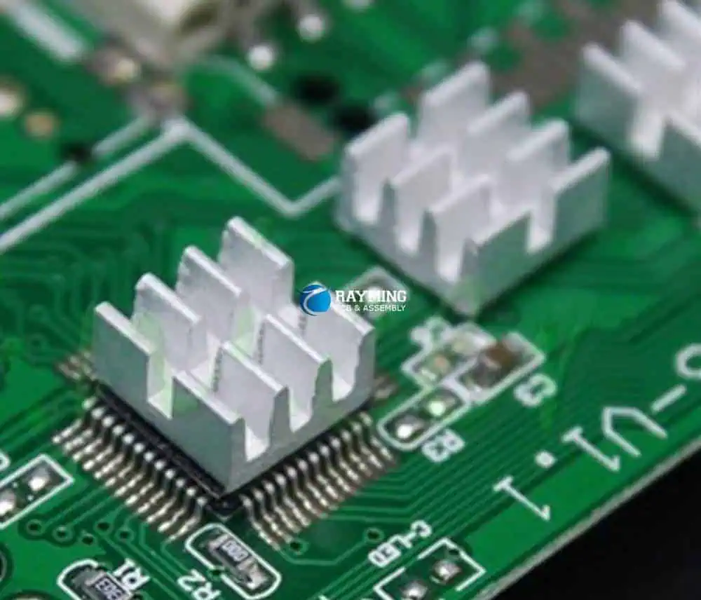
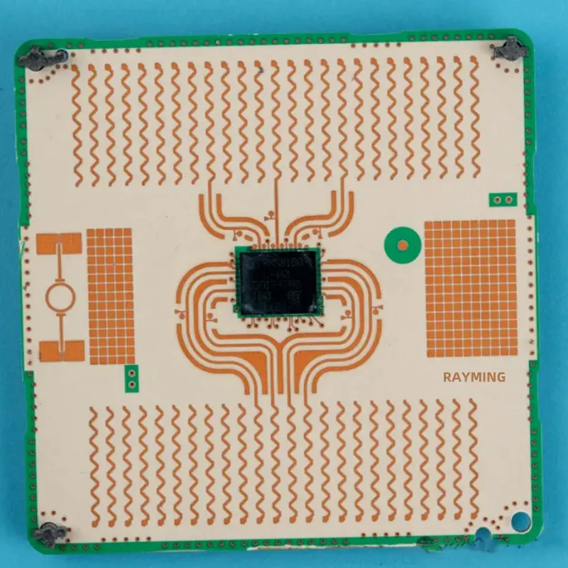
A heat sink is a passive thermal management component that absorbs and dissipates heat generated by electronic components on a printed circuit board (PCB) through thermal conduction. Heat sinks are used to cool components like power transistors, processors, power amplifiers and high-wattage LEDs that produce significant heat during operation.

Effective heat sinking is critical for maintaining device temperatures within safe operating limits and preventing damage or performance degradation. This article provides a comprehensive overview of PCB heat sink materials, design factors, attachment methods and thermal modeling considerations.

Heat Sink Basics

A heat sink comprises of a metal object, typically aluminum or copper, which is placed in contact with a heat generating component to conduct heat away and dissipate it into the ambient via fins exposed to airflow.

Key elements influencing heat sink performance include:

  • Base – Flat surface in contact with component to conduct heat from source
  • Fins – Ridges to increase surface area for more effective air convection cooling
  • Heat pipes – Closed channels containing liquid that evaporates and condenses, transmitting heat
  • Fans – Improve airflow across fins to expedite convection heat transfer
  • Thermal interface material – Grease/adhesive between sink and component to minimize thermal resistance

By efficiently sucking heat from a hot component and spreading it over a large area for air cooling, heat sinks enable reliable operation at higher powers.

Heat Sink Materials

Heat sink materials are selected for high thermal conductivity to optimize heat transfer from the heat generating component. Common materials include:

  • Aluminum – Offers excellent conductivity (200 W/mK) at low cost and weight. Most common sink material.
  • Copper – Very high conductivity (400 W/mK) but heavier and costlier than aluminum. Often used in high performance contexts.
  • Steel – Low cost but moderate conductivity (50 W/mK). Used when weight is not critical.
  • Silicon carbide – Lightweight with high conductivity (120 W/mK). Used in aerospace applications.
  • Diamond – Extremely high conductivity (2000 W/mK) but expensive. Used in specialized laser or semiconductor applications.
  • Ceramics – Insulating but can sustain high temperatures. Used as coating over metal cores.

Aluminum, copper and their alloys provide the best thermal performance for most electronics cooling applications.

Heat Sink Design Factors

Key aspects considered when designing an effective PCB heat sink include:

  • Thermal resistance – Should be low enough for required heat dissipation capacity. Depends on material and sink geometry.
  • Component power – Higher power components require greater heat flux capability.
  • Allowable temperature rise – Maximum permissible rise over ambient temperature.
  • ** Mounting method** – Conduction improved with thermal interface material and securing method.
  • Airflow – Natural or forced convection with fans impact heat transfer rate.
  • Size constraints – Physical dimensions may limit fin count and surface area.
  • Cost – Less expensive materials like aluminum often suffice for thermal needs.
  • Corrosion resistance – Sink materials should avoid corrosion over product lifetime.

Optimized heat sink design requires balancing these factors for effective thermal performance at reasonable cost.

Heat Sink Attachment Methods

Integrating heat sinks onto PCBs requires careful mounting provisions to minimize thermal resistance from component to heat sink:

Adhesives

  • Thermal adhesive physically attaches sink to component surface or package
  • Adhesive fills air gaps, improving thermal conduction
  • Silicone, epoxy or acrylic adhesive types available

Clips

  • Metal spring clips clamp sink securely onto component
  • Avoid applying excessive pressure to avoid damage
  • Clips allow sink detachment for component replacement/repair

Screws

  • Secure heat sink firmly to board or component using screws
  • Use insulation bushings/washers to prevent electrical shorts

Soldering

  • Reflowing solder paste permanently solders heat sink to lands around component
  • Provides robust thermal conduction path
  • Makes rework or repairs difficult

Adhesives, clips and screws allow some rework capability while soldering creates a permanent joint.

Thermal Interface Materials

Thermal interface materials (TIMs) are often inserted between the component and heat sink to minimize thermal resistance by filling microscopic air pockets that would otherwise hinder conduction:

  • Thermal greases – Silicone or ceramic pastes squeeze into surface irregularities. Require clamping pressure.
  • Thermal pads – Soft conductive sheets conform to surfaces. Some are dry applied, others use adhesive backings.
  • Phase change compounds – Wax-like materials melt during operation to fill gaps and voids.
  • Epoxy tapes – Adhere to surfaces and set to durable bond. Withstand scrubbing.

Applying the right amount ensures optimal conduction without air voids while avoiding excess amounts that increase resistance.

Heat Sink Fin Design

Fins provide the heat dissipating surfaces enabling convection cooling of heat sinks. Fin design parameters include:

  • Fin thickness – Thicker fins conduct heat better but add weight and material cost. Around 3mm is typical.
  • Fin height – Taller fins expose more surface area to airflow which increases heat dissipation.
  • Fin length – Longer fins increase exposed area but can be prone to bending/damage.
  • Fin density – Higher fin density boosts heat transfer but also increases air resistance. Around 5-10 fins per inch is common.
  • Fin shape – Rectangular or tapered fins affect airflow resistance and heat transfer characteristics.
  • Surface treatment – Textures, microstructures or coatings that increase surface area improve heat transfer.

Computer optimized fin shapes and patterns customized for the thermal profiles and airflow conditions enable maximum heat transfer.

Forced Convection Cooling

In forced convection, fans are mounted over heat sinks to dramatically improve airflow:

  • Axial fans – Most common. Direct air flow along length of fins.
  • Blowers – High pressure fans pushing air through dense fin arrays.
  • Centrifugal fans – Circulate air perpendicular to board expelling heat from enclosures.

Forced convection multiply heat transfer 5-10x compared to natural convection. The right fan needs to be matched to the impedance of the heat sink and airflow restrictions around board.

Heat Sink Modeling and Simulation

Heat sink designs are optimized using thermal modeling and computational fluid dynamics simulations. Important analysis parameters include:

  • Flow trajectories – Visualizes airflow patterns through heat sink for uniform distribution.
  • Pressure maps – Indicates high or low pressure zones causing flow resistance.
  • Air velocity – Quantifies airflow speed through fins ensuring sufficient ventilation.
  • Temperature mapping – Predicts localized heating across component, TIM and sink to identify hot spots.
  • Thermal gradients – Heat dissipation difference between base and fin tips should not exceed critical levels.

Such modeling ensures effective heat spreading from component to fins and no localized overheating, leading to optimal heat sink performance.

Heat Sink Applications

Heat sinks are ubiquitously used on PCB assemblies with high power dissipation components:

Power Supplies

  • Switching transistors and regulators
  • AC/DC rectifiers and converter ICs
  • Bus capacitors

Motor Drives

  • IGBTs and power MOSFETs
  • DC/AC inverters
  • Braking resistors

Servers

LEDs

  • High brightness LEDs in lighting or displays
  • LED drivers

Audio Amplifiers

  • Output transistors
  • High wattage audio ICs

Industrial

  • PLC system controllers
  • Power monitoring equipment
  • Motor servo amplifiers

Any application needing to cool components dissipating over 1-2W can benefit from appropriately designed heat sinks.

Heat Sink Design Process

A typical workflow for designing an effective PCB heat sink involves:

  1. Determine maximum component power dissipation and ambient temperature.
  2. Estimate required heat sink thermal resistance from junction to ambient.
  3. Select candidate heat sink considering tradeoffs like performance, size and costs.
  4. Model heat sink in simulation software and optimize fin parameters.
  5. Simulate thermal performance under worst-case ambient temperatures and airflows.
  6. Verify adequate margin between model results and component temperature limits.
  7. Measure thermal performance on prototypes under real-world conditions.
  8. Iterate heat sink design as needed if measured results exceed thermal limits.
  9. Qualify final design across application operating conditions to ensure reliability.

Careful thermal design upfront prevents expensive redesigns and ensures equipment lifetimes and reliability goals are achieved.

Heat Sink Design Guidelines

Here are some best practice guidelines for developing effective heat sinks on PCBs:

  • Budget adequate clearance around heat sink for unrestricted airflow.
  • Orient heat sink to align with existing or forced airflows across the board.
  • Balance thermal dissipation needs with heat sink footprint constraints.
  • For ICs, maximize sink contact surface area overlid or exposed pad area.
  • Use thermally conductive interface materials to minimize contact resistance.
  • Secure heat sink firmly onto component using screws, clamps or soldering.
  • Verify heat sink isolation from any charged components to prevent shorts.
  • Monitor temperatures during testing to validate thermal design margins.
  • Consider adding redundancy with secondary heat sinks, thermal vias and ground planes.
  • Oversize slightly to account for degradation over product lifetime.

Conclusion

Heat sinks are an essential component enabling reliable operation of electronics required to dissipate substantial amounts of power. Their ability to efficiently conduct and spread heat using metallic materials with optimized fin geometries prevents device overheating.

With continually increasing power densities in modern PCBs driven by trends like wide bandgap semiconductors, wireless charging and high-speed ICs, effective thermal management using heat sinks, active cooling and thermal-aware design practices becomes mandatory.

The electronics industry will continue relying extensively on heat sink innovations spanning materials, 3D geometries, adaptive algorithms and computer simulations to sustain the relentless pace of advancement in energy efficient, high-performance electronic systems.

Frequently Asked Questions

Q: What is a heat sink in PCBs?

A: A heat sink is a metallic thermal management component like an aluminum plate that absorbs and dissipates heat from hot electronic components on a PCB through conduction and air convection.

Q: Why are heat sinks needed on PCBs?

A: Heat sinks prevent electronic components from overheating by efficiently conducting heat away and spreading it over fins exposed to airflow. This maintains safe device temperatures.

Q: What materials are used to make PCB heat sinks?

A: Aluminum and copper are most common due to high thermal conductivity. Other materials include steel, silicon carbide, diamond and ceramics.

Q: How are heat sinks attached to PCBs?

A: Common attachment methods include thermal adhesive, spring clips, screws and soldering. Thermal interface materials minimize contact resistance.

Q: How are heat sinks designed and simulated?

A: Important factors like airflows, fin parameters and thermal gradients are modeled using CAD and computational fluid dynamics simulation to optimize heat transfer.

Why Heat Sink PCBs are Important in Electronic Circuits

All electrical components in a circuit produce heat while the circuit is functioning. High-power devices such as power transistors, LEDs, and lasers produce heat. Some of these components can’t dissipate heat since they have a low dissipation capability.

Heat build-up in the component can result in total failure or premature failure in the device. Therefore, heat sink boards are a perfect way to conquer these problems. These circuit boards are used in most applications because of their cooling functions. PCB manufacturers include a heat sink in PCB due to the numerous benefits it offers.

Passive Heat Exchange

Heat sink PCBs feature a large surface area that cools off. These boards act as passive heat exchangers. The component of a device that can’t control its temperature needs heat sink PCBs. To improve performance, every heat in a component of an electronic circuit must be dissipated. This will help to prevent the component from experiencing any failure.

Maintains Thermal Stability

Heat sinks in PCB help to maintain thermal stability in any electronic device. Thermal stability is very important for electronic components of any circuit. Heat sink PCBs can survive in any temperature because of their cooling ability. This is a major reason these PCBs are employed in high-performance applications.

Heat sinks don’t only dissipate heat; they also provide heat during low temperatures. They do this by generating thermal energy for the smooth functioning of the circuit.

Spreads heat

Heat sinks serve as heat spreaders in some applications. For instance, a heat sink PCB functions as covers on the memory of a computer. Heat sinks also help to cool off the graphic processors and CPU of computers.

Prevents system failure

Heat sinks prevent system failure in a circuit. The absence of a heat sink can cause the failure of components. It is advisable to implement a heat sink in a PCB to prevent overheating. Component failure is one of the common problems of electronics or electrical devices.

Different types of mechanical and electronic devices generate heat which heat sinks absorb. Heat sink PCBs play significant roles in mechanical, electronic, nuclear, and solar processes.

Types of Heat Sink

Heat sinks are available in various types. Each of these types has its function. However, they share some common characteristics or features. Heat sinks are mostly made from metal like aluminum or copper. The commonest designs for a heat sink are the fin layout. Some versions utilize stamping and pins to increase the surface area and heat transfer rate.

Passive heat sink

A passive heat sink doesn’t feature additional products while cooling a component. It isn’t assisted by additional processes. These heat sinks don’t have any mechanical components. They dissipate heat through the convection process. When you use this heat sink on PCB, it gives reliable results.  Experts recommend that engineers should maintain the flow of air across the fins of this heat sink.

Passive heat sinks serve as a standalone solution since they don’t use other cooling methods. These heat sinks are bigger than active heat sinks. Passive heat sinks disperse absorbed heat via the direct contact between them.

Active heat sink

This type of heat sink uses additional products to enhance its cooling capacity. Active heat sinks use powered processes like water pumps and fans. These processes or products help to increase the heat transfer rate. In some electronic systems, these coolers run off the internal power supply. This type of heat sink isn’t ideal for long-term applications. This is because it has moving parts.

Active heat sinks make use of one or more fans. These fans are either above or on the side of the fin stack. Some advanced active heat sinks use water to transfer heat from a source.

Types of Heat Sink Based on Material

Aluminum heat sink

An aluminum heat sink is a less expensive choice for heat sinks. This type of heat sink is designed in a way that the generated heat escapes via some thin metal fins. Aluminum is the commonest material used in heat sinks. The thermal conductivity of aluminum is different from copper. The thermal conductivity of the metal affects the heat sink’s heat transferring capacity.

Copper heat sink

Most heat sinks are made of copper. Copper is a good thermal conductor and has got great heat transfer capabilities. This type of heat sink draws away heat from the device you want to cool. Heat sink PCB made of copper is more expensive.  Most PCB heatsink designs use copper.

Pinned heat sink

A pinned heat sink is an alternative design fin heat sink. The core block of the pinned heat sinks features a cluster of rods or pins that extends outward or upward. This type of heat sink has a better overall surface. But, they don’t offer good performance improvement in most applications.

Finned heat sink

This type of heat sink is designed from a block of metal. This metal is available in a large number of thin plates that extend away from the central block. Finned heat sink features a better surface area. This makes it more effective in transferring heat away from the component. The manufacturing and designing of this heat sink involve either die-cast or forged models.

Heat Sink Types Based on Manufacturing Techniques

Circuit board heat sink

Various manufacturing methods are used in manufacturing heat sinks.

Stamped heat sink

This type of heat sink features stamped metals. These metals can form a certain shape. The stamp designs the heat sinks anytime metal moves via the stamping machine. Stamped heat sinks are ideal for low-power applications.

Bonded heat sink

This type of heat sink is ideal for large applications that demand sensible performance. Bonded heat sinks are designed by combining separate fins of metal to the heat sink’s base. There are two different methods for doing this. They are the brazing and the thermal epoxy methods.

Skived heat sink

Skived heat sinks employ skiving for their manufacturing. Skiving is the use of fine blocks of metals for manufacturing heat sinks. Skived heat sinks can be high or medium-performing heat sinks.

Swaged heat sink

Swaged heat sinks are medium-performing heat sinks. Swaging is a manufacturing technique that involves a cold working forging process. However, it can undergo a hot working process.

Forged heat sink

Forging involves utilizing compressive forces. This technique is used for manufacturing aluminum and copper heat sinks.

Machining heat sink

This type of heat sink uses a machining process for its manufacturing. Gangsaw helps to eliminate a block of material. This type of manufacturing process is expensive since a lot of metal may waste.

Applications of Heat Sink PCB

Heat sink PCBs are used in several applications due to the functions they perform. These circuit boards are ideal for high-performance applications. They are also suitable for use in devices that produce a high amount of heat.

LEDs

Heat sink PCBs are commonly used in Light-emitting diodes (LED). These PCBs provide effective cooling for LED pcb. Heat sink circuit boards prevent excess heat from damaging LEDs. Most high-power LEDs feature heat sink PCBs.

Computers

Heat sink PCBs are a common component of computers. The CPU of computers needs a heat sink. Electrical activity in the CPU produces a good amount of heat. This may cause damage to the chipset. A heat sink helps to offer a good path for heat to pass through. The CPU comes with a heat sink. Some manufacturers use a particular type of heat sink for their CPUs.

Industrial facilities

Most industrial devices generate heat while in use. Therefore, a heat sink PCB is ideal for use in industrial equipment. Heat sinks are connected on a circuit board because of their cooling properties. They reduce the amount of absorbed heat in a mechanical device while running.

Soldering

During the soldering process, heat sinks help to protect electronic components. Some components need the protection of a heat sink during soldering.

Consumer products

Heat sink PCBs are used in most consumer products. Some electronic devices in the home come with heat sinks. This is because some components of these devices generate a lot of heat. Therefore, heat sink PCBs help to dissipate heat in these devices.

The Limitations of Heat Sink PCB

FULL PCB MANUFACTURING Quote

The cooling of electronic devices is important for their long-lasting function. The need for circuit bard cooling has continued to increase. Heat Sink PCBs help to dissipate heat in electronic devices. The importance of the use of heat sinks in PCBs can’t be overemphasized.

There are different types of heat sink PCB with different thermal resistance values. These PCBs ensure cooling.  Heat sink PCBs have their challenges. One of the major challenges is the joining of the circuit board with the heat sink.

Another challenge is the aerial use of thermal adhesive without air pockets between the components.  The properties of the thermal adhesive caused this problem. However, thermal engineers achieved good distribution by using pressure pins. The vacuum joining process presents a reliable result.

The dissipation of heat loss from chips is a major issue for developers. There are several ways to link a heat sink to the source of the heat. The fabrication of a heat sink PCB involves creating a separate metal heat sink. Then, manufacturers use liquid adhesive to attach this heat sink to a finished board.

Heat Sink Dissipation Method

Heat sink PCBs use some methods to dissipate heat which are:

  • Heat transfer compounds
  • Metal heat-conducting plate
  • Higher copper thickness
  • Metal core

Heat transfer compounds

For heat sink PCBs, fabricators use a screen-printing procedure to apply the heat transfer compound to the silkscreen. The layer’s thickness ranges between 100 – 150 μm.

Metal core

Rather than using the standard base material, a copper or aluminum sheet is used here.  A prepreg is used to laminate a copper foil onto a metal core.

Higher copper thicknesses

When it comes to thick-copper boards, the copper absorbs the heat and directly dissipates it. The copper thicknesses are 400 μm, 210 μm, and 105 μm. This method involves high-cost production since the conductor structure requires much effort.

Metal heat-conducting plate

In this method, a heat sink PCB goes through the standard production process. Manufacturers use a prepreg to press mold the PCB to the metal heat-conducting plate.

Factors to Consider in Heat Sink Design

The design of a PCB is a very complex process. The importance of heat sinks in PCB can’t be overstressed. Engineers need to consider some factors when implementing a heat sink on PCB. Heat sinks transmit thermal energy from electronic components into a cooling medium.

Several factors determine the performance of heat sinks. The material’s thermal conductivity and attachment method are some of these factors. Engineers can determine the parameters of a heat sink via analysis and modeling.

Heat sink materials

Alloys, aluminum, and copper are materials used for designing heat sinks. Copper is a good thermal conductor that resists corrosion and absorbs heat. This material is ideal for heat sinks due to its properties. However, it is a more expensive option.

Diamond is another ideal material for thermal applications. This is because it features lattice vibrations. Another alternative is the bonding of aluminum and copper. In this case, aluminum is the dominant material due to its lightweight. This is a perfect combination for heat sinks in computers.

Heat sink fins

Heat sinks feature fins in their design. These fins offer the necessary surface area for heat dissipation. They cool the heat source. The fin’s efficiency determines the performance of the heat sink. Once there is a flow of heat through the fin the temperature reduces from the base.

The arrangement and location of the fins also affect the performance of the heat sink. The design and shape of the fins will greatly determine the heat sink’s performance.

Thermal resistance

Thermal resistance determines how heat sinks perform. This factor determines heat flow. In order to achieve an efficient heat sink, the thermal management system needs to be combined with a cost-effective design.

Attachment methods

There are different methods of attaching heat sinks to the component of a device. Using the appropriate method helps to enhance the heat sink’s thermal performance. Thermal tape, standoff spacers, epoxy, and flat spring clips are examples of attachment methods.

Characteristics of a Good Heat Sink

A good heat sink features some characteristics that make them ideal in most applications. The characteristics of this heat sink are;

  • Heat dissipation correlates with the temperature difference between the ambient temperature and the device.
  • The mounting method is very critical. It uses screws rather than utilizing glue, clips, or sticky tape.
  • Heat dissipation correlates with the fins’ surface area. Therefore, it should have a very large surface.
  • Flat surface must have contact with the source of heat. This is very important as it allows a layer of thermal compound to minimize thermal resistance between the devices.
  • Heat sink design must enable free flow of air through the fins.

PCB Heat Dissipation Techniques

As PCBs are a core aspect of electronic devices, heat dissipation techniques are very important. Most electronic devices produce heat while they are running. Heat sink PCB helps to spread heat across components in a circuit. Below are some heat dissipation techniques;

Use cooling fans and heat sinks

If a printed circuit board generates a high amount of heat. You will have to incorporate fans and heat sinks in the design. Manufacturers attach heat sinks to components that produce the most heat. Power transistors, CPUs, and voltage regulators are such components. Here, the heat sinks are on the PCB. You can also install a cooling fan to help discharge the hot air in the environment.

Thermal via arrays

You can make use of thermal via arrays to transform a PCB into an onboard heat sink. The idea behind this is for flow of heat from the components to the copper area. Then the heat dissipates via the air from the vias.

Thermal via array must feature a large diameter to allow effective dissipation of heat. The vias must feature padded holes that connect to the copper area. More thermal vias also help dissipation of heat.

Use wider traces

Ensure you increase the trace’s width to improve heat dissipation to the air. This will help to reduce the trace’s thermal resistance and also minimize heat spots. Good copper trace thickness can offer a low impedance path.

These heat dissipation techniques are very important in electronics. Heat sinks play a significant role in the dissipation of heat in electronic devices. Components like power transistors and microcontrollers often generate heat. This happens especially when the load current rises.

Frequently Asked Questions

How do you calculate heat sink performance?

The performance of heat sinks is also known as thermal resistance. It is measured in °C/W. If a heat sink has a thermal load of 50W and the heat source rises by 20 °C. One can say the heat sink rating is 20/50 °C/W. This is equal to 0.40 °C/W.

How can the impact of heat on PCBs be minimized?

To do this, separate heat-sensitive components and heat-generating ones on the PCB. This can help you concentrate heat dissipation to a certain area. Doing this will also prevent the heat from going towards the heat-sensitive components. Place heat-producing components on the top when mounting the PCB vertically. You can reduce the heat dissipation path by placing the components towards the PCB’s edge.

What is a thermal simulation in PCB?

Thermal simulation locates the temperature of a thermal hotspot in a printed circuit board. Locating the thermal hotspots help to prevent the risk of failure in devices.

Conclusion

Electronic components can operate within a definite temperature range. When the temperature around these components rises beyond the upper limit, there can be a breakdown. Excessive heat can have a negative effect on the performance of the component.

For instance, MCU uses more energy at high temperatures. The lifespan of an electronic device will reduce if it is exposed to too much heat.  Too much heat can lead to premature failure of components. Therefore a heat sink PCB is an ideal choice for most electronics.

What Is Xilinx XC7A35T-2FGG484i?

Xilinx XC7A35T-2FGG484i

The Xilinx XC7A35T-2FGG484i device belongs to the low-cost, low-power Artix-7 family of FPGAs built on 28nm high-performance, low-power (HPL) process technology. With 33K logic cells, 125MHz DSP slices and 12.5Gbps transceivers, the XC7A35T provides an optimized blend of programmable logic, real-time processing, high-speed I/O and power efficiency ideal for applications including motor control, functional safety, video bridging, software defined radio, broadcast camera links and ultrasound equipment.

This article provides a technical overview of the XC7A35T architecture, available resources, target applications, design flow and benefits for system designers.

XC7A35T-2FGG484i Overview

The Xilinx XC7A35T belongs to the Artix-7 family which spans small to large capacity FPGAs and SoCs supporting space constrained embedded applications. Key attributes include:

  • 33K logic cells based on look-up tables (LUTs) as the basic logic building block
  • 125MHz DSP slices with 25 x 18 multipliers
  • 12 dual-channel gigabit transceivers operating up to 12.5Gbps
  • 258 maximum user I/Os
  • High speed memory interface supporting DDR3 at up to 1600Mbps
  • Configurable mixed-voltage I/O banks
  • High performance, low power 28HPL process

The 2FGG484 package designates a compact 17×17 mm 484-ball flip-chip grid array with 1.0mm ball pitch. It provides ample connectivity for embedding the Artix-7 in space constrained embedded systems.

XC7A35T Internal Architecture

The Artix-7 family architecture balances high density programmable logic fabric along with frequently needed hardened blocks for embedded systems.

Programmable Logic Fabric

The core programmable logic is built from slices containing LUTs, flip-flops, multiplexers, arithmetic and wide function generators. Key attributes:

  • 6-input LUTs efficiently implement logic functions using only a single LUT per slice
  • Flip-flops for sequential logic – register, shift register or latch operation
  • Carry logic for arithmetic functions
  • Block RAM for distributed memory storage

DSP Slices

The 125 embedded 18×25 multipliers and 48-bit accumulators enable high-performance arithmetic processing.

Block RAM

1.9Mb of distributed 36Kb block RAM provides on-chip data storage with built-in FIFO support.

Transceivers

Up to 12 multirate transceivers operating at up to 12.5Gbps support high-speed serial I/O connectivity.

PCI Express

Two integrated Gen2 PCIe blocks enable direct chip-to-chip communication.

Multi-Standard I/Os

The configurable I/O blocks allow matching electrical interfaces to a wide range of standards including LVDS, HSTL and SSTL.

XC7A35T Target Applications

The XC7A35T is designed to meet the needs of compute-intensive, connectivity-centric embedded systems across industrial, automotive, communications, aerospace/defense and functional safety applications:

Industrial Automation

  • Motor drives
  • Inverters
  • PLC systems
  • Process control
  • Machine vision

Automotive

  • Camera links
  • RADAR/LiDAR processing
  • Driver assistance systems
  • Functional safety

Wireless Infrastructure

  • FMCW radar modems
  • Microwave radio links
  • Small cell baseband processing
  • Optical network cards

Aerospace and Defense

  • RADAR and sonar processing
  • Communications monitoring
  • Video tracking systems
  • Encryption/decryption

Test and Measurement

  • Protocol analyzers
  • Video test signal generators
  • High-precision metrology

The cost-optimized programmable logic balanced with integrated processing enables these demanding applications.

XC7A35T-2FGG484i Benefits for Designers

The XC7A35T architecture and capabilities provide hardware engineers with several advantages:

High Performance

  • 33K logic cells enables implementation of complex digital logic
  • 125MHz DSP slices accelerate math-intensive algorithms
  • 12.5Gbps serial connectivity to transfer high-speed data

Power Efficiency

  • 28nm process enables low static and dynamic power consumption
  • Integrated blocks reduce external components lowering overall system power

Functional Safety

  • Configuration CRCs and error detection circuitry improve reliability

Scalability

  • Multiple density, I/O and transceiver options within Artix-7 family

Cost

  • Mature 28nm process combined with optimized architecture provides low cost

For demanding connectivity-centric embedded systems, the XC7A35T delivers high throughput signal processing coupled with flexible programmable logic at very compelling price points.

XC7A35T Design Flow

Xilinx provides powerful design tools for programming the XC7A35T FPGA:

  • Vivado Design Suite – Enables system design, logic synthesis, placement and routing
  • Vivado IP Integrator – Connects intellectual property blocks into integrated designs
  • SDSoC Development Environment – Supports C/C++ embedded software design
  • Vivado HLS – Converts C/C++ code into tuned logic implementations
  • System Generator – Implements high-performance DSP designs
  • ChipScope Pro – Provides low-level debug capability

The typical design flow involves:

  1. Create register transfer level (RTL) code defining desired functionality
  2. Run RTL simulations to verify correct behavior
  3. Synthesize RTL into Xilinx primitives using Vivado synthesis
  4. Place and route design to map into XC7A35T physical resources
  5. Generate bitstream representing complete FPGA configuration
  6. Program finished bitstream into XC7A35T device
  7. Validate operation and timing in real system

XC7A35T vs. Larger FPGAs

Xilinx Chips
Xilinx Chips

It is useful to contrast the XC7A35T against higher density FPGAs like the Kintex-7:

Programmable Logic

  • XC7A35T offers 33K logic cells using 6-input LUTs
  • Kintex-7 provides up to 474K logic cells using 6-input LUTs

Transceivers

  • Both support up to 16 transceivers operating at 12.5Gbps

Memory Interfaces

  • Both support external DDR3 memory interfaces up to 1600Mbps

DSP Slices

  • XC7A35T – 220 DSP slices operating at 125MHz
  • Kintex-7 – Up to 3600 DSP slices at 500MHz+

Cost

  • XC7A35T optimized for low cost high volume applications
  • Kintex-7 costs approximately 40% higher

For applications where power efficiency and unit costs are critical, the XC7A35T offers the ideal programmable logic solution. When maximum performance is mandatory, Kintex-7 provides superior DSP and memory interfacing capabilities.

Conclusion

By integrating abundant I/Os, DSP slices, serial transceivers, block RAM, and PCIe blocks together with cost-optimized programmable logic fabric, the Xilinx XC7A35T-2FGG484i provides an extremely capable chip foundation for next-generation industrial controls, motor drives, functional safety systems, communications infrastructure, test instrumentation and aerospace/defense electronics.

For embedded systems engineers challenged with staying competitive on performance, capabilities, power efficiency and unit costs, the Artix-7 family offers an invaluable platform for accelerating innovation and progress from concept to deployed solution.

Frequently Asked Questions

Q: What is the Xilinx XC7A35T FPGA?

A: It is a low-cost, low-power Artix-7 series FPGA with 33K logic cells, 125MHz DSP blocks and 12.5Gbps transceivers built on a 28nm fabrication process.

Q: What are some key components of the XC7A35T architecture?

A: This includes programmable logic fabric using 6-input LUTs, 220 DSP slices, 1.9Mb of block RAM, up to 16 transceivers, PCIe blocks, and configurable mixed-voltage I/O.

Q: What kinds of applications can the XC7A35T FPGA address?

A: Target applications span industrial automation, motor drives, functional safety systems, wireless infrastructure, broadcast video, test instrumentation.

Q: How does the XC7A35T compare against larger FPGAs like Kintex-7?

A: Kintex-7 offers approximately 40% higher logic capacity and performance but at a greater cost. XC7A35T optimizes cost and power efficiency.

Q: What design tools support programming XC7A35T FPGAs?

A: Xilinx’s Vivado Design Suite supports the end-to-end flow from RTL design entry to layout and implementation culminating in bitstream generation.

What Is Xilinx XC6SLX45T-2FGG484i ?

Xilinx XC6SLX45T-2FGG484i

The Xilinx XC6SLX45T-2FGG484i is a mid-range capacity Spartan-6 series field programmable gate array (FPGA) fabricated using a low-power 45nm process. This particular device provides a balance of programmable logic resources, abundant I/Os and hardened functional blocks ideal for applications including industrial networking, motor control, video processing, software defined radio and functional safety systems.

This article covers the XC6SLX45T architecture, available resources, target applications, design considerations and benefits for electronics engineers.

XC6SLX45T-2FGG484i Overview

The Xilinx XC6SLX45T belongs to the Spartan-6 FPGA family built on a 45nm node manufacturing process. Key attributes include:

  • 45K logic cells featuring 6-input LUTs as the basic logic building block
  • 216 DSP slices optimized for arithmetic and signal processing tasks
  • 12.2Mb of distributed block RAM for on-chip data storage
  • 6.6Gbps serial transceivers for high-speed chip-to-chip communication
  • 500+ user I/Os supporting dozens of electrical interfaces
  • Advanced power management techniques for low static and dynamic power
  • Industrial temperature rating of -40°C to +100°C

This combination of programmable logic, hardened blocks and I/O enables implementation of complex digital systems with high throughput capabilities.

The 2FGG484 package designates a 23x23mm 1.0mm pitch 484-ball fine-pitch BGA with 7.5mm ball height. This compact form factor provides adequate I/Os for most applications in a small surface mount package.

XC6SLX45T FPGA Internal Architecture

The Spartan-6 architecture is optimized to deliver balanced programmable logic capabilities together with essential integrated peripherals useful across many applications.

Configurable Logic Blocks

The core programmable logic fabric is built from Configurable Logic Blocks (CLBs). Each CLB includes:

  • 2 Slices, each with 4 6-input LUTs and 8 flip-flops
  • Arithmetic carry logic
  • Distributed RAM for local storage

CLBs are interconnected by a flexible routing fabric enabling complex digital logic implementation.

DSP Slices

216 dedicated 18×18 multipliers and 48-bit accumulators accelerate math-intensive functions like filters, FFTs and video processing.

Block RAM

12.2Mb of distributed 36Kb block RAM provides on-chip data storage. Built-in FIFO support, byte write enable and ECC mode simplifies memory management.

Clock Management

Digital Clock Managers (DCMs) and Mixed Mode Clock Managers (MMCMs) provide self-calibrating, fully digital solutions for distributing and manipulating clocks across the device.

I/O Blocks

Configurable I/O blocks around the periphery of the FPGA enable interfacing to a wide range of electrical standards including LVTTL, LVCMOS, LVDS and SSTL. Maximum I/O speed reaches 1.6Gbps.

Transceivers

Integrated serial transceivers operate at up to 6.6Gbps supporting protocols like PCIe, Gigabit Ethernet, CPRI and Serial RapidIO.

XC6SLX45T Target Applications

The XC6SLX45T provides an ideal blend of capabilities for connectivity-oriented embedded applications including:

Industrial Networking and Motor Control

  • EtherCAT slaves
  • Functional safety systems
  • Servo motor control
  • Human machine interface (HMI)
  • SCADA systems

Wireless Communications

  • 4G LTE radio control
  • Small cell baseband processing
  • Software defined radio
  • Microwave radio links

Broadcast Video

  • Video overlays
  • Format conversion
  • Frame synchronization
  • Distribution amplifiers

Medical and Scientific

  • DNA sequencing
  • Particle detection
  • Weather monitoring
  • Ultrasound and MRI processing

Aerospace and Defense

  • RADAR signal processing
  • Mission control
  • Navigation algorithms
  • Encryption/decryption

The XC6SLX45T balances performance, power and costs for connectivity-centric applications requiring reasonable logic capacity.

XC6SLX45T-2FGG484i Benefits for Designers

Xilinx FPGA distributor

For hardware engineers, the XC6SLX45T-2FGG484i provides several compelling advantages:

Performance

  • 45K logic cells enables complex digital system implementation
  • DSP slices accelerate math-intensive algorithms
  • 6.6Gbps transceivers allow high-throughput serial I/O

Low Power

  • 45nm fabrication optimized for low static and dynamic power
  • Suspend mode reduces power consumption to just 11mW

Reduced BOM

  • 12Mb RAM and DSP blocks minimize external memories and processors
  • Transceivers eliminate external SERDES ICs

Design Security

  • Bitstream encryption secures compiled designs from copying

Reliability

  • Industrial -40°C to +100°C temperature rating

While balancing cost, the XC6SLX45T provides ample functionality for applications at the intersection of programmable logic, real-time processing and high-speed interfacing.

Design Tools and Methodology

Xilinx offers a mature tool flow for programming the XC6SLX45T FPGA:

  • ISE Design Suite – enables design at register-transfer level (RTL) using Verilog or VHDL
  • Embedded Development Kit (EDK) – creates hardware/software systems using the Microblaze soft core CPU
  • ChipScope Pro – provides debug capability with real-time signal visualization
  • iMPACT – programs bitstream files into the FPGA through common interfaces

Typical design steps include:

  1. Create register-transfer level (RTL) code to define desired functionality
  2. Run RTL simulations to verify correct behavior
  3. Synthesize RTL into Xilinx primitives using ISE tools
  4. Verify timing, power and utilization meet requirements
  5. Generate bitstream file representing complete FPGA configuration
  6. Program finished bitstream into the XC6SLX45T-2FGG484i FPGA

XC6SLX45T vs. Larger FPGAs

It is useful to contrast the XC6SLX45T against larger capacity FPGAs like Xilinx’s Virtex-6:

Programmable Logic

  • XC6SLX45T provides 45K logic cells using 6-input LUTs
  • Virtex-6 offers up to 360K logic cells using 6-input LUTs

Transceivers

  • XC6SLX45T – 6.6Gbps data rate, up to 16 channels
  • Virtex-6 – Up to 11.2Gbps, 96 channels

Memory

  • Both support similar 36Kb block RAM capacities
  • Virtex-6 adds 512Mb – 1Gb dedicated DDR3 memory interfacing

DSP Slices

  • XC6SLX45T – 216 slices @ 25 x 18 multipliers
  • Virtex-6 – Up to 2016 slices @ 25 x 18 multipliers

Cost

  • XC6SLX45T optimized for low cost by removing top-tier features
  • Virtex-6 costs approximately 4-5X higher

For applications with intelligence distributed across multiple nodes, XC6SLX45T provides the optimal blend of capability and affordability.

Conclusion

The Xilinx XC6SLX45T-2FGG484i hits the sweet spot between programmable logic density, real-time processing capability and high-speed interfacing required in industrial controls, motor drives, communications infrastructure and functional safety systems.

Built on a low-power 45nm process, the XC6SLX45T balances logic capacity, abundant I/Os, DSP blocks and serial transceivers in a compact surface mount package – making it an extremely versatile chip for connectivity-centric applications demanding reasonable performance.

Frequently Asked Questions

Q: What is the Xilinx XC6SLX45T FPGA?

A: It is a low-cost Spartan-6 series FPGA with 45K logic cells, DSP slices and 6.6Gbps transceivers, built on a 45nm fabrication process.

Q: What are the key elements in XC6SLX45T architecture?

A: This includes 45K logic cells using 6-input LUTs, 216 DSP slices, 12Mb of block RAM, MMCM clock management, and up to 16 serial transceivers.

Q: What design tools can be used for programming XC6SLX45T FPGAs?

A: Xilinx offers the ISE Design Suite for RTL design entry, ChipScope Pro for debug, and iMPACT for final bitstream programming.

Q: What are some common applications for the XC6SLX45T FPGA?

A: Target applications include industrial motor control, functional safety systems, wireless infrastructure, broadcast video, aerospace electronics.

Q: How does XC6SLX45T compare to larger FPGAs like Virtex-6?

A: Virtex-6 offers 4-5X higher logic capacity and transceiver count but costs substantially more. XC6SLX45T provides an optimized cost/capability blend.

What is a Printed Circuit Board ( PCB )?

military rogers pcb board

What is a Printed Circuit Board?

A Printed Circuit Board (PCB) is the foundation of modern electronics, serving as both an electrical connector and a mechanical support for electronic components. Here’s what you need to know:

  1. Structure:
    • PCBs consist of alternating layers of conductive copper and insulating material.
    • Conductive features include copper traces, pads, and planes.
    • Insulating layers provide mechanical structure and electrical isolation.
  2. Surface Finish:
    • A non-conductive solder mask covers the board for protection.
    • Silk-screened legends guide component placement.
  3. Manufacturing Process:
    • Inner copper layers are etched to form circuit patterns.
    • Multiple layers are laminated together to create the full stack-up.
    • The bare board is then ready for component assembly.
  4. Assembly:
    • Electronic components are soldered onto the board.
    • The completed assembly is called a PCBA (Printed Circuit Board Assembly).
  5. Purpose:
    • Creates electrical connections between components.
    • Provides mechanical support for components within a device.

PCBs are essential in creating compact, reliable electronic devices across various industries, from consumer electronics to aerospace technology.

Read more about PCB technical:

6 Layer ENIG PCB
Flex PCB
Rigid Flex PCB
Rogers PCB
Antenna PCB
HDI PCB

Types of PCBs

While rigid PCBs are the most common, there are various types of circuit boards constructed on different materials. Here’s an overview of the main PCB types:

  1. Single-sided: Components on one surface, typically with a copper ground plane on the back.
  2. Double-sided: Components on both surfaces, with each surface acting as a signal layer.
  3. Multi-layer: Internal conductive layers for signals or planes. Can be single or double-sided.
  4. Rigid-flex: Combines rigid sections with flexible polyimide ribbons, allowing for movable elements.
  5. Flex PCBs: Entirely flexible, made of polyimide ribbons. Can have mounted components like rigid PCBs.
  6. Printed flex PCBs: Flexible base with printed copper conductors, similar to flex PCBs.
  7. Metal-core PCBs: Use a metal core (usually aluminum) for improved rigidity and heat dissipation.
  8. Ceramic PCBs: Used in applications requiring high thermal conductivity.
  9. HDI PCBs: High-density interconnect boards for very high pin count components.
  10. UHDI and Substrate-like PCBs: Extremely small and dense, requiring specialized additive manufacturing processes.

Each type has unique fabrication and assembly processes. Modern ECAD software can assist in designing any of these PCB types, provided the correct design rules are applied.

PCB Manufacturing Process Overview

Strip film etching line

PCBs are fabricated using sophisticated processes optimized for high yield and reliability across large panel sizes containing multiple boards:

  • 1. Design – The PCB layout is designed in CAD software based on circuit requirements and component footprints.
  • 2. Fabrication – Blank copper-clad laminate sheets are drilled, plated and coated with photoresist. An imaging process transfers the PCB layout onto the panel.
  • 3. Etching – Exposed copper is etched away chemically, leaving only the protected circuit traces/pads. Photoresist is then stripped.
  • 4. Plating – Conductive barrel walls are plated in drilled holes to create plated through hole (PTH) interconnections.
  • 5. Solder mask – Epoxy layers are applied for insulating exposed copper traces from solder and environmental corrosion.
  • 6. Silkscreen – Paint masks are used to apply component identifiers and outlines for assembly.
  • 7. Testing – Manufacturing defects are detected using electrical test and imaging processes.
  • 8. Panelization – Individual PCBs are depanelized from the larger sheets into stand-alone boards.
  • 9. Population – Electronic components are soldered onto the boards using surface mount (SMT) and/or through-hole technologies.

These steps produce finished printed circuit boards ready for integration into electronic products and systems.

PCB Substrate Materials

The PCB substrate, also referred to as laminate, forms the base layer upon which the copper traces are fabricated. Key laminate requirements include:

  • Electrical insulation to prevent shorting between traces
  • Thermal conductivity to dissipate heat from components
  • Structural rigidity for mechanical support
  • Dimensional stability across temperature and humidity
  • Process compatibility for fabrication and assembly

Popular PCB substrate materials include:

  • FR-4 – Woven fiberglass cloth in an epoxy resin binder. Low cost, globally available.
  • CEM-1/3 – Cotton paper base material. Cost effective, suitable for low frequencies.
  • PTFE – Synthetic fluoropolymer offering highest performance but costly.
  • Polyimide – Withstands very high temperatures. Used in flex circuits.
  • Alumina – Ceramic-based; very rigid and thermally conductive for high power PCBs.
  • Metal core – Base metal layer for max heat dissipation.

The substrate choice affects PCB performance parameters, fabrication methods and ultimate application suitability.

Conductive Layers

The conducting layers provide the electrical connectivity in a PCB by etching the laminated copper foils into desired circuit patterns. Key considerations include:

  • Copper thickness – Varies from 0.5 oz (0.0007 inches) to 6 oz (0.0042 inches) or more based on current needs.
  • Foil type – Rolled copper has better flexibility but lower current capacity than electrodeposited copper.
  • Layer count – Number of conductive layers laminated determines circuit complexity. Modern PCBs can have over 30 conductive layers.
  • Layer stackup – Stacking order of power, ground and signal layers optimized for electrical performance.
  • Trace dimensions – Conductor width, spacing and thickness dictated by current, voltages and insulation needs.
  • Trace profile – Rectangular or trapezoidal cross-section optimized for production yields.

Proper layer stackup design and copper weight/density minimizes noise coupling and enables routing high speed signals across the PCB.

Plated Through Holes

PCB pattern plating line

Plated through holes (PTHs) are conductive barrels fabricated by drilling holes through the PCB layers and plating the internal walls to form electrical connections between layers. Benefits include:

  • Provides vertical interconnects through entire PCB thickness
  • Connects traces on different layers for routing signals
  • Connects internal power/ground planes for power distribution
  • Enables component leads to pass through board and solder on opposite side
  • Higher reliability and current capacity than vias

PTHs are essential for multilayer PCB construction, power delivery, attaching connectors and through-hole component soldering.

PCB Design and Layout

PCB layout involves arranging interconnects between electronic components in a physical manner that optimizes electrical performance, manufacturability, costs, reliability and other factors.

Key aspects of PCB layout include:

  • Component footprints – Land/pad geometries matching component lead configurations
  • Net routing – Interconnects between component pins implemented as traces on layers
  • Thermal management – Strategic placement and copper fills to dissipate heat
  • EMI/EMC controls – Minimizing interference and susceptibility
  • Signal integrity – Tuned trace impedance, spacing, rise times for quality signal propagation
  • Manufacturing rules – Accommodating tolerances, annular rings, fabrication constraints
  • Test points – Providing access points for validation and troubleshooting
  • Assembly considerations – Ease of component placement, orientation and soldering

Following sound PCB design practices ensures the layout can be accurately produced within budget.

PCB Assembly and Soldering

Once fabricated, a bare PCB is populated with electronic components to form a functional printed circuit assembly (PCA). The two main methods are:

Through-Hole Assembly

  • Component leads are inserted through holes in PCB body
  • Leads soldered to barrel walls of plated through holes
  • Provides strong mechanical connection

Surface Mount Assembly

  • Components directly soldered to pads on PCB surface
  • Enables miniaturization and higher density
  • Reflow soldering heats entire board for mass solder joint formation
  • Mixed SMT and through-hole assembly also widely used

For high volume production, SMT lines utilize pick-and-place machines and conveyorized reflow. Rework stations allow modifying soldered assemblies.

Key PCB Characteristics

Rogers TC350 PCB

Essential characteristics defining a PCB’s capabilities:

  • Number of conductive layers – Represents PCB complexity; more layers provide higher component density
  • Laminate material – Determines electrical, thermal, mechanical characteristics
  • Trace/space – Narrowest conductor width and gap; 5 mil line/space common in commercial PCBs
  • Finished copper thickness – After plating; affects current capacity and manufacturability
  • Microvias – Small vias connecting adjacent layers; enables greater vertical connectivity
  • Hole size – Smallest drilled hole diameter; smaller holes provide higher interconnect density
  • L/S Ratio – Ratio of maximum layer count to minimum trace/space

PCB Classification and Grades

IPC, the Association Connecting Electronics Industries, has established standards for classifying PCBs based on quality levels:

  • Class 1 – General purpose PCBs with basic electrical test and quality conformance inspection.
  • Class 2 – PCBs requiring more controlled material and fabrication criteria with electrical testing. Used for routers, servers, switches, industrial controls.
  • Class 3 – High reliability PCBs manufactured under tightly controlled conditions and fully electrically tested. Used in enterprise network hardware, telecom infrastructure.
  • Class 4 – Mission critical PCBs for aerospace, high-end computing. Entails exhaustive product conformance and testing.
  • Stringent standards for lamination, drilling and imaging enables Class 3 and Class 4 PCBs to be produced with very low defect rates.

PCB Cost Drivers

Key factors impacting overall PCB fabrication costs:

  • Board size – Overall area determines panel utilization efficiency
  • Layer count – Additional layers require more process steps and materials
  • Finer features – Narrower traces/spaces need advanced capabilities
  • Hole sizes/PTH density – More and smaller holes increase drill costs
  • Higher tolerances – Holding tighter tolerances adds process overhead
  • Panel utilization – Packing efficiency impacts cost allocation
  • Laminate material – Exotic substrates cost more than standard FR-4
  • Lead times – Rush fabrication has higher costs
  • Order volumes – High volume production affords better economy of scale

PCB Design for Manufacturing Guidelines

Adhering to design for manufacturing (DFM) principles enhances PCB fabrication yields and minimizes costs:

  • Use minimum trace widths/spaces permissible for currents/voltages
  • Avoid using multiple different trace widths; standardize sizes
  • Minimize excessive voids requiring complex fill polygons
  • Plan layout for efficient board break optimization
  • Allow sufficient clearance around pads and traces for solder mask overlap
  • Limit high aspect ratio of traces that can cause etching issues
  • Use 90 or 45 degree angles rather than arcs for traces
  • Avoid traces between closely spaced pads which are hard to etch reliably

Considering fabrication practicalities during layout avoids unnecessary cost overruns and delivery delays.

PCB Design Software

PCB Design Software Altium Designer

PCBs are designed using sophisticated CAD software which provides:

  • Schematic capture with linkage to layout
  • Intelligent part/footprint libraries
  • Constraint-driven automated routing
  • Visual preview of designs in 3D
  • Design rule checks to ensure manufacturability
  • Output of Gerber files for fabrication
  • Modeling tools for signal and power integrity analysis

Leading vendors include Altium, Cadence, Mentor Graphics, and Zuken.

Key PCB Technology Trends

  • Continued miniaturization enabling higher component densities and thinner PCBs.
  • More board layers (20+ layers) allowing complex circuit partitioning.
  • Microvias under 0.15mm in diameter providing high interconnect density.
  • Flexible substrates facilitating rollable and shape-conforming PCBs.
  • Embedded actives and passives for further size reduction and improved electrical performance.
  • Direct imaging replacing photochemical methods for lower costs and waste.
  • Higher throughput equipment such as mass lamination presses.
  • PCB fabrication directly on thin silicon substrates for advanced packaging.
  • Laser-based micromachining for high precision drilling and structuring.
  • Conductive composites replacing copper for specialized applications.

PCB Reliability and Testing

Ensuring reliable PCB performance across product lifetimes requires robust design and qualification:

Design Analysis

  • Thermal modeling to optimize heat dissipation and prevent overheating
  • Vibration modeling to determine mechanical resonance risks
  • Signal integrity analysis through IBIS models to prevent coupling

Qualification Testing

  • Temperature cycling exposes boards to thermal extremes
  • Power cycling evaluates performance under hot operating conditions
  • Vibration testing checks for risks of fracture or component failure
  • Bend testing for flex boards validate stable operation through repeated flexing
  • HAST (highly accelerated stress testing) provides rapid lifetime wearout indication
  • Shear, pull and torque testing checks solder joint integrity

Test Methods

  • In-circuit testers validate component functionality and solder connections on populated boards
  • Flying probe testers perform bare board testing through mechanical probes
  • Boundary scan tests board wiring and connections between components
  • Automated optical inspection looks for physical defects
  • X-ray imaging reveals hidden defects and flaws

Robust qualification testing and design analysis improves overall PCB quality and long term reliability in the field.

PCB Applications Across Industries

Shengyi S1000 PCB

PCBs provide the foundation for electronics across every industry:

  • Consumer Electronics – Smartphones, laptops, tablets, wearables, home appliances, gaming consoles.
  • Automotive – Engine control units, dashboards, in-vehicle infotainment, LiDAR/RADAR components.
  • Aerospace/Defense – Avionics electronics, navigation, communications, weapon systems.
  • Computing – Servers, networking switches, data storage systems.
  • Communications – 5G and optical infrastructure, baseband processing, routing/switching.
  • Medical – Implants, diagnostic imaging systems, patient monitors, clinical lab instruments.
  • Industrial – Programmable Logic Controllers (PLCs), robotics, motor drives, process control electronics.

Conclusion

PCB fabrication represents the foundation of electronics, enabling the physical implementation of circuit schematics through precise copper pathways etched on insulating substrates. Over decades, PCB technology has evolved enormously – from simple single-sided boards to multilayer high density interconnects with thousands of components.

PCBs have facilitated exponential growth in electronics innovation and permeated every industry. Understanding PCB materials, manufacturing processes, design considerations and applications provides key insight into the most ubiquitous of electronics building blocks. Ongoing advances in fabrication techniques, packaging approaches, interconnect densities, component embedding and thermal management will ensure PCBs remain at the heart of electronics systems for decades to come.

Xilinx Artix-7 FPGA: Comprehensive Guide to XC7A100T, XC7A35T, and XC7A200T for Cost-Sensitive Designs

Xilinx Artix-7 FPGA

In the ever-evolving landscape of digital design, Field-Programmable Gate Arrays (FPGAs) have become indispensable tools for engineers and designers seeking flexibility, performance, and cost-effectiveness. Among the various FPGA families available, the Xilinx Artix-7 series stands out as a popular choice for cost-sensitive applications that still demand significant processing power. This comprehensive guide delves into the Xilinx Artix-7 FPGA family, with a particular focus on three key models: the XC7A100T, XC7A35T, and XC7A200T.

Understanding the Xilinx Artix-7 FPGA Family

Before we dive into the specific models, it’s crucial to understand what makes the Xilinx Artix-7 FPGA family unique and why it’s an excellent choice for cost-sensitive designs.

Key Features of Xilinx Artix-7 FPGAs

  1. Low Power Consumption: Artix-7 FPGAs are designed for power efficiency, making them ideal for battery-powered and energy-conscious applications.
  2. High Performance: Despite their focus on cost-effectiveness, Artix-7 FPGAs offer impressive performance capabilities.
  3. Scalability: The family includes a range of devices with varying resource counts, allowing designers to choose the right fit for their application.
  4. Advanced Process Technology: Built on 28nm process technology, ensuring a good balance of performance and power efficiency.
  5. Rich I/O Capabilities: Supports a wide range of I/O standards and protocols.
  6. Integrated Block RAM: On-chip memory for fast data access and processing.
  7. DSP Slices: Dedicated digital signal processing blocks for efficient implementation of arithmetic operations.

Benefits of Choosing Xilinx Artix-7 for Cost-Sensitive Designs

  • Cost-Effectiveness: Offers a balance of performance and price, suitable for budget-conscious projects.
  • Power Efficiency: Lower power consumption leads to reduced cooling requirements and longer battery life in portable applications.
  • Flexibility: Reprogrammable nature allows for design iterations and updates without hardware changes.
  • Time-to-Market: Rapid prototyping and development capabilities accelerate product launch timelines.
  • Ecosystem Support: Extensive tools, IP cores, and community support from Xilinx and third-party providers.

Xilinx Artix-7 XC7A100T: The Versatile Performer

The XC7A100T is a popular model in the Artix-7 family, offering a balanced mix of resources suitable for a wide range of applications.

XC7A100T Key Specifications

  • Logic Cells: 101,440
  • CLB Slices: 15,850
  • Block RAM: 4,860 Kb
  • DSP Slices: 240
  • I/O Pins: Up to 300
  • Transceivers: Up to 16 (6.6 Gb/s)

XC7A100T Performance Highlights

  1. Logic Performance: Capable of implementing complex logic functions and state machines efficiently.
  2. Memory Bandwidth: Substantial on-chip memory for data-intensive applications.
  3. DSP Capabilities: Suitable for signal processing and arithmetic-heavy designs.
  4. I/O Flexibility: Supports various I/O standards for interfacing with different peripherals and systems.

XC7A100T Use Cases

  • Industrial Automation: Control systems and motor control applications
  • Video Processing: Image filtering and basic video encoding/decoding
  • Software-Defined Radio: Flexible radio systems for various communication protocols
  • Educational Platforms: Advanced FPGA development kits for universities and training programs

XC7A100T Pricing

As of 2023, the XC7A100T is priced in the range of 100to100to200 for single unit quantities, depending on the specific package and speed grade. Volume pricing can be significantly lower and should be obtained directly from Xilinx or authorized distributors.

Read more about:

Xilinx Artix-7 XC7A35T: The Compact Powerhouse

The XC7A35T is the smallest device in our comparison, offering an excellent balance of capabilities for space-constrained and highly cost-sensitive applications.

XC7A35T Key Specifications

  • Logic Cells: 33,280
  • CLB Slices: 5,200
  • Block RAM: 1,800 Kb
  • DSP Slices: 90
  • I/O Pins: Up to 250
  • Transceivers: Up to 4 (6.6 Gb/s)

XC7A35T Performance Highlights

  1. Compact Design: Ideal for space-constrained applications without sacrificing essential FPGA capabilities.
  2. Power Efficiency: Lower resource count translates to reduced power consumption.
  3. Cost-Effectiveness: The most budget-friendly option in our comparison.
  4. Sufficient I/O: Despite its smaller size, it still offers a generous number of I/O pins.

XC7A35T Use Cases

  • IoT Devices: Edge computing and sensor fusion in Internet of Things applications
  • Consumer Electronics: Digital signal processing in audio equipment or smart home devices
  • Medical Devices: Portable medical equipment requiring low power consumption
  • Automotive: In-vehicle infotainment systems and basic ADAS (Advanced Driver-Assistance Systems) functions

XC7A35T Pricing

The XC7A35T is typically priced between 50and50and100 for single unit quantities, making it an attractive option for cost-sensitive designs. As always, volume pricing can offer significant discounts.

Xilinx Artix-7 XC7A200T: The Resource-Rich Powerhouse

The XC7A200T represents the high end of the Artix-7 family, offering the most resources for designers who need maximum performance within the Artix-7 ecosystem.

XC7A200T Key Specifications

  • Logic Cells: 215,360
  • CLB Slices: 33,650
  • Block RAM: 13,140 Kb
  • DSP Slices: 740
  • I/O Pins: Up to 500
  • Transceivers: Up to 16 (6.6 Gb/s)

XC7A200T Performance Highlights

  1. High Logic Density: Capable of implementing very complex designs and multiple subsystems on a single chip.
  2. Extensive Memory Resources: Large on-chip memory capacity for data-intensive applications.
  3. Powerful DSP Capabilities: Ideal for complex signal processing and arithmetic operations.
  4. Rich I/O Resources: Supports interfacing with multiple high-speed peripherals simultaneously.

XC7A200T Use Cases

  • High-Performance Computing: Data processing and acceleration for scientific applications
  • Advanced Image Processing: Real-time video analytics and computer vision systems
  • 5G Infrastructure: Baseband processing and network packet processing
  • AI and Machine Learning: Implementation of neural network accelerators and inference engines

XC7A200T Pricing

The XC7A200T, being the most capable device in our comparison, is typically priced between 300and300and500 for single unit quantities. As with other models, volume pricing can offer substantial discounts.

Performance Comparison: XC7A100T vs XC7A35T vs XC7A200T

To better understand how these Xilinx Artix-7 FPGA models compare, let’s look at a side-by-side comparison of their key performance metrics:

FeatureXC7A100TXC7A35TXC7A200T
Logic Cells101,44033,280215,360
CLB Slices15,8505,20033,650
Block RAM4,860 Kb1,800 Kb13,140 Kb
DSP Slices24090740
Max I/O Pins300250500
TransceiversUp to 16Up to 4Up to 16
Relative CostMediumLowHigh

Key Takeaways from the Comparison

  1. Scalability: The Artix-7 family offers a wide range of resource options to fit various project requirements.
  2. Memory Scaling: Block RAM increases significantly with device size, benefiting data-intensive applications.
  3. DSP Resources: The XC7A200T offers substantially more DSP slices, making it ideal for compute-heavy designs.
  4. I/O Flexibility: Even the smallest device (XC7A35T) offers ample I/O pins for most applications.
  5. Cost Considerations: There’s a clear trade-off between resources and cost across the three models.

Designing with Xilinx Artix-7 FPGAs

Successful implementation of cost-sensitive designs using Xilinx Artix-7 FPGAs requires careful consideration of several factors:

1. Resource Utilization

  • Logic Optimization: Efficient use of logic cells and CLB slices is crucial for maximizing design capabilities.
  • Memory Management: Proper allocation of block RAM can significantly impact performance and power consumption.
  • DSP Usage: Leveraging DSP slices for arithmetic operations can improve both performance and power efficiency.

2. Power Management

  • Dynamic Power Reduction: Techniques like clock gating and power gating can reduce dynamic power consumption.
  • Static Power Considerations: Choosing the right speed grade and package can help minimize static power draw.
  • Thermal Management: Proper thermal design is essential, especially for the larger XC7A200T in high-performance applications.

3. I/O Planning

  • Pin Assignment: Careful planning of I/O pin assignments can simplify PCB layout and improve signal integrity.
  • I/O Standards: Selecting the appropriate I/O standards for interfacing with other components is crucial for system compatibility.

4. Timing Closure

  • Constraints Management: Proper definition and management of timing constraints are essential for achieving desired performance.
  • Clock Domain Crossing: Careful handling of signals crossing clock domains is crucial for reliable operation.

5. Cost Optimization

  • Device Selection: Choosing the right Artix-7 model that meets performance requirements without overprovisioning.
  • External Component Reduction: Leveraging FPGA resources to integrate functions that might otherwise require external components.

Development Tools and Ecosystem

Xilinx provides a comprehensive suite of tools and a rich ecosystem to support Artix-7 FPGA development:

Vivado Design Suite

The primary development environment for Artix-7 FPGAs, offering:

  1. High-Level Synthesis: Allows design implementation using C, C++, or SystemC.
  2. IP Integrator: Graphical environment for IP-based design.
  3. Simulation and Debugging Tools: Comprehensive verification capabilities.

Vitis Unified Software Platform

While primarily targeted at Xilinx’s more advanced FPGAs, parts of the Vitis platform can be useful for Artix-7 development:

  1. Vitis HLS: High-level synthesis tool for creating hardware from C/C++ code.
  2. Vitis Libraries: Optimized libraries for various functions and algorithms.

Third-Party Tools and IP

The Xilinx ecosystem includes support for various third-party tools and IP cores:

  1. MATLAB and Simulink: Support for model-based design and automatic code generation.
  2. QuestaSim and ModelSim: Popular simulation tools compatible with Xilinx designs.
  3. Third-Party IP Cores: Wide range of pre-designed IP cores available for accelerating development.

Real-World Success Stories

To illustrate the impact of Xilinx Artix-7 FPGAs in cost-sensitive designs, let’s look at some real-world applications and success stories:

Case Study 1: Industrial Control System

A manufacturer of industrial automation equipment used the XC7A100T to develop a new generation of programmable logic controllers (PLCs):

  • 40% reduction in overall system cost compared to their previous ASIC-based solution
  • 3x improvement in I/O response time
  • Ability to update control algorithms in the field, improving product longevity

Case Study 2: Portable Medical Device

A medical device startup leveraged the XC7A35T in a wearable ECG monitor:

  • 50% reduction in power consumption compared to their initial microcontroller-based design
  • Real-time implementation of complex ECG analysis algorithms
  • Achieved medical-grade accuracy in a compact, cost-effective form factor

Case Study 3: 5G Network Equipment

A telecommunications equipment manufacturer used the XC7A200T in their 5G small cell base station design:

  • 70% reduction in bill of materials compared to using multiple discrete components
  • Flexible support for multiple 5G standards through firmware updates
  • Improved spectral efficiency through advanced signal processing algorithms

Future Outlook for Xilinx Artix-7 FPGAs

While the Artix-7 family has been a staple in cost-sensitive FPGA designs for several years, it’s important to consider its future in the rapidly evolving world of programmable logic:

Continued Relevance

  1. Established Ecosystem: The mature development ecosystem and wide availability of IP cores ensure ongoing relevance.
  2. Cost-Effectiveness: As newer FPGA families emerge, Artix-7 may become even more cost-effective for certain applications.
  3. Known Reliability: With years of field deployment, Artix-7 FPGAs have proven their reliability in various environments.

Emerging Applications

  1. Edge AI: As AI moves to the edge, Artix-7 FPGAs could find new roles in implementing lightweight inference engines.
  2. IoT Gateways: The balance of performance and power efficiency makes Artix-7 suitable for IoT gateway applications.
  3. Legacy System Integration: Artix-7 FPGAs can serve as bridges between modern systems and legacy interfaces.

Technology Trends

While specific details of future Xilinx (now part of AMD) plans are not public, we can anticipate:

  1. Software Tool Enhancements: Continued improvements in development tools to simplify FPGA design and optimization.
  2. IP Ecosystem Growth: Expansion of available IP cores, especially in emerging application areas.
  3. Integration with Newer Xilinx Families: Potential for mixed-technology designs combining Artix-7 with newer Xilinx FPGAs.

Conclusion: The Enduring Value of Xilinx Artix-7 FPGAs

The Xilinx Artix-7 FPGA family, particularly the XC7A100T, XC7A35T, and XC7A200T models, continues to offer compelling value for cost-sensitive designs across a wide range of applications. By providing a balance of performance, power efficiency, and cost-effectiveness, these FPGAs enable innovative solutions in industries ranging from industrial automation to medical devices and telecommunications.

Key takeaways for designers considering Xilinx Artix-7 FPGAs:

  1. Scalability: The range from XC7A35T to XC7A200T offers flexibility in choosing the right balance of resources and cost.
  2. Performance: Despite their focus on cost-sensitivity, Artix-7 FPGAs deliver impressive performance for many applications.
  3. Power Efficiency: Low power consumption makes them suitable for battery-powered and energy-conscious designs.
  4. Ecosystem Support: A mature development environment and rich IP ecosystem accelerate time-to-market.
  5. Future-Proofing: The reprogrammable nature of FPGAs allows for field updates and adaptation to evolving requirements.

As we look to the future, the Xilinx Artix-7 family is likely to remain a go-to solution for many cost-sensitive designs. While newer FPGA families may offer higher performance or more advanced features, the Artix-7’s combination of cost-effectiveness, proven reliability, and comprehensive ecosystem support ensures its continued relevance in many application areas.

For engineers and project managers working on cost-sensitive designs, the decision to use an Artix-7 FPGA should be based on a careful evaluation of project requirements, including:

  • Performance needs
  • Power constraints
  • Budget limitations
  • Time-to-market pressures
  • Long-term maintenance and upgrade considerations

By carefully matching these requirements to the capabilities of the XC7A100T, XC7A35T, or XC7A200T, designers can leverage the power of FPGA technology while maintaining cost-effectiveness. This approach can lead to innovative solutions that balance performance, power efficiency, and cost in ways that may not be possible with other technologies.

In conclusion, the Xilinx Artix-7 FPGA family represents a versatile and powerful tool in the designer’s arsenal for cost-sensitive applications. Whether you’re developing industrial control systems, medical devices, telecommunications equipment, or exploring new frontiers in IoT and edge computing, the Artix-7 offers a compelling combination of features that can help bring your ideas to life without breaking the bank. As the digital landscape continues to evolve, the flexibility and cost-effectiveness of Artix-7 FPGAs are likely to ensure their place in the world of electronic design for years to come.

Xilinx Kintex-7 FPGA: Comprehensive Guide to XC7K325T, XC7K160T, and XC7K410T for High-Performance Designs

xilinx kintex 7 FPGA

In the ever-evolving world of digital electronics, Field-Programmable Gate Arrays (FPGAs) have become indispensable tools for designers seeking flexibility, performance, and efficiency. Among the various FPGA families available, the Xilinx Kintex-7 series stands out as a powerful and versatile option for a wide range of applications. This comprehensive guide delves into the Kintex-7 FPGA family, with a particular focus on three popular models: the XC7K325T, XC7K160T, and XC7K410T. We’ll explore their features, applications, and how they can be leveraged to create high-performance designs.

Understanding the Xilinx Kintex-7 FPGA Family

The Kintex-7 FPGA family, introduced by Xilinx, represents a significant advancement in FPGA technology. These devices are designed to deliver high performance and power efficiency, making them ideal for a variety of applications ranging from communications infrastructure to high-end consumer products.

Key Features of Kintex-7 FPGAs

  1. 28nm HPL (High-Performance, Low-Power) process technology
  2. High-performance DSP slices for efficient signal processing
  3. Flexible memory options, including block RAM and distributed RAM
  4. Advanced clocking technology with low-jitter clock management
  5. High-speed serial transceivers for efficient data transfer
  6. Reduced power consumption compared to previous generations

The Kintex-7 Advantage

Kintex-7 FPGAs offer a balance between performance and cost, positioning themselves as an excellent choice for designers who need more capabilities than entry-level FPGAs but don’t require the extreme performance of high-end devices. This makes them particularly attractive for applications in telecommunications, medical imaging, and industrial automation.

Deep Dive into XC7K325T, XC7K160T, and XC7K410T

Now, let’s examine the three specific Kintex-7 models that are widely used in high-performance designs: the XC7K325T, XC7K160T, and XC7K410T.

XC7K325T: Balanced Performance and Resources

The XC7K325T is a popular choice among designers for its well-balanced combination of logic resources, memory, and I/O capabilities.

Key Specifications:

  • Logic Cells: 326,080
  • CLB Flip-Flops: 407,600
  • CLB LUTs: 203,800
  • Block RAM: 16,020 Kb
  • DSP Slices: 840
  • SelectIO pins: 500
  • Transceiver Count: 16

Applications:

The XC7K325T is well-suited for applications such as:

  1. Advanced driver assistance systems (ADAS)
  2. Medical imaging equipment
  3. High-performance computing
  4. Wireless infrastructure

XC7K160T: Compact Yet Powerful

The XC7K160T offers a more compact solution while still providing substantial resources for complex designs.

Key Specifications:

  • Logic Cells: 162,240
  • CLB Flip-Flops: 202,800
  • CLB LUTs: 101,400
  • Block RAM: 11,700 Kb
  • DSP Slices: 600
  • SelectIO pins: 400
  • Transceiver Count: 8

Applications:

The XC7K160T is ideal for:

  1. Industrial automation systems
  2. Video processing applications
  3. Software-defined radio
  4. Network security appliances

XC7K410T: High-End Performance

For designs requiring maximum resources and performance, the XC7K410T stands at the top of the Kintex-7 lineup.

Key Specifications:

  • Logic Cells: 406,720
  • CLB Flip-Flops: 508,400
  • CLB LUTs: 254,200
  • Block RAM: 28,620 Kb
  • DSP Slices: 1,540
  • SelectIO pins: 500
  • Transceiver Count: 16

Applications:

The XC7K410T is perfect for demanding applications such as:

  1. High-frequency trading systems
  2. Advanced radar and sonar processing
  3. Large-scale data centers
  4. 5G base stations

Read more about:

Leveraging Kintex-7 FPGAs for High-Performance Designs

Now that we’ve explored the specifications of these Kintex-7 models, let’s discuss how to leverage their capabilities for high-performance designs.

Optimizing DSP Performance

Kintex-7 FPGAs feature advanced DSP slices that can significantly boost signal processing performance. To make the most of these resources:

  1. Utilize DSP inference in your HDL code to ensure efficient mapping to DSP slices
  2. Consider using Xilinx’s DSP IP cores for complex operations like FFTs and FIR filters
  3. Implement pipelining to achieve higher clock frequencies and throughput

Efficient Memory Utilization

The Kintex-7 family offers various memory options, including block RAM and distributed RAM. To optimize memory usage:

  1. Use block RAM for larger data storage requirements
  2. Leverage distributed RAM for smaller, faster memory needs
  3. Implement proper memory partitioning to avoid bottlenecks
  4. Utilize Xilinx’s memory interface solutions for external memory connections

High-Speed I/O and Connectivity

The high-speed transceivers in Kintex-7 FPGAs enable efficient data transfer. To maximize their potential:

  1. Implement proper signal integrity techniques for high-speed designs
  2. Utilize Xilinx’s SelectIO technology for flexible I/O configurations
  3. Consider using PCIe interfaces for high-bandwidth connectivity with host systems

Power Optimization Techniques

While Kintex-7 FPGAs are inherently power-efficient, further optimizations can be achieved:

  1. Utilize clock gating to reduce dynamic power consumption
  2. Implement power-aware placement and routing strategies
  3. Use Xilinx’s Power Optimization tool to identify areas for improvement

Design Tools and Development Environment

Xilinx Kintex fpga
Xilinx Kintex fpga

To effectively design with Kintex-7 FPGAs, it’s crucial to use the right tools and development environment.

Xilinx Vivado Design Suite

The primary development environment for Kintex-7 FPGAs is the Xilinx Vivado Design Suite. Key features include:

  1. High-level synthesis for C/C++ to RTL conversion
  2. Advanced timing analysis and optimization tools
  3. Integrated logic analyzer for on-chip debugging
  4. Power analysis and optimization capabilities

IP Cores and Reference Designs

Xilinx provides a wealth of IP cores and reference designs that can accelerate development with Kintex-7 FPGAs:

  1. DSP IP cores for signal processing applications
  2. Communication protocol cores (Ethernet, PCIe, etc.)
  3. Memory interface solutions
  4. Video and image processing IP

Third-Party Tools and Ecosystem

A robust ecosystem of third-party tools and IP providers further enhances the Kintex-7 design experience:

  1. High-level synthesis tools from vendors like Mentor Graphics and Cadence
  2. Specialized IP cores for specific applications
  3. System-level design and verification tools

Real-World Applications and Case Studies

To better understand the capabilities of Kintex-7 FPGAs, let’s explore some real-world applications and case studies.

Case Study 1: 5G Base Station Design

A telecommunications company utilized the XC7K410T to develop a high-performance 5G base station. The abundant DSP resources allowed for efficient implementation of complex signal processing algorithms, while the high-speed transceivers enabled rapid data transfer between different system components.

Case Study 2: Medical Imaging Equipment

A medical device manufacturer leveraged the XC7K325T for a new generation of MRI scanners. The FPGA’s balanced resources allowed for real-time image processing and data acquisition, significantly improving image quality and reducing scan times.

Case Study 3: Industrial Automation

An industrial automation company used the XC7K160T to create a versatile control system for manufacturing plants. The FPGA’s compact size and ample resources enabled the implementation of complex control algorithms and multiple communication interfaces in a single device.

Future Trends and Developments

As technology continues to evolve, the role of FPGAs like the Kintex-7 series is likely to expand. Some future trends to watch include:

  1. Increased integration of AI and machine learning capabilities
  2. Enhanced support for edge computing applications
  3. Further improvements in power efficiency and performance
  4. Greater emphasis on security features and encryption

Conclusion

The Xilinx Kintex-7 FPGA family, particularly the XC7K325T, XC7K160T, and XC7K410T models, offers a powerful and flexible platform for high-performance designs across various industries. By understanding the unique features and capabilities of these devices, designers can leverage their potential to create innovative solutions that meet the demands of today’s complex applications.

Whether you’re working on telecommunications infrastructure, medical devices, industrial automation, or any other high-performance application, the Kintex-7 FPGA family provides the resources, performance, and efficiency needed to bring your designs to life. As the world of digital electronics continues to evolve, the Kintex-7 series stands ready to meet the challenges of tomorrow’s technologies.

How To Do Through Hole Soldering well ?

Through Hole Soldering

This article is aimed at exposing you to the essentials of through hole soldering. This is also called plated through hole soldering (PTH). We will examine in-depth the methods that are used for through hole soldering. We will mention all the tools that are used in through hole soldering and explain the purpose of the tool and how it can be used.

We will also expose you to tested guidelines that ensure proper through hole soldering and the entire through hole technology itself. This article will also differentiate the types of through hole components and what makes them different.

If you are new to through hole soldering, you are in the right place. This article is not for only amateurs, even experts will learn a thing or two.

Kinds of Through Hole Components

SMT Through Hole Soldering

Through-hole components may be categorized by the lead wire connection.The types are axial lead components and radial lead components. The lead wire of an axial through hole component passes in a parallel line and extends from the component on both ends. In the case of radial lead components, the lead wire extends from the same side of the through hole component. Both types of through hole components are useful in THT soldering.

Axial Lead Components

Axial leads are built to have lead wires that extend from both ends of a cylinder-shaped or log-like component.This type of component has a similar shape to wire jumpers and you can use it to cover small spaces on a printed circuit board (PCB).

Axial components are not perpendicularly placed on a PCB, which allows them to have a flat outline after they are soldered to the PCB. As a result of this, axial lead components offer designers the possibility of creating equipment that can easily slot into thin spaces.

Examples of axial lead components include; diodes, resistors, axial-leaded capacitors, rectifier diodes, and inductors.

Radial Lead Components

This through hole component type is designed with both ends of the lead wire protruding from the same end of the component vessel as opposed to their axial lead counterpart. Radial lead components are perpendicular to the board on which they are assembled and soldered to.

This makes them occupy less horizontal space on a board as opposed to the flat-lying axial lead components. This makes them suitable for high-density devices. Also, radial components are mobile and flexible on a PCB as a result of how both ends of the lead are affixed to one mounting surface.

Examples of radial lead components include; transistors, connectors, capacitors, resettable fuses, amplifiers, relays, ceramic capacitors, level shifters, potentiometers, voltage converters, electrolytic capacitors, coaxial connectors, integrated circuits (ICs), semiconductors, translators, RGBs, VDRs (voltage-dependent resistors), MOSFETs, LDRs, switches, photoresistors, voltage regulators, photodiodes, and buttons.

Soldering

Anyone interested in electrical appliances or electronics coupled with through hole soldering must have a solid understanding of soldering.Soldering and electronic configuration are like peas in a pod. Soldering increases your options when it comes to electronic assembly. Even though you can now assemble components without soldering, it remains a skill that everyone should be conversant with.

Fixing and altering electrical devices should not be limited to electrical engineers and tech enthusiasts. Even product consumers can also learn a thing or two about the technology they use and how to repair, build or alter them. Soldering and particularly, through hole soldering makes you able to perform these functions.

What does solder mean?

Solder as an English term can be defined as a noun or as a verb. In the nominal form, solder is any sort of alloy that is usually of lead and tin that is used to join pieces of metal together. As a verb, solder means to join pieces of metal together.

Solder alloy was originally made up of lead, tin, and little amounts of some other inconsequential metals. This type of solder was called leaded solder. Scientists later found out that exposure to lead in huge quantities is poisonous to humans. The lead however offers us many benefits during through hole soldering due to its immense solderability and it melts at a lower temperature when compared to its alternatives.

After discovering the inherent danger in the continual use of lead in through hole soldering and general soldering, it was decided by some major players in the international community that lead should no longer be used in soldering. This led to the adoption of a directive by the European Union (EU) known as the Restriction of Hazardous Substances Directive (RoHS) 2006. This directive gave a restriction on using leaded solder in electrical equipment production.

The difference between lead-free solder and the leaded one is the absence of lead in the former.It consists majorly of tin and some other materials like copper and silver in little quantities. The RoHS emblem is engraved on the lead-free solder to confirm the standard of the solder to the purchasers.

Which Type of Solder is More Appropriate for THT Soldering?

In terms of safety, lead-free solder is the safer type of solder. However, lead solder is not disadvantageous. It remains a superb joining agent especially in through hole soldering. This makes it a preferred choice for many people. Ultimately, the solder choice is up to you as there is no perfect and fully beneficial choice.

The primary metal in a lead-free solder is tin. The melting point of tin is a lot higher than that of lead thus a stronger amount of heat is needed to melt tin and achieve liquidity. A lot of lead-free solder types contain a flux core. A flux is added to a lead-free solder to help it flow. These added effects make lead solder more cost-effective than lead-free one.

There are other choices of solder composition asides from lead and tin. You can do more research in that aspect. Also, bear in mind that solder wire is the appropriate form of solder for through hole soldering. Solder paste and other forms are not suitable. Solder paste is used in surface mount soldering. This will not be further discussed as this article is focused mainly on through hole soldering.

If the components you are working with are small, a thin wire is more suitable for the through hole soldering. If the components are large, use a thicker wire for an easier through hole soldering process.

What is Through Hole Technology?

FULL PCB MANUFACTURING Quote

The origin of through hole technology (THT) can be traced to as far back as the 1950s. Through hole technology is a kind of electronic circuit construction that entails implanting leads of through hole components through holes bored into printed circuit boards (PCBs) then soldering the leads on the other side. This process is also called through hole assembly.

Point-to-point construction was the technology used in circuit construction before the arrival of through hole technology. Through hole technology was the method used to assemble components on a printed circuit board (PCB) until the emergence of surface mount technology during the late 1980s.

Benefits of Through HoleTechnology

Soldering through hole components is relatively old technology. However, it is still a useful method. Through holesoldering makes the bond between the printed circuit board and the through hole components very strong. Thus, through hole soldering is an appropriate method for electronic equipment that will be subjected to mechanical stress or excess heat. Transformers are an example of such equipment.

Also, it is easy to maneuver through hole PCBs. This makes them suitable for testing and manufacturingprototypes.In addition, the holes are well spaced which allows through hole soldering by hand.

THT soldering could be cost-effective. When working with through hole PCBs you do not have to generate a different solder template every time you alter the PCB.  This could help save a lot of money especially if the design undergoes a couple of spins or more before it is satisfactory. Also, tin-lead solder can be used during THT soldering. This solder is the cheapest exterior metallization.

The Soldering Iron

The soldering iron is the backbone of the soldering process. It is the number one tool needed for soldering. Asides from the through hole components and the printed circuit board, the non-negotiables that are necessary if you want to carry out through hole soldering are the soldering iron and some solder.

There are different types of soldering iron. There are simple ones and complex ones but they all virtually have the same mode of operation. Below is an insight into the parts of a soldering iron.

Anatomy of a Soldering Iron

The Tip

An iron is incomplete if it lacks an iron tip. The tip functions as the first part of the iron that absorbs heat and it gives way for the solder to circulate the components being fused. When applied, solder sticks to the iron tip, but it is commonly misunderstood that the tip spreads the solder.

What the tip does is that it transfers heat, this increases the temperature of all the various metal components to the extent that the solder begins to melt. You can change the tip of most irons, in the event that you need a new tip or you prefer a tip with a different design. Tips are available in various shapes and sizes to accommodate whichever component you choose to use.  

The wand

An iron tip is held by the wand. The wand is the only part the user handles. Usually, wands are made of various insulating materials (for example rubber) to disallow the heat coming from the tip to transfer to the outer part of the wand but inside the wand, you’ll find metal contacts and wires that enable the transference of heat to the tip from the outlet or base. This two-sided role of preventing burns and heating makes a great quality wand highly appreciated.

The base

At the base of any soldering iron is found a control box that allows temperatures to be adjusted. The wand is attached to the base because the electronics in the base provide heat for the wand. There are both digital and analog bases, digital bases have a button for setting the temperature and a display that shows current temperature levels while in analog bases temperature is controlled by a dial.

On some bases, you can find some extra features like heat profiles which enable you to urgently change the level of heat supplied at the tip to allow for the soldering of some components.

The soldering iron stand

This is also known as the cradle. This part of the soldering iron is responsible for holding the iron when it is out of use. An iron that is not in use could easily pose a danger. It could burn other tools on the work desk or even burn the work desk and result in a full-blown fire. It can even harm you. The hot soldering iron was not made for skin contact.

The stand helps to prevent all this from happening. The cradle can either be a simple metal stand or a more complex device that shuts off the soldering iron when it is placed on the stand. This type will make sure your tip will not have time-induced wear effects.

Other Soldering Tools

Brass sponge

Soldering tip rust is an inevitable effect of soldering. Your soldering iron tip will become darker and the solder will not stick on its surface anymore. Lead-free solder particularly causes corrosion because it contains impurities that affect the tip of your soldering iron over time.

The brass sponge is used to wipe off this black build-up from the soldering iron tip. The brass sponge is the most suitable material for cleaning the tip. Brass sponges also help to peel off the residue solder on your tip even when in use. This would not affect the heat level of the iron.

In the past, wet sponges were used for this purpose. However, they pose a risk of spoiling the tip of the soldering iron. Do not use a wet sponge.    

Water Soluble Flux Pen

As we have discussed, flux is an organic agent added to a lead-free solder to help it flow. Flux pens are used to apply liquid flux on difficult components. This makes the solder join appear better. Do not leave unused water-soluble flux on the PCB. This can lead to oxidation of the board and the through hole components.

Solder wick

This can be referred to as the eraser while the soldering tip is the pencil. Solder wick is very useful if you want to remove parts (desoldering). Solder wick is also called a desoldering braid. Solder wick is made by braiding thin-sized copper wire together. The copper soaks up the solder and this acts as a form of ‘erasing’ excess solder.

Solder Vacuum

Solder vacuum is a very useful tool in through hole soldering. You can use it to suck out left-over solder in holes on the PCB.The solder usually gets into the hole if you desolder a component.

Tip Tinner

This is an organic mixture that is used for cleaning the soldering iron tip. It also helps to avoid rust. It is mildly acidic.

Procedure for Soldering Through Hole Components

This procedural guideline will cover the earlier mentioned categories of through hole components.They include axial lead through hole components and radial lead through hole components. In the process of soldering through hole components, you will discover that radial lead components are more difficult to solder in comparison to their axial lead counterparts.

However, axial lead requires more setup for the through hole soldering process. Some materials are necessary for soldering through hole components. They include; solder flux, pliers, wire solder, a chisel tip soldering Iron, a printed circuit board (PCB), acid brush, solder wick, cleaning agent, and tissues.

The techniques for THT soldering are similar for both component types. What differentiates them is that radial lead components are divergent because both ends of the lead wire are on the same side.

Axial Lead Component Through Hole Soldering

Through hole soldering begins from the preparation stage. You should make the site ready for soldering. This does not take too long and it makes the whole through holesoldering process smoother.  

The first step is to use isopropyl alcohol to clean the boards and the component leads and wipe them dry. The wiping should be done with a Kim wipe that does not generate particles. This helps to rid the PCB of dust or dirt. Get the soldering iron heated and clean the tip with a damp sponge.

Melt a little quantity of solder on the soldering iron tip. The purpose of this is to tin the iron. Use the sponge to wipe off the small quantity of solder on the tip. This procedure makes the tip transfer more heat while soldering through hole components.  

You should also apply solder to the pads to tin them. You can remove the solder with a solder wick. This step makes the solder and the pads glue easily. Be gentle when applying the solder wicks lest you impair the pads in the process of cleaning them.

Curve the end of the leads

Use a plier to hold an end of the component leads and softly apply pressure on the body of the component the lead is perpendicular to the body of the component. Duplicate this procedure on the other end of the lead.

Insert the components and shorten the leads

Insert the leads inside the plated through-holes. After insertion, gently press the component towards the board to make them stay firm on the board. Ensure that the component is flatly positioned on the printed circuit board.

Shorten the length of the leads to fit the board appropriately. An overstretched lead will affect the placement of other components on the PCB. Also, the through hole soldering process will not appear neat and well done.

Solder the component to the board

Flux should be applied on the sides of the printed circuit board to ensure heat is conducted. Flux serves a wetting and cleaning function for the part being soldered. This is a very important part of achieving standard through hole soldering.

This is when the through hole soldering starts. Solder is applied to the underside of the PCB only. A rule applies to through hole soldering as regards flux. Flux may be administered to both sides however, only one side should be soldered.

While the board is properly held by a heat-resistant pad, clasp solder to an end of the lead and apply the tip of the iron to the place where the lead and the pad meet. Put a little quantity of solder at this juncture. Then create a solder bridge by transferring the solder wire to the other end of the lead.

Carry out this process again for the unsoldered lead.

Scrutinize and clean

Scrutinize the end product to know if it meets your standard. Once you are done with the through hole soldering, the solder point should have a shiny outlook and a hollow filet. If the solder you used is lead-free, then the solder point may appear dull in comparison to that of a tin-lead solder composition.

Radial Lead Component Through Hole Soldering

As earlier discussed, use isopropyl alcohol to clean the printed circuit board before you start through hole soldering. Get a tissue to gently wipe it.

Rubflux on the PCB and solder

Once you have rightly placed the components on the board, rub flux on opposite leads that have been inserted on the PCB’s underside.

Fasten a small amount of solder against the leads. This helps to firmly hold the component during through hole soldering. Ensure that the body of the component lies flat on the PCB to confirm a firm connection to the board.

Solder every point of connection with the leads. Place your solder wire beside the lead then use the soldering iron to melt the solder. Repeat the process you used in creating the soldering bridge when you soldered the axial lead components.  

Scrutinize and clean

Just as we discussed for the axial lead components, check the solder joint if it is up to standard. It should have a shiny and smooth outlook. Clean the board and wipe off any isopropyl alcohol residue.

Remember flux is used to enhance the flow of lead-free solder. If you use lead-free solder for your through hole soldering, you must properly clean residue flux off the board. If left unattended, it can oxidize the board and the through hole components.

Small brushes are effective for cleaning PCBs. Use them with isopropyl alcohol for great results.

Conclusion

Through hole soldering process is a very easy and straightforward one. We are sure that you understand the whole process after going through this article. Just take time to understand the article and follow the steps.

What is Xilinx Spartan FPGA?

Xilinx Spartan FPGA

Xilinx Spartan field programmable gate arrays (FPGAs) are integrated circuits that can be configured by engineers and designers to implement custom digital logic functions. The Spartan family provides an affordable and scalable alternative to high-end Virtex FPGAs for applications with lower complexity.

This article provides a comprehensive overview of Xilinx Spartan FPGAs covering their architecture, design methodology, available features, key benefits, target applications and examples of real-world usage across various industries.

Introduction to Xilinx Spartan FPGAs

Xilinx first introduced the Spartan FPGA product line in 1997 to address applications with gate counts between 10K and 100K. The Spartan series has the following defining characteristics:

  • Cost-optimized architecture by removing advanced features of Virtex FPGAs
  • Lower power consumption due to smaller chip size and optimized design
  • Reduced pin counts and smaller packages
  • Built-in hardcore blocks like memory controllers and processors
  • Support for 3.3V and 1.8V board voltages
  • Programming using low-cost cables and interfaces
  • Target applications in embedded electronics, IoT, consumer devices

Newer Spartan families also integrate advanced capabilities like DSP blocks, PCI Express, integrated ARM cores and high-performance memory interfaces required in modern embedded systems.

Over successive generations, the Spartan architecture has achieved optimal balance between programmable logic performance, abundant I/Os and competitive pricing. This combination has resulted in the enormous popularity of Spartan FPGAs across a range of industries and applications globally.

Spartan FPGA Architecture

Xilinx-Spartan-6-FPGA

The Spartan architecture consists of three fundamental configurable elements:

  1. Configurable Logic Blocks (CLBs) – The basic logic cell used to implement logic gates and datapath functions
  2. Programmable I/O Blocks – Enables interfacing to external devices and systems
  3. Programmable Interconnects – Wiring network connecting logic and I/O blocks

Configurable Logic Blocks

The core programmable logic capability in Spartan FPGAs is provided by standardized CLBs (Configurable Logic Blocks). Each CLB includes:

  • 4 to 6 LUTs (Look Up Tables) – provide boolean logic functionality
  • 8 flip-flops per LUT for sequential logic
  • Arithmetic carry logic for multi-bit functions

By customizing the LUT programming and connecting flip-flops, complex logic functionality can be implemented using CLBs. The number of CLBs in a Spartan device depends on its density and can range from a few hundreds to tens of thousands.

Programmable I/O Blocks

Spartan FPGAs provide flexible interfacing to external signals through programmable I/O blocks surrounding the periphery of the device. Key characteristics include:

  • Support for common I/O standards like LVTTL, LVCMOS, LVDS
  • High speed 3.3V HSTL and SSTL memory interfaces
  • Differential I/O for noise immunity
  • Programmable drive strength and delay/rise/fall times
  • On-die termination (ODT) for memory interfaces

Based on PCB interface requirements, each I/O pin can be customized independently for optimal signal quality.

Programmable Interconnect

Spartan FPGAs utilize a hierarchy of versatile programmable interconnects for wiring logic blocks together into a functional system:

  • Local routing directly connects adjacent logic elements
  • Global horizontal and vertical routing enables long distance connections
  • I/O routing connects I/O pins to internal logic
  • Fast carry chains rapidly propagates arithmetic carries between CLBs

Such flexible connectivity is made possible due to the programmable nature of FPGAs, which allows implementing any routing scheme digitally.

Embedded Hard IP Cores

In addition to the fundamental CLB, I/O and interconnect fabric, many Spartan families also integrate on-chip memory and processing through dedicated blocks including:

  • Embedded block RAM (BRAM) – provides fast local data storage close to logic
  • Digital signal processing (DSP) slices – for arithmetic intensive functions
  • MicroBlaze soft processor – enables programmable software control
  • Multi-port memory controllers – interfaces external memories like DDR SDRAM
  • Serial transceivers – enables high speed interfacing for protocols like PCIe, Ethernet, USB etc.
  • Analog-to-digital converters (ADCs) – allows analog data acquisition

These hardened blocks boost system performance while reducing cost and complexity of additional external components.

Spartan Product Families

Xilinx Artix 7
Xilinx Artix 7

Xilinx has released several successive generations of Spartan FPGA product families as the technology evolved over the last two decades:

Spartan-3 – The first high performance Spartan family featuring 90nm node, integrated DSP slices and abundant I/Os for interfacing.

Spartan-3E – Low cost optimized variant with reduced power consumption.

Spartan-3A/3A DSP – Automotive and industrial grade variants with -40°C to +125°C temperature rating.

Spartan-6 – Modernized Spartan built on a 45nm low-power process with 6.5 Gbps transceivers.

Spartan-7 – Latest Spartan family using 28nm technology with PCI Express interface support.

Each generation expanded capabilities and performance envelopes compared to prior versions for catering to evolving application requirements and fabrication technology improvements.

Within each Spartan family, there are multiple device density options providing different amounts of programmable resources. This flexible scaling allows matching device size to target application needs for optimization of utilization and costs.

Spartan FPGA Design Flow

Designing systems using Spartan FPGAs involves:

  1. Design entry – Creating the desired logic functionality using schematics or HDL code (Verilog or VHDL). Xilinx’s Vivado Design Suite provides the development environment.
  2. Simulation – Simulating the functionality using testbenches to verify intended behavior before implementation.
  3. Synthesis – The HDL code is synthesized to produce a logical representation using the FPGA’s library primitives.
  4. Implementation – Device-specific netlists are generated that map design to physical Spartan resources.
  5. Programming – The final bitstream is generated for configuring the Spartan FPGA to implement the design.
  6. In-system verification – Operation of programmed Spartan device is validated in the complete system context.

FPGA’s programmable nature enables verifying and optimizing the implementation iteratively until all functional and performance criteria are met. Once successfully prototyped, the same design can be seamlessly migrated to high volume production.

Key Benefits of Spartan FPGAs

Some major benefits of using Xilinx’s Spartan family for digital systems are:

  • Cost-efficient – Spartan’s well-balanced architecture removes unneeded advanced features enabling very cost competitive pricing.
  • Low power – Smaller Spartan FPGAs dissipate less static and dynamic power which reduces cooling needs.
  • Reduced BOM – Integrated memory and processing blocks minimize external IC count.
  • Flexible I/O – Wide range of interfacing standards allows matching PCB-level signals.
  • Scalability – Multiple Spartan density options available within each FPGA family.
  • Easy programming – Low-cost tools and interfaces facilitates rapid prototyping.
  • Accelerated time-to-market – FPGA’s reprogrammability accelerates system development and design iterations.
  • Design security – FPGA configuration bitstream provides inherent IP protection against cloning.

For applications needing moderate programmable logic capability along with essential peripherals like interfacing, memory and DSP, Spartan provides the ultimate blend of capabilities and affordability.

Target Applications

Some major application areas where Spartan FPGAs are commonly used include:

Industrial Automation

  • Motor drives
  • Industrial sensors
  • PLC systems
  • Process controllers

Automotive Electronics

  • RADAR systems
  • Driver assistance systems
  • Infotainment systems
  • Telematics gateways

Aerospace and Defense

  • GPS navigation
  • RADAR and Sonar signal processing
  • Video tracking systems
  • Encryption/decryption

Instrumentation

  • Data acquisition systems
  • Protocol bridging
  • Video test generators
  • Mixed signal analysis

Consumer Electronics

  • IoT edge nodes
  • Wearables
  • Appliance control
  • Wireless communications

From mission critical guidance systems to high volume consumer goods, Spartan FPGAs deliver the flexibility, performance and reliability needed at aggressive price points.

Real-World Spartan FPGA Applications

Xilinx Spartan
Xilinx Spartan

Here are some examples highlighting the diverse real-world applications leveraging Xilinx’s Spartan family:

Industrial Motor Control

Spartan-6 FPGAs are widely used for controlling high power industrial motors. Key functions implemented include closed loop control, safety mechanisms and communication interfaces. Spartan’s integrated ADCs allow easy interface to position/speed sensors.

5G Wireless Baseband Processing

Spartan’s low power consumption enables cellular baseband processing for 5G remote radio heads deployed in places like stadiums and malls. Signal modulation, encoding and filtering algorithms run efficiently on Spartan’s DSP slices.

Automotive Driver Assistance

Spartan 7 FPGAs perform real-time processing of camera and RADAR feeds for advanced driver assistance applications like pedestrian detection, lane keeping and forward collision warning.

Space Satellite Payloads

Spartan’s radiation tolerant automotive grade FPGAs are deployed in satellite payloads for functions like data multiplexing, payload control and interfacing with communication buses.

Consumer Wireless Access Points

Spartan 3A DSP enables software defined radio capability in consumer grade WiFi access points. Flexible air interface protocols are implemented leveraging Spartan’s programmability coupled with high speed DSP blocks.

High Resolution Medical Imaging

Spartan 6 FPGAs perform image reconstruction algorithms for MRI, CT and ultrasound scanners. Parallel processing capability accelerates image generation from sensor data.

This demonstrates the wide applicability of Spartan FPGAs across diverse market segments thanks to their unique balance of capabilities, modularity and affordability.

Comparing Spartan vs. Virtex FPGA Lines

Xilinx’s higher tier Virtex FPGA line offers more advanced architectural features compared to Spartan series:

Programmable Logic

  • Higher density of logic cells
  • More LUTs and flip-flops per CLB
  • Fast FPGA interconnect using longer lines
  • Advanced 3D fabric with stacked silicon interconnect

Hardened Blocks

  • Up to 100Gbps transceivers
  • Integrated ARM processors up to 16 cores
  • More BRAM and larger capacity DDR controllers
  • High speed AMS interfaces like PCIe Gen5, CCIX, Ethernet, Interlaken

Reliability

  • Extended -2 to 100oC temperature range
  • Up to 1000K rad(Si) radiation tolerance
  • SEU mitigation techniques

Software and IP

  • Advanced Vivado design tools
  • Broad portfolio of optimized IP cores

This superior performance, capacity and reliability comes at a significant cost premium over Spartan. Virtex FPGAs are geared for high complexity systems requiring absolute max throughput and bulletproof robustness like core routing and switching equipment.

Spartan FPGAs address applications where cost is a key factor but balanced features and reasonable performance is still needed like IoT, industrial controls, experimental research and entry level aerospace/defense projects.

Conclusion

For over 25 years, Xilinx’s Spartan family has delivered enormous value to the electronics industry by making FPGAs accessible to much wider range of applications where a balanced tradeoff between capabilities and costs is required.

Spartan FPGAs now integrate key peripherals like communication interfaces, embedded memory, DSP blocks along with abundant I/Os to interface the analog world. These elements multiply the utility of Spartan’s flexible programmable fabric for solving some of the most complex and demanding challenges across automation, defense, consumer and industrial market segments both today and tomorrow.

Frequently Asked Questions

Q: What are the key characteristics of Xilinx Spartan FPGAs?

A: Spartan FPGAs provide a cost-optimized, lower power FPGA option by removing unneeded advanced features. They target applications needing 10K to 100K logic gates.

Q: What are the main configurable elements in a Spartan FPGA?

A: Configurable logic blocks (CLBs) for implementing digital logic, flexible I/O blocks for interfacing signals and programmable interconnect for wiring it together.

Q: What embedded blocks are integrated in newer Spartan FPGAs?

A: Newer Spartan families include embedded RAM, DSP slices, ARM processors, memory controllers, ADC/DAC, high speed serial transceivers etc.

Q: How are designs implemented on a Spartan FPGA?

A: Using Xilinx’s Vivado tool, engineers can design at RTL or gate level, simulate functionality, synthesize into FPGA primitives and generate final bitstreams.

Q: When should Spartan FPGAs be chosen over higher-end Virtex FPGAs?

A: Spartan offers better cost-performance tradeoff for applications not needing the ultimate in speed, density and ruggedness offered by premium Virtex families.