Battery-powered devices have become ubiquitous. From smartphones and laptops to electric vehicles and medical devices, batteries power our modern lifestyle. At the heart of these battery systems lies a critical component—the Battery PCB (Printed Circuit Board). This specialized circuit board is responsible for ensuring that batteries operate safely, efficiently, and deliver optimal performance.
A well-designed Battery PCB can significantly extend battery life, prevent dangerous failures, and enhance overall system reliability. This comprehensive guide explores the essential aspects of Battery PCB design, highlighting key considerations that engineers and designers must address to create safe, efficient, and high-performing battery systems.
A Battery PCB is a specialized printed circuit board specifically designed to control, monitor, and protect battery systems. Unlike standard PCBs found in general electronics, Battery PCBs incorporate specific components and design features that manage the unique requirements of battery operation.
Core Functions of Battery PCBs
Battery PCBs serve several critical functions:
Battery protection: Preventing dangerous conditions like overcharging, over-discharging, and short circuits
Charge management: Controlling the charging process to maximize battery lifespan
Cell balancing: Ensuring equal charge distribution in multi-cell battery packs
Temperature monitoring: Tracking and controlling battery temperature
State monitoring: Measuring and reporting battery state-of-charge and state-of-health
Communication: Interfacing with other system components to relay battery status
Battery PCB vs. Standard PCB
Battery PCBs differ from standard PCBs in several important ways
Electric vehicles: Electric cars, buses, scooters, and bicycles
Medical devices: Portable monitors, implantable devices, and emergency equipment
Industrial systems: Backup power supplies, emergency lighting, and portable tools
Renewable energy: Solar storage systems and grid stabilization batteries
Essential Design Goals for a Battery PCB
When designing a Battery PCB, three primary goals must be balanced: safety, efficiency, and performance. These goals often compete with each other, requiring thoughtful trade-offs during the design process.
Safety
Safety is the paramount concern in Battery PCB design, particularly as battery energy densities continue to increase. A failure in the battery system can lead to catastrophic consequences, including fires or explosions.
Protection Mechanisms
Modern Battery PCBs incorporate multiple layers of protection:
Overcharge protection: Prevents battery voltage from exceeding safe limits
Over-discharge protection: Stops battery depletion below safe voltage thresholds
Overcurrent protection: Limits current flow during charging and discharging
Short-circuit protection: Rapidly disconnects the battery if a short circuit is detected
Thermal protection: Monitors temperature and shuts down the system if overheating occurs
Thermal Management Strategies
Effective thermal management is crucial for battery safety:
Temperature sensors: Strategically placed NTC (Negative Temperature Coefficient) thermistors
Thermal vias: Conductive paths to dissipate heat away from critical components
Copper planes: Large copper areas that help distribute and dissipate heat
Component placement: Arranging heat-generating components for optimal thermal performance
Efficiency
Efficiency in Battery PCB design focuses on maximizing available battery power and extending overall battery life.
Power Conservation
To minimize power losses:
Low-power components: Selection of ICs with minimal quiescent current
Power domains: Sectioning the PCB to allow powering down unused areas
Efficient regulators: Using high-efficiency DC-DC converters instead of linear regulators
Sleep modes: Implementing sophisticated power management states
Charge Cycle Optimization
Extending battery lifespan through charging optimization:
Optoisolators: Providing galvanic isolation for control signals
Isolated DC-DC converters: Separating power domains
Physical barriers: Using mechanical design to reinforce electrical isolation
Compactness vs. Reliability
Modern devices demand smaller PCBs, but miniaturization presents challenges:
Trade-offs in Miniaturized Designs
Component density: Balancing spacing for thermal management
Layer count: Using multilayer designs to maintain isolation while reducing size
Assembly considerations: Ensuring manufacturability despite small size
Designing for Rugged Environments
Vibration resistance: Mechanical support for heavy components
Conformal coating: Protection against moisture and contamination
Strain relief: Managing mechanical stress on connections
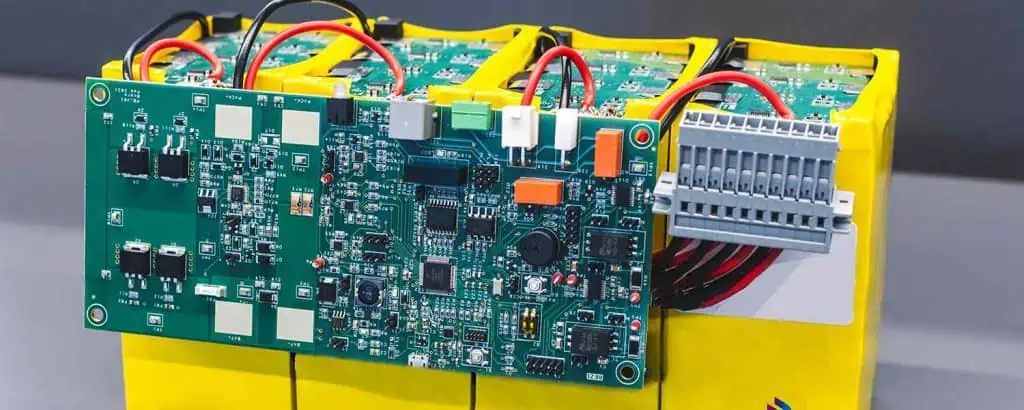
Battery Protection Circuit Design
Battery Thermal Management System
Protection circuits represent the last line of defense against battery failures:
Overvoltage Protection
Hardware cutoff: Circuits that physically disconnect the battery when voltage limits are exceeded
Analog comparators: Fast-acting voltage monitoring
Redundant monitoring: Multiple measurement points for reliability
Undervoltage Protection
Low-voltage cutoff: Preventing deep discharge damage
Hysteresis: Preventing oscillation around cutoff thresholds
Load disconnection: Circuits that isolate loads when voltage drops too low
Overcurrent and Short-Circuit Protection
Fast-acting fuses: Physical disconnection during serious faults
Current-sense resistors: Precise current monitoring
Reaction time optimization: Balancing false positives with adequate protection
Regulatory Compliance and Standards
Battery PCBs must comply with numerous standards and regulations:
Key Standards and Certifications
IEC 62133: Safety requirements for portable batteries
UL 1642: Standard for lithium batteries
UN 38.3: Transport testing requirements
ISO 26262: Functional safety for automotive applications
IPC-2221: PCB design standards
EMC/EMI Compliance
Battery PCBs must not generate or be susceptible to electromagnetic interference:
EMI filtering: Preventing noise from affecting other systems
Shielding: Protecting sensitive circuits from external interference
Ground plane design: Minimizing ground loops and common-mode noise
Common Mistakes to Avoid in Battery PCB Design
Battery Circuit Diagrams
Even experienced designers can make critical errors in Battery PCB design:
Underestimating thermal challenges: Failing to account for worst-case temperature scenarios
Inadequate current handling: Undersizing traces or connectors
Poor component selection: Choosing parts that don’t meet the application requirements
Neglecting balancing circuits: Critical for multi-cell battery longevity
Ignoring firmware/software integration: Leaving security vulnerabilities or control issues
Insufficient testing: Not validating designs under all operating conditions
Future Trends in Battery PCB Design
Battery PCB technology continues to evolve rapidly:
Smart battery systems: Integration of AI for predictive diagnostics and adaptive charging
Wireless power management: Contactless charging and monitoring capabilities
Advanced materials: Graphene-enhanced PCBs for superior thermal and electrical performance
Flexible PCBs: Conforming to unique form factors for wearable devices
Integration with energy harvesting: Combining battery power with renewable energy sources
Conclusion
Battery PCB design represents a critical intersection of electrical engineering, safety engineering, and power management. As battery technologies continue to advance and applications demand more power in smaller packages, the importance of well-designed Battery PCBs will only increase.
Creating an effective Battery PCB requires balancing competing requirements: safety must never be compromised, yet efficiency and performance remain essential for commercial viability. By following the best practices outlined in this guide and staying current with evolving standards and technologies, designers can create Battery PCBs that deliver safe, efficient, and high-performing battery systems.
Remember, the quality of a Battery PCB design directly impacts not only the performance of the device it powers but also the safety of its users. Investing in proper design, quality components, and thorough testing is essential for creating battery systems that can be trusted in an increasingly battery-powered world.
FAQs About Battery PCB Design
Q: What is the most critical factor in Battery PCB design? A: Safety is the most critical factor. A well-designed Battery PCB must prioritize protection against thermal runaway, overcharging, and short circuits to prevent potentially dangerous failures.
Q: How do Battery PCBs extend battery life? A: Battery PCBs extend battery life through precise charge management, cell balancing in multi-cell configurations, temperature monitoring, and preventing deep discharge conditions.
Q: What’s the difference between passive and active cell balancing? A: Passive balancing dissipates excess energy from higher-charged cells through resistors, while active balancing transfers energy from higher-charged cells to lower-charged cells, resulting in better efficiency but greater circuit complexity.
Q: How do Battery PCBs handle thermal management? A: Battery PCBs manage thermal challenges through strategic component placement, copper pours for heat dissipation, thermal vias to transfer heat between layers, and temperature monitoring circuits that can reduce current or shut down the system when temperatures exceed safe limits.
Q: What standards should Battery PCB designers be familiar with? A: Designers should be familiar with IEC 62133 for portable battery safety, UL 1642 for lithium batteries, UN 38.3 for transport requirements, and applicable industry-specific standards like ISO 26262 for automotive applications.
In the world of printed circuit boards (PCBs), color plays a more significant role than you might think. While green has long been the standard color for PCBs, blue PCBs have gained popularity in recent years. This article will explore the reasons behind the use of blue solder mask on PCBs, its advantages, and when you should consider using it for your projects.
Understanding Solder Mask Colors
Before we dive into the specifics of blue PCBs, let’s first understand what solder mask is and why color matters in PCB manufacturing.
What is Solder Mask?
Solder mask is a thin layer of polymer applied to the copper traces of a PCB. Its primary functions include:
Protecting copper traces from oxidation
Preventing solder bridges between closely spaced solder pads
Improving the board’s appearance and readability
Shielding the board from environmental factors
The Significance of Solder Mask Color
While the color of the solder mask doesn’t directly affect the PCB’s electrical performance, it can impact various aspects of the manufacturing process and the board’s usability. Common solder mask colors include:
Green (traditional and most common)
Blue
Red
Black
White
Yellow
Each color has its own set of advantages and use cases, with blue PCBs becoming increasingly popular for specific applications.
The Rise of Blue PCBs
Blue PCBs have gained traction in the electronics industry for several compelling reasons. Let’s explore why manufacturers and designers are increasingly opting for blue solder mask.
Aesthetic Appeal
One of the primary reasons for choosing a blue PCB is its aesthetic appeal. The vibrant blue color gives the board a modern, high-tech appearance that can be particularly attractive in consumer electronics or showcase projects.
Improved Contrast and Visibility
Blue solder mask provides excellent contrast against copper traces and white silkscreen printing. This high contrast can make it easier to:
Inspect the board for defects
Read component labels and markings
Identify trace patterns and board features
Color Psychology and Branding
The color blue is often associated with trust, professionalism, and technology. Using blue PCBs can subtly reinforce these qualities in your products, potentially influencing customer perception and enhancing brand identity.
Reduced likelihood of defective boards reaching end-users
2. Better Photographic Documentation
When documenting PCB designs or creating marketing materials, blue PCBs tend to photograph well. The blue background provides a clean, professional look that can enhance:
Technical documentation
Marketing materials
Online product listings
3. Reduced Eye Strain
For engineers and technicians who spend long hours working with PCBs, the blue color can be less straining on the eyes compared to the traditional green. This can potentially lead to:
Increased productivity
Reduced fatigue during long work sessions
Fewer errors in manual assembly or rework processes
4. Differentiation in Multi-Board Systems
In systems that use multiple PCBs, using blue boards can help differentiate between different board types or revisions. This can be particularly useful in:
Prototype development
Version control
Assembly and maintenance of complex systems
5. UV Protection
Some blue solder masks offer improved UV resistance compared to other colors. This can be beneficial for PCBs used in:
Outdoor applications
UV-intense environments
Long-term exposure to sunlight
When to Use Blue PCBs
While blue PCBs offer several advantages, they may not be the best choice for every application. Here are some scenarios where using a blue PCB might be particularly beneficial:
1. High-End Consumer Electronics
For premium consumer electronics where aesthetics matter, blue PCBs can add a touch of sophistication and visual appeal. Consider using blue PCBs in:
Blue PCBs can be excellent for prototype and development boards, where clarity and ease of inspection are crucial. They’re particularly useful for:
Educational kits
Open-source hardware projects
Rapid prototyping in R&D environments
3. Medical Devices
In medical equipment, where cleanliness and precision are paramount, blue PCBs can provide a perceived sense of hygiene and accuracy. Consider blue PCBs for:
In industrial settings where PCBs may be exposed to harsh environments, the UV-resistant properties of some blue solder masks can be advantageous. Consider blue PCBs for:
Factory automation equipment
Outdoor control panels
Marine electronics
Considerations When Choosing Blue PCBs
While blue PCBs offer numerous benefits, there are some factors to consider before making the switch:
1. Cost Implications
Blue solder mask may be slightly more expensive than traditional green, especially for small production runs. Consider whether the benefits outweigh the potential cost increase.
2. Availability and Lead Times
Some PCB manufacturers may have longer lead times or limited availability for blue solder mask. Check with your supplier about any potential delays.
3. Regulatory Compliance
In some industries, there may be specific color requirements for PCBs. Ensure that using a blue PCB doesn’t conflict with any regulatory standards in your field.
4. Thermal Considerations
Different solder mask colors can have varying thermal properties. If your application involves high-power components or extreme temperatures, consult with your PCB manufacturer about the thermal characteristics of their blue solder mask.
5. Consistency Across Batches
Color consistency can vary between manufacturers and even between production batches. If color uniformity is crucial for your application, discuss this with your PCB supplier.
Best Practices for Using Blue PCBs
If you decide to use blue PCBs in your projects, consider these best practices to maximize their benefits:
1. Optimize Silkscreen Color
Choose a silkscreen color that provides maximum contrast against the blue background. White is often the best choice, but yellow or light gray can also work well.
2. Consider Component Colors
When selecting components, consider how their colors will look against the blue background. This can enhance the overall aesthetic appeal of your board.
3. Leverage Contrasting Colors for Test Points
Use contrasting colors for test points or important markers on the board to make them easily identifiable during testing and assembly.
4. Maintain Consistent Lighting
Since the appearance of blue PCBs can vary under different lighting conditions, try to maintain consistent lighting in your inspection and assembly areas.
5. Educate Your Team
If your team is used to working with green PCBs, provide training on any specific considerations or best practices for working with blue boards.
Conclusion
Blue PCBs offer a range of benefits, from improved visibility and inspection capabilities to enhanced aesthetic appeal and potential UV resistance. While they may not be the best choice for every application, blue PCBs can be an excellent option for high-end consumer electronics, prototypes, medical devices, and certain industrial applications.
When considering whether to use blue PCBs, weigh the advantages against factors such as cost, availability, and regulatory requirements. By carefully evaluating your specific needs and following best practices, you can leverage the benefits of blue PCBs to enhance both the form and function of your electronic designs.
As the electronics industry continues to evolve, the choice of PCB color is becoming an increasingly important aspect of product design. Whether you’re developing cutting-edge consumer technology or high-reliability industrial systems, blue PCBs offer a compelling option that combines practicality with visual appeal.
The importance of circuit boards to the functionality of electronics cannot get stated enough. It ensures proper mechanical and electrical signaling within the circuit. However, circuit boards come in many forms and types, and it cannot surprise me if you have never heard of a button PCB. The PCB comes as an uncommon type, complete with a circuit board button. Therefore, if you love circuit boards, perhaps it would do you some good to dig and understand this printed circuit board.
The Button Printed Circuit Board
Button PCBs have widespread application, and perhaps because of the simplicity of their application, not many people know how often they interact with them. The simple yet effective PCB button pad example includes everyone inadvertently using a remote control device. Rings a bell now? A button PCB contains a markedly visible coil pattern, all crucial single-layer PCB components, but besides these, it also possesses buttons to complete or break circuits.
Many individuals, including experienced PCB designers and manufacturers, often prove unaware of how a button-printed circuit board works. To understand this, imagine a product with the capacity to sense and react to the immediate surrounding. Such a product will need the correct components to make it operational. If this product involved a circuit board, then one of these key components would become a switch.
Switches come under two categories of “off” or “on.” The “off” implies that you must turn the switch “on” while the “on” switch always stays in a single mode. PCB buttons, therefore, get inferred as on/off switches. Consequently, such a printed circuit board gets referred to as a power button PCB.
A button PCB proves popular for electronic projects, primarily as a PCB layout. The component layout of such a PCB layout gets deployed in the fabrication of buttons. Therefore, you should not get surprised to discover its importance in controlling the digital touch knob. It uses a simple pushbutton to key in data when pressed and uses a LED matrix in displaying information.
A button PCB contains diverse features, including multiple interface types that allow it to get powered off or on, resetting it, or determining anything else you need to perform. It also contains four LEDs that prove programmable, where you can program them with different colors besides timing restrictions.
The Button PCB has many different features, including multiple interfaces that enable the user to turn it on or off, reset it, or generally determine what they want it to do. The Button PCB also has four LEDs (light-emitting diodes) that can be programmed with different colors and timing restrictions for RGB lighting effects.
A button PCB comes as a small and standard circuit equipped with a power supply system that accepts wall adapters and batteries when it comes to powering your device. Therefore, it got developed to allow individuals to deploy them for their additional circuitry needs and personal use. Moreover, since a button PCB programming process proves simple, it acts as an incredible device for learning and prototyping circuits without investing further.
Here, it becomes instrumental in plugging the device into a button PCB before connecting the wires emanating from your power cables to each input pin. For powering low-voltage devices such as the sine wave, deploy a single wire for every button. However, if you have to power high-power devices, then dual (two) have to get fixed to each button. For instance, if you have three wires for powering the RGB LED strips, you should use two of the wires for the “on” and a single one for the “off” button. The outcome will encompass cutting off the power to a selected device when you get to press that button. Consequently, it makes the automation of homes easy while computer hacking also becomes more convenient. For instance, you can decide to program your home’s button PCB to switch on the lights when you leave the house and back on when you enter.
PCB touch button and socket
The pcb touch button, which is usually completely encapsulated in a plastic case, contains the actual electronics and controls the button’s opening and closing action. The pcb touch button can be used as a standard button. It can also be configured to produce customized clicks via embedded software. The contacts that plug into your device are often located at or near the bottom of the PCB. This is due to how shallow the PCB’s cavity is in order to maximize area for the touch button and minimize space needed for its components. This means that the buttons are laid out in a way that makes them easier to manufacture or assemble.
Vital Terminologies Used in Button PCB
Circuit board button. It represents a modest circuit that comprises limited components like the LED, button, and resistor R1. Some instances see an IC (integrated circuit) which acts as the circuit controller. A controller gets deployed as a blend with further circuits and printed circuit boards that it regulates. You can connect components to the PCB or opt to solder them. Whenever you press the PCB button, you short-circuit the IC pins and trigger specific responses. Upon release, the integrated circuit pin connection breaks, and therefore it will no longer respond.
It also becomes crucial to present some vital concepts like the touchpad, power supply pin, and a PE circuit. If you use these concepts, designing a stable printed circuit board with an enhanced outcome becomes a reality.
Printed-electrolysis circuit (PE). It is a circuit that gets primarily used to supply power to your button pad. It often proves concealed between the copper plate and the silicon rubber. The PE utilizes the electrolysis in generating the 5V power via the copper and other elements (chemical) contained around that spot. Therefore, you have no cause to stress about proving an unknown quantity as its operation proves simple to comprehend. Additionally, it is similar to other chemical reactions.
The power supply pin. It comes as two copper pads, with one acting as the ground and the other the positive. The pads are located in the middle of the printed circuit board. It functions as power supply conduits to the integrated circuit or BP (button pad). However, it also becomes necessary to avoid confusing the pins with the GND connection as they possess a lower voltage compared to normal PCB buttons. Therefore, you cannot deploy it to supply power by connecting it to the IC directly. Consequently, the existence of a PE circuit becomes essential, especially in dealing with this challenge.
Touchpad. It becomes essential to get familiar with touchpads, especially after building a printed circuit board. A touchpad denotes the area responsible for sensing any finger touch. The area gets isolated from other adjoining areas (from 50% to 100%) to provide an almost zero parasitic capacitance. It is for this reason that it gets inferred to as the touchpad. Typical touchpads come as one-layer, two-layer, and three-layer printed circuit boards, with diverse characteristics.
It becomes crucial to avoid creating the circuit for your touchpad, especially if you make printed circuit boards. The reason lies in the complexity involved. For instance, placing plenty of capacitors on a parallel arrangement will lead to an incidence of parasitic capacitance, where these tally up fast to create a high-impendence input (where the capacitors turn into equals with one another). Consequently, your printed circuit board will end up malfunctioning. It proves a typical problem that most people experience with their circuits as it becomes stuck)
As an astute PCB designer, it becomes crucial to comprehend a PCBA’s power supply pin well. It will help you avoid the prevalence of working with unstable PCBs. Additionally, the highly-impedance touchpads demand careful consideration from you.
However, if you cannot go about this the correct way, then it will become ideal to contact and outsource the services of RayMing PCB and Assembly Company to create such a complex touchpad for you. You will get quality guidelines on the ordering process on their website and get a fair deal within a reasonable time. What’s more? You will get excellent customer service as you await your touchpad circuit.
In short, it becomes instrumental in understanding everything concerning PE circuits besides the power supply pin contained in PCBs, especially for people who yearn to design and handle printed circuit boards. You then have to design your intended signal output in line with the relevant rules to ensure you keep it stand and working every time.
In the article, we have enclosed some elementary details concerning the button-printed circuit boards and, by extension, the PCB industry. We have shared all the necessary details to understand some typical challenges predominant in the world of button boards. Therefore, if you hold an interest in making your design, do not fail to focus on these crucial points. Additionally, if you have questions, you can always visit RayMing PCB and Assembly company website to get more details about printed circuit boards, procuring these services and products, and understanding circuits in general. Happy reading.
In the ever-evolving world of electronics, Printed Circuit Boards (PCBs) serve as the backbone of countless devices, from smartphones to industrial machinery. Understanding PCB pricing is crucial for anyone involved in electronics development, from startup entrepreneurs to established manufacturers. The cost of PCBs can significantly impact product design decisions, prototyping processes, and ultimately, the final manufacturing cost of electronic devices.
This comprehensive guide delves into the multifaceted world of PCB pricing, exploring the various factors that influence costs from the initial prototype stage to large-scale production runs. By gaining insight into these factors, designers, engineers, and project managers can make informed decisions that balance quality, performance, and cost-effectiveness in their PCB projects.
A Printed Circuit Board (PCB) is a fundamental component in electronic devices, providing mechanical support and electrical connections for electronic components. PCBs consist of conductive pathways, tracks, or signal traces etched from copper sheets laminated onto a non-conductive substrate.
1.2 Why PCB Cost Matters
Understanding PCB pricing is crucial for several reasons:
For startups: Every dollar counts, and optimizing PCB costs can make or break a product’s viability.
For large companies: Even small savings per unit can translate to significant amounts when producing millions of boards.
For all businesses: Balancing cost with quality and performance is key to staying competitive in the electronics market.
1.3 Key Terms to Know
Prototype: Initial PCB version for testing and validation.
Batch Production: Manufacturing PCBs in small to medium quantities.
PCB Assembly (PCBA): The process of soldering components onto a bare PCB.
Minimum Order Quantity (MOQ): The smallest number of PCBs a manufacturer will produce in a single order.
2. Core Factors Affecting PCB Pricing
2.1 Material Costs
The choice of PCB material significantly impacts the overall cost. Common materials include:
The impact of material choice on PCB board price and printed circuit board price can be substantial. For instance, a high-frequency Rogers material can cost 5-10 times more than standard FR4.
2.2 Board Size and Layer Count
Board dimensions and the number of layers directly affect the circuit board price:
Larger boards require more material and processing time.
Multi-layer boards are more complex to manufacture than single or double-sided boards.
Cost differences based on layer count:
Single-layer: Base cost
Double-layer: ~1.5x to 2x single-layer cost
4-layer: ~2.5x to 3x double-layer cost
6-layer and above: Increases exponentially
2.3 Production Volume
The relationship between production volume and PCB cost per unit is inversely proportional:
Prototypes and small batches have higher per-unit costs due to setup fees and lower efficiency.
Bulk orders benefit from economies of scale, reducing per-unit costs significantly.
Minimum Order Quantity (MOQ) also plays a role in pricing. Manufacturers often offer better rates for orders meeting or exceeding their MOQ.
2.4 PCB Complexity
Several factors contribute to PCB complexity and, consequently, to the price:
Via Types:
Through-hole: Lowest cost
Blind vias: Moderate increase in cost
Buried vias: Highest cost due to additional manufacturing steps
The decision to purchase PCB manufacturing equipment depends on production volume, required capabilities, and long-term cost analysis compared to outsourcing.
Combine multiple designs on a single panel to reduce setup costs
Select appropriate specifications:
Don’t over-specify tolerances or materials beyond what’s necessary
Consider lead-free options only when required
6.2 Comparing Quotes from Multiple Manufacturers
Request quotes from at least 3-5 manufacturers
Compare not just price, but also quality, lead time, and customer service
Consider the total cost of ownership, including potential rework or quality issues
6.3 Understanding Hidden Fees
Be aware of additional costs that may not be immediately apparent:
Shipping fees, especially for international orders
Tooling charges for custom designs or non-standard features
Testing and inspection fees for high-reliability applications
7. Future Trends in PCB Pricing
7.1 Automated Manufacturing and Smart Factories
The increasing adoption of Industry 4.0 technologies in PCB manufacturing is likely to impact pricing:
Potential for lower costs due to increased efficiency and reduced labor
Higher initial investment in equipment may temporarily increase prices
More consistent quality could reduce overall project costs by minimizing rework
7.2 Impact of Material Shortages and Global Supply Chains
Recent global events have highlighted the volatility of supply chains:
Material shortages can lead to price fluctuations and longer lead times
Diversification of supply chains may increase resilience but potentially at a higher cost
Localized production might become more prevalent, affecting pricing structures
7.3 Innovations in PCB Recycling and Eco-friendly PCBs
As sustainability becomes a greater focus:
Development of more easily recyclable PCB materials could impact pricing
Potential for regulations on PCB disposal to affect overall project costs
Market demand for eco-friendly electronics may drive innovation in PCB materials and processes
Conclusion
Understanding the multifaceted nature of PCB pricing is crucial for anyone involved in electronics development and manufacturing. From material selection and board complexity to production volume and turnaround time, numerous factors influence the final cost of a PCB project.
Key takeaways for managing PCB costs effectively:
Carefully consider design choices and their impact on manufacturability and cost.
Balance quality requirements with budget constraints to avoid over-engineering.
Plan strategically from prototyping to mass production, considering long-term costs and scalability.
Stay informed about industry trends and technological advancements that may affect PCB pricing in the future.
By applying the insights from this guide, electronics professionals can make informed decisions that optimize PCB costs without compromising on quality or performance. As the electronics industry continues to evolve, staying adaptable and knowledgeable about PCB pricing factors will remain crucial for success in this dynamic field.
In the world of electronics manufacturing, the choice of Printed Circuit Board (PCB) color is more than just an aesthetic decision. While green PCBs have long been the industry standard, black PCBs are gaining popularity for their unique advantages. This article delves into the world of black PCBs, exploring their benefits, applications, and why they might be the right choice for your next electronic project.
1. Introduction to Black PCBs
1.1 What is a Black PCB?
A black PCB is a printed circuit board that uses a black solder mask instead of the traditional green. The solder mask is the thin layer of polymer that covers the copper traces on a PCB, protecting them from oxidation and preventing solder bridges during assembly.
1.2 The Rise of Black PCBs
In recent years, black PCBs have seen a surge in popularity, particularly in high-end consumer electronics, automotive applications, and specialized industrial equipment. This trend is driven by both aesthetic and functional considerations.
2. Advantages of Black PCBs
Black PCBs offer several distinct advantages over their green counterparts, making them an attractive option for many applications.
2.1 Enhanced Heat Dissipation
One of the most significant benefits of black PCBs is their superior heat dissipation properties. The black color absorbs and radiates heat more effectively than lighter colors, potentially leading to better thermal management in electronic devices.
2.2 Improved Contrast for Inspection
Black solder mask provides excellent contrast against copper traces, component markings, and solder joints. This high contrast makes visual inspection easier and more accurate, potentially reducing assembly errors and improving quality control processes.
2.3 Aesthetic Appeal
In an era where product design is increasingly important, black PCBs offer a sleek, modern appearance. This can be particularly valuable in consumer electronics where the PCB might be visible through transparent or translucent casings.
2.4 Reduced Light Reflection
Black PCBs reflect less light than their lighter-colored counterparts. This property can be crucial in applications where stray light reflection could interfere with optical sensors or other light-sensitive components.
2.5 Enhanced Durability
Some manufacturers claim that black solder mask can offer improved durability and resistance to environmental factors compared to traditional green solder mask.
The unique properties of black PCBs make them suitable for a wide range of applications across various industries.
3.1 Consumer Electronics
High-end smartphones, laptops, and gaming consoles often use black PCBs for their aesthetic appeal and thermal properties.
3.2 Automotive Electronics
The automotive industry is increasingly adopting black PCBs in dashboard displays, infotainment systems, and under-hood electronics due to their heat dissipation properties and durability.
3.3 Aerospace and Defense
Black PCBs are finding applications in aerospace and defense equipment, where their heat management properties and reduced light reflection can be advantageous.
3.4 Industrial Control Systems
In industrial settings, black PCBs are used in control systems and monitoring equipment, where their ease of inspection and durability are valuable assets.
3.5 LED Lighting
The heat dissipation properties of black PCBs make them an excellent choice for LED lighting applications, particularly in high-power or compact designs.
4. Manufacturing Process of Black PCBs
The manufacturing process for black PCBs is similar to that of traditional PCBs, with a few key differences.
4.1 Material Selection
The base material for black PCBs is typically the same as for other PCBs, usually FR-4 (a glass-reinforced epoxy laminate). The key difference lies in the solder mask.
4.2 Solder Mask Application
The black solder mask is applied using similar techniques to green solder mask, such as screen printing or photoimaging. However, achieving a uniform, deep black color can be more challenging and may require specialized formulations.
4.3 Curing Process
After application, the black solder mask undergoes a curing process, typically involving UV exposure and heat treatment. This process may need to be carefully controlled to ensure the desired color and properties are achieved.
4.4 Quality Control
Quality control for black PCBs may involve additional steps to ensure color consistency and check for any defects that might be more visible against the black background.
5. Challenges and Considerations
While black PCBs offer many advantages, there are also some challenges and considerations to keep in mind.
5.1 Cost Implications
Black PCBs may come at a premium compared to traditional green PCBs due to the specialized materials and potential additional processing steps required.
5.2 Heat Absorption in Certain Environments
While the heat dissipation properties of black PCBs can be advantageous, in some environments, the increased heat absorption could potentially lead to higher operating temperatures if not properly managed.
5.3 Visibility of Certain Components
Some components or markings might be less visible against a black background, potentially requiring adjustments in assembly or inspection processes.
5.4 Limited Availability
Not all PCB manufacturers offer black solder mask options, which could limit sourcing options for some projects.
6. Black PCBs vs. Traditional Green PCBs
To fully appreciate the impact of black PCBs, it’s essential to compare them directly with traditional green PCBs.
6.1 Thermal Performance
Black PCBs generally offer better heat dissipation compared to green PCBs, which can be crucial in high-power or compact designs.
6.2 Visual Inspection and Assembly
The high contrast provided by black PCBs can make visual inspection easier compared to green PCBs. However, this may vary depending on the specific components and markings used.
6.3 Aesthetic Considerations
Black PCBs offer a more modern, sleek appearance compared to the traditional look of green PCBs. This can be a significant factor in consumer electronics and other visible applications.
6.4 Cost Comparison
Black PCBs typically come at a higher cost compared to green PCBs due to the specialized materials and potential additional processing steps.
6.5 Industry Adoption
While green PCBs still dominate the market, black PCBs are gaining ground, especially in specific sectors like high-end consumer electronics and automotive applications.
7. Future Trends in Black PCB Technology
The future of black PCB technology looks promising, with several emerging trends:
7.1 Advanced Materials
Research is ongoing to develop black solder mask materials with improved properties, such as enhanced thermal conductivity and durability.
7.2 Integration with Flexible and Rigid-Flex PCBs
As flexible and rigid-flex PCBs become more prevalent, we can expect to see black solder mask options for these advanced board types.
7.3 Improved Manufacturing Processes
Advancements in manufacturing processes may lead to more consistent and cost-effective production of black PCBs.
7.4 Customization and Branding Opportunities
The use of black PCBs may open up new possibilities for customization and branding, such as laser etching or printing vibrant colors on the black background.
7.5 Sustainability Considerations
Future developments may focus on creating more environmentally friendly black solder mask materials, aligning with the growing emphasis on sustainability in electronics manufacturing.
8. Choosing Between Black and Green PCBs
When deciding between black and green PCBs for your project, consider the following factors:
8.1 Application Requirements
Consider the specific requirements of your application, such as thermal management, light reflection, and visibility needs.
8.2 Design Aesthetics
If the PCB will be visible in the final product, the aesthetic appeal of black PCBs might be a deciding factor.
8.3 Budget Constraints
Weigh the potential benefits of black PCBs against their higher cost to determine if they fit within your project budget.
8.4 Manufacturing Capabilities
Ensure that your chosen manufacturer has experience and capabilities in producing high-quality black PCBs.
8.5 Industry Standards and Expectations
Consider any industry-specific standards or expectations that might influence the choice between black and green PCBs.
Conclusion
Black PCBs represent an exciting development in the world of electronics manufacturing. Their unique properties, including enhanced heat dissipation, improved contrast for inspection, and aesthetic appeal, make them an attractive option for a wide range of applications. While challenges exist, such as higher costs and potential limitations in certain environments, the benefits of black PCBs often outweigh these considerations in many modern electronic designs.
As technology continues to advance and the demand for high-performance, visually appealing electronics grows, we can expect to see further innovations in black PCB technology. Whether you’re designing cutting-edge consumer electronics, robust industrial control systems, or next-generation automotive components, black PCBs offer a compelling alternative to traditional green boards.
Ultimately, the choice between black and green PCBs will depend on the specific requirements of your project. By carefully considering the advantages, challenges, and future trends associated with black PCBs, you can make an informed decision that balances performance, aesthetics, and cost-effectiveness in your electronic designs.
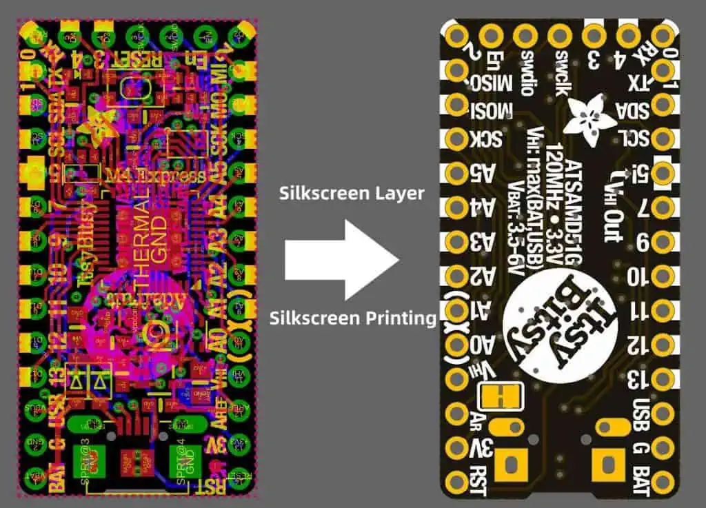
The silkscreen, also known as the soldermask legend, is the layer of printed text, markings, and graphics on the surface of a printed circuit board (PCB) that identifies components, displays text, and provides reference markers for manufacturing and assembly. This article provides a comprehensive overview of PCB silkscreen including its purposes, printing process, design, applications, and considerations.
Definition of a PCB Silkscreen
The silkscreen refers to the topmost layer on a PCB consisting of text, component outlines, fiducials, logos, and other graphics printed in ink. It takes its name from the fabric mesh historically used in the printing process. Silkscreening allows marking non-conductive areas of the PCB surface.
Modern silkscreens utilize advanced print, photoresist, and laser direct imaging techniques.
Purposes of Silkscreen
Key roles that the silkscreen serves:
Component Identifiers – Names, designators, values for placement and assembly
Component Outlines – Displays footprint outlines for BGAs etc.
Board Information – Title, revision, manufacturer data
Logo and Text – Company branding information
Special Markings – Date code, copyrights, approvals
Cracking – Thermal expansion mismatch with substrate
Adequate silkscreen thickness reduces damage risks. But expect some degradation over product lifetime.
Silkscreen Repair and Rework
Damaged silkscreens can be repaired:
Touch Up – Using matching pen or paint
Printed Overlay – Adhesive legend printed on transparent film
Full Replacement – Strip and reprint defective areas
Scraping – Removing damaged silkscreen section
But rework is often easier with liquid photoimageable legend.
Silkscreen vs Laser Engraving
Laser engraving directly marks the substrate as an alternative to silkscreen:
Silkscreen
Ink-based, masks required
Fine features, high durability
Lower cost
Laser Engraving
Direct ablation marking
Simpler process, no chemicals
Crisp text even on BGAs
Only marks surface
Silkscreen vs Inkjet Printing
Inkjet printers offer moderate print resolution:
Silkscreen
Higher durability and longevity
Fine pitch capability
Lower running cost at volume
Inkjet Printing
Eliminates screens and chemicals
Simpler graphics changes
Only short production runs
Automated Optical Legend Inspection
Automated tools like AOI systems check silkscreen quality:
Verifies text legibility and print quality
Checks location and alignment to copper
Confirms all required markings are present
Comparators check against golden board
Can detect defects down to 0.15mm
This automation speeds inspection, improving quality.
Conclusion
The silkscreen legend fulfills a wide variety of invaluable marking, identification, and display purposes on PCB assemblies. As PCBs grow more complex, silkscreens must condense more information into less space while maintaining durability. Fortunately, continued advancements in printing technology empower PCB designers to incorporate high value visual aids without compromising on miniaturization and performance. The humble silkscreen remains a key asset in manufacturing, inspecting, assembling, operating, and servicing virtually all modern electronics hardware.
FAQs
Q: What other names refer to the PCB silkscreen?
A: Common synonyms are solder mask legend, photoimageable legend, screen print, and solder resist legend.
Q: What printing methods allow the smallest silkscreen text?
A: Both liquid photoimageable and dry film printing support text below 1mm for high density designs.
Q: Does silkscreen ink contain lead or other hazardous substances?
A: Most legend inks today are lead-free and RoHS compliant. Some risk exists with older PCB stocks.
Q: Can conductive inks be printed on the silkscreen layer?
A: Yes, using specialty conductive inks, warnings and symbols can be printed within the silkscreen.
Q: Does silkscreen ink withstand soldering heat?
A: Thermally cured legend inks are designed to resist typical soldering, though some degradation can occur over repeated reflow exposure.
How to elegantly arrange PCB silkscreen
PCB silkscreen printing is the use of screen printing technology to make printed circuit boards. The silk screen value is the silk screen layer. When drawing the pcb layer. The layer containing the text legend is used to mark components or add other information. This layer is called the silk screen layer.
The component shape, serial number, and other descriptive text are printed on the component surface or solder surface by screen printing to facilitate the plug-in (including the surface-mounted component patch) of the circuit board production process and the maintenance operation of the product in the future.
The PCB silk screen layer is generally placed on the top layer (Top), but for the electronic products with high failure rate and frequent maintenance, such as the motherboard of TVs, computer monitors, printers, etc., the silk screen layer can be set on the component side and the soldering surface. .
Many PCB engineers who draw PCB think that silkscreen does not affect the performance of the circuit, so it does not pay attention to silkscreen. However, for a professional hardware engineer, you must pay attention to these details.
The following describes the method of elegantly arranging PCB silkscreen.
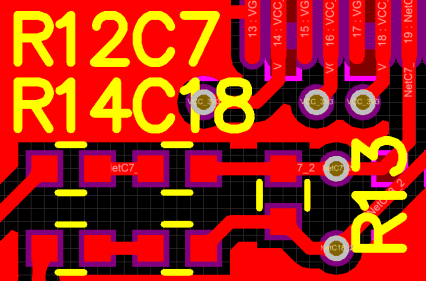
1.Placement area
In general, the silkscreen printing of resistors, capacitors, tubes, etc., do not use four directions when placing, this will lead to debugging, repair, welding, see silk screen is very tired (the board has to turn several directions) .
Therefore, it is recommended to place it in two directions at most, as shown in the figure below. This way, it will be very convenient to view the silk screen.
As shown in the figure below, if the components are too dense, and you can’t put on the silk screen, you can write a silk screen in the blank place nearby, mark the arrow, and then draw a frame,which is convenient for identification.
As shown in the figure below, the via is on the silkscreen 8 . After the PCB is made, you will not know whether it is R48 or R49.
3、Do not Arrange the silkscreen on high speed signals(eg, clock lines, etc.).
This recommendation is for high speed signals on the top or bottom layer, because such signal circuit can be considered as microstrip lines.
The speed of the signal running on the microstrip line (phase velocity) is related to the medium. If the silk screen is pressed to the line, as shown in the figure below, the medium will become uneven, causing the phase velocity to change, and finally the impedance is discontinuous. , affecting signal quality.
Of course, there will be no such problem
with the signal line of the inner layer.
4、The reading direction of silkscreen should be consistent with the direction of use.
As shown in the figure below, the reading direction of the silkscreen is the same as the direction of use of the chip, mainly when welding, reducing the probability of the welding being reversed.
Others, such as electrolytic capacitors, may not follow this recommendation because you can indicate positive and negative polarity.
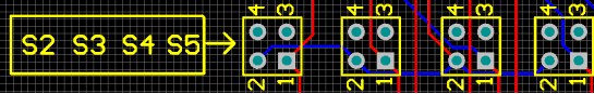
5、The pin number should be marked on the silkscreen.
As shown in the figure below, the P3 connector is marked with 4 pin numbers for easy debugging/installation. In addition, it is best to mark the pin-intensive places, such as chips, FPC sockets, etc.
At the same time, it also meets the previous recommendation. The reading direction of P3 is the same as the direction of use of the connector.
For special components such as BGA and QFN, the size of the silkscreen should be exactly the same as the size of the chip (as shown in the figure below). Otherwise, it will be difficult to align and affect the soldering.
7、Silkscreen of the mount hole
Here, the silk screen of the screw is added near the mounting hole, and the length and the total number of screws are marked for easy installation.
In the competitive world of electronics manufacturing, selecting the right PCB surface finish is crucial for ensuring product reliability, performance, and cost-effectiveness. Among the various options available, immersion silver PCB finish has gained significant popularity due to its unique properties and benefits. This comprehensive guide explores everything you need to know about immersion silver PCB finish, from its technical specifications and cost considerations to durability factors and manufacturing best practices.
Understanding Immersion Silver PCB Finish
What Is Immersion Silver PCB Finish?
Immersion silver (ImAg) is a popular surface finish option in PCB manufacturing that involves depositing a thin layer of pure silver onto exposed copper surfaces through a chemical displacement process. During this process, copper atoms on the board surface are replaced by silver atoms from the plating solution, creating a uniform silver coating typically ranging from 0.05 to 0.15 micrometers in thickness.
The immersion silver PCB finish creates a flat, planar surface with excellent electrical conductivity and solderability characteristics. Unlike some other finishes that involve multiple metal layers, immersion silver is a single-metal finish that forms a direct interface with the underlying copper.
The Chemical Process Behind Immersion Silver Plating
The immersion silver plating process is relatively straightforward but requires precise control of chemical parameters to achieve optimal results. The basic steps include:
Thorough cleaning of the copper surface to remove contaminants
Micro-etching to enhance adhesion
Pre-dip treatment to prepare the surface
Immersion in the silver plating solution where the displacement reaction occurs
Rinsing and anti-tarnish treatment to protect the fresh silver coating
This chemical displacement reaction is self-limiting, meaning once the copper surface is completely covered with silver, the reaction stops naturally. This self-limiting characteristic helps ensure uniformity across the entire board surface.
Immersion silver PCB finish offers excellent electrical conductivity, making it particularly valuable for high-frequency applications. The silver layer provides minimal signal loss and impedance control, which is crucial for RF circuits, high-speed digital designs, and other applications where signal integrity is paramount.
Outstanding Solderability
One of the primary advantages of immersion silver finish is its exceptional solderability. Fresh immersion silver surfaces exhibit near-perfect wetting characteristics with various solder alloys, creating reliable solder joints with minimal defects. This property is especially beneficial for fine-pitch components and complex assembly processes.
Planar Surface for Advanced Packaging
The immersion silver PCB finish produces a flat, uniform surface that’s ideal for advanced packaging technologies. This planar characteristic makes it particularly suitable for:
Fine-pitch components
Ball Grid Array (BGA) packages
Quad Flat No-leads (QFN) components
Other high-density interconnect technologies
The flatness ensures consistent contact across all connection points, reducing the risk of open connections or partial joints.
Environmental Compliance
Immersion silver PCB finish is fully RoHS and REACH compliant, containing no lead or other restricted substances. As environmental regulations continue to tighten globally, this compliance gives manufacturers peace of mind regarding regulatory requirements and sustainability goals.
Drawbacks and Considerations of Immersion Silver Finish
Susceptibility to Tarnishing
The most significant limitation of immersion silver PCB finish is its susceptibility to tarnishing and oxidation. When exposed to air, particularly in environments containing sulfur compounds, silver can tarnish relatively quickly, forming silver sulfide (Ag₂S). This tarnishing can affect solderability if not properly managed.
Several factors can accelerate the tarnishing process:
Presence of sulfur compounds (including those from cardboard packaging)
Fingerprint oils and other contaminants
Limited Shelf Life
Compared to alternative finishes like ENIG (Electroless Nickel Immersion Gold), immersion silver PCB finish has a shorter shelf life, typically ranging from 6 to 12 months under optimal storage conditions. Beyond this period, the solderability may start to deteriorate as the silver layer tarnishes.
Handling Sensitivity
Immersion silver requires careful handling throughout the manufacturing process. The silver surface is relatively soft and can be damaged by scratching or abrasion. Additionally, direct contact should be avoided as fingerprint oils can accelerate tarnishing in the contacted areas.
Immersion Silver vs. Other PCB Surface Finishes
Immersion Silver vs. ENIG
When comparing immersion silver PCB to ENIG (Electroless Nickel Immersion Gold), several key differences emerge:
While ENIG offers better longevity and corrosion resistance, immersion silver provides superior electrical performance and is more cost-effective for many applications.
Immersion Silver vs. HASL
Hot Air Solder Leveling (HASL) has been a traditional finish for decades, but immersion silver offers significant advantages in certain applications:
Aspect
Immersion Silver
HASL
Fine-pitch capability
Excellent
Poor
Surface planarity
Highly planar
Uneven (solder bumps)
Lead content
Lead-free
Can contain lead (leaded version)
Cost
Moderate
Lower (for leaded version)
Process complexity
Moderate
Higher (thermal stress)
Electrical performance
Excellent
Good
Immersion silver PCB finish is the clear winner for applications requiring fine-pitch components or planar surfaces, while HASL may still be preferred for less demanding, cost-sensitive applications.
Immersion Silver vs. OSP
Organic Solderability Preservative (OSP) is another popular lead-free option that competes with immersion silver:
Aspect
Immersion Silver
OSP
Multiple reflow capability
Good
Limited
Visual inspection
Easy (visible pads)
Difficult (transparent coating)
Electrical testing
Excellent
Challenging
Cost
Moderate
Lower
Environmental impact
Higher (silver waste)
Lower
Shelf life
6-12 months
3-6 months
OSP may be more economical, but immersion silver offers better electrical characteristics and easier testing and inspection capabilities.
Cost Analysis of Immersion Silver Finish
Typical Price Range
The cost of immersion silver PCB finish typically falls in the middle range compared to other surface finishes:
Approximately $0.10 to $0.25 per square inch premium over bare copper
For a standard 4-layer PCB design, immersion silver might add about 10-15% to the overall board cost compared to the most basic finishes.
Cost-Influencing Factors
Several factors can influence the final price of immersion silver PCB finish:
Board complexity: More complex designs with higher copper layer counts generally result in higher plating costs
Production volume: Larger production runs benefit from economies of scale
Board thickness: Thicker boards require more plating materials
Surface area ratio: The ratio of copper surface area to board size affects material usage
Quality requirements: Tighter specifications may require additional process controls
Geographic location: Manufacturing costs vary significantly by region
Total Cost of Ownership Considerations
When evaluating the cost-effectiveness of immersion silver PCB finish, manufacturers should consider the total cost of ownership, not just the initial plating cost:
Assembly yield: Superior solderability can reduce assembly defects and rework
Storage requirements: Special packaging may be needed to prevent premature tarnishing
Shelf life limitations: May lead to waste if production delays occur
Electrical performance: Higher signal integrity can reduce other design costs
The reliability and performance of immersion silver align well with the demanding requirements of automotive applications.
Medical Devices
Medical device manufacturers often select immersion silver PCB finish for critical applications:
Patient monitoring equipment
Diagnostic instruments
Imaging systems
Implantable device controllers
Laboratory automation equipment
The excellent electrical performance and RoHS compliance make immersion silver suitable for sensitive medical applications.
Conclusion
Immersion silver PCB finish offers an excellent balance of performance, cost, and manufacturability for many electronic applications. Its superior electrical characteristics, excellent solderability, and flat surface make it particularly valuable for high-frequency applications and fine-pitch assembly processes.
While it does require careful handling and has a more limited shelf life compared to some alternatives, these challenges can be effectively managed with proper procedures and controls. The cost-effectiveness of immersion silver makes it an attractive option for many manufacturers seeking to optimize their PCB production without the premium price of gold-based finishes.
For projects where signal integrity is critical, fine-pitch components are used, or environmental compliance is mandatory, immersion silver PCB finish should be a top consideration. As with any technical decision, consulting with experienced PCB manufacturers about your specific requirements will help ensure the best surface finish selection for your unique application.
Frequently Asked Questions
Is immersion silver PCB finish RoHS compliant?
Yes, immersion silver PCB finish is fully RoHS compliant as it contains no lead, mercury, cadmium, hexavalent chromium, PBB, or PBDE. It meets all requirements of the European Union’s Restriction of Hazardous Substances directive.
How does immersion silver compare to ENIG in terms of shelf life?
Immersion silver typically has a shorter shelf life (6-12 months) compared to ENIG (12+ months). This difference is primarily due to silver’s susceptibility to tarnishing when exposed to atmospheric sulfur compounds, while gold is highly resistant to oxidation and corrosion.
Can boards with immersion silver finish be reworked?
Yes, boards with immersion silver finish can be reworked, but care must be taken as each heating cycle can potentially degrade the finish. The silver layer is thin, and excessive heat or multiple rework cycles may completely consume the silver at solder joints. It’s advisable to use temperature-controlled equipment and minimize the number of rework cycles.
What causes the tarnishing of immersion silver finish?
Tarnishing of immersion silver is primarily caused by reaction with sulfur compounds in the atmosphere, forming silver sulfide (Ag₂S). Common sources of sulfur include air pollution, rubber materials, cardboard packaging, and even fingerprint oils. Humidity accelerates this reaction, as does higher temperature.
How thick is the immersion silver layer on a PCB?
The immersion silver layer on a PCB typically ranges from 0.05 to 0.15 micrometers (2-6 microinches) in thickness. This thin, uniform layer is sufficient to protect the underlying copper and provide excellent solderability while maintaining the dimensional precision required for fine-pitch components.
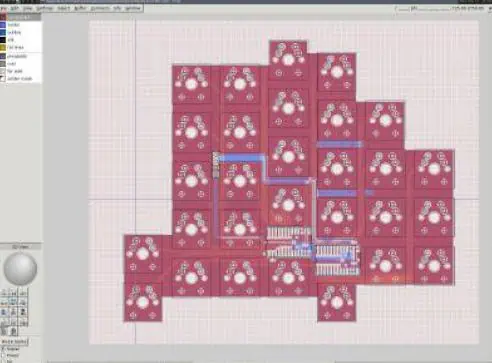
A keyboard PCB or printed circuit board is the physical platform that interconnects all the components in a computer keyboard. It plays a central role in transmitting key press inputs to the host computer. This article provides a comprehensive overview of keyboard PCB design, manufacturing, and functionality.
Keyboard PCB Basics
A keyboard PCB serves as the structural base to mount and connect the various components:
Switch matrix – allows detecting key presses
Microcontroller – scans matrix and sends key data
Stabilizers – for larger keys like spacebar
Additional chips – drives LEDs, RGB, macros etc.
Connectors – interfaces with computer
Components are soldered onto the PCB
The PCB is the backplane that routes signals between the microcontroller, switch matrix, and computer interface.
Allowing endless keyboard variations to suit any need or preference!
Applications
Keyboard PCBs are used in:
Computer keyboards – for desktop, laptop, servers
Peripherals – music, gaming, point of sale
Smart devices – tablets, smart TVs, appliances
Industrial controls and instrumentation
Modern keyboard PCB manufacturing enables cost effective, high quality, and customizable data input devices.
Pros and Cons
Advantages:
Allows compact, thin keyboard designs
Supports extensive customization
High reliability with quality components
Disadvantages:
Repairs often require full PCB replacement
Custom PCBs involve high NRE costs
Tight component spacing can limit modularity
Conclusion
In summary, a keyboard PCB provides the interconnect foundation for all components in a keyboard. Careful trace routing, switch matrix design, and noise control are required to ensure reliable performance. When combined with quality switches, firmware, and enclosures, keyboard PCBs enable the creation of high performance and customizable data input devices. The vast range of computer peripherals we use today are enabled by advanced PCB and electronic manufacturing capabilities.
FAQs
Q: What is the minimum number of layers required for a keyboard PCB?
A: Simple keyboard matrices can be implemented with a single PCB layer. 2-4 layers are more common for including ground planes or more complex routing.
Q: What interface is most modern keyboard PCBs designed for?
A: USB has become the standard keyboard interface supported on modern PCBs, replacing legacy PS/2 and serial interfaces.
Q: What is the role of diodes in a keyboard switch matrix?
A: Diodes prevent ghosting by blocking reverse currents when multiple keys are pressed simultaneously in a matrix.
Q: What is an example microcontroller used in keyboard PCBs?
A: Many keyboards use ATmega32U4 or ATmega328P from Microchip due to their built-in USB support and ample GPIO for matrix scanning.
Q: How are most keyboard PCBs fabricated and assembled?
A: The majority of keyboard PCB manufacturing utilizes SMT assembly with automated pick-and-place and reflow soldering for high volume production.
Definition of Keyboard PCB and Some of the Variants
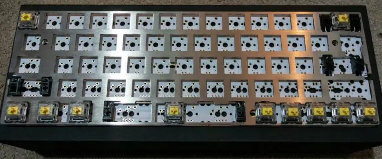
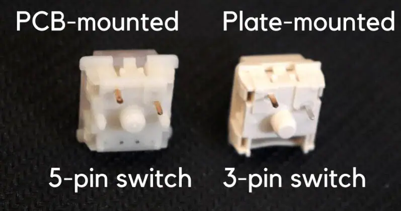
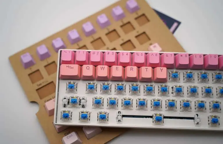
There are two mounting style types switches for mechanical keyboard: Plate mounted and PCB Mounted. Sorting out the distinction can be hard, so we’ll describe both switches more specific in this article. Plate-mounted switches only have 3 pins, in the other hand PCB-mounted switches have 5 pins. You can change PCB-mounted to fit with plate mounted switches by cutting the additional pins on the lower part of the switch. In this article, we’ll discuss entirely the contrast between these switches types and reveal to you how to adjust the switches to fit your board.
Fig. 1 PCB Mounted Switches vs Plate Mounted
The main difference between plate-mounted switch and PCB-mounted is the contact pins that they have. There are 3 pins on a plate-mounted switch, beside PCB-mounted has 5 pins.
Look closer at the bottom of PCB-mounted switches and you’ll find 5-pin switches in total. Those 5 pins are consist of two pins that is plastic based on the sides designed to give stability, two metal pins that make the switch working, and a “pin” at the center that looks more like an enormous round handle. By soldering the switches, it can be install to the PCB, and performing a simple mount as shown below.
Fig. 2 PCB-Mounted Switches Illustration
As for PCB-mounted switches, it also has guiding pins to help mount the switch on the PCB. Commonly, this kind of assembly has a lighter vibe, and the keys will might spring back a bit more. This mounting mostly utilized in a small size keyboard as they will need less construction to hold and have less flexibility. Nonetheless, in the current board, having a plate is extremely normal. It is feasible to decide to assemble a keyboard which do not have a plate, soldering quality will determine the switch stability.
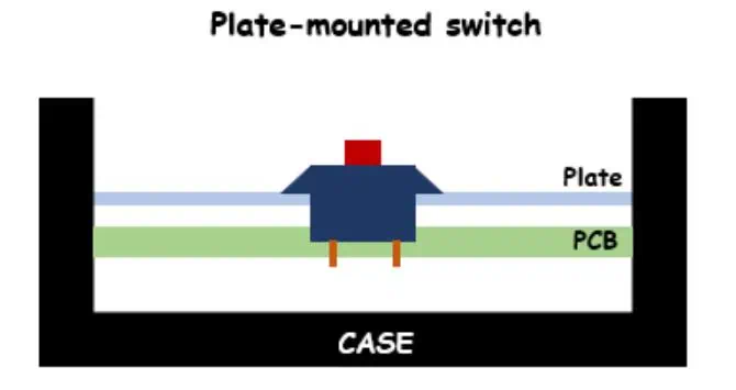
Plate Mounted Switch .The fact that these switches require a plate hence it is called Plate-mounted switches. Only 3 pins exist on the base: the center round knob and the two metal pins. It is designed with the plate because they do not have the stabilization pins. Each switch will be stabilized by the plate and decrease side-to-side staggering no matter when the key is pushed down (as demonstrated beneath).
As for Plate-mounting, it needs to install the switches with a metal plate which is located over the PCB. Then soldered the switches to the PCB after it is installed in the metal plate then. The plate permits the keyboard to become more fortified and stable with more tough feel. These are regularly utilized in a larger keyboard to offer more support because of the large size, the keyboard will flex more. To keep everything better construction the plate likewise adds greater sturdiness to the keyboard.
One major distinction of Plate-mounted switches from PCB mounted style is they do not need extra guiding pins since they are mounted into the plate rather than to the PCB. Simply remember, the plate will be hard to take off when soldering the switches,. You should take it off to remove the plate and solder it back to the PCB. This probably won’t be the good, if you want to make bunches of adjustment and changes. Generally, the plate-mounted is having high durability and higher grade. A few people like the sensation of this way of mounting since it changes the keysto be more steady and less rough. Simply remember this design is ordinarily more costly because of the additional parts and assembly.
3-Pin vs 5-Pin Switches.
Think a more deep at 5-pin and 3-pin switches, each switch isn’t better than the other. Even so, if you use switches without a plate, at that point there is less bolster for your switches. Because of the absence of support, the keyboard will feel shakier and less steady. By the chance you are type of heavy-handed keyboard user or you like of experience of a steady keyboard, you might need to utilized a plate on your keyboard.
In general, the PCB-mounted style doesn’t need an extra support plate that’s why it is cheaper and easier to build. In numerous hot-swappable board, they uphold essentially 3-pin switches. With 3-pin switches, it might be useful in such a term. In case you are making a customized keyboard, this is carefree since you can determine and pick out what PCB you are utilizing. Regardless you purchase 5-pin switches but you need to place them into a 3-pin pcb, it is not difficult to make them suitable.
As we have discussed previously, the major distinction between 3-pin and 5-pin is total pins that standing out. You can cut the two plastic pins on side with either fingernail skin cutters, tissue cutters, nail trimmers, or other regular tools you may have around the house,.
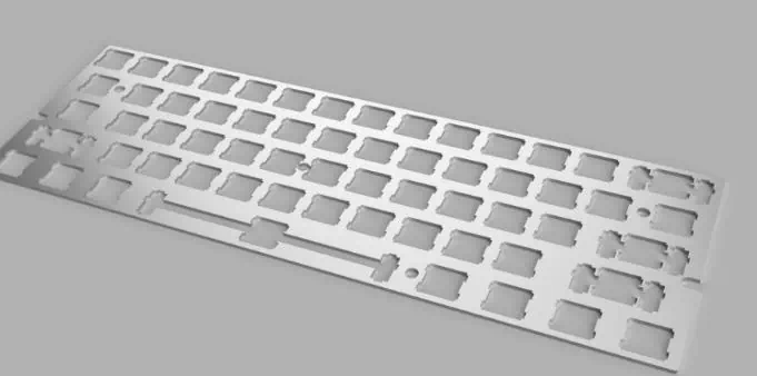
What is Keyboard Plate means? The plate is used over of the PCB for additional help, this keeps the keyboard more steady and from flexing. Commonly this part is not owned in every keyboard. This is the fundamental distinction between the two switch mounted, regardless of they have this plate or not.
Fig. 4 Keyboard Plate Illustration
Diverse Plate Materials. The common materials for plate materials are found in the following list below. There are often new materials being tried as plates, so noted that this is not an fix list. Numerous customized mechanical keyboard, after they are bought, set up the plate documents on the web. This is for individuals who need to print or produce in CNC their plates to utilize on their keyboard. Aluminum and brass are the two most used materials for plates. Other than those two, it is depend on the client to determine materials and constructs their own. Even though there are diverse plate materials, giving them a shot and finding which material which suitable for you is the best method. The various case of materials and switches will also influence the general keyboard’s feel and sound.
Plates from aluminum are the most well-known and used on a custom keyboard. It is broadly accessible and not difficult to cut. Aluminum gives a solid plate that has no bend in the keyboard. This material is a tolerably solid.
Brass is more solidthan aluminum. Gradually, without being dealt with, brass will stain and oxidize after some time. A few people have seen that brass is noisy and bassy. Nevertheless, the other have seen minimum contrast between brass and aluminum.
One of plastic based material used as plate material is Polycarbonate. Nonetheless, it is bassy. Polycarbonate feel bouncy on the PCB and permit bend.
Carbon Fiber. Lightweight and exceptionally additionally tough is carbon fiber characteristics. It permits bendwhen gaming/typing, which gives a bouncy vibe.
In this guide, we have known all differences between PCB-mounted and plate-mounted Switches. The major difference is the pins quantity on the lower part of switches, regardless of whether they are 3-pin or 5-pin. The pins quantity doesn’t have a significant effect, still, the fact that you can basically cut or clip off the additional plastic based pins if your PCB just suitable for the 3-pin mounting. We additionally described the advantages of making a keyboard with a PCB mounting and plate system, for example, contrasts in solidness, feel, and quality. There are a few kind of PCB’s out there that all serve an uncommon features and typing experience, which truly indicate that this is intriguing leisure activity. Following are a few keyboard variations hat you need to know.
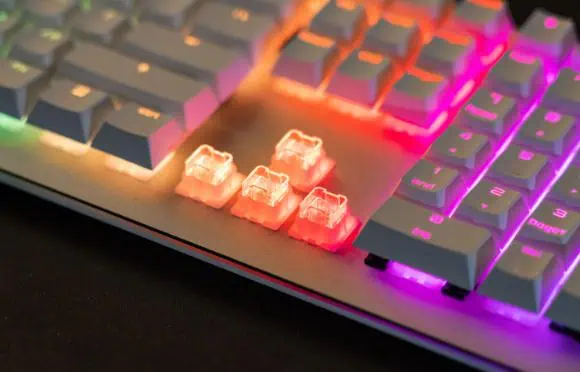
Mechanical Keyboard
Commonly, all modest computer users may assume that all keyboards are equivalent. As they might believe that after all computer users may just type a couple of messages and play out a couple of searching on internet through a day. Nevertheless, choosing a keyboard for the hardcore gamer is on another level, it is very crucial. Having the correct keyboard is about tactual feedback and feel. It is about enhancing gaming experience (and general computing) to the next level. All this about is choosing a keyboard that feels directly in your grasp, which empowers you to reach your best performance. There are two keyboards core types, mechanical keyboards and membrane keyboards. Choosing which type is proper for you rely on a few factors. All things are considered, you may have spent a lot of money and endless hours exploring the best PC parts to purchase. it pays to consider how you will be communicating with your new build as well!
Fig. 5 Illustration of Mechanical Keyboard
The main difference between mechanical and membrane keyboards. The more common keyboards are Membrane keyboards.Thin membrane pushes on a circuit layer, that enrolls the button pressed in membrane keyboards. Compare with a mechanical keyboard, membrane keyboards are less expensive, handy, calm and lighter. Hence, membrane keyboards have weaknesses such are a more limited lifespan, inclination towards a “soft” key feel, just as hard to clean. The last is the incapability to let “key rollover”. Therefore you can just really enlist one keystroke in one time with a membrane keyboard. This implies you shall find the key you push does not enlist. Regardless of whether you are typing or gaming, this can be a big drawback.
Mechanical keyboards are prominent for their particular key-feel. Mechanical keyboards give significant feedback to user. A mechanical keyboard has spring-loaded switches instead of a membrane cap that pushes down on a narrow membrane layer, to a conductive circuit below. These register the key squeezed – frequently with a distinct snap, unique to a mechanical keyboard. An unusual component is their spring-loaded switches – these come in a few distinct feels. The fundamental trinity of switch types are clicky, that give crisp feedback feel; tactile, where a knock in movement gives feedback; or linear, which the keystroke is subtle;. Two or three lesser switch types are quiet, which switch makes insignificant aural feedback, and the speedy, where the key activates as fast as could be expected. Switches can likewise be found in the low profile design that makes key’s travel shorter and thinner keyboard . As of late, there have been a few advances in the key innovation. Razer has made optical switches with low actuation times utilizing a light beam underneath the switch stem. Steelseries’ reaction is their OmniPoint switch that can be arranged to perform at various actuation points.
The other key distinction between the membrane and mechanical keyboards is customization. Mechanical keyboards permit you to alter the keycaps – hence profoundly changing the feel and appearance of your keyboard. On the web, there is no lack of keycaps, which you can modify your keyboard like what you want. If you have an intention to modify keycaps, we display the photographs from our Mechanical Keyboard Mini-meet in display area for your inspiration. Key drawbacks of a mechanical keyboard include sound, weight, and cost. In case you are bothered by the noise, you might need to move from most mechanical switch types and select a silent one. Whereas the various choices of switch design give great feedback, it makes the keyboard’s sound louder than its membrane set, heavier, and costly.
What aspect that we must concern in when purchasing a keyboard. There are a few important points when buying a keyboard. These include the type of utilization, compactness, just as plain personal preference. The sort of Personal Computer activity you might be doing will be consideration to what kind of keyboard you will purchase. In case that you are seldom using PC, moving around a lot, or enjoy playing light games a membrane keyboard might be more appropriate. Are you using PC in almost entire day? Or on the other hand, you are searching for uncommon and special to complete your build with?
Mechanical keyboard will be a good option for you. If you searching for a keyboard that permits you to alter the look at feel of board, or that gives tactile feedback, a mechanical keyboard might be ideal for you. Mechanical keyboard shall raise your gaming experience – improving your build speed in Fortnite, or not any more passed spells in Dota. It additionally consider the keyboard size. If you utilize your PC for a combination of data entry and gaming, a full-size keyboard, with complete Numpad is good option. However, if you utilize your console just to game, a TKL (tenkeyless) design might be more reasonable. Also, if space is at a higher cost than a normal or premium, more compact keyboard, consider smaller one. Membrane keyboards commonly are full-sized, while you can purchase mechanical keyboards in both standard sizes.
Conclusion. A keyboard is associate with PC. However, the two types of keyboards have their favorable pros and cons. At the point when you go to your nearby PC shop, think carefully about the contrasts among mechanical and membrane keyboards. You need to ensure that it appropriately fills your need.
Hot-Swappable Keyboards
Hotswap (can be written hot swap or hot-swa) is an stated attribute that Input Club and Kono Store used early. It depicts keyboards that permit switch substitution without soldering process. Kaihua or Kailh, the first switch producer in China, made the market-overwhelming hot-swap socket design presented below.
Fig. 6 Illustration of hot swappable keyboards
Numerous web site says that hotswap keyboards is built from “hotswap switches,” which is infrequently the case and can create light hesitation. Cherry MX-style switches hotswap keyboards are applicable for keyboards with equivalent hotswap socket plate design/pinout, however they explicitly were not intended for hot swap utilization. Those switches could be soldered / mounted into a standard keyboard. The genuine development lives on the PCB or, if there are real hotswap switches same as our contactless Keystone line / SILO, in the fundamental innovation.
What are the advantages? Hotswap keyboards are quality-oriented manufacturers and liked by typists. They make switch fixes simple (bringing a longer lifetime to keyboard) and take into personalization, yet those are only the base advantages. The simplicity of assembly also makes production in small quantity possibly runs — manufacturers can use extraordinary switches but they can get a lower Minimum Order Quantity, evading huge automation expenditures. On the chance that a keyboard does not own hotswap sockets, its adjustment alternatives are exceptionally limited. In the standard keyboard, you should add Holtites socket and / or solder to alter switches. Holtites sockets are not excessively solid and can just handle with a couple of switch alteration. Those problems vanish with advance hotswap socket designs such as Kaihua’s.
For some reason, Why are not many hotswap keyboards available? The main explanation is profit decrement — both short and long term. Hotswap sockets only change the expenditure a little per keyboard. Most keyboards are inconceivably low cost to make, and created in batches of a few thousand, so companies do not want additional expense which can reduce margin. They additionally make repairs simpler; when switches are broken, people are considerably less likely to purchase another keyboard instead of recover it themselves. Hotswap sockets additionally need some engineering expertise to perform. They occupy an additional space over the PCB so component routing and placement should be exact. This limit worldwide format support on the PCB level, particularly if the keyboard is equipped with LEDs. If you require a split space bar that belongs to a hotswap keyboard or a European enter key, distinct PCB design is generally essential. Keyboards similar to Minivan, which is not, at this point accessible, accomplish incomplete success complete keyboard functionality by decreasing LED functionality.
Conclusion. If you familiar with soldering and have an favorite keyboards switch, hotswap probably won’t be important for you (regardless of whether it offers the quality of lifetime improvement). For people who prefer simple assortment and repairs, nonetheless, hotswap keyboards are great. It is difficult to confirm making something besides hot-swap keyboard as a special keyboard producer; expect to see an increasing number of mechanical keyboards build from hotswap choices available on the market for the following year.
Electronic design. It can be described that mechanical design is another half of electrical design. All the key pushes should some way or another be transferred to the PC. I have never build anything associated with USB or designed electronics system for a keyboard usage before, at the same time, similar to all tasks in this project this appeared to be a great challenge. Each keyboard has its own controller. This processor do several things such as reads the keys, makes an interpretation of read keys to messages that key is pressed, and delivers and deliver messages to the PC. Most of current keyboards use USB connection. The PC only sees a common USB device. This keyboard and some other USB keyboard are just the same. ATMega328P is used as main controller unit for this keyboard. The processor is associated with the key switches and to the PC on the opposite side. Because the controller has no USB port this is copied in firmware with USB. On this prototype, you can see isp header, the processor, I²C connector, 12MHz crystal, programmer, and debug led. There are a few more components on the base.
Fig. 7 The processor using on the prototype board
There are a ton of keys using on a keyboard. Associating all keys straightforwardly to the controller might require a ton of input pins and plenty of wires. Fortunately, there are alternative methods to connect all of those keys. The most widely used technique is multiplexing . All of key switches are connected into a huge network. The controller drives single row at that point and reads all columns for checking whether a switch is pushed on the crisscrossing of that particular column and row. You might find some troubles when more than one key is pressed without a moment’s delay, while this works fine when a key is pressed at one time. The issue is that for a certain mix of keys, sometimes it is read by controller like some different keys are pressed too. People use term ‘ghosting’ for describe this situation. In many keyboards, the row and columns are spreading over the board so that ghosting rarely occurs. A solution to fix this issue could be to add more electronic components. If you add a series diode with each key switch, the ghosting issue might be solved. Sadly the Tipro MID128 keyboard that is used for testing the key format has a ton of noticeable ghosting. Indeed, it shows up so frequently and you can get truly tired of it. Afterward, there is a little improvement that can be done, it must be settled in the design. Due to irritating ghosting issues using the Tipro keyboard, I needed to ensure my design should not have this issue.
There are few alternative approaches to read every single key switch. I decide to utilize I/O expanders for this keyboard. I/O or Input Output expanders have a ton of pins and are associated with the processor through a straightforward 2 wire communication bus. Each expander serves 16 additional pins. So every switch is straightforwardly associated with I/O expanders. General I/O expanders are thusly associated with the processor and this tackled the pin count issue. This methodology is like utilizing shift registers, yet has some more benefits. Microchip MCP23017 is utilized as I/O expanders components, with 16 I/O pins each and internal pull-up. General I/O expanders are associated to the PC via I²C connection. Each I/O expander is configured to a different address and can be called individually.
PCB Design. While you can wired everything inside the keyboard one by one, a more professional and elegant solution is making PCB. This flawlessly interfaces everything and when all the key are assembled, the board likewise adds to the general firmness of the construction. Designing PCB is not excessively different from designing the case. You have to know where all things goes mechanically and afterward make the electrical associations. I used gEDA PCB For this project, one of the GPL’d suit. gEDA PCB is not difficult to use. It probably won’t be as sophisticated as a few of the commercial software, however, it is open-source, and with no limiter. I utilized this software before for a few different tasks (like the tikkenteller, a telephone cost enrollment system) so I use this software again.
Fig. 8 Screenshot of gEDA PCB
Since the keyboard comprises of two parts, we need one circuit boards for each hand. The two parts of the keyboard case are mirror in display, so I contemplated whether it is feasible to make a reverse printed circuit board version, to utilize the same design for the two parts only mirror it. This could not just reduce production expense for PCB (numerous duplicates of a solitary design is normally less expensive than multiple different designs with a single duplicate each), however, be a challenge for design also. The keyboard case is minimized and the greater part of PCB is now filled up with key switches, and it is only limited free space for the other components on the PCB. Utilizing surface mounted components giving an advantage to make wider free space. Shockingly this was used by general I/O expanders. Space for processor is not available. Then the controller unit moved to a different PCB. Since there are 4 wires required between the controller unit board and the half of keyboard (sck, sda, vcc, and gnd) this isn’t a very remarkable issue. Perhaps I will merge the processor in a next version.
All surface mount components require to be at the PCB lower part to be able to genuinely fit the Printed Circuit Board into the case. Top layer PCB is very full. Only the PCB lower part of half keyboard might be the PCB top layer for another half. So I made footprints for all surface mound parts on both lower and upper layer of the PCB. It is enough to make one design for this purpose. There is a slight distinction among upper and lower footprints. Each I/O expander requires to have different I²C address, then the processor can call them separately. The address is configured by giving 3 input pins on general I/O expander either high voltage or low voltage. The top layer I/O expanders are configured to one address, furthermore the ‘base’ I/O expanders are configured to another. Another base/top issue key switches footprint are not asymmetric. The pin on the pin on the left-hand side sits nearer aside and the right-hand side of the switch locates nearer to the top. In result I made a unique twofold sided Cherry MX on the PCB design software. In this form, holes are served for both top and base mount. The other challenge was some of measurement used in PCB are in imperial, however, the rest is metric. For example, the switch dimensions are in inches while the case dimensions and the free space between key switches are in millimeters.
I considered something simpler (and considerably less expensive) than producing and designing a PCB for the processor. I would propose one of the less expensive USBASP boards on eBay. Those are gadgets meant to be utilized as AVR firmware programmers. There is a processor, voltage regulator, crystal, USB interface, headers, led, and a all of various things I prefer to have on the board processor. The USBASP is less expensive on eBay than purchasing parts by parts, not to mention having another PCB made. I’d simply reconnect a few pins and upload my firmware.
PCB Production. After the PCB design was completed, I needed to get the real PCBs. I have home made some PCBs utilizing toner transfer. Print PCB design on a special sheet with laser printer. At that point, utilized clothes iron, transfer toner to PCB material from the paper. In the case of everything works out, you will get the design printed on the PCB raw material. This way worked previously, however this time was different. I made a few endeavors with various printers, various kinds of paper, and various types of PCB, yet nothing get done. At last, I surrendered and, produced it in online vendor.
There are numerous places to print and make PCBs. Some are high grade, some are quick, some are less cost, some are not. When you produce it in China you can save money on production costs, yet it may probably won’t be the best grade and longer time to finish. Saving expenses would be good, however more necessary for me is that PCB or other components is delivered with honor for the environment and the worker. Chinese PCB manufacturers prefer reducing expenses by giving low payment to their workers and unloading synthetic waste in the environment. I would preferably spend more on a PCB over permitting this to proceed. With a several comparison and looking I settled on Jackaltac. Their PCBs are made in the UK.
Brand like Razer, HyperX, Corsair, and so on, take the greater part of the spotlight in mechanical keyboard market. Most of these brands guarantee to offer the best functionality and quality, however, that is not generally the case. While the famous gaming brands have driven the reception and awareness of mechanical keyboards become the standard, make a deal on quality are quite often made to bring down costs. At the point when you look at your choices, the difference which will you find is only on the outward design. Pick your switch, pick your design—that is all.
Fig. 9 Illustration of mechanical keyboard
Yet, imagine a scenario in which I revealed to you that all aspects on the a keyboard can be arranged and customized. This goes a long way beyond only purchasing the most recent keyset from Massdrop or trading in an weaved connection. With pre-assembled boards, you do not get to pick the layout or size. When you need a programmable keyboard with 60 percent layout and having devoted arrow keys yet it is just accessible without the programmability, at that point you should make a deal and pick the features that are generally imperative to you. In case you do not want to compromise it, it will be good to assemble your own keyboard.
If you are wanting to do any DIY project, it is important for you to understand which components you have to purchase. The exact thing you need is working with soldering tool just to know you are missing a principal parts. There are six parts you will have to assemble to make a keyboard alongside a USB link: Enclosure, Keycaps , Key Switches, Mounting Plate, PCB, Stabilizers,.
All of parts have a wide scope of alternatives to customize your keyboard and numerous choices for one part can affect or restrict your choices for another. Picking the correct shop to purchase your parts can be quite troublesome if you’ve never make a keyboard. Your first sense may be to jump onto Amazon and begin looking for parts. You can figure out some great choices however it’s a lot simpler if you can get different parts from a same shop.
There are a some of various stores I often purchase my components. KBDfans has an enormous parts and they convey a larger number of PCBs and enclosures than any shop that I know. It’s completely feasible to get all components you require from them, yet their keycap selection comes up short. The other one-stop shopping place for mechanical keyboards components is 1UP Keyboards. Their case is not as strong as KBDfans yet if you are in US, you may reduce cost on shipping by buying from them. In case you’re searching for standard keysets, both of these stores will be enough.
Assuming, as if you are searching for something more extraordinary and with a more extensive compatibility, you will have to find it in the other supplier. Massdrop is an incredible place to get more costly and limited keysets at notable savings in case you are patient enough to sit tight for drop and ship process. In case you do not want to wait and ready to pay more, Originative gives various keysets from high-grade brands like Signature Plastics and GMK. Presently, before you spend money on everything without exception, we will talk more deep for each part so you can understand how they work together.
When you have arranged a workspace far from flammable items, you can begin assembling everything. The essential process resembles this:
There are not many improvement you can perform to make it simpler. The absolute thing is to guarantee you follow work step by step. Your stabilizers can not be mounted over on the upper plate section and your switches can not be mounted under it, except if you ought to do extra work with solder sucker.
Stabilizers Installation. Stabilizers installation is quite easy. Adjust the prongs to the proper holes in the Printed Circuit Board and push them in. The direction, though, is important.
Fig. 10 Installing stabilizer on keyboard PCB
The plain with the stabilizers need go assemble in the bigger PCB holes meanwhile the ends with clips must be mounted on the smaller holes. When you mount them in different way, they won’t remain in. The first thing you need to do is getting it to the huge holes and afterward push the opposite and mounting the stabilizers to the smaller holes. You may need to apply right pressure to make the clips to near one to another. It ought to be noticed that stabilizers are not cover with grease from the producer before start soldering it. This implies they can be somewhat noisy, yet can be eased by applying a little grease to the connection points. WASD sells silicone-based grease for two or three dollars.
Adjust and Solder. It is difficult to keep the keyboard plate lined up with the PCB if you are attempting to put all switches in one time. For an ideal arrangement and to maintain the plate level, at first mount and solder the 4 corner switches. You can assemble the base row and test keycaps. The base row normally has numerous switch placement choices to oblige unique space bar and modification. It will be good to check the fitment and solder one switch than to desolder a whole row.
Fig. 11 Align and solder keyboard PCB
Before soldering components, ensure your soldering iron temperature is enough, and remember to clean the tip. Applying a little solder to the tip raises conductivity and soldering become quicker which will secure your board. Each solder joint might require close to two or three seconds. Try not to keep the tip squeezed the pad for more than that. it can make the pad broken and lift from the board. Clean the tip with a sponge and afterward tin on the clean surface.
Right, when you are tinning, it is the exact time you ought to be touching the solder tip (on soldering iron) to the solder. For a solid solder joint, heat the switch terminal and pad while provide tin to solder from the other side. Your solder have a synthetic cleaning chemical named flux which can’t tackle its work if it never contacts with the soldering surface. A decent solder joint will have a pleasant shine and not bubble.
Last Assembly and Keycap Mounting. The last assembly process ought to be very simple if you have used a screwdriver previously. Ideally, you have left the small screws for securing the PCB to somewhere protected as yet—they simply get lost .
Place the assembled board to the enclosure and keep the screws save. Commonly, it may have 5 mounting points yet your PCB may have four. This is okay, four screws will be enough to hold the entire board. The final activity is installing or mounting your keycaps. Press each keycap to the stems of all switches and you’re finished. If you follow this guide, you willl get extraordinary, just for you, to your specifications and appetite.
Printed circuit boards (PCBs) have become exponentially more sophisticated over the past decades, transforming from simple single-sided boards to complex multilayer designs pushing the boundaries of materials science and fabrication technologies. This evolution enables PCBs to serve at the heart of today’s electronics innovations from commercial wireless devices to mission-critical aerospace systems. To turn cutting-edge PCB designs into physical reality requires robust, advanced manufacturing capabilities spanning automation, precision processes, testing, and quality control. This article will examine the most advanced PCB manufacturing capabilities defining the current state-of-the-art.
High Density Interconnect (HDI) PCBs
HDI Board Lamination Times
High density interconnect (HDI) PCBs integrate incredibly fine lines and spaces, microvias, and other attributes enabling dense component mounting and multilayer stacking.
HDI provides the layering that allows complex ICs to interconnect in tiny PCB footprints. The advanced processes, materials, and precision required pushes manufacturing state-of-the-art.
Embedding passive components like resistors and capacitors along with active ICs into the PCB layers conserves space while enhancing electrical performance.
Additive methods like inkjet printing are beginning to complement or replace conventional subtractive PCB processing.
Key Additive Process Capabilities:
Inkjet solder mask, legend, and markings deposition
Print-n-peel temporary masks for etching
Direct copper printing on substrates
Printed dielectric and conductive adhesives
Rapid prototyping of traces
High mix/low volume customization
Reduced chemical waste versus subtractive
Finer resolution than standard methods
Additive techniques enable new environmentally friendly fabrication work flows.
Conclusion
This overview of advanced PCB manufacturing capabilities illustrates the tremendous innovations propelling the industry forward. From exponential densification to embedding actives inside the layers, fabricating the PCBs that underpin emerging technologies involves immense expertise and process mastery. Through continual development of these sophisticated manufacturing capabilities, PCB fabricators enable designers to turn visions of cutting-edge electronic devices into reality. The future will certainly bring a new realm of techniques allowing PCBs to progress supporting society’s growing technological demands.
Frequently Asked Questions
Q: What are some emerging HDI technologies on the horizon?
HDI continues advancing with thinner dielectrics, smaller microvias, printed embedded passives, sequential laminations, increased layer counts, and improved modeling – enabling further component densification. Laser direct imaging down to 5um lines will enable finer densities.
Q: What limits manufacturing capabilities for higher frequency PCBs?
At high frequencies, inconsistencies in dielectric thickness, copper surface roughness, resin purity, glass weave, lamination pressure, and other variables degrade performance. Each process must be tightly controlled to avoid signal losses.
Q: What are some challenges when embedding actives in PCBs?
Embedding actives introduces fabrication intricacy in cavity formation, dielectric material selection, thermal dissipation, electrical interconnect, reworkability, signal isolation and simulation. As more actives are embedded, the manufacturing expertise required also increases.
Q: How are very small microvias formed?
Laser drilling is required for microvias under 8 mils diameter. Laser produces clean, precise holes versus mechanical drilling even through complex layer stacks. Tight process controls are needed for capturing via depths accurately.
Q: What are key differences when manufacturing large format PCBs?
Challenges arise in handling large, thin panels across processes. Alignment and registration becomes exponentially more difficult at large sizes. Thermal stress and warp control is crucial. Conveyor widths, tank sizes, lamination presses and other equipment must be scaled up.
Determining the right printed circuit board (PCB) thickness is an important aspect of the design process. The thickness impacts manufacturing feasibility, component clearances, stiffness, thermal performance, weight, and cost. With PCBs becoming more complex including embedding actives and passives, the number of layers increasing, and higher density designs with HDI, selecting appropriate board thicknesses is more nuanced than ever. This article will provide guidance on how to optimally design PCB thickness to meet mechanical, electrical, and fabrication requirements.
Key Factors In PCB Thickness Selection
Several interrelated considerations influence the choice of PCB thickness:
Number of layers – More layers require greater thickness to accommodate inner layer spacing. High layer counts (>36) drive thicker designs.
Component height – Clearance must be allowed between tallest components and outer layers for assembly and preventing shorts.
Routing density – Compact routing of fine features needs thicker cores for trace impedances and layer separation.
Stiffness – Thicker boards provide more rigidity, important for large PCBs and minimizing flex stress.
Flex portion minimum bend radius: 10X board thickness If 0.1” bend radius needed → 0.1/10 = 0.01” minimum thickness
Total Minimum Thickness
Copper: 3.45 mils Dielectric: 15 mils Clearance: 150 mils Bend (N/A here): 1 mil
Total: 168.45 mils (0.168”)
Round up: 0.170” minimum thickness
This methodology can be followed to calculate minimum workable thickness for any PCB stackup and design constraints.
Adjusting Thickness for Functionality
Beyond the bare minimums, PCB thickness is often increased to optimize performance or fabrication. Common reasons include:
Trace Impedance Control – Matching trace impedances requires specific dielectric spacing. Thicker material may be needed between layers to achieve target impedance.
Signal Integrity – Thicker dielectrics reduce capacitive coupling and crosstalk between layers.
Noise Isolation – Additional dielectric layers helps isolate sensitive analog signals from noisy digital routing.
Rigidity – For large boards (>15” edge), increasing thickness adds stiffness to counter flexing forces.
Warpage Reduction – Symmetric center-core construction with thicker dielectrics minimizes warpage from manufacturing stresses.
ESD Resistance – More dielectric buildup helps withstand electrostatic discharges in high voltage applications.
Thermal Management – Added inner layers enables lateral heat spreading while minimizing impact on thickness.
Embedded Components – Cavities for embedded actives and passives require extra thickness.
In each case, the cross-functional design team weighs the tradeoffs of increased thickness against other constraints to find the sweet spot.
Standard Thickness Increments
Rather than arbitrary values, there are common PCB thicknesses used across the industry:
PCB Thickness
Number of Layers
0.031”
2
0.062”
4
0.093”
6
0.125”
8
0.156”
10
0.187”
12
0.218”
14
0.250”
16
These standard thicknesses align with typical layer counts and offer sufficient margins for most applications. They provide a good starting point when estimating initial thickness. As the design progresses, the thickness can be dialed in based on specific requirements.
Of course, specialized or high complexity designs may warrant going outside these general ranges. But they provide a reasonable starting point when estimating thickness by application.
PCB Stackup Configurations
There are several stackup arrangements that impact overall thickness:
Symmetric
Layers are distributed equally about the center core. This avoids mechanical stresses from asymmetric construction. Often used for >8 layer designs.
Asymmetric
Layers are grouped toward one side of the center core. Can cause bowing but uses less dielectric. Often used for simpler <8 layer boards.
Core Thickness
Alternative core thicknesses like 0.024”, 0.049”, or 0.081” can be specified when total thickness requirements differ from standard sizes.
Buried Cores
A buried core adds rigidity for ultra-thin boards. A thin core is laminated between outer buildup layers. Allows high layer count in minimal thickness.
Mixed Cores
Different core thicknesses can be combined for complex requirements. Thinner base cores reduce weight while thicker inserted cores add rigidity.
Copper Balancing
Equal thickness copper layers on extremes minimizes curl and wrinkling. Heavier internal planes provide planarity.
The right stacking arrangement contributes to optimizing the finished board thickness.
Panel Thickness vs Final Thickness
Thickness Ranges
It helps to distinguish between:
Panel thickness – The initial PCB panel thickness through fabrication, often slightly thicker than final thickness.
Final thickness – The completed board thickness after processing. May involve post-fabrication steps like surface grinding to achieve final thickness target.
For example, a 0.100” final thickness board may use a 0.104” or thicker panel to allow for processing variances and finishing.
Thickness Tolerances
Standard PCB thickness tolerance is ±10% of the nominal value. However, tolerance can be reduced to ±5% or tighter when holding tight finished thickness is required.
Tighter tolerances often warrant steps like starting with oversized panels and grinding down precisely to achieve specified thickness.
Markings For Thin Boards
For rigid boards under 0.031” thick, fabrication notes indicating “Thin Board” alerts manufacturing processes must delicately handle the thinner material to avoid damage.
Flex Circuits
Flex PCBs involve separate considerations for minimum bend radius, flex layer thickness, stiffener thickness, and other unique constraints.
Consult the Fabricator
To ensure manufacturability and avoid surprises, always review your thickness design requirements with your PCB fabricator early in the design process. An experienced manufacturer can validate your design or suggest improvements.
Conclusion
Designing the optimal PCB thickness requires juggling mechanical, electrical, thermal, fabrication, and cost considerations. Following the guidance in this article will help you select appropriate thicknesses to meet your product needs while enabling efficient manufacturing. Partnering closely with your fabricator is key to optimizing thickness. PCB thickness may seem like a simple issue, but deserves thoughtful design consideration given how foundational it is in determining the quality, cost and performance of the end product.
Frequently Asked Questions
Q: At what point should PCB thickness be considered in the design process?
A: PCB thickness parameters should be estimated starting in the preliminary design stage based on likely layer count, component height, compliance requirements, etc. As the design progresses, thickness can be refined after spacing, stackup, embedded components, and other details are worked out. Consult the fabricator early to validate thickness feasibility.
Q: How does thickness impact the cost of PCB fabrication?
A: Generally, thicker PCBs cost more to fabricate than thinner ones due to increased materials usage. However, ultra-thin boards under 0.020” can also cost more due to additional handling care required. Moderate thicknesses between 0.062” – 0.125” are often the most cost effective.
Q: Can PCB thickness be increased by adding copper rather than dielectric?
A: Yes, thick copper up to 20 mils can be plated onto layers to add rigidity and thickness without impacting dielectric spacing. However, thermal performance diminishes as the board heats up faster due to higher copper content.
Q: What are recommended clearances between components and outer board surfaces?
A: For circuit boards under 24V, a minimum clearance of 0.015” (15 mils) between components and outer surfaces is typical. For higher voltages, greater clearances are advisable, sometimes up to 0.250” (250 mils) or more.
Q: How are very thick PCBs above 0.250” fabricated?
A: Extremely thick boards can be manufactured by laminating separate 0.250” cores together. The individual cores are bonded under high pressure and temperature to form a single thick board ready for further processing. But such thick boards can be challenging to fabricate and often unnecessary.