What are the Design Considerations for Tab Routing?

PCB Routing

Tab Routing (Tab Route PCB) because automated equipment for circuit board assembly frequently struggles to work with the smaller boards, assembly errors occur more frequently.

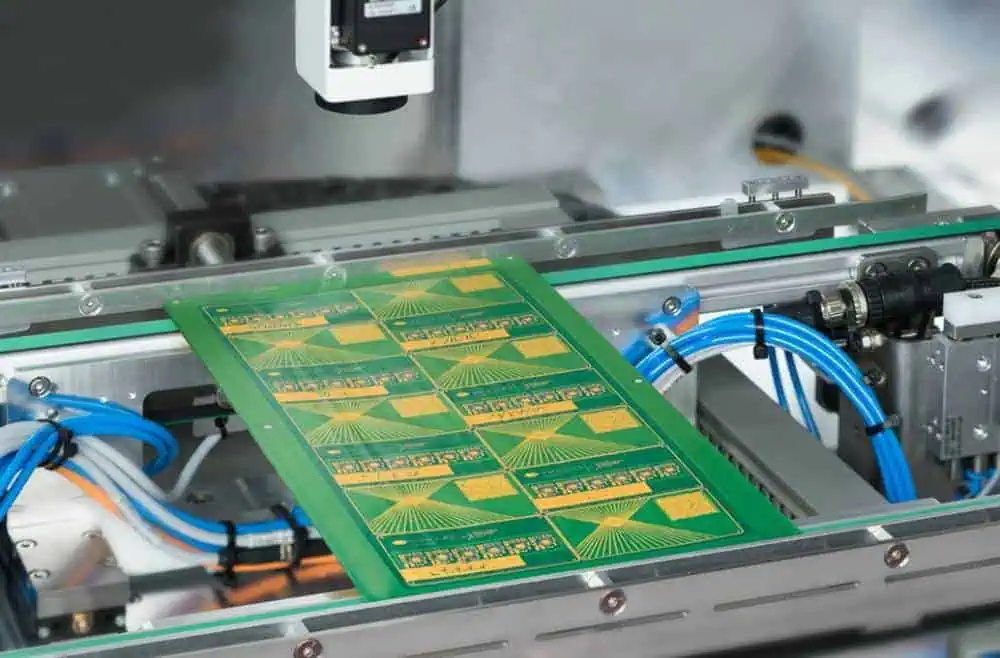
Several businesses employ a technique called panelization, which produces a Circuit board panel, to reduce these flaws and increase manufacturing process efficiency.

YouTube video

What Does Tab Routing Mean?

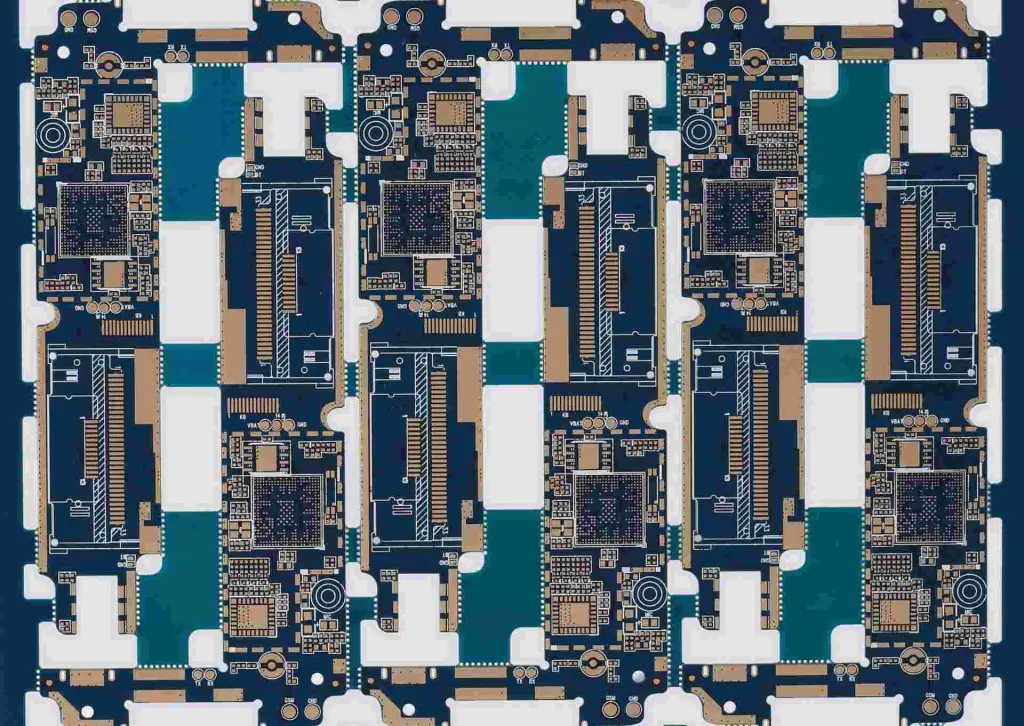
PCB panelization can also be known as tab route, as well as tab routing, and it involves arranging many boards of the same and various designs into a panel. This common technique for PCB panelizing makes use of tabs without or with holes.

During the tab route PCB construction process for panelized boards, single boards can be detached by severing or cutting those tabs which are located between the boards or between its array rails and boards.

Several circuit boards can be fabricated and assembled in one go using a panelized Circuit board array with tab-routing. As a consequence, the project’s expenses are reduced, and the Circuit board order is completed more quickly. Choose the perforated kind if you want to manually separate the panelized Boards. Use a specific depaneling tool, such as depaneling carriers to avoid board damage when you believe that removing the PCB from this assembly array will put an undue amount of stress on a tab route PCB.

The ability to create non-rectangular boards is one benefit. Tab-routing, on the other hand, has the drawback of using more board material that might raise your prices. The board around the tab may also be put under extra strain as a result. Avoid putting PCB components extremely close to the tabs to reduce board tensions. Although there isn’t a set distance for positioning parts close to tabs, speaking generally, 100 mils seems to be the recommended distance. With larger or thicker Circuit boards, you might also need to space components apart by upwards of 100 mils.

Circuit boards in panels could be taken out either after or before assembly. The most popular method is to disconnect the PCBs once the panel gets put together since the PCB panels usually make assembly simpler.

Tab Routing Design Considerations

laser-cut-pcb

In situations whereby components are situated extremely close to as well as over the edge, tab routing is typically recommended. It is also preferred for PCBs with non-rectangular geometry, such as circles. To guarantee the strength as well as operation of such arrays, particularly during this breakout process, numerous design decisions must be taken since the tabs serve as the arrays’ breaking points. These factors include, among others:

Clearance

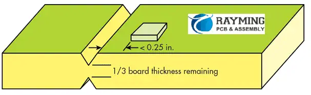
Keep traces and parts at minimum 1/8 inches from the tabs due to the tension put on its breakaway points as well as the risk for splintering.

To guarantee minimum interference, the surface-mounted ceramic multilayer chip capacitors should be maintained farther away, a minimum of 14 inches from its tabs.

Knock-Outs

To avoid problems during the wave-soldering process, the placeholder, also known as a knockout, could be necessary if the PCB design has holes that exceed 0.6 inches. Knockouts are especially crucial in the centre of the array, when PCB arrays become more inclined to droop. While bigger, more atypically shaped knockouts might need numerous three-hole tabs that are perforated, rectangular and smaller knockouts may include a broad, perforated tab (5 hole) on one edge.

Tab Positioning

Maintaining the PCB array design’s integrity is crucial. Perforated tabs (Five-hole) must be spaced per 2-3 inches across the edge of a board, as well as perforated tabs (three-hole) must be spaced each 1.5 inches. To prevent a board’s edge from curving, tabs must be positioned as near to it as feasible. Nevertheless, tabs shouldn’t be put under any overhanging components. Your designer should also make sure these tabs are adequate for supporting the boards without obstructing the breakout procedure.

Placement of Perforations

If you wish to prevent protrusions from your board’s sides, never run tab perforations along a tab’s center; rather, run them near the PCB’s edge, or on every side of that tab if positioned between two printed circuit boards.

Array Arrangement

To ensure uniform break-lines across the array, place PCBs such that all tabs that are broken at once are collinear. If break-lines here are not consistent, certain tabs could break whereas others are merely pushed perpendicular to such board surface that will damage the lamination.

Your design must meet few problems throughout the manufacturing as well as breakout processes if these factors are taken into account.

V-Score vs. Tab Routing

FULL PCB MANUFACTURING Quote

Whatever PCB design you’re dealing with will play a significant role in your decision to employ tab routing or v-score methods in the PCB panel. Before deciding, take these things into account:

Board Shapes: The panelization process heavily depends on the PCB’s shapes that make up an array. For rectangles or square board types, the V-scoring will work well.

When dealing with odd forms, tab routing seems to be more suited.

Edge Components: Tab-routing or a version of it may be preferable to V-scoring if your PCB needs the availability of the edge-hanging components as well as components positioned close to the edge. Just make sure the tabs aren’t close to such edge components.

Edge Quality: Tab-routing might well be preferred than V-scoring if the edge quality is a consideration. Despite the fact that the method leaves behind a few tiny, rough laminate nubs, these may be readily removed with sandpaper, and the rest edges remain smooth due to the routing. On the contrary side, V-scoring produces rough edges around, which might also need additional sanding if clean edges are required.

Time Expense: Since tab routing needs a great deal of time upon that router, it often requires more effort and time to set up. On the contrary, V-scoring, takes substantially less time on the computers.

Waste: V-scoring provides the most advantage when material waste seems to be an issue. The process wastes a lot less material compared to tab-routing, which results in a lower cost for every board overall.

Defaults for Tab Routing

If there are no panelization remarks from customers, our CAM experts will put up the panelized tab-routed array using the specifications shown below. Verify the specifics of our journey and keep panelization.

  • Position the tabs so that they are at a minimum of 9 mm from each board corner.
  • Place tabs on center or at minimum 9mm away from datum holes.
  • Use the 2mm router. Boards must be spaced apart by at least 2mm.
  • Where feasible, make sure these tabs are positioned in one straight line having an X-Y axis.
  • Don’t tab the traces or part holes that are close to the edge of the board. This is to prevent breaking traces or holes.
  • The tab’s width is between 3mm +/- 0.25mm.
  • The tab position tolerance has a dimension of +/-0.5mm.
  • On the 0.5mm grid, tabs must be dimensioned into the center.
  • Place tabs on the outer edge of the board at minimum +/-6mm from every radius.

PCB Panelization Benefits

PCB panelization has advantages beyond only making smaller circuit boards fit into common production procedures; it also improves production efficiency. Additional benefits of Circuit board panelization are discussed below:

The ideal method for producing circuit boards in large quantities is PCB panelization, which saves time and money.

Handling a huge sheet as a collection of smaller boards is a quicker and more effective approach. The cost-effectiveness of employing the standard size of the fabricator for the boards allows for the fabrication of more boards in a shorter amount of time.

Furthermore, PCB panelization gives designers a way to incorporate distinctive designs in prototypes that are more affordable and effective.

Circuit boards are shielded from shocks as well as vibrations. These come from the occasionally harsh environment of a production line via PCB panelization. Hence, via manufacture, it ensures the security of the boards.

PCB Boards Breakout Instructions

Even with excellent PCB array design, issues can still arise when handling the breakout. A board can be completely destroyed by the breakout if done incorrectly, resulting in component damage, splintering, and ripping. Because of this, using effective board breakout techniques is crucial to minimizing expenses. To prevent any such problems, keep these rules in mind as you work through the process of breakout:

Hand Tab Breaking: With the right hand tools, a correctly constructed tab routed Circuit board panel is frequently breakable. Employ wide-nose pliers for bending every tab inside a break-line. This is done till it loudly fractures for the greatest results when using hand tools. Bend these tabs into the other direction so that they fully split along its break-line.

Breaking Tabs with Machine: The board might occasionally become too thick enough to completely break by hand. It could be preferable in this situation to use a cutting instrument. As was the case with solid tab type of panelization, a depaneling router could be a wise choice.

Cutting V-Grooves: A certain kind of a depaneling machine is needed to release panels with V-Scores. This machine employs a pizza-cutter-style blade, which is reasonably priced and needs no upkeep. The edges are going to be somewhat harsher than choices with routes, but that is the only downside.

Conclusion

In situations whereby components are situated extremely close to as well as over the edge, tab routing is typically recommended. It is also preferred for PCBs with non-rectangular geometry, such as circles.

A Comprehensive Guide on the Aircraft Wire Harness Assembly

Wire Harness Manufacturers

In order to carry current as well as electronic signals out of the nose to the tail, the aircraft wire harness assembly plays a crucial role as the aircraft’s nervous system. From the fuselage harness to the power distribution assembly, wire harness makers create extremely intricate electrical harnesses as well as harness assemblies enabling the operating as well as controlling of practically every component of the aircraft. Such assemblies are frequently used in applications which require intricate electronics and dense wiring.

High-performance cables and wiring that are flame-resistant or resistant to the majority of fuels, solvents, or lubricants are used in the construction of the aircraft wire harness assembly. Cobra helicopters, trainers, fighter jets, and other aircrafts, use aircraft wire harness assemblies because they are built to deliver dependable, high performance even under the most challenging environmental conditions.

YouTube video

What is Aircraft Wiring Harness?

wire-harness-manufacturers

The most typical part of aircraft engines is the wire harness. It is a collection of electrical cables enclosed in an insulating substance. This insulated substance is primarily thermoplastic, that is noted because of its versatility. This thermoplastic offers electrical insulation towards the application while being able to handle hard conditions and high temperatures.

It is crucial that such materials utilized to house these wires be robust and capable of withstanding the movement as well as vibrations of aerospace applications in conditions where tear and wear are particularly likely. Such harnesses are sometimes mistaken with the cable harnesses, however they are two different parts.

Why Is the Wire Harness Crucial for the Aerospace Industry?

Wire harnesses can be customized for a particular application. It is essential to utilize components which can survive harsh environments in aircraft applications. Because of their extraordinary flexibility, wires are perfect for confined, compact places. For some purposes, they are preferred over wires.

Also, because they are significantly lighter than cable, the wire harnesses seem to be preferable. Weight plays a significant role in the process of manufacturing for aerospace applications since the aircraft must be able to securely transport big loads of passengers or cargo for, in certain cases, extended periods.

Manufacturing of Electrical Cables and Wiring Harnesses for Aircraft

Conductor wires enclosed in insulated covers make up the wiring harness. Such jacketed cables could be singles, triplets, twisted pairs, etc.

Copper and Aluminum are the two conductors that are most frequently utilized, with each having unique properties. There is a lot of use for aluminum because of its light weight, which allows for long spans as well as its comparatively large diameter meant for a specific conductivity, which lessens the release of electricity out from wires. Copper is easier to solder, has a better conductivity, and a comparatively high tensile strength.

Inside the aerospace sector, an aircraft’s wiring harnesses might extend for miles. Uses include those for the wing, engine, fuselage, and landing gear.

Advancement of the Aircraft Wire Harness Assembly

Advances in Aircraft Technology

In the high-tech world of today, flying could appear like a routine activity that the majority of us have already done. Nonetheless, because of its lengthy history, aviation technology has advanced significantly. Aerodynamics has been the secret to traveling from one location to another when airplanes initially flew. The earliest aircraft to transport people were thermal airships, sometimes known as hot air balloons.

But, developments in aerodynamics as well as motor technology throughout the beginning of the twentieth century increased the prevalence of powered-controlled flights. These early versions, which resemble modern aircraft, were created by 1909. Since aircraft engines have become more powerful and aircraft wiring harnesses have undergone new developments, aerospace engineering has progressed over time.

Without technological advancements, aircraft as well as the aviation industry would not operate as it does today without the breakthroughs experienced technologically.

Nonetheless, despite the advancements it has introduced to the aerospace sector, an aviation wire harness performs the same basic purpose like other wiring systems.

Why Do Wiring Harnesses Exist in Aircraft?

FULL PCB MANUFACTURING Quote

Early on in the creation of airplanes, there wasn’t anything like wiring harness because there were no electrical systems. They were limited to utilize structural components, ropes, including pulleys for moving its flying control surfaces.

Soon, these metal cables took the place of such ropes; today, numerous planes still use pulleys and cables rather to “fly by wire.” A battery, switch, as well as light bulb were eventually added by an aviation designer after he finally chose to wire inside a light. By using cables to connect these components, he built the first-ever electrical lighting systems for the airplane.

As this system simply needed a few wires, its harness manufacturers placed each one in a secure area.

Other architects then followed suit and added additional electrical infrastructures. Although groups of wiring flowed from one section to another, the aircraft mechanics ultimately recognized they have been installing the cables one after the other. Moreover, they required additional wires for every such device.

The setup procedure took a long time. To boost productivity, mechanics started bundling cables together as well as routing them. The aviation sector took notice & thought this was an important development. They connected the wire bundles there after conceiving them as one unit. They did this to produce the first-ever wire harness. These wire harnesses for aircrafts serve this function.

The Functions of the Aircraft Wiring Harness Assembly

The wire harness of an airplane controls electrical impulses for the entire aircraft, just like the harness of a car does. Among the things it controls are the landing gear, engine, wings, as well as fuselage. There is frequently a lot going on within the wire harnesses. An aviation wiring harness is made up of miles of wires, cables, as well as tens of thousands of components. Also, they must all work together to maintain the plane’s smooth flight.

The quickly evolving technology and updated aircraft electrical connections that may accommodate cutting-edge upgrades must also be kept up with by today’s aircraft makers. An aviation wire harness not only increases manufacturing and production efficiency but also makes it simpler for mechanics in repairing and identifying plans that are experiencing some technical difficulties.

The requirement to install a massive plane’s electronic equipment separately is removed by wire harnesses. The afflicted component must be identified by mechanics in order to be repaired when issues emerge and maintenance is necessary.

Aircraft Wiring Harness Assembly Components

When building a plane which complies with military requirements, there are several factors you’ll need to consider, including the aircraft that it will be utilized in. This will influence the precise features as well as the wiring harness components. These include the three different categories of airplane parts.

Standard Components

The military frequently has the ultimate say about MIL-SPEC components in the electrical system of a plane. Nevertheless, before you think of certain firms as approved suppliers, the government should certify them.

Non-Standard Components

Variants of commercially accessible components that adhere to a marginally different military standards commonly make up non-standard components. Original equipment producers may set their own standards for the non-standard components.

Original Equipment Manufacturers can also choose which of their suppliers they want to allow to manufacture the non-standard components. The non-standard component for an aviation harness, however, usually costs more because there aren’t many of them.

Commercially available and off the shell components

Manufacturers develop off-the-shell components in large quantities in accordance with customer demand and market research. Without the approval of the government and the military, the manufacturer can improve its component designs. Any manufacturer can make their own parts and give each one a special part number.

Similar to the remaining two components, these alternatives are available from manufacturers for a lower price. Yet, manufacturers have sole control about how the components are distributed, giving them the ability to set the prices as well as decide on the market share. Also, they are free to change or adjust any requirements.

However, it can become problematic if new wiring harness components are required because the supply is running low.

Aircraft Connection and Wiring

Aircraft PCB

Wiring in the aircraft wire harnesses can be miles long. As a result, careful planning and structuring are required to avoid issues after as well as during construction. Creating a schematic within the CAD software seems to be the initial stage in the design process. This acts as a blueprint for further construction.

There was once a single type of insulating material that could be utilized to fulfill all needs, however today there are many possibilities. Which cables are used depends on the signal that you send as well as the electricity of the system. With these factors, wire insulation will also shift.

It would also be beneficial to label the wires enough so assembly as well as repairs don’t confuse them. However, keep such three things in mind when choosing a connector. The connector’s maximum connections must come first. ach wire’s thickness comes in second, followed by the kind of wire that goes into the aircraft connectors.

Aircraft Wire Harness Assembly Wire Selection

A system level is the place to start when designing the electrical system of an aircraft. The system diagram displays the bigger parts and their connections. The specification as well as size of these wire are not specified; they are merely joined together using a line in the system schematic.

Moreover, the wire splits are absent from this system schematic, such as whenever it goes through the bulkhead using two connectors. Despite its simple construction, the schematic would specify the kinds of signals which the wire would carry. The graphic also indicates the locations where shielded cables, twisted pairs, quads, and triplets are required.

The kind of signal the wire will broadcast as well as the current carried should guide your choice of wire. Usually speaking, you should choose the wire with its smallest gauge which has the ability to carry the needed current.

Also, reliable CAD software would figure out each gauge size’s current-carrying capacity automatically.

Testing of aircraft wire harness

Wiring analyzers are automated pieces of equipment used to assess aircraft wire harnesses. Wiring analyzers are made by many companies. Special programs instruct the analyzer on the tests to be performed, the voltage and current to be used, and the duration of applying current. Utilizing adapter cables, the technician joins this wiring analyzer onto that wire harness.

Insulation resistance and continuity are the two most often used tests. However, wiring analyzers are also capable of doing other tests, such as checking the functionality of diodes and conducting tests on the AC dielectric and empty contact cavities. They can also turn on lights and relays and measure capacitance and resistance.

Testing for continuity makes ensuring that every wire gets connected in line with the specific design. Continuous testing are run at 0.5 amps with constant voltage as well as a 0.2 second minimal dwell time.

The megohm test, commonly known as an insulation resistance test, looks for any short circuit. For instance, this insulation resistance testing will reveal a short circuit if there are two wires adjacent each other and both have nicks present in the insulation. This test on insulation resistance will also reveal a short circuit when a connector is improperly made and there isn’t sufficient material to divide two contacts.

Tests on insulation resistance are conducted with a continuous current at a value of 1,500 VDC and a 0.15 second minimum dwell period.

The test on insulation resistance performs exactly what its name implies: it guarantees there was enough resistance in-between 2 as well as more conductors to prevent short circuits. If this resistance is larger than one hundred megohms, then the test is passed.

Most OEMs prescribe how wire harnesses should be tested. MIL-STD-202 is the most popular military test specification.

Conclusion

Aircraft wire harness comprises several cables and connectors. Furthermore, other standard, non-standard, as well as commercial-off-the-shelf (COTS) parts complete and function the harness. You must consider your requirements before selecting the elements. The schematic will then be designed utilizing CAD software.

What are the Types and Applications of High Tech PCB?

SSD PCB

Printed circuit boards are core components of all electronic devices. They serve an important role in revealing the functioning and performance of an electronic device. On these boards are electronic components mounted on. These boards create electrical connections between components and offer mechanical support. PCBs are usually fabricated to meet the requirements of the applications for which they would be used.

Some particular kinds of printed circuit boards can be more complex and challenging to fabricate compared to others. These kinds of PCBs would need more steps in their manufacturing process. A good example of such boards is high tech PCB. High technology PCBs are more complex to fabricate. This is because these boards can feature high layer counts, can be made out of exotic materials, and may need additional fabrication and design processes with tighter tolerances.

What is a High Tech PCB?

Rogers RO4533

A high tech PCB is a type of circuit board that requires complex fabrication process. A circuit board is classified as a high tech PCB based on some factors. These could be the number of layers, the material used in fabricating them, the feature they offer, the technology used in fabricating these boards, and more.

There are good examples of a high tech PCB. Examples include ceramic PCB, multilayer PCB, High density interconnect PCB, flexible PCB, and rigid-flex PCB. A high tech PCB requires technical experts to manufacture since there are fabrication processes require strict attention. Also, it is important to note that this kind of PCB is usually fabricated with high demands.

It is only possible to fabricate a high technology printed circuit board if it is made of industry standard materials. Furthermore, the design and fabrication processes are usually well-defined. It is important to check every process is for the expiry of the treatment period.

It is ideal to check the quality of the material, mechanical features, and the shape of the holes of a high tech PCB. The design and manufacturing process of a high tech PCB is very complex and as such PCB manufacturers need to pay attention to these boards.

Characteristics of High Tech PCB

A high tech PCB has some characteristics which differentiate them from a regular circuit board. Some of their characteristics are explained below

High quality base material

The capacity of a high tech circuit board to conduct electrons is one of the characteristics of a high-tech PCB. The base material of this circuit board must be made of advanced quality. This is because high tech PCBs are often used in applications that are quite demanding. Therefore, this board must be able to withstand whatever it will go through in it’s operational environment.

Also, a high tech board with good quality PCB base material prevents problems such as delamination, open circuit, and more. Therefore, the base material must undergo appropriate testing before it is being used.

Impeccably clean PCB

 High tech printed circuit boards should never have a speck of dust or any dirt on their surface. This PCB should be absolutely free of dust and any solder resistant material. Poor connection or bad solder joints may occur If the material is not properly clean and free of dirt.

Positional Tolerance on PCB

 A high tech printed PCB should have well-defined vias, tolerance of drill holes, tracks, and other physical and mechanical features. This makes this board distinct and scores high in terms of performance and appearance. The hole size and some other features are very crucial and it is important to define their tolerances. As regards this, the purpose is not to subject the printed circuit boards to stress test. However, the purpose is to be sure these specifications are well integrated exactly as per the limitations defined.

Tolerant copper clad made based on international Standards

A high tech PCB should feature a copper cladding that meets the tolerance standards established under quality criteria. This is very crucial in this circuit board as ensures more control on the dielectric layer thickness.

A thick dielectric layer minimizes the deviation in expected value of performance. Furthermore, it is important to pay attention to quality of components since the copper cladding alone can’t perform as expected.

High-quality PCB Treatment

 The treatments performed on circuit boards during fabrication don’t last forever. Therefore, it is very crucial to be sure there is no change in the surface treatment at the time of employing the high tech printed circuit board.

It is crucial for high tech printed circuit boards to undergo a series of quality tests before they are being integrated. Furthermore, when a PCB surface treatment goes beyond its shelf life, there is a tendency for the circuit board to suck moisture and as such makes soldering a much more difficult process. Furthermore, this will increase the risk of circuit break and de-lamination.

Thick solder resist layer

While there are no exact provisions for the thickness of solder resistance defined in IPC, the solder resist layer need to have a good level of tolerance needed to support electrical insulation. A tolerant thick solder resist layer helps to minimize the chances of peeling and as such makes the high tech PCB develop more tolerance towards any mechanical impact.

The solder resist layer may peel off of it is not thick enough and this may expose the copper in the high tech PCB to corrosive agents around. In the long run, this results in poor insulation. Therefore, a high technology PCB must have a thick solder resist layer.

Types of High Tech PCBs

FULL PCB MANUFACTURING Quote

There are various types of high tech PCBs. As it was earlier explained, these circuit boards have unique characteristics.

High density interconnect (HDI) PCBs

HDI circuit board features greater circuitry density for each unit. The circuitry density for this board is higher than that of conventional boards. Also, HDI PCB integrates both blind and buried vias. This board also integrates microvias which are 0.006โ€ณ or less in diameter.

High-density circuit board is classified as a high tech PCB. This board has buried and through vias. Also, HDI board features substrate constructions without electrical connection.

HDI printed circuit boards played a crucial role in the manufacturing of many of today’s electronic devices, particularly those that have smaller size and less weight. This board is responsible for the decrease in the size and weight of some devices. A smaller device is more likely to integrate a HDI PCB.

HDI boards have tight tolerances and as such the fabrication process of these boards must be handled by an experienced manufacturer. The slightest defect or layout errors can result in significant problems.

RF/Microwave PCB

RF/microwave PCB is a tech PCB. This board comprises components that transmit RF or microwave signals. The signals transmitted by this PCB signals vary in terms of frequency. Their frequency ranges from 50MHz to more than 2 GHz.

The frequency at which RF or Microwave PCB operates differentiates them. While a microwave PCB operates in a frequency more than 2Ghz, a radio frequency RF PCB operates in a frequency above 100MHz.

RF/Microwave PCBs are more complex to design compared to conventional PCB layouts. This is because of the challenges being faced with when receiving or transferring radio signals. Tighter impedance tolerances and noise sensitivity are some of the main problems with this board.

RF/microwave PCBs are more sensitive to noise and as such require tighter impedance tolerances. When designing a RF/microwave PCB, the best solution is to integrate ground planes. Also, you can make use of a bend radius on traces that have impedance control. With this, the RF/microwave board can perform better.

The material selection of RF/microwave boards is crucial in determining their performance. This is because these boards are specially designed to function at certain frequencies. Advanced composites are used in building RF/microwave PCBs. These composites feature particular properties for coefficient of thermal expansion, dielectric constant and loss tangent.

Rigid PCBs

RFT Testing

A rigid board is a type of printed circuit board which has a solid substrate for its base material. This board is a good example of high tech PCB. The solid substrate material prevents the distortion of the PCB. A rigid circuit contains several layers combined with the used of heat and adhesive. The substrate layer of this board is usually made of fiberglass.

FR4 is the most common material used as the substrate of this board. This is because of the sturdiness and rigidity of these materials. In some cases, epoxies and phenolics are used as the base materials. These materials arenโ€™t as efficient as FR4, but, they are less costly.

A rigid PCB canโ€™t be folded or twisted to form any shape due to the FR4 reinforcement in this circuit board. A good example of rigid circuit board is the computer motherboard. Rigid circuit boards are resistance to aggressive oils, chemicals, and even radiation. Therefore, these boards are ideal for use in hostile environments.

The properties of these boards can be enhanced to resist shocks, stresses, and vibrations. Rigid boards are widely integrated in applications that require high performance. For instance, they are ideal for use in industrial applications. However, the manufacturing process of these boards is very complex.

High speed PCB digital

High speed circuit boards comprise microprocessors and other components that manage billions of operations every second. These boards need to be properly designed and manufactured to minimize errors. The integrity of signals can affect the physical characteristics of high speed PCB. Designing a high speed PCB is complex due to some issues that arise. In a simple circuit design, manufacturers might pay attentions to simple issues like routing and component placement.

The design process of a high speed board requires considering some factors like the width of the PCB, placement of traces, how close it is to signals, and what type of components they are connected to. a high speed circuit board is commonly used in applications like network communications, medical equipment, consumer-facing installed electronics.

High speed PCBs require high speed routing. Routing traces with impedance control is crucial in high speed designs. Antennae and differential pairs are impedance characteristics for high speed PCBs. PCB designers need to understand how layer stack and trace width are calculated for impedance values. There may a negative impact on the signal of high speed PCB, if the impedance values are incorrect.

Applications of High Tech PCBs

High tech PCBs are used in high frequency and high performance applications. These boards find their use in devices that are usually subjected to shock, vibration, and high temperature.

Safety and security equipment

There are several aspects of security systems that depend on a high tech PCB. These systems are crucial for the safety and security of human lives and properties. Some safety and security device such as electronic door locks, security cameras, and smoke detectors integrate high technology boards. Modern safety equipment make use of high technology boards.

Military and defense applications

Printed circuit boards used in military devices are usually subjected to a high level of shock, vibration, and extreme temperature. Therefore, the circuit boards integrated in this application need to be extremely durable and reliable. The military make use of high tech PCBs since these boards comprise high-temperature laminates, copper, and other materials. Control systems and communication equipment used in the military comprise high tech PCBs.

Aerospace components

Aerospace devices need high tech PCBs. They need PCBs that comprise materials that can tolerate vibration and other harsh conditions. Also, some aerospace device function in the outer space and as such, they must be very durable.

Industrial equipment

Another use case of high tech PCB is in the industrial equipment. The circuit boards integrated in industrial machines and devices need to high-powered. Also, they must have the ability to withstand some harsh conditions. These boards must have resistance to extreme temperatures, harsh chemicals, and rough handling. To meet these needs, the industrial sector needs to make use of high tech printed circuit boards.

Conclusion

High technology PCBs are more complex to fabricate. This is because these boards can feature high layer counts, can be made out of exotic materials, and may need additional fabrication and design processes with tighter tolerances.

Battery Thermal Management Systems (BTMS): A Complete Guide to Principles, Technologies and Implementation

Battery Thermal Management System

In the rapidly evolving world of electric vehicles (EVs) and renewable energy storage, the importance of efficient and reliable battery systems cannot be overstated. At the heart of these advancements lies a crucial component: the Battery Thermal Management System (BTMS). This comprehensive guide delves into the principles, technologies, and implementation of BTMS, providing valuable insights for engineers, researchers, and enthusiasts alike.

What Is a Battery Thermal Management System (BTMS)?

A Battery Thermal Management System (BTMS) is a sophisticated system designed to regulate and maintain the optimal temperature of battery packs in various applications, particularly in electric vehicles and large-scale energy storage systems. The primary goal of a BTMS is to ensure that batteries operate within their ideal temperature range, thereby maximizing performance, extending lifespan, and enhancing safety.

BTMS plays a critical role in:

  1. Maintaining uniform temperature distribution across battery cells
  2. Preventing overheating during charge and discharge cycles
  3. Protecting batteries from extreme environmental conditions
  4. Optimizing battery performance and efficiency
  5. Extending the overall lifespan of battery systems

As we delve deeper into the world of BTMS, it becomes clear that these systems are not just accessories but essential components in the future of sustainable energy and transportation.

YouTube video

Understanding Battery Thermal Management

To fully grasp the importance and functionality of BTMS, it’s crucial to understand the underlying principles of battery thermal management.

Where Does Heat Come From?

Heat generation in batteries is an inevitable byproduct of their operation. The primary sources of heat in a battery system include:

  1. Internal Resistance: As current flows through the battery, it encounters resistance within the cells, which generates heat. This is often referred to as Joule heating or IยฒR losses.
  2. Electrochemical Reactions: The chemical reactions that occur during charging and discharging processes can be exothermic, releasing heat.
  3. Entropy Changes: Changes in the entropy of the battery system during operation can lead to heat generation or absorption.
  4. Ambient Conditions: External temperature and environmental factors can contribute to heat buildup in battery systems.

Understanding these heat sources is crucial for designing effective thermal management strategies.

Why Are Batteries Affected by Temperature?

Temperature plays a significant role in battery performance and longevity for several reasons:

  1. Chemical Reaction Rates: Battery operations rely on electrochemical reactions, which are temperature-dependent. Higher temperatures generally accelerate these reactions, while lower temperatures slow them down.
  2. Internal Resistance: The internal resistance of a battery varies with temperature. At very low temperatures, the internal resistance increases, reducing the battery’s ability to deliver power.
  3. Capacity and Efficiency: Extreme temperatures can lead to reduced capacity and efficiency. High temperatures can cause unwanted side reactions and accelerated degradation, while low temperatures can limit the battery’s ability to deliver its full capacity.
  4. Safety Concerns: Overheating can lead to thermal runaway, a potentially dangerous situation where the battery enters an uncontrollable, self-heating state.
  5. Lifespan: Consistent exposure to high temperatures can significantly reduce a battery’s lifespan by accelerating aging processes and degradation of internal components.

What is the Optimal Temperature?

The optimal operating temperature for most lithium-ion batteries, which are commonly used in EVs and energy storage systems, typically falls within the range of 15ยฐC to 35ยฐC (59ยฐF to 95ยฐF). However, the exact optimal temperature can vary depending on the specific chemistry and design of the battery.

Operating outside this range can have significant consequences:

  • Below 15ยฐC: Reduced power output and capacity, increased internal resistance.
  • Above 35ยฐC: Accelerated degradation, potential safety risks, and reduced lifespan.

It’s worth noting that while brief excursions outside this range may not cause immediate damage, prolonged exposure to non-optimal temperatures can have cumulative negative effects on battery performance and longevity.

Read more about:

The Advantages of Battery Thermal Management Systems

Implementing a well-designed BTMS offers numerous benefits that significantly enhance battery performance, safety, and longevity. Let’s explore these advantages in detail:

  1. Extended Battery Life: By maintaining optimal temperature conditions, BTMS helps prevent premature aging and degradation of battery cells, potentially doubling or even tripling the lifespan of a battery pack.
  2. Improved Performance: BTMS ensures that batteries operate within their ideal temperature range, maximizing power output, charging efficiency, and overall performance.
  3. Enhanced Safety: By preventing overheating and maintaining uniform temperature distribution, BTMS significantly reduces the risk of thermal runaway and other temperature-related safety hazards.
  4. Increased Range in EVs: For electric vehicles, efficient thermal management can lead to increased driving range by optimizing battery performance and reducing energy losses.
  5. Fast Charging Capability: BTMS allows for faster and more efficient charging by managing the heat generated during rapid charge cycles.
  6. Cost Savings: While implementing a BTMS requires initial investment, the long-term savings from extended battery life and improved efficiency often outweigh the costs.
  7. Improved Reliability: BTMS helps maintain consistent performance across various environmental conditions, enhancing the reliability of battery-powered systems.

Battery Thermal Management System OEM Case

To illustrate the real-world impact of BTMS, let’s consider a case study from a leading electric vehicle manufacturer:

Company X, a prominent EV manufacturer, implemented an advanced liquid cooling BTMS in their latest model. The results were significant:

  • 20% increase in battery lifespan compared to previous models
  • 15% improvement in charging efficiency
  • 10% increase in driving range under extreme weather conditions
  • 50% reduction in thermal-related warranty claims

This case demonstrates the tangible benefits that a well-designed BTMS can bring to EV performance and customer satisfaction.

Battery Thermal Management System Specification Sheet

When evaluating or designing a BTMS, several key specifications need to be considered. A typical specification sheet might include:

  1. Cooling Capacity: The amount of heat the system can remove, usually measured in kW.
  2. Operating Temperature Range: The range of temperatures the BTMS can effectively manage.
  3. Flow Rate: For liquid cooling systems, the rate at which coolant circulates.
  4. Power Consumption: The energy required to operate the BTMS.
  5. Weight and Dimensions: The physical characteristics of the system.
  6. Compatibility: The types of battery chemistries and configurations the BTMS is designed for.
  7. Control System: Specifications of the sensors and control algorithms used.
  8. Safety Features: Built-in safeguards and fail-safe mechanisms.

Battery Thermal Management System Test Report

A comprehensive BTMS test report typically includes results from various performance and safety tests. Key elements often include:

  1. Temperature Uniformity Test: Measures how well the BTMS maintains consistent temperature across all cells.
  2. Thermal Response Test: Evaluates how quickly the system responds to temperature changes.
  3. Extreme Condition Test: Assesses performance in very hot or cold environments.
  4. Efficiency Test: Measures the energy consumption of the BTMS relative to its cooling/heating capacity.
  5. Durability Test: Evaluates long-term performance and reliability.
  6. Safety Test: Includes thermal runaway prevention and other safety-related assessments.

These tests provide crucial data for validating the effectiveness and reliability of a BTMS design.

Types of Battery Thermal Management Systems

BTMS can be broadly categorized into three main types: active cooling, passive cooling, and hybrid systems. Each type has its own set of technologies and approaches, suitable for different applications and requirements.

Active Cooling

Active cooling systems use external power to operate and typically provide more precise temperature control. They are particularly effective in high-performance applications or extreme environments.

Force Air Cooling

Force air cooling systems use fans or blowers to circulate air around the battery pack. This method is relatively simple and cost-effective but may have limitations in high-heat situations.

Advantages:

  • Simple design and implementation
  • Cost-effective
  • Low maintenance requirements

Disadvantages:

  • Limited cooling capacity
  • May be less effective in extreme temperatures
  • Can introduce dust and contaminants if not properly filtered

Liquid Cooling

Liquid cooling systems circulate a coolant (often a water-glycol mixture) through channels or plates in contact with the battery cells. This method offers superior cooling efficiency compared to air cooling.

Advantages:

  • High cooling capacity
  • Uniform temperature distribution
  • Effective in high-performance applications

Disadvantages:

  • More complex design
  • Higher cost
  • Potential for leaks

Thermoelectric Cooling

Thermoelectric cooling uses the Peltier effect to create a temperature differential, allowing for both cooling and heating. While less common, it offers unique advantages in certain applications.

Advantages:

  • Can both cool and heat
  • No moving parts, increasing reliability
  • Precise temperature control

Disadvantages:

  • Lower efficiency compared to other active cooling methods
  • Higher power consumption
  • Limited cooling capacity for large systems

Passive Cooling

Passive cooling systems rely on natural heat transfer mechanisms without requiring external power for operation. They are often simpler and more reliable but may have limitations in high-heat scenarios.

Passive Cooling by Phase Change Material (PCM)

PCM systems use materials that absorb or release heat as they change phase (usually from solid to liquid and vice versa). This helps in maintaining a stable temperature around the battery cells.

Advantages:

  • No power consumption during operation
  • Effective temperature stabilization
  • Silent operation

Disadvantages:

  • Limited heat absorption capacity
  • May add significant weight to the system
  • Performance can degrade over time

Passive Cooling by Heat Pipe

Heat pipes are sealed tubes containing a working fluid that efficiently transfers heat from one end to the other through evaporation and condensation cycles.

Advantages:

  • High thermal conductivity
  • No moving parts or power requirement
  • Can transport heat over relatively long distances

Disadvantages:

  • Limited heat dissipation capacity
  • Performance can be affected by orientation
  • May require integration with other cooling methods for optimal performance

Hybrid BTMS Cooling

Hybrid systems combine elements of both active and passive cooling to leverage the advantages of each approach. For example, a system might use PCM for primary temperature stabilization with a liquid cooling backup for high-heat situations.

Advantages:

  • Combines benefits of multiple cooling methods
  • Can provide robust performance across various conditions
  • Potential for improved energy efficiency

Disadvantages:

  • Increased system complexity
  • Higher initial cost
  • May require more sophisticated control systems

How to Choose a Battery Thermal Management System (BTMS)?

Selecting the right BTMS for a specific application involves careful consideration of various factors. Here’s a guide to help in the decision-making process:

  1. Application Requirements: Consider the specific needs of your application. Is it for an electric vehicle, stationary energy storage, or another use case? Each application has unique demands in terms of performance, size, and environmental conditions.
  2. Battery Chemistry and Configuration: Different battery chemistries have varying thermal characteristics. The physical configuration of the battery pack also influences thermal management needs.
  3. Environmental Conditions: Consider the range of ambient temperatures and environmental factors the battery system will be exposed to.
  4. Performance Requirements: Evaluate the required cooling/heating capacity, temperature uniformity, and response time needed for your application.
  5. Space and Weight Constraints: Especially critical in mobile applications like EVs, where every gram and cubic centimeter counts.
  6. Energy Efficiency: Consider the power consumption of the BTMS itself, as it can impact the overall system efficiency.
  7. Cost Considerations: Balance the initial cost of the BTMS against long-term benefits like extended battery life and improved performance.
  8. Maintenance and Reliability: Consider the maintenance requirements and expected reliability of different BTMS options.
  9. Safety Features: Ensure the chosen BTMS includes necessary safety features and fail-safes.
  10. Scalability and Future-Proofing: Consider whether the BTMS can be scaled or adapted for future needs or improvements in battery technology.

By carefully evaluating these factors, you can select a BTMS that best meets your specific needs and constraints.

Design Controls for Battery Thermal Management

Effective design controls are crucial for optimizing BTMS performance and ensuring battery safety. Key aspects to consider include:

Thermal Interface Materials

Thermal interface materials (TIMs) play a critical role in BTMS design by enhancing heat transfer between battery cells and cooling elements. Proper selection and application of TIMs can significantly improve overall system efficiency.

Key Considerations for TIMs:

  • Thermal conductivity
  • Electrical insulation properties
  • Durability and long-term stability
  • Ease of application and replacement

Common TIMs include thermal greases, pads, and gap fillers. The choice depends on factors such as the required thermal performance, manufacturing process, and maintenance considerations.

Battery Thermal Issues during Fast Charging

Fast charging is a desirable feature in many battery applications, particularly in EVs. However, it presents significant thermal management challenges:

  1. Increased Heat Generation: Fast charging significantly increases the rate of heat generation within battery cells.
  2. Temperature Gradients: Rapid charging can lead to uneven temperature distribution within the battery pack.
  3. Potential for Thermal Runaway: Without proper thermal management, fast charging can increase the risk of thermal runaway.
  4. Accelerated Degradation: Repeated fast charging cycles without adequate cooling can lead to faster battery degradation.

To address these issues, BTMS designs for fast-charging applications often incorporate:

  • High-capacity cooling systems
  • Advanced temperature monitoring and control algorithms
  • Strategic placement of cooling elements to target hotspots
  • Integration of pre-cooling or pre-heating functions

By addressing these thermal challenges, well-designed BTMS can enable safe and efficient fast charging while maintaining battery health and longevity.

Conclusion

Battery Thermal Management Systems are integral to the performance, safety, and longevity of modern battery technologies. As we’ve explored in this comprehensive guide, BTMS encompasses a wide range of technologies and approaches, each with its own strengths and applications.

From understanding the fundamental principles of battery thermal behavior to exploring various cooling technologies and design considerations, it’s clear that effective thermal management is a complex but crucial aspect of battery system design.

As battery technologies continue to evolve and find new applications in electric vehicles, renewable energy storage, and beyond, the role of BTMS will only grow in importance. Innovation in this field, such as the development of more efficient cooling technologies, smart control systems, and integration with battery management systems, will be key to unlocking the full potential of next-generation battery systems.

By carefully considering the principles, technologies, and implementation strategies discussed in this guide, engineers and designers can create BTMS solutions that not only meet current needs but also pave the way for future advancements in sustainable energy and transportation.

Functions of the PCB Loop Antenna in a Printed Circuit Board

PCB Loop Antenna

A PCB antenna transforms current in high frequency into electromagnetic waves that end up propagating into the air. A high frequency circuit board has two different PCB antennas which are embedded in the circuit board. One of the antenna functions as the transmitted radio frequency signal while the other one functions as the RG signal receiver.

The base materials of the circuit board transfer the signals to the antenna when the high-frequency PCB produces radio frequency waves. High frequency circuit and PCB antennas make up the RF system of the high-frequency circuit board.  There are different types of PCB antennas. We have the loop antenna, patch antenna, slot antenna, and more.

However, our main focus here is the loop antenna. We will be giving some detailed explanations about PCB loop antenna.

What is a PCB Loop Antenna?

Antennas are used in developing a high-frequency PCB. These antennas are embedded in the circuit board. To have a clear understanding of how PCB loop antennas, one must read more about them.

The loop antenna is a type of PCB antenna whose simple closed loop is linked with transmitter or receiver terminals. This type of PCB antenna has round shape. The copper materials used in the antenna design and the size of the loop determine the efficiency of PCB loop antenna.

PCB loop antennas are inefficient when you compare them with the wavelength. Therefore, they are not ideal for transmitting signals but can serve as receptors.

The PCB loop antenna comes with a directional pattern which makes it very easy to locate the transmitter also known as radio direction finding (RDF). You need to fix a capacitor in parallel with a PCB antenna. To achieve maximum efficiency, there is a need for an impedance matching network.

This antenna is usually created by bending a uniform wire in a loop form. The RF coil is usually bent to different shapes like eclipse, circle, square, and rectangle. Therefore, a loop antenna is simply a current-carrying coil bent in the form of loops. These loops can have different shapes. Also, PCB loop antennas are inexpensive, versatile, and simple. Therefore, these antennas have different applications.

The antenna can form various types of loops by bending the wires into various shapes forms.  This loop can be rectangular, elliptical, circular, triangular, etc. Circular PCB loop antenna is commonly used. This is because circular PCB loop antennas provide a level of simplicity in construction and also analysis.

Learn More about:

What are the Types of a PCB Loop Antenna?

A PCB loop antenna forms a conducting path between a two-wire transmission line. This antenna is in three different categories which are small, medium, and large. A loop antenna is said to be small if its circumference is below one forth of a wavelength.

Furthermore, the majority of directional receiving loops are about 10% of a wavelength.

Small loop antenna

A small loop antenna is more sensitive to the magnetic components of an electromagnetic wave. This is one reason why it is called the magnetic loop. However, this loop antenna has less sensitivity to electric noise that is close.  It is possible to increase the received voltage of a small loop when it is brought into resonance.  

When a signal gets to the axis of the loop,  it will induce an equal voltage in each limb in order to account for symmetry. The loop’s output should be zero since it is the difference in voltage between the two limbs.

Medium loop

A loop antenna is categorized as a medium loop antenna for two reasons. The first reason is when you mount a half-wavelength loop on a horizontal plane. This results on an antenna that evenly emits power in the horizontal plane.

The second reason occurs when a full-wavelength loop emits on its axis. These medium loops are often considered as elements of the quad antennas. Also, they are polarized based on the feed point’s position.

Large loop antenna

The third type of loop antenna is the large loop antenna. This type of antenna is a dipole antenna linked at the ends to create a triangle, circle, or a square. Loop antenna formed in the shape of a triangle is a delta loop antenna.

The loops formed into a circle have almost 10% higher gain than any of the other shapes. However, these loops can be very difficult to support due to their shape. Therefore, the square and triangle loops more common than the circular loop. Furthermore, large loops always better signal in the plane of the loop. This is very true as long as the loop maintains a good shape and size.

How to Design a PCB antenna

FULL PCB MANUFACTURING Quote

Generally, antennas are sensitive to their environment and as such, when installed into a circuit board, it is crucial to consider the layout and design as regards the requirements. This is because these factors may affect the functioning of the wireless device.  Simple factors such as layer thickness, material, and layer count can even affect the performance of a PCB loop antenna.

Therefore, there are different steps to take when designing a circuit board antenna. These steps will help you to achieve a functioning PCB antenna.

Antenna positioning

There are different operation modes for antennas. Therefore, the antenna’s radiation level will determine their placements. For instance, they can be positioned in a PCB’s corner, along the short side or the long side of a board. The PCB corner is one of the most suitable places to place an antenna. This position enables the PCB antenna to experience clearance in about five spatial directions

There are different types of antenna designs that are ideal for various positions. Therefore, PCB designers need to understand the principles of antenna positioning. Also, they need to choose the appropriate antenna based on their layout and application.

Keep-out area

It is crucial for PCB designers to avoid placing components in the near field close to the antenna. Otherwise, this may cause signal interference, which will have a negative impact on the circuit’s functionality. Furthermore, they should ensure spacing between the area around the antenna and the metallic objects.

Furthermore, a PCB antenna usually emits signal against a ground plane. This ground plane works with the operational frequency of the antenna. Therefore, proper spacing and size is crucial for the ground plane of the antenna. While many designers ignore the keep-out area, this can cause problems during the design process.

Size of the ground plane

The PCB ground plane size is crucial when designing a PCB antenna. This is because wires integrated for communicating with various batteries and devices may alter. Therefore, designers need to ensure that the size of the ground planes is appropriate as it helps the connection of the batteries and cables to that device would have lesser effects on that antenna.

Some PCB antennas depend on ground planes. This means the circuit board serves as the ground area of the antenna in order to strike a balance between the lower PCB layers and antenna currents. In the long run, this may make the antenna to perform poorly. In cases like this, PCB designers need to avoid placing battery close to the antenna.

Distance from other PCB components

When designing a circuit board, it is important to keep the antenna far from other components that may disrupt the radiation of the antenna. This will help in avoiding any further problem with the components.

The width and height of the PCB components determine the distance between the antenna and other components. Furthermore, components such as LCDs and batteries, different connectors such as Ethernet cables feature switching speeds. This could increase the likelihood of signal interference when the device is in operation.

Designing the transmission line

PCB antennas have a transmission line. The transmission line is the radio frequency trace that transmits the radiofrequency energy which transfers the signal to the reception. Designers need to design the transmission line at 50 ฮฉ. Otherwise; these lines may reflect signals to the reception which may result in a degraded signal-to-noise ratio (SNR).

Therefore, designers must pay attention when designing the transmission line. They must ensure this line is straight since there is a chance for increase in signal loss if there are any bends or corners. To achieve reduction in signal losses, the designer must place vias along the two sides of the trace. This will help to isolate noise that travels along nearby traces and as such improving performance.

How to Achieve Better Performance

nfc-pcb-antenna-manufacturer

There are different ways you can enhance the efficiency of an antenna and have better results. Some useful ways for achieving this include:

  • Tuning the antenna with matching networks will help to compensate for any factor that may have an effect on the performance of the antenna.
  • Ensuring the selected the ground plane is appropriate. This will result in crosstalk between the signals otherwise. In such a case, the antenna will have to be placed in the edge of the circuit board.
  • Avoid doing the antenna’s external casing since the antenna signals don’t pass through metal.
  • The antenna shouldn’t be placed near plastic surface as this can affect the performance of the antenna. This is because plastic features a high dielectric constant which dampens the radio frequency signal and as well creates losses. This will increase the antenna’s electrical length of the antenna and minimize the radiating frequency of the antenna.
  • A high-quality FR4 is a great option. You can make use of this laminate in order to achieve excellent RF performance.

Other Types of PCB Antennas

Apart from the PCB loop antenna, there are other types of PCB antennas.

Patch antenna

Patch antenna has a rectangular or circular shape. The patch antenna’s span is almost one-half of the wavelength of radio waves. Since it has short wavelengths, the patch antenna is usually integrated in microwave frequencies. Most portable devices integrate patch antennas because of its ease of design. Patch antennas are ideal for portable devices with wireless functionality.

There is another variant of the patch antenna known as the planar inverted type. Phased arrays and WLAN antennas integrate this variant in order to achieve maximum gain.

The planar inverted type has a bandwidth problem. However, the use of a thicker dielectric between ground and patch plane can increase the antenna’s bandwidth.

Meander Line Antenna

The construction process of this type of antenna involves folding the conductors to make the antenna shorter. This construction leads to a smaller compact size. However, the loss of resistance, radiation, and efficiency contribute to the size. Several experiments are usually carried out to choose the perfect combination for a particular application. To achieve impedance matching, external components are crucial.

Inverted-F antenna

The WLAN hardware on cell phones integrates the Inverted-F PCB antenna. This antenna is omnidirectional and as such features a large ground plane for optimal efficiency. Copper isn’t used in some part of F antenna. However, it is a plane surface that increases the antenna’s bandwidth.

Slot Antenna

Due to the construction of this antenna, it is called slot. Its construction comprises a metal plate with several cuts or slots or in it.  Just like dipole, slot antenna has opposite magnetic and electric fields. Due to the features of slot antennas, they are commonly used in phased arrays and aircraft radars.

Conclusion

The PCB loop antenna comes with a directional pattern which makes it very easy to locate the transmitter also known as radio direction finding (RDF). You need to fix a capacitor in parallel with a PCB antenna. To achieve maximum efficiency, there is a need for an impedance matching network.

A PCB loop antenna forms a conducting path between a two-wire transmission line. The loop antenna plays a significant role when integrated in a PCB. It offers more benefits than other types of PCB antennas. However, it is crucial that a PCB designer considers the applications and requirements of a PCB antenna before to determine the best PCB antenna.

Benefits of Capped Vias Technology in PCB Design and Fabrication

PCB blind via fabrication process

The increase in the demand for PCB miniaturization has resulted in the design of very complex PCB layouts. Complex PCB layout usually involves inserting holes in BGA pads. ย A via in a circuit board is used to join pads, polygons, and traces on various layers of the board. It is a core part of a PCB as it ensures proper connection in the board.

Vias offer connections between several layers of a PCB. Multilayer boards usually feature at least two layers of copper.  Vias make it possible to fabricate a PCB with more than a layer of copper. There are different types of vias. Our main topic in this article is capped vias. Capped vias enable the design of via in pad due to their flat surface.

What is a Capped via?

plugged vias
plugged vias

A capped via is a type of via in which plating is included over the via hole. In such a case, the surface becomes metalized with cap plating thickness. Capped via technology is crucial for the fabrication of high density interconnect boards (HDI). This via features hole filling with resin. The design of capped vias helps in improving the density of the interconnection in PCBs.

The two primary technological solutions are resin via filling and copper via filling. The capped vias have hole filling with resin which helps in improving interconnections in HDI printed circuit boards. These vias integrate through holesโ€™s space as SMD assembly points. The capped via technology comprises filling the holes after they have been plated. The copper thicknesses are usually >25ยตm. However, the copper thickness may be defined according to the customerโ€™s specifications.

The resins integrated for “capped viasโ€ feature some insulation properties. Also, the dimension of this resin varies according to changes in temperatures and as such, they are treated with heat for the consequent hardening. The resins are first planarized and a layer of copper covers them. The copper layer thickness is at least 15ยตm.

PCB manufacturers can apply this technique to realize various types of printed circuit boards. Also, these various applications is a reason for strong expansion.

Phases of filling holes in PCB

There are two distinct phases for filling the holes with resin.  In the first phase, vacuum and variable pressure fill up the holes. This enables the proper filling of the holes without any risk of having space in the resin. The second phase requires cleaning the surface of the panel to get rid of any excess resin, and as such, improving its subsequent planarization.

Regardless of the final technology you selected, a mechanical brushing process referred to as planarization helps in removing the resin. Planarization is usually done after polymerization has been completed. Also, planarization uses some particular machines that integrate cup brushes.

The aim of planarization is to get rid of the excess resin and enable an even surface. This process is crucial for over-plating of the filled vias with copper in order to enable soldering of electronic components.

The “capped vias” technology is crucial in todayโ€™s PCB. This technology has helped in creating compliant circuit boards to market. Also, it has helped to meet some regulations standards, especially those associated with the growing HDI technology demand.

Why is Capped Via Technology Crucial in PCB Fabrication?

FULL PCB MANUFACTURING Quote

The rising demand for the miniaturization of printed circuit boards, particularly in some industries has, led to the design of complex PCB layouts. These layout process often involve embedding interconnecting holes into the Ball Grid Array (BGA) pads. Therefore, these same pad help to realize the internal circuitry of the printed circuit board and its typical SMT use. The benefit of this is evident in the reduction of the circuit board size. However, the limitation becomes evident in the complexity of the SMT mounting procedure. Also, there is the possible reliability lacks into printed circuit board assembly (PCBA).

A good amount of the epoxy glue can pass through the hole when there hole in a SMD pad. This can cause a void (dry joint) and as such, have a negative impact on the component or result in a sudden break of the connection of components in the board.

Two different approaches can be used to solve these kind of problems as earlier mentioned.  Capped vias and filling copper are these two approaches. The filling copper technology involves the depositing extra copper in the hole, until you have been able to reach the requested filling percentage. There is always a dimple to avoid compromising the padโ€™s thickness. This is because the deposition of copper, even in minute amount, impacts the pad.

Capped Vias: A solution to complex PCB manufacturing

While some SMD components donโ€™t need any planarity some components do. In such a case, the capped vias technology is last resort. This technology plays a significant role in the manufacturing of complex printed circuit boards. It involves filling the hole with a good amount of resin requires and then plating it. A thin copper cap is deposited into the pad. One of the benefits of capped vias technology advantage is how it preserves interconnections generated by the hole. Also, another benefit of this technology is the perfect planarity of the pad which enables easy mounting of each component.

There are other cases where the capped vias technology can be integrated.  It can be integrated in buried vias rather than laser vias (BGA pads). Some micro-break at every corner can affect the buried vias plating when you apply the SBU technology. This occurs due to the mechanical processes the PCBs are exposed to

In this case, the risk is evident. This includes the unreliability of the PCBA and the malfunctioning of the interconnections caused by the buried via. Resin is used in filling up the buried vias in order to prevent this possible problem from occurring. In fact, this process makes the via robust and as well preserve the desired performance of the board.

Capped Vias for PCB Design

Via in PCB

Everything keeps evolving. Things change and transformation is necessary in technology. With the constant evolvement and increasing advancement in technology, the PCB design and manufacturing processes keep getting better. As a result of this, industries need to keep up with this pace of innovations.

The printed circuit board industry isnโ€™t an exception to this innovation. The PCB technology occupies a vast and dynamic space. The integration of vias in circuit boards have become popular because of the development of modern electronic devices and their applications. Vias are crucial for creating interconnection between PCB layers. These holes play a foundation role in ensuring interconnectivity between circuit board layers.

Also, this technique is useful in multi-plated and complex layouts. So, what are the benefits of capped vias in PCB design?

Enhanced thermal dissipation

Choosing the capped via technology for a PCB design helps to include extra capping to the manufacturing process. The efficiency of these vias worth the cost of a complex PCB design project. High power surface components usually feature thermal pads. Capped vias are a better option in this case compare to traditional routing styles.

Furthermore, the components of via offer support to heat management within the pads. The copper area become bigger when vias are dropped in from one side of the board.

Enhanced PCB density

Capped vias are ideal for use in high density interconnection boards. These vias enhance the density interconnection of complex boards. The circuitry requirements of a PCB layout will determine the suitability of capped vias. Capped vias technology is crucial for complex circuit boards.

Traditional circuit board routing techniques donโ€™t offer support to the rising demand for PCB chips miniaturization. However, capped vias does. The viasโ€™ position on the mount surface is a crucial factor to consider. However, this helps in preventing any issues for complex projects. Capped vias are a perfect option in PCB designs where space is crucial. As regards improving density and enhancing performance, capped vias are an ideal choice.

Improved performance capability

One of the benefits of integrating capped vias technology in PCB design is increased voltage capability. Vias feature resistance and inductance characteristics which in turn impact the flow of current. These variables can affect the functionality of a circuit board. Capped vias allow shorter paths and increase the performance of the board. Capped vias help to enhance the voltage of vias.

Vias Covering or Filling

Additional treatments are required on vias to increase their thermal performance. These treatments include capping, filling, covering, or plugging. Integrating any of these processes help to get rid of many assembly issues like short circuit or solder wicking. With a proper via treatment, it is possible to get rid of rework or troubleshooting.

Plugging prevents solder flow or wicking when soldering. Filling is a good option of via treatment. PCB fabricators use non-conductive epoxy to fill encroached paste. Some PCB fabricators make use of conductive paste to fill micro-vias to improve conductivity.

Conductive filling enables the transfer of signals form one part of the board to another. Therefore, this helps to improve the thermal properties.

Conclusion

Capped vias feature several benefits which include the reduction of EMI, improved routing density and enhanced thermal conductivity.

All the Information You Need on the ENIG Black Pad

ENIG PCB

The capability of vias to carry signals properly is equivalent to the successfully designed Circuit board in consumer electronics along with all other businesses that depend on the well-manufactured circuit boards. The conduits known as vias are what allow electrical signals to move across a PCB’s layers.

Manufacturers frequently add a conductive metal layer, usually copper into the substrate of a PCB to link the layers when the appropriate holes and layout are drilled. Copper plating works well for several purposes. Nevertheless, plated thru holes may additionally be filled with much more conductive material including copper for any application that generate a lot of heat or a lot of current. This configuration produces what are known as the copper filled via.

Electroless nickel immersion gold is proven to be among the most common surface finishes present on the marketplace today for businesses whose applications have become more demanding or/and those desire the newest in Circuit board. Due to the fact that ENIG finishes are lead-free, they are also a wise choice for businesses who wish to adhere to the RoHS directive 2002/95/EC. The use of some hazardous compounds in electronic products and gadgets is restricted by this EU rule.

Every PCB finish has disadvantages. Ball grid array components and other objects linked to the Circuit board run the actual danger of experiencing ENIG black pad issues with ENIG finishes.

However, ENIG finishes cannot be reworked, making the issue of black pad one that must be carefully handled. Otherwise, a whole product might become unworkable, costing money to recall and causing lost sales and disgruntled consumers.

What Does the Term “Black Pads” Mean?

ENEPIG and ENIG
ENEPIG and ENIG

Black pad can be described as a coating of the dark nickel surfaces that has been deposited on your PCB’s exposed portions. Because of the excessive usage of phosphorous during the process of gold deposition, this layer develops throughout the manufacturing process.

This electroless nickel has oxidized and corroded, as shown by the black pad of the metal. The assembly process takes place when different metal components are joined, but as this corrosion gets worse, it slowly spreads.

Because of increased nickel oxidation and increased gold thickness during manufacturing, there is inadequate solderability and improperly constructed soldering connections. The term “black pad” refers to the solder connections that quickly shatter under pressure to reveal rusty nickel underneath.

What Does ENIG Black Pad Mean?

This ENIG black pad controversy in the Circuit board sector may be unmatched by any other issue. Black pads are poorer connections that happen at the nickel and solder interface, to put it simply. Although some estimates place the prevalence of such a phenomenon at far less compared to 1 or 2% of the ENIG PCBs, many industry experts believe it to become very rare.

Nevertheless, because the black pad issue is typically not identified until the assembly process has started, it can be expensive to rectify as well as correct its post-manufacturing stage.

Why Does ENI Black Pads Occur?

A high content of phosphorus

The significant pass phosphorous level in gold deposition method typically results in ENIG black pads because of soldering and reflows.

Phosphorus diffuses through into nickel that causes its oxidization when there is an excess of it. This procedure separates the gold from the nickel, preventing the development of an adhesive bond.

Thus, this may result in dependable solder junctions delaminating and breaking, which might result in electrical shorts on circuit boards.

Corrosion from Gold Deposition

The popular ENIG surface finishes used in PCB manufacturing need the gold deposition technique, which is a vital step in the overall process. Yet if you don’t handle it right, this procedure might also result in the development of ENIG black pads.

Use of vigorous gold baths is among the reasons that enig black pads develop during the deposition of gold. The nickel bath method has the potential to quickly corrode nickel, resulting in the development of black pads.

This creation of ENIG black pads may also be influenced by the excessive gold thickness. When the common nickel substrate treatments contain excessive gold on them, severe galvanic hyper-corrosion as well as the eventual creation of ENIG black pads might result.

Employ gold having a thickness of about 2 to 4 ฮผin, as required by the specification of the IPC-4552 ENIG, to avoid the creation of black pads.

Brittle fracture

Materials that are under tremendous stress might fail in a way known as brittle fracture because they lack the flexibility that can withstand the tension and break down rapidly without any warning or notice.

Typically, the surface of the PCB will have an ENIG black pad due to this failure.

This transformation of tin to nickel is the most frequent reason for brittle fracture. These metallurgical bonds are compromised by the small coating of phosphorus which remains after this transition.

In addition, brittle fractures could be brought on by temperature stress, shocks, and vibrations. Whenever this occurs, the nickel becomes broken, which can result in the electrical shorts.

The Development and Possible Harm of ENIG Black Pad

FULL PCB MANUFACTURING Quote

The composition of the plating solution and temperature when the process of chemical displacement process is on are the two main factors that affect the quality of the nickel coating. The most important thing is how you handle this acid gold water.

This plating layer gets formed during the process of electroless plating by an autocatalytic interaction between nickel salt and hypophosphite on the surface of the pad.

The amount of phosphorus in the finished product is calculated with the use of this processing assist. This industry standard for the phosphorus ratio in the deposition of chemical nickel was found to be between 7 and 10% in several investigations.

However, this proportion will deviate from the ideal range when the temperature changes or composition of the solution’s isn’t maintained under strict control. The coating is going to be more vulnerable to hyper-corrosion through the erosion of the acidic gold waters when the phosphorus content ratio is low. The lack of phosphorous in metallic ion concentration plating prevents the reaction of chemical substitution from occurring effectively during the process of gold immersion, which results in the hyper-corrosion.

When the gold coating develops a substantial number of fissures, it will be challenging to remove acidic residue. Its electroless nickel surface will corrode and also turn black if exposed to acidic water.

On the contrary hand, when the phosphorus levels are excessive, the produced coating’s hardness would rise noticeably, limiting its capacity to be welded and impairing the dependability of the batch solder junctions.

Prevention of Black Pad

About black pad, industry experts unanimously concur that it couldn’t occur at a worse location in the research and manufacturing paths of electronic goods and components.

As a result, it becomes vital for PCB suppliers and manufacturers to prevent ENIG black pads. Of course, understanding that excessive phosphorous levels are the source of ENIG black pad is not the same as properly regulating those levels throughout the production process. In order to prevent black pad concerns with the ENIG finishes, selecting us as your provider is probably the wisest move you can make. We are entirely devoted to giving you PCBs that are made to completely match your requirements, whether you are ordering a small batch or a large quantity.

How Can the Problem With the ENIG Black Pads Be Fixed?

Unfortunately, there isn’t a method to identify any ENIG black pad formation until the process is complete and the results are evaluated.

You can check for particular faults to see if there’s an enig black pad, and then arrange your following actions accordingly.

Some ways to manage black nickel as well as its effects include:

  • Check prospective ENIG suppliers.
  • In order to prepare PCBs for etching, it is important to remove residues and oils;
  • Utilize chelating agent;
  • Prevents the plating out of nickel into tanks;
  • Continually clean areas where black pads appeared;
  • Ensure that this process of immersion gold is carefully controlled to ensure the right nickel to gold ratio;
  • Monitor the level of pH to ensure you plate that right phosphorus content.

Is ENIG Having an Issue with Black Pads?

PCB Manufacturing with Immersion Gold-ENIG Surface Finish

Black pads serve as a significant problem even if the process of ENIG finishing includes gold and nickel. Verifying the potential ENIG suppliers is crucial to avoiding potential black pads. Ensure they utilize cutting-edge technology and are aware of proper process management.

Conclusion ENIG Black pads might cause serious problems during the process of ENIG finishing. But, by dealing with a reliable supplier and monitoring the procedure, you may take measures to prevent them. We trust this post made things clearer for you. Contact us at any time if you happen to have any queries.

Conclusion

This ENIG black pad controversy in the Circuit board sector may be unmatched by any other issue. Black pads are poorer connections that happen at the nickel and solder interface, to put it simply.

LPI PCB (Liquid Photo-imageable (LPI) Solder Mask Application

LPI PCB

In the 1980’s, the Liquid Photo Imageable LPI Solder Masks was introduced. LPI is a type of solder mask used in printed circuit boards. Since this solder mask type was introduced, PCB manufacturers have been applying it on circuit boards like flexible boards, rigid or rigid-flex boards. Today, the commonest solder resist used in PCBs is the LPI solder mask. This is because LPI offers more reliability and accuracy when printed on circuit boards. Also, this solder resist enables better contact with the PCB’s surface and the copper features it protects.

There are different types of solder masks for circuit boards. However, the LPI solder mask stands out due to the features and benefits it offers. The LPI solder mask is simply an epoxy based material that offers a good level of durability. It is very difficult to remove this soldermask after curing. If you wish to understand and acquire more knowledge about LPI PCB (liquid photo-imageable(LPI)soldermask, you can read further.

What is LPI PCB (liquid photo-imageable (LPI) solder mask?

Liquid Photo-imageable Solder Mask

Liquid Photo-imageable LPI soldermask is a liquid ink made of two component which PCB manufacturers spray-coats or silkscreen on the circuit board. This solder mask is an economical product which comprises polymers and solvents. The combination of polymers and solvents produces a thin coating which stays on the PCB surfaces.

The mask coats the areas of the circuit boards and as such serves the purpose of soldermasks in general. The areas which are coated don’t need any final plating finishes.

LPI inks are known for their sensitivity to UV light. They are different from other epoxy inks applied with the help of a screen that shield pads that needed solder or other finishes.  

The mask covers the panel completely after a while; the panel is exposed to a UV light source by photolithography or laser direct imaging using a UV laser. LPI solder mask technique is usually integrated with PCB surface finishes like Immersion Gold and Hot Air Solder Levelling (HASL) surface finishes. The application process of this solder masks needs to be free of particles and should be carried out in a very clean environment.

More on LPI PCB

After the application of an LPI solder mask, the manufacturer uses soldermask to cover both sides of the PCB. The next step is usually curing. There are various ways of applying liquid Photo-imageable (LPI) solder mask. This includes electrostatic spray, screen printing, air spray, and curtain coating among others.

Curing is a crucial process in Liquid Photo-imageable (LPI) solder mask. This process permanently holds the solder mask in place, making it very difficult to get rid of. Therefore, this gives LPI solder mask its long shelf life.

It is very important that the LPI mask is properly cured in the appropriate locations. To achieve this, a contact printer prints negative film stencils of the bottom and top solder mask. Black sections which match with any uncoated PCB areas are used in printing the film sheets.

LPI PCB Liquid Photo-imageable (LPI) Solder Mask Application

FULL PCB MANUFACTURING Quote

The application process of LPI soldermask determines a lot. It determines its performance and shelf life. Here, we will explain the application process of this solder mask in details. Below are steps involved in LPI solder mask application process.

Cleaning

You need to clean the printed circuit board thoroughly to get rid of any oxidation or contaminants. The application of the solder mask will be ruined if the board is not properly cleaned. The board can be dipped in a cleansing solution or scrubbed physically. After cleaning, ensure the board gets dried.

LPI application

There are several methods of applying LPI solder mask.  However, this depends on the material of the solder mask.

Vacuum lamination can apply a dry Photo Imageable solder mask.  The nature of LPI ink makes it a more versatile option.

There are four different options which are silk screen printing, curtain coating, air spray, and electrostatic spray.

The silk screen printing option involves depositing ink on the circuit board with a squeegee blade. Although, silk screen printers perform well, controlling settings like pressure and speed determines successful application.

In the curtain coating option, the circuit board passes through a โ€œcurtainโ€ of ink.  This is a more suitable option for complex boards, as it enables you to easily apply ink with little or no loss.

The Air spray method is very easy to perform.  Spray nozzles are used in applying LPI solder mask. One major drawback of this method is that there can be excess waste with multiple spray guns.

Electrostatic spray method involves atomizing the ink in a rotating bell. The LPI becomes attracted to the circuit board as it generates a negative charge. The disadvantage of this technique is that it could lead to a less uniform coating.

Tack Dry

This step involves placing the already coated circuit board in an oven to tack-dry. Track drying enables easier handling.

Addition of Protective Film

Immediately the circuit board gets dried. A film is used in covering the areas where you will be removing the solder mask. This will prevent the mask from getting on your solder pads.

Also, there is a transparent film that reveals areas the solder mask must stay. On the other hand, a black film protects the areas you don’t want to mask.

Cure LPI

At this stage, we are almost done. The curing process is the second-to-last step. It involves using UV light to affix the solder mask to the circuit board.

Also, if you are trying the DIY process, you might be curious about how to integrate UV solder mask. You can simply follow the same method for UV light curing. Smear the LPI solder mask on your board with the applicator and then leave it to cure for a particular period.

Get rid of excess Ink

Since the LPI solder mask has permanently bonded to the circuit board, it is time to get rid of any residual undeveloped ink. You can achieve this by washing.

Importance of LPI Solder Mask on PCB

DIP-soldering-PCB

Solder Mask is very crucial in a circuit board. It is an important layer that offers protection against any form of corrosion and oxidation. This layer is usually added before silkscreen. As earlier mentioned, solder masks are available in different types. Here, we are looking at the benefits of LPI PCB solder mask.

Another importance of LPI solder mask is the prevention of solder bridges. Solder bridges occur when solder joints connect on your circuit board. This can result in short circuits and PCB damage. Solder masks help in creating a dam between other conductive parts of the board and the solder joints to enable insulation of the components the board.

Also, metal whiskers can be formed on your PCB, resulting in short circuits or malfunctions in circuit boards. LPI solder masks prevent metal whiskers from forming on your board. Metal whiskers are thin filaments that generate from the circuit and result in system failure. They are usually found on tin plating.

Another advantage of LPI solder mask is that it offers more accuracy and reliability than other types of solder mask. Furthermore, Liquid Photo-imageable (LPI) solder masks ensure better contact with the surface of the circuit board.

In general, LPI solder masks are crucial maintaining the shelf life. While some solder mask options are stylistic, you need to understand the needs and application of your PCB before choosing this solder mask option. LPI solder mask is long lasting.  The thickness of this solder mask ensures that, for most designs, breakdown of solder mask will not be a problem.

An LPI solder mask can also prevent starvation of solder by plugging vias close to the SMT pads.

Other Requirements of LPI Solder mask

LPI solder mask used in printed circuit boards today are made to offer more benefits other than just specifying where solderable surfaces are exposed. They need to undergo strict testing to ensure they meet IPC requirements.

Also, LPI solder mask must withstand processes and chemicals used in plating different surface finishes like immersion silver, ENIG, Immersion Tin, and more. The materials that make up Liquid Photo-imageable (LPI) solder mask must pass the flammability test. They must get the 94-V0 rating from UL.

In addition, just like other solder masks that are available in various colors, LPI solder mask comes in a wide range of colors and finishes. The green color is the most commonly used color. However, other colors like yellow, white, black, red, and blue are available. The use of LED and for circuit boards impacted the solder mask market to make more resilient white and black materials.

Also, LPI solder masks have really developed more than the original capability requirements and have become a highly preferred solder mask among PCB manufacturers.

Conclusion

Liquid Photo-imageable (LPI) solder mask is a commonly used solder mask type in PCB manufacturing. Also, this solder mask option is preferred to other solder mask types since it is more advanced. However, the application of this solder mask on a printed circuit board requires professional expertise and skill.

Xilinx Versal ACAP Explained: VCK190, VMK180 & VCK5000 Performance & Pricing

Xilinx Versal

In the ever-evolving landscape of high-performance computing, Xilinx has introduced a game-changing technology: the Versal Adaptive Compute Acceleration Platform (ACAP). This revolutionary architecture combines the best of CPUs, GPUs, and FPGAs into a single, flexible platform. In this comprehensive guide, we’ll delve deep into the Xilinx Versal ACAP, with a particular focus on three key models: the VCK190, VMK180, and VCK5000. We’ll explore their features, performance capabilities, and pricing to help you understand how these cutting-edge devices can accelerate your applications and transform your computing infrastructure.

Understanding Xilinx Versal ACAP

Before we dive into the specific models, it’s crucial to understand what makes the Xilinx Versal ACAP so revolutionary.

What is an ACAP?

An Adaptive Compute Acceleration Platform (ACAP) is a fully software-programmable, heterogeneous compute platform that combines scalar engines, adaptable hardware engines, and intelligent engines with leading-edge memory and interfacing technologies. Unlike traditional FPGAs, ACAPs are designed to be fully programmable and reconfigurable, adapting to the needs of a wide range of applications and workloads.

Key Features of Xilinx Versal ACAP

  1. Scalar Engines: Arm Cortex-A72 and Cortex-R5 processors for general-purpose computing
  2. Adaptable Hardware Engines: Programmable logic for custom hardware acceleration
  3. Intelligent Engines: AI Engines for high-performance AI and DSP workloads
  4. Network-on-Chip (NoC): High-bandwidth, low-latency connectivity between all components
  5. Programmable I/O: Flexible interfaces for various connectivity options
  6. Security Features: Built-in security measures for data protection and secure boot

Benefits of Xilinx Versal ACAP

  • Flexibility: Adaptable to a wide range of applications and workloads
  • Performance: High-performance computing for AI, data analytics, and signal processing
  • Energy Efficiency: Optimized power consumption for demanding applications
  • Time-to-Market: Faster development cycles with software programmability
  • Future-Proofing: Adaptable architecture that can evolve with changing requirements

Xilinx Versal VCK190: AI-Focused Powerhouse

Xilinx Versal FPGA
Xilinx Versal FPGA

The Xilinx Versal VCK190 is designed specifically for AI and machine learning applications, offering exceptional performance for deep learning inference and training.

VCK190 Key Specifications

  • AI Engines: 400 AI Engines for high-performance AI workloads
  • Scalar Engines: Dual-core Arm Cortex-A72 and dual-core Arm Cortex-R5
  • Adaptable Hardware: 1,968K logic cells
  • Memory: 34.6Mb on-chip memory and 32GB of DDR4 SDRAM
  • Connectivity: PCIe Gen4, 100G Ethernet, and various other high-speed interfaces

VCK190 Performance

The VCK190 shines in AI and machine learning applications:

  1. AI Inference: Up to 479 TOPS (INT8) for AI inference workloads
  2. AI Training: Excellent performance for on-device AI training
  3. Signal Processing: High-performance DSP capabilities with 1,968 DSP engines

VCK190 Use Cases

  • Autonomous Vehicles: Real-time processing of sensor data and decision-making
  • 5G Infrastructure: Baseband processing and beamforming for 5G networks
  • Healthcare: Medical imaging and analysis, drug discovery acceleration
  • Financial Services: High-frequency trading and risk analysis

VCK190 Pricing

As of 2023, the Xilinx Versal VCK190 Evaluation Kit is priced at approximately $19,999. However, pricing for production quantities may vary and should be obtained directly from Xilinx or authorized distributors.

Read more about:

Xilinx Versal VMK180: Versatile Mixed-Signal Solution

The Xilinx Versal VMK180 is designed for applications that require a mix of high-speed digital and analog processing, making it ideal for communications, aerospace, and defense applications.

VMK180 Key Specifications

  • AI Engines: 256 AI Engines for efficient signal processing
  • Scalar Engines: Dual-core Arm Cortex-A72 and dual-core Arm Cortex-R5
  • Adaptable Hardware: 1,312K logic cells
  • Memory: 38.3Mb on-chip memory and 16GB of DDR4 SDRAM
  • Connectivity: PCIe Gen4, 100G Ethernet, and high-speed serial transceivers

VMK180 Performance

The VMK180 excels in mixed-signal applications:

  1. Signal Processing: Up to 479 TOPS (INT8) for digital signal processing
  2. Analog Processing: High-performance ADCs and DACs for direct RF sampling
  3. Customizable Logic: Flexible adaptable hardware for custom accelerators

VMK180 Use Cases

  • Electronic Warfare: Real-time signal intelligence and jamming systems
  • Software-Defined Radio: Flexible, multi-protocol radio systems
  • Radar Systems: Advanced radar processing and beamforming
  • Test and Measurement: High-performance instrumentation and data acquisition

VMK180 Pricing

The Xilinx Versal VMK180 Evaluation Kit is priced similarly to the VCK190, at around $19,999. Again, production pricing may vary and should be obtained directly from Xilinx.

Xilinx Versal VCK5000: High-Performance Compute Acceleration

The Xilinx Versal VCK5000 is a veritable powerhouse designed for data center acceleration, offering unprecedented performance for a wide range of compute-intensive applications.

VCK5000 Key Specifications

  • AI Engines: 400 AI Engines for massive parallel processing
  • Scalar Engines: Quad-core Arm Cortex-A72 and dual-core Arm Cortex-R5
  • Adaptable Hardware: 1,968K logic cells
  • Memory: 34.6Mb on-chip memory and 32GB of HBM2e
  • Connectivity: PCIe Gen4 x16, 100G Ethernet, and CCIX

VCK5000 Performance

The VCK5000 sets new standards for compute acceleration:

  1. AI Performance: Up to 479 TOPS (INT8) and 119 TFLOPS (FP16)
  2. Memory Bandwidth: 820 GB/s with HBM2e memory
  3. Network Performance: 100Gbps network connectivity

VCK5000 Use Cases

  • Data Center Acceleration: Offloading compute-intensive tasks from CPUs
  • AI/ML Acceleration: High-performance training and inference for large models
  • Database Acceleration: In-memory database processing and analytics
  • Video Processing: Real-time video transcoding and analytics at scale

VCK5000 Pricing

The Xilinx Versal VCK5000 is a high-end data center product, and its pricing reflects its premium positioning. While exact pricing is not publicly available and may vary based on volume and specific configurations, it is estimated to be in the range of 30,000to30,000to50,000 per unit. For accurate pricing, interested parties should contact Xilinx directly.

Performance Comparison: VCK190 vs VMK180 vs VCK5000

To better understand how these Xilinx Versal ACAP models compare, let’s look at a side-by-side comparison of their key performance metrics:

FeatureVCK190VMK180VCK5000
AI Engines400256400
Logic Cells1,968K1,312K1,968K
AI Performance (INT8)479 TOPS479 TOPS479 TOPS
Memory32GB DDR416GB DDR432GB HBM2e
Memory Bandwidth~40 GB/s~40 GB/s820 GB/s
Primary Use CaseAI/MLMixed-SignalData Center

Key Takeaways from the Comparison

  1. AI Performance: All three models offer impressive AI performance, with the VCK190 and VCK5000 leading in terms of AI Engine count.
  2. Memory: The VCK5000 stands out with its high-bandwidth HBM2e memory, making it ideal for data-intensive applications.
  3. Flexibility: The VMK180 offers a balance of digital and analog capabilities, making it versatile for mixed-signal applications.
  4. Scalability: The VCK5000’s data center focus makes it highly scalable for large-scale deployments.

Pricing Considerations and ROI

When considering the pricing of Xilinx Versal ACAP devices, it’s important to look beyond the initial cost and consider the total cost of ownership (TCO) and return on investment (ROI).

Factors Affecting TCO and ROI

  1. Performance Gains: The significant performance improvements can lead to reduced infrastructure needs and lower operational costs.
  2. Power Efficiency: Versal ACAPs offer better performance per watt compared to traditional solutions, potentially lowering energy costs.
  3. Flexibility and Future-Proofing: The adaptable nature of ACAPs means they can be repurposed for different workloads, extending their useful life.
  4. Development Time: Software programmability can lead to faster development cycles and quicker time-to-market.
  5. Consolidation: ACAPs can replace multiple discrete components, simplifying system design and reducing overall costs.

Evaluating ROI for Different Applications

  • AI/ML Projects: Consider the cost savings from accelerated training times and improved inference performance.
  • 5G Infrastructure: Evaluate the benefits of flexible, software-defined networking capabilities in reducing upgrade costs.
  • Data Center Acceleration: Calculate the potential savings from improved server utilization and reduced power consumption.
  • Edge Computing: Assess the value of high-performance, low-latency processing at the edge in reducing data transfer costs and improving response times.

Development Tools and Ecosystem

To fully leverage the power of Xilinx Versal ACAPs, a robust set of development tools and a supportive ecosystem are crucial.

Vitisโ„ข Unified Software Platform

Xilinx provides the Vitisโ„ข unified software platform, which includes:

  1. Vitis AI: Tools for AI model development and optimization
  2. Vitis Accelerated Libraries: Pre-optimized libraries for common functions
  3. Vitis Video: Video processing acceleration tools
  4. Vitis Data Analytics: Tools for accelerating data analytics workloads

Vivado Design Suite

For hardware designers, the Vivado Design Suite offers:

  1. High-Level Synthesis: C/C++ to hardware description language conversion
  2. IP Integrator: Graphical design environment for IP-based design
  3. Simulation and Debugging Tools: Comprehensive tools for design verification

Third-Party Tools and Support

The Xilinx ecosystem includes support for popular frameworks and tools:

  1. TensorFlow and PyTorch: Integration with popular AI frameworks
  2. MATLAB and Simulink: Support for model-based design
  3. OpenCL: Support for parallel programming using OpenCL

Real-World Success Stories

To illustrate the impact of Xilinx Versal ACAPs, let’s look at some real-world applications and success stories:

Case Study 1: 5G Infrastructure Acceleration

A major telecommunications company implemented the Xilinx Versal VMK180 in their 5G base stations, resulting in:

  • 40% reduction in power consumption
  • 3x improvement in spectral efficiency
  • Flexible support for multiple 5G standards through software updates

Case Study 2: Autonomous Vehicle Sensor Fusion

An automotive AI company used the Xilinx Versal VCK190 for real-time sensor fusion in their autonomous driving platform, achieving:

  • 5x improvement in object detection accuracy
  • 70% reduction in latency for critical decision-making
  • Ability to process data from multiple sensors (LiDAR, radar, cameras) in real-time

Case Study 3: Financial Risk Modeling

A leading financial institution deployed the Xilinx Versal VCK5000 in their data center for risk modeling and analysis, resulting in:

  • 10x acceleration of Monte Carlo simulations
  • 80% reduction in time-to-insight for complex risk scenarios
  • Significant cost savings from reduced CPU usage and energy consumption

Future of Xilinx Versal ACAP

As we look to the future, the Xilinx Versal ACAP platform is poised for continued growth and innovation:

Emerging Applications

  1. 6G Research: As 6G technology begins to take shape, Versal ACAPs are well-positioned to support the development of next-generation wireless systems.
  2. Quantum Computing Integration: ACAPs could play a crucial role in interfacing classical systems with quantum computers.
  3. Advanced Robotics: The combination of AI and adaptable hardware makes Versal ideal for next-generation robotics applications.

Technology Roadmap

While specific details of future Versal generations are not public, we can expect:

  1. Increased AI Engine Density: More AI Engines per chip for even higher AI performance.
  2. Advanced Process Nodes: Migration to more advanced semiconductor process nodes for improved power efficiency.
  3. Enhanced Memory Integration: Potential for even higher bandwidth memory solutions.
  4. Expanded Ecosystem: Continued growth of the software and IP ecosystem to support a wider range of applications.

Conclusion: The Transformative Power of Xilinx Versal ACAP

The Xilinx Versal ACAP represents a significant leap forward in adaptive computing technology. With its unique combination of scalar engines, adaptable hardware, and AI engines, Versal offers unprecedented flexibility and performance for a wide range of applications.

The VCK190, VMK180, and VCK5000 models each target specific application areas:

  • VCK190: Ideal for AI-focused applications requiring high inference and training performance.
  • VMK180: Perfect for mixed-signal applications in communications, aerospace, and defense.
  • VCK5000: A powerhouse for data center acceleration and high-performance computing.

While the initial investment in Versal technology may seem significant, the potential returns in terms of performance gains, energy efficiency, and flexibility make it an attractive option for organizations looking to stay at the forefront of technology.

As we move into an era of increasingly complex and data-intensive applications, the adaptable nature of Xilinx Versal ACAPs positions them as a key enabling technology for the next generation of computing innovations. Whether you’re developing autonomous systems, building 5G infrastructure, or pushing the boundaries of AI and data analytics, Xilinx Versal ACAP offers the performance, flexibility, and efficiency to turn your most ambitious ideas into reality.

Plugging the Connection Gap: The Importance of Filled Vias in Modern PCB Design

Microvia PCB

Printed circuit boards (PCBs), used in various electronic devices, must include filled vias. These vias, which are effectively tiny holes punched into the PCB, connect the various layers of the board. Via holes filled and sealed with conductive or non-conductive material or copper plating are known as filled vias.

Types of Filled Vias

Filled vias come in various varieties, each with special benefits and drawbacks. They consist of the following:

Conventional Filled Vias

The most typical kind of filled vias is conventional vias. This sort of via involves drilling a tiny hole through the PCB and filling it with copper using an electroplating technique. The copper adds to the hole’s walls; we remove any extra to provide a level surface. Traditional filled vias are dependable and suitable for usage in most PCB applications. They can be produced in large quantities and are also reasonably priced.

Through-Hole Vias

All layers of the PCB, from the top to the lowest layer, are connected by through-hole vias. A hole is bored through the entire board to create a through-hole via, which is subsequently filled with copper. When a significant quantity of current must transfer across various board layers, through-hole vias are helpful. They are also more dependable than other through kinds since mechanical stress is less likely to cause them to disconnect.

Blind Vias

blind via pcb and buried via pcb

Blind vias run from the PCB’s top layer to one or more of its interior layers but stop short of going through the board. Instead, a hole is drilled through the top layer and into the inner layer to create a blind via, filled with copper. Blind vias come in handy for applications without room to drill a hole through the board. Because they require less drilling and plating than through-hole vias, they are also less expensive.

Buried Vias

Vias connecting two or more of the PCB’s inner layers but not extending to the top or bottom layers are known as buried vias. A hole is drilled through two inner layers to create a buried via filled with copper. Hidden vias come in handy for applications where numerous layers of the PCB and drilling through the entire board would damage the other layers. Because they require less drilling and plating than through-hole vias, they are also less expensive.

Microvias

Microvias are extremely small vias with a 0.15mm or less diameter. They are helpful when there is insufficient room for conventional or blind vias. We can produce microvias using a laser drilling procedure that makes a tiny hole in the circuit board. This hole is subsequently filled with copper using an electroless plating procedure. Since they need more precise processing and equipment, microvias are more expensive than other via kinds.

Stacked Microvias

Similar to regular microvias, stacked microvias help to connect different PCB layers. Drilling numerous tiny holes in the board and filling them with copper results in stacked microvias. Applications requiring a high connection density but a limited area can benefit from stacked microvias.

Benefits of Filled Vias

Vias are critical in linking the various layers of printed circuit boards (PCBs). Through-hole or surface-mount vias are essential for maintaining the connectivity of the various PCB components.

Improved Reliability:

The reliability of a PCB improves by filled vias, which is one of its most important advantages. Filled vias can lower the possibility of failure because of temperature fluctuations, vibration, and moisture intrusion. This is because filled vias contribute to a stronger, more reliable connection between the various layers of a PCB. In addition, the board is less likely to crack or break thanks to the filler substance used in the vias, which serves to lessen stress.

Enhanced Thermal Performance:

Furthermore, filled vias improve a PCB’s thermal performance. This is due to the through-filling material’s ability to provide more effective heat transfer, which lowers the board’s operating temperature. This can be crucial for high-performance systems that produce much heat, such as those in the telecommunications, aerospace, and defense sectors.

Improved Signal Integrity:

Another significant benefit is the capacity of filled vias to improve the signal integrity of a PCB. This is because the filler material used in the vias aids in reducing signal losses and noise, both of which can adversely affect the board’s performance. Using filled vias to connect the various layers of a printed circuit board can increase signal transmission accuracy and interference-free operation (PCB).

Better Electrical Performance:

Filling vias with conductive materials such as copper can increase their capacity to carry current from one layer to another, which enhances electrical performance. Copper-filled micro-vias can also improve thermal and electrical conductivity, reduce EMI, and allow for high routing density on the PCB. However, filling vias with non-conductive materials such as epoxy can also somewhat improve electrical conductivity. Additionally, thermal vias can transfer heat from one layer to another on the same board, improving thermal management and overall electrical performance.

Increased Density:

A PCB’s density can also increase by using filled vias. This is because they occupy less space on the board than conventional through-hole vias, allowing for the placement of more components. This can be especially crucial for designs that need a high level of functionality in a tiny form factor.

Cost Savings:

Although filled vias can cost more than conventional through-hole vias, they may save you money over time. This is because filled vias can contribute to a PCB’s overall size reduction, resulting in material and production cost savings. Moreover, using filled vias can lessen the chance of failure, saving money by preventing warranty claims and product recalls.

Easier Assembly:

Furthermore, filled vias can simplify the PCB assembly process. This is so that the components on the board have more support from the filler material utilized in the vias, which will reduce the likelihood of movement or displacement during assembly. Moreover, filled vias can aid in lowering the possibility that the board would damage during assembly, which can result in cost savings and quicker production.

Process of Via Filling

FULL PCB MANUFACTURING Quote

Printed circuit board (PCB) manufacture uses the via-filling technique to fill via holes with conductive or non-conductive material. Via holes are tiny holes punched in the PCB that link its various layers together. Via filling is crucial in manufacturing PCBs since it ensures the board will function correctly and dependably.

The following steps are commonly helpful in the filling process:

Preparing the board:

The board must be clean before the through-filling procedure starts. It is crucial to ensure the board is clean and clear of any contaminants because any dirt, debris, or residue on the board can hinder the adhesion of the filling material.

Drilling the holes:

Drilling the via holes into the board is the next step. A computer-controlled drilling machine is often helpful because it can create precise holes at the right depths and places. The board’s characteristics and the components that will mount on it determine the size of the holes.

Cleaning the holes:

Once you drill the holes, you must clean them to eliminate any dust or debris gathered during the drilling procedure. You can remove loose debris from the holes using a vacuum cleaner or a high-pressure air pistol, which are both commonly helpful.

Applying the filling material:

The filling material can be essential after cleaning the holes. Depending on the board’s needs, this substance may be either conductive or non-conductive. Non-conductive fillers often consist ofsubstances like epoxy resin, whereas conductive fillers frequently comprise metals like copper or silver.

Curing the material:

The filler substance needs to curing or hardening after application. We can accomplish this using heat, UV light, or other curing techniques, depending on the material utilized. A stable and dependable connection between the various layers of the board becomes possible by the material’s ability to harden and bond with the walls via holes during the curing process.

Finishing the board:

We can apply a final layer of protective coating or solder mask to the board once the filler substance has dried and hardened. This layer offers a smooth and homogeneous surface for mounting components and aids in shielding the board from deterioration, corrosion, and other forms of wear and tear.

Filling techniques

Via in Pad and BGA
Via in Pad and BGA

Depending on the needs of the board and the manufacturer’s capabilities, various through-filling techniques are ideal. Typical techniques include:

Plated through-hole (PTH) filling: We must electroplate and deposit metal via holes. The method involves submerging the board in an electrolyte solution and running an electrical current through the metal, commonly copper. We make a strong and conductive link between the various layers of the board when the copper ions bond with the walls of the via holes due to the current.

Non-conductive epoxy filling: This technique uses epoxy resin to fill the via holes, which hardens and connects with the hole walls. Since epoxy glue is non-conductive, it does not affect the board’s electrical characteristics. Normally, non-critical applications where conductivity is unimportant utilize this strategy.

Conductive paste filling: Conductive paste comprises metal shavings, and pour a binder into the via holes. We usually apply the paste by screen printing, and once it has dried, it hardens and adheres to the walls of the via holes. This technology is often helpful for low-density boards when the cost is an issue.

Conclusion

Electronic devices cannot function without printed circuit boards (PCBs); vias are crucial to PCB design. A via is a tiny hole drilled through two or more adjacent copper layers on a printed circuit board (PCB) and then plated with copper to form an electrical connection between the copper layers. Vias of various forms, including through-hole vias, microvias, and via-in-pad designs, are helpful in PCBs.

A PCB manufacturing process known as via filling involves filling through a hole with a conductive or non-conductive substance, such as epoxy, to enhance signal integrity, heat management, and reliability. With better thermal conductivity and dissipation, copper-plated shut-filled vias are more recent and sophisticated via filling. According to the individual needs of their PCB design, PCB designers must consider the via type and via the filling procedure to utilize.