How to program, Architecture, and applications of Lattice FPGA

Lattice FPGA

Field-programmable gate array is FPGA. It is a kind of integrated circuit (IC) that, after production, may be customized and programmed by the user. FPGAs can be reprogrammed and tailored to multiple applications or functions, unlike application-specific integrated circuits (ASICs), created for a particular purpose.

We can build custom digital circuits using programmable logic blocks, configurable input/output blocks, and programmable routing resources in FPGAs. These gadgets are frequently helpful in computer networking, video and image processing, aerospace, and defense.

FPGAs have several benefits over conventional ASICs, including a quicker time to market, less expensive development, and more flexibility. Additionally, they eliminate the need for a costly and time-consuming professional ASIC design team, enabling designers to integrate unique logic functions.

YouTube video

How it works

Input/output blocks (IOBs), programmable routing resources, and configurable logic blocks (CLBs) comprise most FPGA components. These components are all connected via a programmable interconnect structure. When coupled, any bespoke digital logic function can be implemented using this set of configurable blocks and resources.

Configuration and operation are the two primary processes in the fundamental operation of an FPGA.

Configuration: The FPGA must be set up with the desired logic architecture because it was originally empty. Usually, a hardware description language (HDL) like VHDL or Verilog is ideal. Then, a configuration bitstream created from the HDL code synthesizes, compiled, and placed into the FPGA’s non-volatile configuration memory.

Operation: Once configured, the FPGA can be helpful like any other digital circuit. The user-defined logic functions in the CLBs process the input signals once they route through the IOBs and programmable interface to those devices. The connection and IOBs then help to return output signals to the external devices.

Comparison with traditional hardware

Lattice FPGA board
Lattice FPGA board

Compared to conventional hardware designs, FPGAs have several benefits, including:

  • Flexibility: FPGAs are incredibly adaptable and can program it for various jobs. As a result, fewer hardware designs are necessary because a single FPGA can be helpful for several applications.
  • Price: Generally, FPGAs are less expensive than conventional hardware designs, especially for low to medium manufacturing volumes. After all, FPGAs can be programmed and reprogrammed to carry out various jobs.
  • Time-to-Market: Compared to conventional hardware designs, FPGAs can be programmed and tested significantly more quickly. This means that new items can be introduced to the market more quickly, which is crucial in sectors like consumer electronics.
  • Performance: For applications requiring sophisticated logic functions, FPGAs can perform better than conventional hardware architectures. This is due to the flexibility of FPGAs, which may be modified as necessary and optimized to do particular jobs.
  • Power usage: FPGAs can use less power than conventional hardware layouts. This is so that FPGAs can carry out specified jobs with the least amount of resource waste possible.

However, there are disadvantages to using FPGAs, including:

  • Complexity: Compared to conventional hardware designs, FPGAs might be more challenging to design and program. FPGAs need expertise in hardware description languages and specialized programming and testing tools.
  • Price: FPGAs can be more expensive for high-volume production, despite being less expensive than conventional hardware designs for small to medium production levels. This is due to the unique manufacturing procedures needed for FPGAs.
  • Limited Resources: FPGAs have only a certain amount of CLBs, IOBs, and routing resources. This indicates that larger and more intricate designs would need additional FPGAs, which could raise the cost.
  • Latency: Compared to conventional hardware designs, FPGAs may contribute more latency. Setting up and programming FPGAs before using them takes more time.
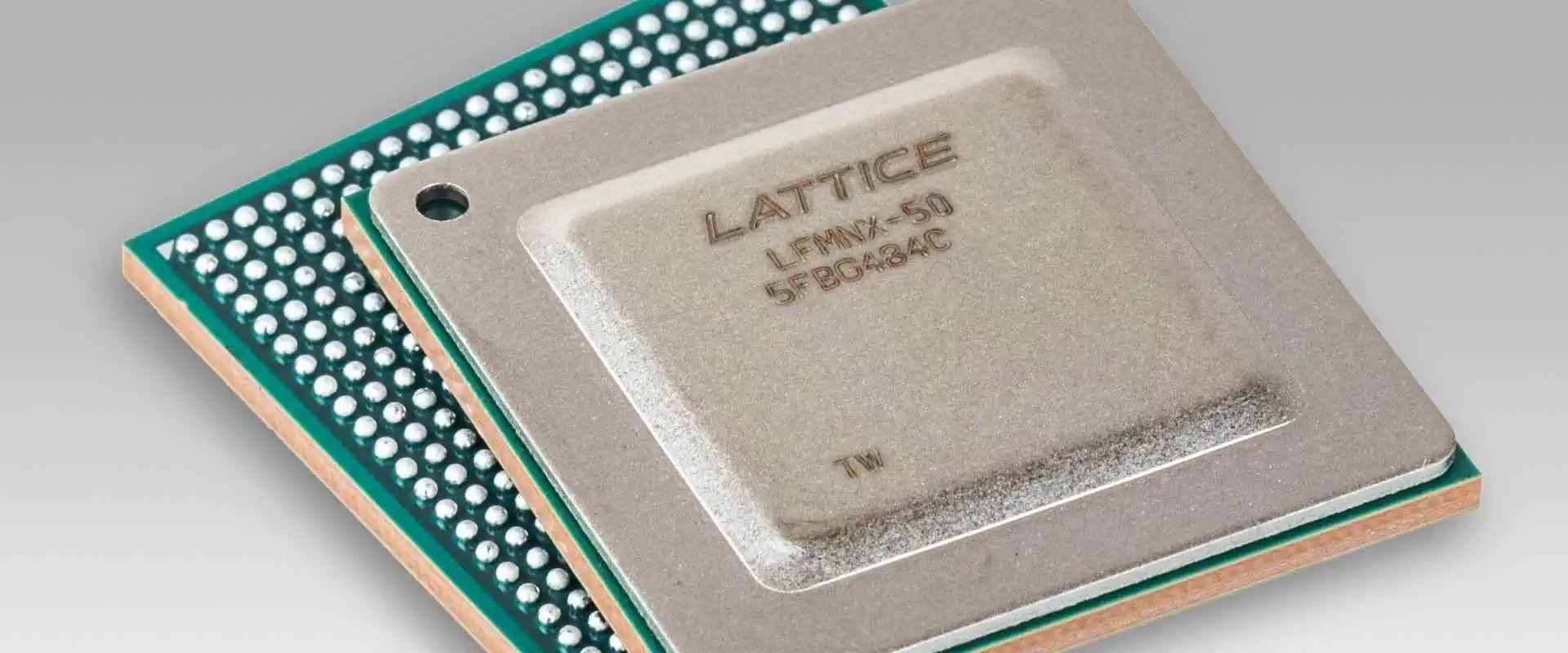
Lattice FPGA

Lattice Field-Programmable Gate Arrays (FPGAs) are a class of reconfigurable programmable logic devices we can set up for various tasks. For example, several industries use telecommunications, automotive, industrial control, medical, and the military.

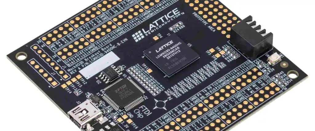
Lattice FPGAs are unique in their low power consumption, which makes them perfect for situations where power consumption is crucial. They are also appropriate for usage in applications with limited space because of their tiny form factor.

Hardware description languages (HDLs), such as Verilog and VHDL, can program Lattice FPGAs. Lattice FPGA designs are created, simulated, and implemented using the Lattice Diamond software suite. The software package consists of a GUI for entering designs, a compiler for turning designs into netlists, and a place-and-route tool for placing designs on FPGAs.

The built-in intellectual property (IP) blocks in Lattice FPGAs include memory controllers, high-speed transceivers, and DSP blocks, among others. These IP-building pieces can be incorporate into a design to simplify production

Several families of lattice FPGAs exist, each with distinctive features and abilities. The ECP5, MachXO3, and CrossLink-NX families of Lattice FPGAs are a few well-liked families.

Lattice FPGA Architecture

FULL PCB MANUFACTURING Quote

A global routing network links the programmable logic blocks (PLBs) in a hierarchy found in lattice FPGAs (GRN). Each PLB comprises a flip-flop and a customizable logic block (CLB) arranged in rows and columns. We implement the Boolean logic functions of the design by the CLB, which is the fundamental component of the FPGA. The flip-flop helps synchronize and store data.

Lookup table and multiplexer

A lookup table (LUT) and multiplexer comprise the CLB (MUX). The truth table of a Boolean function sits in the LUT, a programmable memory. We choose the output of the LUT or the input from the next CLB using the MUX. Carry chains are another feature of the CLBs for quick addition and subtraction operations.

GRN

Signals must be routed between the PLBs by the GRN. The inputs and outputs of the CLBs connect by a system of horizontal and vertical wires known as the GRN. Moreover, the GRN has programmable switches that the designer can use to link the PLBs in any pattern they like.

Dedicated resources

Furthermore, we can implement memory and arithmetic operations using specialized resources in lattice FPGAs. Specifically, designed blocks for implementing RAM, ROM, and DSP functions are among these resources. Furthermore, arranging the RAM blocks as single-port or dual-port memory is possible. Moreover, we can set up the ROM blocks. Finally, the implementation of arithmetic operations, including addition, subtraction, multiplication, and division, is optimized for the DSP blocks.

Clock management resources

Furthermore, clock management resources are provided by lattice FPGAs, enabling the designer to produce and distribute clocks throughout the system. These tools include delay-locked loops (DLLs) and programmable phase-locked loops (PLLs), which may produce clocks with various frequencies and phases. To ensure that the clock signals reach various components of the design simultaneously, the PLLs and DLLs can also be helpful for clock skew management.

High-speed serial interfaces

Moreover, Lattice FPGAs have resources set aside for implementing high-speed serial interfaces like USB, Gigabit Ethernet, and PCI Express. In addition, physical layer (PHY) circuits, serializers, and deserializes are resources that implement the interface’s electrical and low-level signaling requirements.

Configuration memory

Lattice FPGAs additionally have a configuration memory that houses configuration and design data. Many techniques can program the configuration memory, including JTAG, SPI, and a separate configuration bus. In addition, we can modify a piece of the FPGA without affecting the remainder of the design thanks to a configuration memory feature that enables partial reconfiguration of the FPGA.

Power management resources

Lattice FPGAs also provide several power management capabilities that the designer can use to lower the design’s power usage. These capabilities include low-power modes, which allow the FPGA to be put into a low-power state when not in use, and dynamic power management, which enables unneeded design components to turn off to save power consumption.

Programming Lattice FPGA

FPGAs are programmable devices to carry out particular functions or create digital circuits. FPGAs comprise a grid of programmable logic cells coupled with programmable routing resources. One of the top FPGA producers, Lattice Semiconductor, provides a broad selection of devices for various purposes.

Setting up the development environment

Xilinx Zynq fpga
Xilinx Zynq fpga

Lattice FPGA development environments needs setting up in several different ways. This is an overview:

Lattice Diamond software installation: Most FPGA development using Lattice devices uses this software. Follow the installation wizard after downloading it from the Lattice Semiconductor website.

Setup the cables for Lattice programming: You might need to add particular programming connections depending on your kind of Lattice FPGA. The Lattice Semiconductor website has the drivers and installation instructions.

Get your FPGA board ready: Use USB or another compatible interface to connect your FPGA board to your PC. To ensure it is powered on and connected correctly, adhere to the manufacturer’s instructions.

Make a new undertaking: Open a new project in the Lattice Diamond software. Choose your FPGA device from the list of compatible devices and adjust the project settings as necessary.

Put your VHDL or Verilog code here: Either write your code in Verilog or VHDL using the Lattice Diamond program. These are the two main programming languages for FPGAs.

Make a model of your design: Before synthesizing your design for the FPGA, test it using Lattice Diamond’s simulation tool.

Create a binary file that can be put onto the FPGA by synthesizing your design using the Lattice Diamond synthesis tool.

Configure your FPGA: The binary file produced in the preceding step should be used to program the FPGA using the Lattice programming tool included in Lattice Diamond.

After completing these procedures, your Lattice FPGA development environment should be completely operational.

Creating a new project

Creating a new project in Lattice Diamond is the initial step in programming a Lattice FPGA. A project, a collection of design files and configuration information, defines an FPGA design. Go to file ~, then New ~, then Project in Lattice Diamond, and choose the device family and type corresponding to your intended FPGA board to start a new project. Next, select the project’s name and location before clicking OK.

Adding design files to the project

The project needs to have design files added once we create it. This is because the source code for the FPGA design is in design files written in a Hardware Description Language (HDL) like Verilog or VHDL. By selecting Add Sources from the context menu when you right-click the project name in the Project Navigator in Lattice Diamond, we can add design files to the project.

Any text editor or integrated development environment (IDE), such as Xilinx Vivado or Quartus Prime, can be used to create design files. However, the behavior and functionality of an FPGA design depend on a top-level module that instantiates other modules or components.

Synthesizing the design

We must combine the design after adding the design files to the project. A netlist, an illustration of the FPGA architecture in terms of logic gates and flip-flops, is created through synthesis, which involves translating the HDL code into a netlist. The Lattice Synthesis Engine (LSE), a part of Lattice Diamond, is used for synthesis.

Choose Synthesize Design from the Process menu in Lattice Diamond to synthesize the design. The LSE tool will then start and analyze the HDL code to produce a netlist. Depending on the needs of the design, the LSE tool offers a variety of synthesis options, including optimization level, technology mapping, and clock domain analysis.

Implementing the design

We must put the design into practice when it synthesizes. Implementing the requested functionality involves mapping the netlist onto the FPGA architecture, configuring the programmable logic cells, and allocating resources. The Lattice Diamond Place-and-Route (P&R) tool is helpful for implementation, and it creates a bitstream file by mapping the netlist onto the FPGA design.

Choose Implement Design in Lattice Diamond’s Process menu to implement the design. Then, the Place-and-Route (P&R) tool will launch, mapping the netlist onto the FPGA architecture and creating a bitstream file.

The P&R tool performs several operations, such as placement, routing, and time analysis. The physical location of each logic cell on the FPGA depends on the placement. Routing entails configuring the interconnect resources to connect the logic cells following the netlist. Finally, by performing timing analysis, you can ensure the design complies with the timing specifications in the HDL code.

It’s crucial to set up the implementation settings correctly based on the design specifications during implementation. This entails picking the appropriate FPGA family and device, establishing the I/O restrictions, and defining the timing and power parameters.

Once the implementation is complete, the P&R tool creates a bitstream file with the FPGA configuration information. Then, the Diamond Programmer tool can download the bitstream file to the FPGA.

Programming the FPGA

Intel FPGA

Once the bitstream file is ready, you can download it to the target FPGA board to begin programming the FPGA. The Diamond Programmer tool, which supports various programming modes, including JTAG, SPI, and flash programming, can accomplish this.

Connect the target FPGA board to the computer via a USB cable, then start the Diamond Programmer tool to program the FPGA. First, choose the programming mode, then select the programming parameters to match the target FPGA board. The bitstream file will then be downloaded to the FPGA when you pick it and click program.

After programming, the FPGA will perform the desired functionality provided in the HDL code. We may rapidly prototype and develop FPGA designs since we can reprogram the FPGA as often as necessary.

Debugging the design

FPGA design must include debugging since it enables us to find and correct design flaws. Lattice Diamond offers several tools for debugging FPGA designs, including simulation, timing analysis, and waveform visualization.

Simulation entails simulating the HDL code with a simulator tool, such as ModelSim or Aldec Active-HDL. Before programming the FPGA, we can use simulation to evaluate the design’s functionality and find any problems or errors in the HDL code.

Timing analysis entails examining the design’s timing performance to ensure it complies with the timing specifications stated in the HDL code. Lattice Diamond offers a timing analyzer tool that enables us to examine the design’s timing performance and spot any timing inaccuracies.

Waveform watching entails utilizing a waveform viewer tool, such as Lattice Reveal, to observe the signals and data flow in the design. By inspecting the waveform, we can see how the design behaves and spot any problems or errors in the HDL code.

Application

Industrial application of Lattice FPGA

Lattice FPGAs are helpful in several industrial applications in numerous sectors. For example, lattice FPGAs are frequently essential in the following industrial applications:

Industrial Automation:

Lattice FPGAs are used in industrial automation to operate robots, monitor, and manage production processes, and set up machine vision systems, among other things. FPGAs are perfect for industrial automation applications with high-speed data processing and minimal latency since they provide real-time processing capabilities.

Communications:

To accomplish high-speed data transport, signal processing, and protocol conversion, communication systems utilize lattice FPGAs. Furthermore, FPGAs are employed in cable, optical, and wireless communication systems to increase performance and decrease delay.

Test and Measurement:

In test and measurement devices like oscilloscopes, signal analyzers, and network analyzers, lattice FPGAs are suitable. FPGAs are perfect for test and measurement applications that call for high precision and low latency because they can process data at high speeds and in real time.

Energy:

Energy applications include the monitoring and control of energy distribution networks, the implementation of energy management systems, and the control of power-producing systems. FPGAs are perfect for building energy-efficient systems since they have a high performance to low-power consumption ratio.

Medical:

Lattice FPGAs are helpful in medical applications to interpret medical imaging data, monitor vital signs, and control medical equipment. FPGAs are perfect for medical applications requiring real-time processing and low energy usage due to their high performance and low power consumption.

Aerospace and Defense:

Lattice FPGAs are helpful in aerospace and defense applications for various functions, including managing radar, missile guidance, and avionics systems. FPGAs are perfect for aerospace and defense applications that demand robustness and endurance in severe environments because of their high dependability and radiation tolerance.

Automotive application of Lattice FPGA

There are numerous uses for lattice FPGAs in the automobile sector. For example, lattice FPGAs are frequently essential in the following automotive applications:

Advanced Driver Assistance Systems (ADAS):

For purposes like object identification, lane departure warning, and collision avoidance, lattice FPGAs are helpful in ADAS. In addition, FPGAs are perfect for ADAS applications that need high-speed data processing and minimal latency since they have real-time processing capabilities.

Engine Management Systems:

Lattice FPGAs are helpful in engine management systems to regulate the timing of the ignition, fuel injection, and other aspects of the engine. FPGAs are perfect for building intricate engine control systems because of their high performance and low power consumption.

In-Car Infotainment Systems: 

Lattice FPGAs are helpful in in-car entertainment systems to perform audio processing, video decoding, and user interface control. FPGAs are the best choice for incorporating cutting-edge infotainment features in contemporary vehicles because they combine great performance and low power consumption.

Head-Up Displays (HUDs):

HUDs use lattice FPGAs to project critical driving data onto the windscreen, such as speed, directions, and safety alerts. FPGAs are perfect for implementing advanced HUD features because they provide real-time processing and high-resolution graphics capabilities.

Tire Pressure Monitoring Systems (TPMS):

To monitor tire pressure and identify probable tire failures, TPMS uses lattice FPGAs. FPGAs are perfect for constructing TPMS systems that constantly run without depleting the car’s battery because they have high data processing speeds and little power consumption.

Adaptive Lighting Systems:

Adaptive lighting systems use lattice FPGAs to change the headlights according to speed, weather, and kind of road. FPGAs are perfect for building sophisticated lighting control systems that increase driver safety and visibility since they have real-time processing capabilities.

Vehicle-to-Vehicle (V2V) and Vehicle-to-Infrastructure (V2I) Communications:

Vehicle-to-vehicle and vehicle-to-infrastructure communication are possible using lattice FPGAs in V2V and V2I communication systems. In addition, FPGAs are perfect for building real-time communication systems that can increase traffic safety and efficiency because they provide high-speed data processing and low latency.

Consumer electronics application

Lattice FPGAs’ excellent performance, low power consumption, and flexibility make them useful in various consumer electronics applications. For example, lattice FPGAs are frequently helpful in the following consumer electronics applications:

Mobile Devices:

Mobile devices use lattice FPGAs to process audio and video, manage batteries, and process sensor data. FPGAs are perfect for incorporating sophisticated features in mobile devices while preserving battery life because they combine great performance with low power consumption.

Gaming:

For activities like audio and video processing, user interface control, and picture identification in gaming applications, lattice FPGAs are helpful. FPGAs are perfect for integrating sophisticated gaming features and enhancing user experience since they provide real-time and high-speed data processing capabilities.

Virtual and Augmented Reality:

In virtual and augmented reality systems, lattice FPGAs are helpful for operations like image and video processing, sensor data processing, and user interface control. In addition, FPGAs are perfect for integrating real-time virtual and augmented reality features because of their high performance and low latency.

Audio and Video Processing:

Applications for audio and video processing, including soundbars, smart speakers, and video streaming devices, utilize lattice FPGAs. FPGAs are perfect for integrating advanced audio and video processing features while reducing energy usage since they have excellent performance capabilities and low power consumption.

Robotics and Drones:

Robotics and drone applications use lattice FPGAs for sensor data processing, navigation, and control. FPGAs are perfect for creating complicated robotic and drone systems since they have tremendous performance capabilities and consume less power.

Home Automation:

Applications for home automation use lattice FPGAs to interpret sensor data, manage connected devices, and develop voice assistants. FPGAs are the best choice for building power-efficient home automation systems because of their excellent performance capabilities and low power consumption.

Wearable Devices:

In wearable technology, lattice FPGAs are suitable for battery management, user interface control, and sensor data processing. In addition, FPGAs are perfect for building wearable technology that can run continuously for a long time because they have excellent performance capabilities and use little power.

How to set up, connect and configure Mister FPGA on devices

Mister FPGA

Mister FPGA’s hardware and software project aims to use an FPGA chip to simulate the operation of vintage video game consoles, PCs, and arcade machines.

The hardware platform offered by the project consists of an FPGA board called the “Mister” board and several add-on boards that support various systems. The FPGA may then execute software as if it were the original hardware by having users load “cores” of software that mimic the hardware of a particular console or computer.

Mister FPGA accurately simulates the original hardware at a low level. As a result, it makes it a very accurate way to operate vintage computing systems and play classic games. The FPGA architecture also makes it possible to design new cores. As a result, enthusiasts can add to the system to support different devices. As a result, the project has a sizable fan base among retro gaming fans and has emerged as a preferred method of enjoying vintage video games and computing devices.

YouTube video

Why Mister FPGA is a popular alternative to classic consoles

Mister FPGA PCB Board

Mister FPGA is a well-liked substitute for vintage consoles for several reasons:

Accuracy: Mister FPGA accurately reproduces the hardware of vintage consoles, PCs, and arcade games. This results in an accurate and true experience because software operating on the Mister platform behaves like running on the original hardware.

Versatility: The Mister FPGA platform supports various devices, including arcade machines, retro computers like the Amiga and Atari ST, and old consoles like the NES and Sega Genesis. Users can have a single device that can simulate a variety of systems thanks to its adaptability.

Preservation: It’s getting harder and harder to find vintage video games, computers, and arcade devices because manufacturers are no longer manufacturing them. Users that use Mister FPGA can use old software and play games without the requirement for the original hardware, protecting these systems for future generations.

Users can highly customize Mister FPGA, who can add their own “cores” to the system that simulate various hardware systems. But, of course, this implies that we can enhance the platform to enable additional features and systems.

Comparison to software emulation and hardware clones

Compared to Mister FPGA, two other standard methods for playing old games and using historical computing systems are software emulation and hardware clones, each of which has pros and cons.

Software emulation

Emulating software is the technique of running software on a current device. It mimics the hardware of a retro console or computer. Without the need for original hardware, users can play retro games and use vintage software by downloading and installing emulator software. One of the key benefits of software emulation is that we can install it on any contemporary device, which is frequently free or inexpensive.

However, software emulation might have accuracy problems because emulators might not accurately reproduce the original hardware. As a result, it can cause hiccups or inconsistencies in the functionality or gameplay. Furthermore, software emulation demands a lot of computing power. Additionally, the host device’s performance can affect how well the emulation performs.

Hardware clones

On the other hand, hardware clones are actual objects created to use contemporary parts to mimic the functionality of vintage consoles or computers. As a result, software emulation generally lacks the authenticity of hardware clones, frequently made to appear and feel like the original gear. Furthermore, hardware clones can frequently offer a more reliable and accurate experience than emulation because they are not dependent on the host device’s processing capability. Clones of the original hardware, however, might be pricey and may not be able to accurately recreate it, which could cause compatibility problems or flaws in the gameplay or functioning.

Mister FPGA has several benefits over hardware clones and software emulation. First, because Mister FPGA closely mimics the original hardware at a basic level, it offers a very accurate approach to operating vintage computing systems and playing classic games. This results in an accurate and true experience because software operating on the Mister platform behaves like running on the original hardware. Moreover, Mister FPGA offers customers a flexible platform that can imitate a variety of devices, including a wide range of systems, from ancient PCs to classic consoles.

Second, Mister FPGA offers an incredibly configurable platform. Users can add their own “cores” to the system, which simulate various hardware systems. This implies that the platform can handle new systems and features, offering a flexible platform for old-school video games and computer fans.

Moreover, because Mister FPGA is a single device that can imitate numerous distinct systems, it offers a very portable platform. This allows customers to take the Mister FPGA wherever they go and offers a practical method to play retro games and use old computing platforms.

Setting up Mister FPGA on a computer

FULL PCB MANUFACTURING Quote

Setting up Mister FPGA on a computer can be challenging, but we can do it in several simple steps. The following is a general setup guide for Mister FPGA on a computer:

Step 1: Choose Your Hardware

Selecting the hardware for your Mister FPGA setup is the first step. The DE-10 Nano and the IO Board, the suggested hardware elements for Mister FPGA, are just two choices. Once you have the necessary hardware, you must assemble the parts and ensure they are linked correctly.

Step 2: Download the Required Software

We must download the essential software for Mister FPGA next. Both the SD card image, which contains the operating system and software necessary to run the Mister FPGA system, and the Mister FPGA core, which is the software that emulates the hardware of the console or computer you want to use, are included in this.

Step 3: Write the SD Card Image

After downloading, you must use software like Etcher or Win32DiskImager to write the SD card image to an SD card. The SD card will include the software and operating system needed to run Mister FPGA.

Step 4: Configure the FPGA Core

The FPGA core must then run to simulate the hardware of the desired console or computer. To accomplish this, you must download the core file and copy it to the SD card. Next, we must configure the core parameters by editing the INI file on the SD card. The configuration options for the core stay in a text file called an INI file.

Step 5: Connect to a Monitor or TV

You can use an HDMI connection to link your Mister FPGA setup to a monitor or TV once you’ve written the SD card image and set up the FPGA core. A USB keyboard and mouse can also be helpful with the configuration of input devices.

Step 6: Power Up and Test

Your Mister FPGA system can now be powered on and tested. As the setup starts, the Mister FPGA menu should appear, allowing you to choose the console or computer you want to emulate. Once ROMs or software load onto the system, you can use old software or play video games.

It is crucial to remember that installing Mister FPGA can be complicated, and you might need to take extra steps depending on the specific hardware you’re using and the console or computer you wish to simulate. Therefore, adhering to comprehensive setup instructions and guides is advised to guarantee a successful setup. Also, confirming that any ROMs or software utilized with Mister FPGA were bought legitimately and did not break copyright regulations is critical.

Connect Mister FPGA to a display and input devices

Due to its ability to replicate the original hardware’s architecture, circuitry, and behavior, Mister FPGA offers customers an experience comparable to real hardware.

You will need to adhere to a set of instructions to link Mister FPGA to an input device and a display.

Required Equipment

Before we begin, you will need to gather the following equipment:

  • Connecting the Display
  • USB game controller
  • USB keyboard
  • HDMI cable
  • Mister FPGA board

Connecting Mister FPGA to a display is the initial stage in the connection process. Follow these steps to accomplish this:

  • On the Mister FPGA board, find the HDMI port. It often sits on the board’s side.
  • Attach one end of the HDMI cable to the Mister FPGA board’s HDMI port.
  • Attach the HDMI cable’s other end to a display device, such as a TV or monitor with an open HDMI port.

When you attach the HDMI wire, the Mister FPGA’s menu should appear on your screen.

Connecting Input Devices

It’s time to connect your input devices now that the display is linked. Many input devices, such as USB keyboards and game controllers, are supported by Mister FPGA. Here’s how to link them together:

  • Discover where your Mister FPGA board’s USB ports are. On the side of the board, there usually are two or more ports.
  • Join your USB keyboard to a port that is accessible.
  • Attach your USB game controller to a different USB port that is accessible.

With your input devices linked, you should be able to use them to play games and browse the menu on the Mister FPGA.

Configuring Input Devices

By default, Mister FPGA should be able to detect your input devices and let you use them to play games and explore the menu. But, if your input devices malfunction, you might need to adjust them. Here is how you do it:

  • Open the Mister FPGA menu and select the Input option.
  • Choose the gaming controller or keyboard as the device you want to set up.
  • To configure your device, adhere to the on-screen instructions.

After configuring, you should be able to utilize your input devices to play games.

Troubleshooting

Here are some troubleshooting techniques to try if your Mister FPGA is giving you problems:

Examine your connections. Ensure your Mister FPGA board correctly connects to all cables and input devices.

Verify the display’s settings: Confirm that the input source and resolution are set appropriately on your monitor.

Confirm the settings on your input device: Make sure the Mister FPGA menu configures your input devices correctly.

Get a firmware update: If there are any available firmware updates, check the Mister FPGA website.

If none of these measures fix your problem, you might need to look for more information on Mister FPGA in the documentation or forums.

Mister FPGA Cores

Intel OpenCL FPG

We can create a hardware-based FPGA board as part of the well-known open-source project Mister FPGA. Additionally, we can configure it to simulate a variety of vintage game consoles, computers, and arcade machines. The Mister FPGA board presents an FPGA chip that can act like the original hardware of several vintage game consoles, computers, and arcade machines. Retro gaming enthusiasts love the Mister FPGA project because it lets them play their favorite games with improved visuals and sound on modern hardware.

The fact that Mister FPGA offers a more precise simulation of vintage hardware than software emulators is one of its most essential features. This is so that FPGA hardware can more accurately simulate the behavior of the original hardware than software. As a result, Mister FPGA offers a more realistic vintage gaming experience than conventional software emulators, with better visuals and sound.

Each Mister FPGA core emulates a distinct vintage game console, computer, or arcade equipment.

Amiga core

Commodore introduced the Amiga range of personal computers in the middle of the 1980s. It was renowned for having cutting-edge graphics and audio capabilities and an operating system supporting several tasks simultaneously. As a result, the Amiga was widely utilized in the demo scene and among fans of video production and games.

New Amiga cores have been created and distributed over the years by various businesses and people, including FPGA implementations that can be helpful with hardware like the MiSTer and FPGA Arcade boards. These cores seek to bring new features and capabilities while faithfully recreating the original Amiga hardware.

The Minimig and its offshoots are some of the more well-known Amiga cores. These cores preserve the history of this legendary computer system while enabling Amiga users to use vintage Amiga applications on contemporary hardware.

The MiSTer emulates the Amiga 500 and Amiga 1200 computers and the AGA core emulates the Amiga 1200 and Amiga 4000 computers with AGA (Advanced Graphics Architecture) chipset, are only a few Amiga cores that are available for FPGA platforms.

Arcade cores

Several arcade cores are also included in Mister FPGA, enabling users to simulate vintage arcade devices. These cores, which imitate arcade machines made by Capcom, SNK, and other manufacturers, include the CPS1, CPS2, and Neo Geo cores. The Mister FPGA arcade cores deliver a genuine experience with improved visuals and sound.

On the MiSTer platform, numerous arcade cores are available, including well-known games like Pac-Man, Donkey Kong, Galaga, and Street Fighter II. In addition, specific arcade cores also allow for online multiplayer gaming, enabling online multiplayer competition between participants.

Arcade cores on the MiSTer platform provide several advantages over conventional arcade cabinets. They include the convenience of playing numerous games on a single device and the option to record high scores and game progress.

Atari 2600 core

The hardware in the original Atari 2600 game machine emulates software in the Atari 2600 core for the MiSTer FPGA. “FPGA” refers to a class of integrated circuits that may be built and programmed to function as any digital circuit. The MiSTer FPGA can replicate several vintage gaming consoles, including the Atari 2600.

The MiSTer FPGA’s Atari 2600 core tries to properly reproduce the experience of playing vintage Atari 2600 games. It replicates the console’s input and output mechanisms, CPU, graphics, and sound hardware. This implies that you may play classic Atari 2600 games on a MiSTer FPGA using the same controllers and enjoying the same graphics and music as you would on the original console.

Overall, the MiSTer FPGA’s Atari 2600 core is an excellent method to play vintage Atari 2600 games on contemporary hardware. In addition, it has the added advantages of better video output and the choice to utilize contemporary controllers.

Commodore 64 core

The MiSTer FPGA’s Commodore 64 core is a hardware implementation of the iconic home computer. Fans of the storied machine will enjoy an authentic computing experience thanks to its goal of perfectly replicating the capabilities of the original hardware.

The core supports many Commodore 64 programs, such as games, demos, and productivity tools. It fully implements the MOS Technology 6510 CPU, the VIC-II graphics chip, and the SID sound chip from the original Commodore 64 computer.

240p, 480p, and 720p are just a few video output types the core can handle. In addition, various customization options enable users to personalize settings, including the display mode, audio output, and input mappings.

Game Boy core

The hardware implementation of the original Game Boy console on an FPGA board is the Game Boy core of the MiSTer FPGA. Fans of the vintage system will enjoy a realistic gaming experience thanks to its goal of perfectly replicating the original hardware’s functionality.

MiSTer’s Game Boy core supports original Game Boy and Game Boy Color games. It combines software and hardware emulation to mimic the original console’s capabilities. An FPGA implements the core’s hardware emulation. As a result, it allows for incredibly accurate timing and synchronization with the original hardware.

Fast forward, cheat codes and save states are core-supported functions. Also, it supports a variety of video output options, such as 240p, 480p, and 720p.

The versatility of the MiSTer FPGA platform is one of its main benefits. By changing options such as the display mode, audio output, and input mappings, users can tailor the core to their specific requirements. Updates and community contributions can also add new features and enhancements to the core.

For those who want a top-notch, authentic gaming experience and are specialists in the original console, the Game Boy core in the MiSTer FPGA is a fantastic choice.

Mega Drive/Genesis core

One of the most well-liked Mister FPGA cores is the Mega Drive/Genesis core, which reproduces the well-known Sega Mega Drive and Genesis consoles introduced in 1988. It offers a more realistic representation of the original hardware than software emulators, creating a more genuine retro gaming experience. In addition, the core can output video at various resolutions and supports both PAL and NTSC video modes.

Also, it offers support for several add-ons and extras, including the Sega CD and Sega 32X. The core also offers a variety of customization options. It enables users to adjust numerous parameters to get the look and feel they want. And last, it supports a variety of homebrew games and demonstrations that let users enjoy fresh content on retro hardware. As a result, it extends the usefulness and allure of the platform.

How the community contributes to the development of Mister FPGA

Creating software

Creating and disseminating software for the platform is one way the community helps Mister FPGA develop. Many community members produce software that runs on top of the FPGA chip’s core software, which the project’s maintainer develops. For instance, people have developed custom firmware for the system, which enhances compatibility with particular games or platforms and adds new capabilities. Others have developed tools for organizing game ROMs or designing unique platform combinations.

Testing and reporting

The testing and reporting of software issues is another way the community aids in developing Mister FPGA. Anyone can download and test the program on their hardware because Mister FPGA is open-source. As a result, users can discover flaws and submit them for the project’s maintenance to fix. In addition, the neighborhood contributes to testing updated hardware or new features to ensure they function correctly.

Hardware

In addition, the community contributes to the growth of Mister FPGA by developing platform hardware upgrades. For example, the Mister FPGA board contains several ports connecting accessories and peripherals, including HDMI, USB, SD card, and more. In addition, community members have enhanced the platform’s capabilities by developing add-on boards. For example, they include a VGA output board or an audio expansion board. These additions may boost the platform’s functionality, bring fresh features, or enhance system compatibility.

Promotion

In addition to these donations, the community aids with Mister FPGA’s promotion and acceptance. For example, many community members discuss their interactions with the platform in social media, forums, or blogs. As a result, it might draw new contributors and users. In addition, the platform’s learning curve can shorten. Additionally, it can be more accessible to the community, producing videos, guides, and documentation to assist new users.

Financing

Financial assistance from the public also helps the growth of Mister FPGA. Despite being open-source and cost-free, the project still has to pay to develop its hardware and software. The project’s manager can use community donations to buy hardware, cover hosting expenses, or pay developers to work on the project. Some community members even market their hardware upgrades for the system, which can bring in money for the endeavor.

Feedback

Finally, the community helps Mister FPGA improve by offering the project’s maintainer feedback and suggestions. The platform is user-driven. Therefore the maintainer frequently considers suggestions from users when selecting what features or systems to add next. In addition, the public can recommend new features, report bugs, or offer comments on already-existing features.

Conclusion

Connecting Mister FPGA to a display and input devices is rather simple. You should be able to start using Mister FPGA immediately by following the instructions in this guide. After your gear is linked, you may begin perusing the extensive collection of vintage gaming consoles, computers, and arcade machines that Mister FPGA supports.

Whizzing Through the World of RF and Microwave Engineering

Microwave Engineering

A world of RF and microwave engineering awaits you; are you up for the challenge? The newest technology combines various engineering disciplines in this fascinating sector. Navigating the rules of the microwave engineering world is no easy task, from eliminating interference to developing devices that can sustain high power levels. However, you can overcome these challenges and produce some of the most cutting-edge technology now on the market if you have the necessary knowledge and abilities. Furthermore, you can use RF, microwave, and AI technology to develop, improve, and maintain the systems that power the modern world. Thus, if you’re up for being a microwave engineer, get ready to explore this world of exciting engineering possibilities.

YouTube video

RF and Microwave Engineering: Definition

The RF (Radio Frequency) and Microwave engineering refer to the study and use of electromagnetic waves with frequencies ranging from a few kilohertz to hundreds of gigahertz. RF engineering frequently works with frequencies between 3 kHz and 300 GHz. This range covers programs like satellite communication systems, radio communication, television broadcasting, radar systems, and wireless networks. Frequencies between 300 MHz and 300 GHz are the focus of microwave engineering. This range covers programs like radar systems, microwave ovens, medical imaging devices, and microwave communication.

RF and microwave engineering studies antennas, transmission lines, microwave circuits, microwave devices, and electromagnetic interference. Circuit analysis, signal processing, and electromagnetic theory are all disciplines that call for in-depth knowledge. Engineers specializing in RF and microwave technology create, develop, and test high-frequency electronic parts and systems. They are responsible for ensuring these systems work effectively, perform as expected, and adhere to all applicable regulations. They design and test these systems using specialized software tools and techniques and collaborate closely with other engineers, technicians, and scientists to create new technologies and goods.

Requirements to Become a Microwave Engineer

RF Engineering
RF Engineering

To become a microwave engineer, there are specific requirements that you need to meet. The following are some of these requirements:

1. Extensive experience in electronics and engineering:

A solid foundation in engineering and electronics is necessary to become a microwave engineer. The implication is that you should hold a bachelor’s or master’s degree in electrical engineering or a closely related discipline. Also, you should have a vast knowledge of fundamental electronics concepts, such as electromagnetic theory, circuit analysis, and signal processing.

In addition, it is critical to have a firm understanding of electrical engineering because microwave engineering relies heavily on the fundamental ideas of the discipline. For example, wave propagation, transmission lines, and antenna theory are all things you ought to be knowledgeable about. Also, it would help if you could use software programs frequently employed in the microwave business, such as MATLAB, Ansys HFSS, and CST Microwave Studio.

2. Comprehensive understanding of microwave hardware and support systems:

Microwave engineers employ various tools and systems, such as microwave generators, amplifiers, filters, and antennas. Therefore, you must have a solid knowledge of these elements and how they relate to one another to succeed in this industry.

It would help if you were conscious of various microwave circuits, including waveguides, microstrips, and coaxial cables. In addition, you should be knowledgeable about microwave measurement methods, such as time-domain reflectometry (TDR) and vector network analysis (VNA).

Microwave engineers focus on support systems such as power supplies, cooling systems, and control electronics. You, therefore, ought to be familiar with these systems and how microwave apparatus incorporates them.

3. Strong problem-solving abilities:

Solving problems is a big part of microwave engineering. The design and development of microwave components and systems will provide several technological obstacles to you. Therefore, you must be adept at solving problems to succeed in this industry.

You should be able to deconstruct complicated issues and devise original fixes. Also, you should be able to address difficulties both individually and collaboratively.

4. High levels of interpersonal and communicative ability:

In addition to other engineers, scientists, and project managers, microwave engineers collaborate with various individuals. Therefore, it would be best to have excellent communication and interpersonal skills to succeed in this area.

The ability to clearly and concisely convey complex technical knowledge to non-technical persons is necessary. With these skills, you should work cooperatively with others and be receptive to criticism and advice.

5. Design evaluation:

Designing and creating microwave systems and components is the responsibility of microwave engineers. You must be able to analyze designs to be successful in this industry.

Using simulation tools and measurement methodologies, you should be able to evaluate the performance of microwave components and systems. Also, you should be able to pinpoint potential improvement areas and suggest design changes.

Challenges Youโ€™re Likely to Encounter as a Microwave Engineer

FULL PCB MANUFACTURING Quote

Microwave engineering is a challenging field involving designing, developing, and applying microwave components and systems. As a microwave engineer, you may run into various technical problems needing creative fixes. As a microwave engineer, you will likely face the issues listed below:

1. Overcoming interference:

Interference is among the main problems microwave engineers have to deal with. Radar, navigation, and communication systems are just a few of the applications that use microwave frequencies. As a result, there is a high chance of interference between various systems using nearby frequencies. Therefore, microwave engineers must create components with high selectivity and low insertion loss and apply sophisticated filtering methods to overcome interference. To ensure compliance, they must know the frequency allocation rules and cooperate closely with regulatory organizations.

2. Creation systems that can withstand high power levels:

Many technological difficulties may arise because microwave systems frequently operate at high power levels. Components may overheat, deteriorate, or stop working at high power levels. In addition, strong electromagnetic fields can produce undesirable outcomes, including radiation and arcing. Microwave engineers must carefully choose components suitable for high-power applications to create systems that can manage these amounts of power. Also, they need to develop parts with great power-handling capacities and apply sophisticated cooling strategies. Finally, they must be knowledgeable about safety laws and work closely with regulatory organizations to ensure compliance.

3. Addressing the impact of temperature variations on system performance:

Microwave system performance can significantly vary due to temperature variations. For instance, a component’s electrical characteristics may degrade due to temperature variations that cause it to expand or contract. Furthermore, temperature variations may impact the thermal stability of components, which may result in modifications to their performance over time. Microwave engineers must, therefore, carefully choose components that function over a wide temperature range to deal with the impacts of temperature variations. To keep component temperatures within acceptable bounds, they must also use sophisticated thermal management techniques, such as heat sinks and thermoelectric coolers.

4. Keeping the system’s dependability:

Microwave systems frequently apply in crucial applications, including communication, navigation, and military systems. Therefore, these systems must be highly dependable and upgradeable. To preserve system reliability, microwave engineers must incorporate fault-tolerant and redundant elements into their designs. They also need to employ cutting-edge testing methods to spot probable failure modes before they happen, like accelerated life testing and environmental stress screening.

5. Ensuring compliance with regulations:

Frequency allocation, safety, and environmental laws are only a few regulations that apply to microwave systems. To achieve compliance, microwave engineers must comply with these rules and work closely with the relevant authorities.

Microwave engineers must create systems that meet or surpass regulatory criteria to ensure compliance with regulations. To prove compliance, they must also employ cutting-edge testing methods, including safety and electromagnetic compatibility.

Career Opportunities in Microwave Engineering

materials for microwave PCB

Designing, creating, and using microwave systems and components is the focus of the highly specialized subject of microwave engineering. The following are some of the job options in microwave engineering:

1. Development and Research:

Research and development are significant areas for employment in microwave engineering. Microwave engineers in this industry collaborate in teams to develop new technologies and products. New systems and components are easy to design using a variety of modeling and simulation approaches and assess their performance through thorough testing. As a result, the microwave engineering sector needs research and development to expand and flourish. Manufacturing medical equipment, telecommunications, aerospace, and defense are just a few fields where engineers engaged in research and development can find employment.

2. Technology in Telecommunications:

Microwave engineers have a lot of job options in the telecommunications sector. Microwave communication system design and execution are the responsibility of telecommunications engineers. Examples of these systems are cellular networks, satellite communication systems, and point-to-point microwave links. A telecommunications engineer’s job is to make sure the communication systems are dependable, effective, and satisfy the expectations of their users. Governmental organizations, equipment manufacturers, and telecom service providers employ telecommunications engineers.

3. Engineering in Aerospace:

Microwave engineers have many employment options in the aerospace business. Engineers in this field create and build microwave systems for aircraft applications like communication, Radar, and navigation systems. Aerospace engineers find employment in commercial and government aerospace companies and research institutions. Since the aerospace sector constantly expands, new technologies and ideas are always in demand.

4. Military Engineering:

A substantial employment opportunity for microwave engineers is in defense engineering. Engineers in this sector design and build microwave systems for military applications, including Radar, communication, and electronic warfare systems. Defense engineers find employment in defense firms, governmental bodies, and academic institutions. Engineers must have robust talent, knowledge, and creativity to succeed in the stressful area of defense engineering.

5. Engineering Medical Devices:

A relatively emerging area of microwave engineering is the production of medical equipment. In this sector, engineers create microwave systems for imaging and surgical equipment, among other medical uses. Microwave engineers are in greater demand in the medical equipment industry as manufacturers use microwave technology in their products more frequently. Therefore, medical equipment design and microwave technology require a deep understanding of microwave engineers working in the manufacturing industry.

Current Trends in the Field of Microwave Engineering

RF Hardware Engineer

With the introduction of new technologies and trends, the field of microwave engineering is continually developing. Microwave engineering is experiencing a massive change due to recent advancements in technology. The following are these technologies discussed in detail:

1. The application of artificial intelligence (AI):

Microwave engineering is one of the many fields transforming due to the quickly expanding science of artificial intelligence. AI can accomplish automation of microwave components and system design and optimization. Engineers can use AI algorithms to determine which microwave systems and parts are most effective for a given application. AI can also help continuously improve the performance of microwave systems. AI also helps enhance the security of microwave communication systems by spotting and thwarting cyber-attacks.

2. Internet of Things (IoT):

Another development reshaping the microwave engineering industry is the Internet of Things. IoT refers to connecting numerous machines and things to the Internet so they may communicate and exchange data. IoT is now applicable in microwave engineering to connect microwave devices to the Internet, enabling in-flight monitoring and management of microwave systems. Additionally, IoT helps automate the testing and certification of microwave systems.

3. Big Data:

We use big data to refer to the massive amounts created by various systems and devices. Big data is now applicable in microwave engineering to enhance microwave components and system design and optimization. Engineers who use big data analytics to analyze microwave data can better understand patterns and trends that will help them improve the operation of microwave systems. Furthermore, Big data has now enhanced the effectiveness and dependability of microwave communication systems.

4. 5G:

5G is the fifth generation of wireless communications. By enabling quicker, more dependable, and more effective wireless communication, it is likely to transform the field of microwave engineering. In addition, since 5G networks use higher frequency bands than older wireless technologies, they can move more data faster. In microwave engineering, 5G is helping create brand-new microwave communication systems that can sustain the high-speed data transfer demanded by contemporary applications like virtual reality, augmented reality, and self-driving automobiles.

5. Autonomous Robots:

Autonomous Robots are robots that can complete tasks without human involvement. For example, installing, testing, and maintaining microwave communication networks is the work of autonomous robots in microwave engineering. In addition, these robots can hold cameras and sensors to explore and examine microwave systems. To reduce the need for human interaction, autonomous robots can also help automate the testing and validation of microwave systems.

6. Blockchain:

We define blockchain as a distributed ledger technology that makes transactions safe and open. Blockchain technology is applied to microwave engineering to improve the trustworthiness and security of microwave communication networks. By generating an unchangeable record of every transaction, blockchain can quickly secure the validity and integrity of microwave data. It can also help build a secure, decentralized network that guards against illegal access to microwave communication networks.

Conclusion

In conclusion, microwave engineering requires familiarity with various subjects, including electromagnetic theory, circuit analysis, signal processing, and antenna design. Furthermore, new technologies like 5G, big data, and AI are changing how microwave engineers design and develop microwave systems, making it a fascinating profession constantly evolving. Additionally, more and more job possibilities are opening up in the specialist field of microwave engineering as technology advances. Hence, if you’re looking for a means to make the most of your education and skills, a career in microwave engineering might be ideal for you.

Understanding the architecture and application of Xilinx Zynq

Xilinx Zynq

The design process for Xilinx Zynq

The Xilinx Zynq System-on-Chip combines an ARM Cortex-A9 dual-core processor with programmable logic fabric and is a flexible and high-performance gadget. A detailed understanding of the device architecture and the design tools and processes offered by Xilinx is necessary for designing a system around the Zynq SoC.

System Requirements and Architecture Design

Determining the needs and architecture of the system is the first stage in developing a system around the Zynq SoC. This entails specifying the high-level architecture of the system as well as the individual functionality and performance requirements that the system must meet. Suppose the system is a video processing programme, for instance. In that case, the requirements can include the capacity to handle high-resolution video at a particular frame rate and support for several video formats.

The architecture design process comprises choosing the proper hardware and software components to achieve the system requirements. This may involve determining the number and kind of peripherals, such as Ethernet, USB, or HDMI interfaces, that will be necessary for the instance of the Zynq SoC. Moreover, the right ARM Cortex-A9 processor configuration, including the core count and clock speed, may need to be chosen.

YouTube video

Hardware Design

xilinx zynq 7000
xilinx zynq 7000

A system-on-chip (SoC) called Xilinx Zynq combines a customizable logic fabric with an ARM-based processing system. As a result, high levels of integration and flexibility are made possible in embedded system designs.

There are a few crucial procedures to take while designing hardware for Zynq:

Determine the system’s requirements: The requirements must be clear before any hardware design can start. This includes elements like performance, power use, and I/O specifications.

Select the right Zynq device: Xilinx provides a variety of Zynq devices with varying processing capabilities and levels of integration. Choose the device that best fulfills the system specifications.

Create the processing system: Zynq’s system may use Xilinx’s Vivado software. Configuring the ARM processors, memory interfaces, and other system-level components falls under this category.

Create the programmable logic fabric: The programmable logic fabric may also result from Xilinx’s Vivado software. This entails creating the digital circuits that will be helpful in the FPGA.

Link the processing system and the programmable logic fabric: After the processing system and the programmable logic fabric are ready, they must be linked. The AXI bus interface is commonly essential for this.

Test and debug the design: It is critical to properly test and debug the design before deploying it in a real system. We can accomplish this with Xilinx’s Vivado software and external test equipment.

Ultimately, creating hardware for Zynq necessitates a thorough knowledge of hardware and software design concepts. In addition, it is critical to properly prepare and test the design at each stage to verify that it fits the system requirements.

Software Design

The software element of the system must be available in addition to the hardware. This entails choosing an appropriate operating system (such as Linux or FreeRTOS) and designing software programs to operate on it.

Because Xilinx Zynq devices mix programmable logic with an ARM-based processing engine, software design is essential for working with these devices. Following are some significant phases in the Zynq software design process:

Choose an appropriate operating system: The Zynq may run various operating systems, including Linux, FreeRTOS, etc. Choose the operating system that best meets the needs of the system you are developing.

Create processing system software: Zynq’s processing system incorporates one or more ARM processors that we can program using common development tools and languages, including C, C++, and Python. Develop software that runs on ARM processors and performs system-level functions.

Create software for the programmable logic fabric: we may also program Zynq’s programmable logic fabric with high-level synthesis tools like Xilinx’s Vivado HLS. Finally, create software to do bespoke digital signal processing, acceleration, or other operations on the programmable logic fabric.

Link the processing system to the programmable logic fabric: You’ll need to develop an interface utilizing Xilinx’s AXI bus or another protocol to enable communication between the software running on the processing system and the programmable logic fabric.

Test and debug the software: As with hardware design, extensively test and debug the software running on the Zynq. This is possible using regular debugging tools and procedures.

Improve performance and power consumption: Zynq devices are extremely flexible and configurable, allowing you to tune software for performance and power consumption. This can include adjusting clock speeds, power management features, and other settings.

Integration and Verification

FULL PCB MANUFACTURING Quote

After the hardware and software designs are complete, the system must be integrated and tested for functionality. Assembling the hardware components, putting the software into the system, and evaluating its operation are all part of this process.

The following steps are part of the integration and verification process:

Hardware assembly entails assembling the hardware components following the PCB layout design. This entails soldering components onto the PCB and connecting them with wires or traces on the board.

FPGA Fabric Setup – The Zynq SoC’s fabric must implement the custom logic built during the FPGA design process. This entails creating a bitstream file from the FPGA design and loading it into the Zynq SoC.

Configuration of the bootloader and operating system – The bootloader and operating system must be suitable to boot and operate the software programs. Configuring the bootloader and kernel settings to detect hardware components and load the relevant drivers is required.

Software Application Development – Software applications such as user interfaces or signal processing algorithms must execute the system. Xilinx offers a variety of pre-built software programs and examples. They may be helpful to get started with bespoke software development.

System Verification – After integrating the hardware and software components and assembling the system, it must be tested to ensure its functionality. This entails testing to ensure that the hardware components are functioning properly and the software applications are functioning as intended.

Debugging and Troubleshooting – If problems are discovered during system verification, debugging and troubleshooting procedures must be employed to identify and resolve the issues.

Iteration and refinement – Once problems have been found and fixed, the system design may need to be refined and iterated to increase its performance or usefulness.

Implementation and Testing

Implementation and Testing of Xilinx Zynq in the design process

Various procedures must happen while implementing and testing designs on the Xilinx Zynq platform. Here’s a high-level summary of the procedure:

Simulation: The first stage uses a hardware description language such as VHDL or Verilog to design and simulate the system. This stage entails thoroughly describing the system’s functioning and behavior and simulating it to ensure it fits the design specifications.

Synthesis: The design is then synthesized into a gate-level netlist using a tool like Xilinx Vivado. The high-level RTL description translates into a low-level gate-level implementation that we can write onto the Zynq platform.

Implementation: The next step is to use the Vivado implementation tool to implement the idea on the Zynq platform. This stage entails inserting and routing the design onto the target device and creating programming files for the Zynq platform.

Testing: Once we implement the design on the Zynq platform, we must test it to ensure it satisfies the specifications. This process entails executing a series of tests to ensure the system’s operation and identify any flaws or mistakes to address.

Debugging: We must debug the design if any faults or defects are discovered during testing. This stage entails employing debugging tools and techniques to discover and resolve faults preventing the system from working correctly.

Deployment: After extensively testing and debugging the design, it may eventually go to the target environment. The final design files help program the Zynq platform, which integrates into the target system.

Overall, creating and testing ideas on the Xilinx Zynq platform necessitates a deep grasp of the Zynq platform and the tools and techniques needed to program it. Nonetheless, with careful design and execution, building strong and versatile systems capable of meeting a wide range of application needs is feasible.

Applications

Due to its adaptability and flexibility, the Xilinx Zynq SoC is appropriate for various applications across numerous industries. Here are some of the uses for the Xilinx Zynq SoC:

Aerospace and Defense:

The aerospace and defense industries use Xilinx technology extensively because of its high performance, low power consumption, and capacity for challenging data processing tasks. Avionics, radar and electronic warfare, satellite communications, cybersecurity, unmanned systems, and decision-making processes are a few examples. A strong development foundation for cutting-edge aerospace and defense systems that need high-performance computing, real-time data processing, and low power use Xilinx technology. Moreover, it is the best option for various aerospace and defense applications due to its flexibility, adaptability, and scalability.

Automotive:

Because of its excellent performance capabilities, low power consumption, and capacity to handle complicated data processing tasks, Xilinx technology is frequently helpful in the automotive industry. ADAS, autonomous vehicles, infotainment systems, vehicle networking, powertrain control, and more are a few examples.

ADAS applications use Xilinx FPGAs, including lane departure warning, adaptive cruise control, collision avoidance, and autonomous vehicle systems like perception, decision-making, and control. High-resolution visuals, intricate user interfaces, and digital signal processing duties can all depend on infotainment systems. In addition, real-time data processing and communication duties necessary for transmitting data between various vehicle components depend on vehicle networking.

Engine performance and fuel economy can improve with powertrain control. Overall, Xilinx technology provides a strong platform for creating modern automotive systems, and various automotive applications benefit significantly from its flexibility, adaptability, and scalability.

Consumer Electronics:

A strong and adaptable platform, the Xilinx Zynq system-on-chip (SoC) can be helpful in various applications, including consumer electronics. The following are some possible uses of the Zynq in consumer electronics:

Zynq is available in smart home appliances like security cameras, smart speakers, and home automation systems. The SoC is perfect for various applications thanks to its processing capability and low power consumption.

Gaming Consoles: Because of Zynq’s powerful processing capabilities and capacity for handling graphics-intensive programs, gaming consoles can also utilize it.

Set-Top Boxes: Zynq’s processing power and capacity to support numerous streaming protocols can also be helpful by set-top boxes, which access TV streaming services.

Wearable Technology: The Zynq is perfect for wearable technology, such as smartwatches and fitness trackers, because of its tiny form factor and low power consumption.

Drones: The Zynq is ideal for use in drones and other unmanned aerial vehicles because it can simultaneously analyze data from several sensors (UAVs).

Custom hardware accelerators can be implemented in each application using Zynq’s programmable logic, boosting performance and consuming less power. Overall, the Xilinx Zynq is a robust and adaptable platform. It may be helpful in a variety of applications for consumer electronics.

Industrial automation

xilinx-spartan-7-fpga-1

The Xilinx Zynq system-on-chip (SoC) is a versatile and powerful platform suitable for various industrial automation applications. The Zynq SoC integrates a dual-core ARM Cortex-A9 CPU and programmable logic into a single chip. It makes it ideal for systems requiring high-performance computing and real-time control.

These are some applications for Xilinx Zynq in industrial automation:

Control systems for industry: The Zynq SoC can operate various industrial processes, including motion control, machine vision, and process control. It can handle real-time control jobs while processing data from sensors and other devices because of its high-performance processing capabilities and configurable logic.

Industrial communication systems: The Zynq SoC may implement numerous industrial communication protocols such as Ethernet, CAN, and Modbus. Thanks to its inbuilt CPU and programmable logic, it can perform data processing, protocol translation, and other communication-related duties.

Industrial IoT systems: The Zynq SoC may be a gateway device in industrial IoT systems. It allows communication between the system’s sensors and devices. Thanks to its processing power and programmable logic, it can interpret and analyse data from sensors and communicate with other devices in the system.

Robotics and automation systems: The Zynq SoC suits many robotics and automation systems, including robot control, vision systems, and motion control. Thanks to its processing power and programmable logic, it can handle complex control tasks and real-time data processing.

The Zynq SoC may be helpful in various test and measurement devices, including oscilloscopes, signal generators, and data-collecting systems. Thanks to its processing capability and programmable logic, it can handle real-time data collecting and processing and execute numerous signal processing methods.

Communications

Zynq may be used to construct wireless communication systems such as LTE, Wi-Fi, Zigbee, and other protocols. Designers may leverage the customizable FPGA fabric to construct bespoke wireless protocols or algorithms. On the other hand, the high-performance ARM Cortex-A9 CPU can execute communication software stacks.

Zynq may help create digital signal processing methods needed in communications. They include modulation, demodulation, error correction, channel equalization, and filtering. In addition, the FPGA fabric may help build specialized signal processing algorithms, while the CPU can perform higher-level software operations.

Network processing services such as routing, packet filtering, and network security may use Zynq. In addition, the CPU can run networking software stacks, whilst the FPGA can implement unique networking functionalities.

Overall, Xilinx Zynq is an adaptable platform that may be helpful in various communication applications. Because of its high-performance CPU and programmable FPGA, it is an excellent candidate for creating unique communication services or supporting established communication protocols.

A Closer Look at Analog PCB Design – Comprehensive Guide

Analog IC DESIGN COMPANY

In the past, analog PCBs were commonplace, but with the emergence of digital systems, traditional design principles were challenged. Today, many advanced appliances rely on analog or mixed-signal designs. It’s imperative for designers to reassess their approach to analog printed circuit board design and overcome outdated guidelines. While every analog system is unique, adhering to a few key design principles can help achieve low noise & effective EMI testing. 

This article outlines the key principles for designing analog PCBs & provides practical tips for implementing them. While these guidelines offer a general approach to analog PCB design, it’s essential to grasp their underlying concepts. Understanding these concepts is vital, as they apply to various types of PCBs beyond analog circuits.ย 

YouTube video

Differences Between Digital and Analog PCB Design 

Analog IC Design
  • Digital circuits are less prone to noise distortion than analog circuits. The binary nature of digital signals allows them to tolerate a broad data range as legitimate input, resulting in reliable performance. In contrast, even minor noise interference can significantly affect the operation of analog circuits. Moreover, analog circuits encompass a series of functions such as modulation, reception, transmission, amplification, and demodulation, among others. Noise distortion can arise at these stages, making it challenging to maintain the necessary noise level ratio and minimize crosstalk. This complexity adds to the design and implementation of analog circuits. 
  • Achieving efficiency & accuracy in analog circuit layout is complex and costly. In contrast, digital circuit design is relatively straightforward, with a wide range of automated equipment. As a result, digital PCBs are not only cost-effective but also precise.
  • Analog circuits interface with this physical world directly, without requiring conversion, thus avoiding any information loss. On the other hand, digital circuits rely on (ADC) and DAC circuits. It can lead to data loss & degradation of information. Therefore, precise guidelines must be followed for the routing and layout of the signals to minimize these effects. 
  • Analog signals in the mixed-signal circuitry are particularly susceptible to interference from digital signals due to their more harmonic frequency. Therefore, great care should be taken when designing High-frequency clock signals. SMPS circuits in analog-digital PCBs to prevent noise interference that could disrupt the operation of the analog circuits. 
  • To ensure optimal performance, frequency terminations must be carefully selected for sensitive analog circuits. To mitigate the effects of space radiation, it’s recommended to separate the analog and digital circuits physically. The shield box effectively shields against electromagnetic distortion. 
  • In analog circuits, the ground plane design is of utmost importance since any interference can disrupt the return path of signals. However, this is not a significant concern with circuits as they can tolerate noise in signal reference planes.
  • Parasitic components, such as capacitance and inductance, can create issues in PCB design when pads are placed near. If a significant voltage change occurs in one trace, it can negatively impact the voltage capacity of neighboring traces, resulting in errors. Digital circuits frequently experience high inrush currents, leading to scenarios where parasitic components can cause issues. To minimize electromagnetic noise, it is advisable to decrease the inductive impedance of these digital circuit traces (pads). Also, limit capacitive coupling in analog circuits. 

While there are commonalities in designing digital and analog circuits, it’s crucial to appreciate the differences to develop an efficient design strategy in PCB design. With advanced EDA tools, designers can benefit from in-built support to assess potential noise problems in the layout. This capability is particularly advantageous when creating mixed-signal printed circuit boards, helping to minimize circuit re-spins.

When designing PCBs, it is crucial to consider various factors that apply to both analog circuits & speedy digital circuits. Fortunately, numerous contract manufacturers possess the necessary expertise to support and fabricate both types of PCBs. Additionally, they are equipped to manage electromagnetic interference (EMI) problems and ensure regulatory compliance. It is essential for successful printed circuit board prototyping/assembly. Teaming up with proficient CMs is highly beneficial. They possess knowledge of the distinctive approaches needed for digital and analog PCB design(layout).

Analog PCB Design Guidelines: Layer Stackup

FULL PCB MANUFACTURING Quote

After creating your circuit designs, the next step in the design process is to establish the layer stack. Typically, constructing the analog layer stack follows similar principles to those utilized in constructing a digitally printed circuit board stack-up. It’s important to keep in mind the following guidelines. 

  1. Power and ground: When laying out your PCB, it’s crucial to incorporate an ample number of ground traces that surround crucial signals and plan the power distribution routing accordingly. Although newer designers may initially focus on significant routing analog interconnects. It’s advantageous to prioritize this task early on to enable effective planning of your signal and power routing.
  2. Power at high frequencies: In the case of an analog printed circuit board requiring high power & high frequencies, it’s essential to provide highly stable power, which may entail high currents. It is recommended to use a layer inside a circuit board for a power layer. Also, place a ground layer on layer next to it.
  3. Material selection: In my opinion, most designers would favor using low-loss Teflon laminates for all the layers in the analog circuit boards. However, it’s not necessary to use these expensive materials. If you are not working at high frequencies and your routes are short, an FR4 laminate will likely suffice when your interconnects aren’t too long. If you require a low-loss laminate, you can contact your fabricator. Also, inquire about using a hybrid printed circuit board stack-up. 

Mixed-signal Grounding

If your board includes a digital portion, the placement of components becomes more complicated. When working with digital circuits, it’s best to use only one ground plane instead of separating them physically since digital circuits work faster and could cause interference. 

It is recommended to carefully plan the layout to ensure that return tracks from the analog and digital blocks are separated. So, Using analog & digital planes separately is still advocated by many design guidelines. Because it can be challenging to achieve natural separation of return paths at low frequencies.

Mixed-signal Power

In dual-mode power, it is common to split the power/energy plane into separate analog and digital circuit sections, just as you would with a digital plane working at various supply voltages. Try to put these sections in the same place on the circuit board and connect them to the nearby ground plane. 

Dealing with Unused Op-amps

An operational amplifier is an essential component in analog circuit boards and is likely present. However, some op-amps within an op-amp circuit may not be useful. If left unconnected, these floating leads can generate noise that may spread to the active op-amps, ultimately leading to a deterioration in the signal quality.

When employing a power supply source, it’s important to first connect the output to the minus input. It establishes negative feedback & guarantees that the output will accurately track the input signal. Then, attach a voltage splitter with matching resistors to both the non-reversed input & ground pin to set the Inlet potential to the middle of a linear range. 

Routing Guidelines for Analog PCB Design

eda chip design
eda chip design

Routing in analog PCBs is with preserving the integrity of the analog signals through interconnects to the receiver end. Unlike digital PCBs, analog PCBs typically have fewer nets. It allows for early experimentation with different layouts until a feasible floor plan is available. To aid in this process, consider the following routing guidelines: 

  • Trace length: When designing analog PCB, it’s crucial to keep the traces as short & direct as possible, especially as signal frequency increases. Additionally, it’s essential to pay close attention to the lengths of the signals and minimize any potential losses. 
  • Enforce impedance matching: Even when dealing with very short trace lengths, it’s advisable to enforce capacitance(impedance) matching to ensure optimal power transfer between circuits without any reflections. It may involve designing capacitance-matching networks for critical circuits/components to achieve this goal.
  • Consider coplanar routing: Printed circuit board routing can allow you to achieve high isolation while maintaining impedance control. 
  • Minimize use of vias: To minimize the loss in an S-matrix of interconnect, it’s advisable to reduce the number of vias and avoid unnecessary layer transitions. Additionally, the remaining vias can act as antennas and generate strong radiation. You can find more information about this topic in our article.

When working with a particular frequency range on your board, It’s a good idea to think about routing through a layer inside the circuit board between the plane layers. It is important to ensure that the vias have the proper size & space from the planes to accommodate your working frequency. However, this task is challenging and cannot be easily calculated. Therefore, we advise examining this point through measurements, such as S-parameters. When a signal goes through the via into the interior layers of the circuit board, the impedance of the via is affectable by nearby planes and other conductors.

Designing an analog printed circuit board layout requires careful consideration. Still, by utilizing appropriate design tools & rules-driven software, you can implement the design principles for all digital circuits to maintain a noise-free analog circuit system and ensure signal and power quality. 

Altium Designerยฎ offers the best features for PCB layout. Whether for analog, mixed-signal, or digital PCBs, all within a single layout environment. It includes powerful routing equipment that can enhance your productivity. 

 5 Fundamental Analog PCB Design Guidelines

The objective of the guidelines presented here is to prevent interference in analog boards that either comprise a digital segment or multiple analog signals with various frequencies by facilitating efficient routing & placement. 

1. Keep Consistent Ground Potential

Achieving a consistent ground potential across the entire system is the primary rule for creating analog PCBs. Typically, this involves connecting ground nets in the system, ensuring that any voltage steps taken at one area of the printed circuit board will yield the same result as that taken at any other area. 

When dealing with digital and analog signal interfaces, we recommend employing a continuous ground layer for both kinds of signals. It is advisable not to divide the ground plane into separate sections and attempt to route different signals between them, as this could result in large/non-existent return paths. Such a setup could lead to an EMI (Electromagnetic Interference) issue through the given mechanisms:

  • ยท A floating ground area could cause significant radiation, leading to a failure in emissions testing.
  • The person creating the design can put the path of the circuit over gaps in the ground parts, and this might create waves that go out.
  • Ground offsets across signal couplings trailing ground splits may cause incorrect voltage readings.

2. Comprehend Placement & Return Paths

Another crucial aspect to consider is the placement of elements in analog circuits. Similar to digital components, components in analog circuits should be positioned above the ground layer. Additionally, the location of the components will play a significant role in determining how signals interact through coupling.

To avoid signal interference and ensure that the return path of the current does not mix, it is advisable to place analog and digital signals in separate areas of the printed circuit board. So, If working with many analog signals, attempt to separate them perpendicularly. Similarly, when the printed circuit board has many analog interfaces & components working at various frequencies, employing an analog-digital separation approach could be beneficial.

3. Know to Place & Route ADCs/DACs

It is crucial to recognize the significance of ADCs & DACs in systems that combine digital & analog domains instead of delineating a ground plane split as a boundary between them. ADCs & DACs are key elements where the analog and digital worlds converge. It is essential to adhere to specific power & signal needs in ADCs & DACs, such as: 

  • We don’t recommend employing separate analog & digital grounds. Instead, connect the DGND & AGND pins on one plane. 
  • It is also not advisable to use a ferrite bead for isolating the digital and analog input pins unless you don’t confirm its efficiency via experiments or simulations.
  • If the ferrite isn’t deemed suitable in the scenario mentioned above, it may be necessary to employ two separate power supplies for the digital and analog power inputs. 
  • It may be beneficial to implement charge compensation at an analog input to avoid transmitting noise into the ADC or DAC. 
  • It is essential to comprehend how to choose and position voltage references that can endure power droop, noise, and temperature drift. 

4. Apprehend Power Transfer & Impedance Matching

Inputs on a digital circuit in digital systems have more impedance, equal to a shunt impedance, causing them to reflect strongly. Consequently, speedy buffers are typically used to finalize the signal to ensure that an input capacitance at a receiver is original, thereby preventing reflection at a receiver. 

In an analog system, signals can reflect at the receiving element as all signals demonstrate wave propagation by traversing an interconnect on a PCB. Nonetheless, one should note that not every analog system necessitates the reception of the signal at very high impedance(capacitance) input. In certain instances, you can use these signals to drive the moderate or low impedance input, which may possess some reactance. In such scenarios, the objective could be to provide power, voltage, or current at a certain frequency. 

The primary focus here is on comprehending the design of capacitance-matching circuits and incorporating capacitance matching in a printed circuit board layout. The objective is to achieve conjugate impedance matching, which involves using an impedance (capacitance) transformer with the stub lines.

5. Identify the Need for Shielding 

One common approach to address noise problems in analog systems is to add shielding to the affected nets. However, it’s important to carefully consider the best method for achieving effective shielding. It could involve stitching through holes, applying a shielding element, and utilizing a custom-shielded gasket. The choice of shielding method will depend on the specific requirements of the system and the type of noise being addressed. 

How to do Analog PCB Design?

PCB Antenna Layout
PCB Antenna Layout

Analog integrated circuit design generally follows the top-down layout and implementation procedure, followed by the bottom-up process. However, there are numerous variations in this approach. The following are the fundamental steps:

  • Create a high-level design specification that outlines the intended functions of the design and sets targets for its performance, power consumption, and cost (i.e., area).
  • Create a high-level design plan that can meet the desired specifications by utilizing macro functions like amplifiers, comparators, and filters. 
  • The next step involves creating device-level descriptions that support a top-level layout using capacitors, resistors, and transistors. One can do it by drawing from the library of already defined functions.
  • Verify the designer’s ability to meet all its requirements by performing simulations. So the tool used for this step usually involves modeling the board using non-linear and linear components optimized for the specific fabrication process. It is where one evaluates the device’s robustness in the face of the manufacturing process & operational variability. 
  • Assemble pre-defined designs of all elements to implement a physical design layout. During this step, one can perform the optimization of the design density to minimize price. Adherence to placement rules is crucial to ensure the layout is designed for signal integrity and manufacturability. This step, known as physical verification, validates compliance with these rules. 
  • The next step involves extracting the equivalent board from the physical layout. This process considers parasitic effects, including crosstalk & wiring resistance. They were not present in a circuit model useful for simulation. The extracted circuit is then re-simulated to verify the design meets its performance targets with the added parasitic effects. Additionally, the extracted design is compared to the original layout. It is to ensure that the correct applications were used & connected as intended. This process is LVS checking. 
  • In this step, they add things to test the circuit. After this, the design is ready for a bigger digital design. When you add an analog design to a bigger digital design, it’s called AMS/analog signal design.

A Closer Look at LED PCB Circuit Design

LED SMT

Affordable and durable lighting sources are the preferred option for modern commercial and residential lighting systems. LED lighting is the top choice for applications such as automotive, housing, & outdoor lighting due to its high output lumens & efficiency. To enhance their functionality, PCBs have LEDs mounted with an integrated power circuit. LED circuit designs differ from other circuit board designs because they tend to generate excess heat. To counteract this issue, LED printed circuit board designs utilize aluminum printed circuit board substances, heat sinks & structural substances to dissipate thermal power from the board. This article will explore the challenges, types, and considerations of LED printed circuit board design.ย 

YouTube video

Why Use LED PCB Circuit Design?

LED illumination systems rely on LED PCBs as their foundation, which offer numerous advantages as light sources, including: 

  1. Compact size: The small size of Light-Emitting Diodes makes them well-suited for various applications, including but not limited to computers, automobiles, smartphones, floodlights & traffic lights. 
  2. Lower power consumption: LED lighting is the preferred choice for residential lighting due to its energy-saving properties. By using LED lights, power consumption can be reduced by approximately 80%
  3. Longer lifespan: Compared to traditional light sources, LEDs have a lifespan that is 25 times longer. 
  4. Mercury-free A traditional bulb has a significant environmental impact because they contain mercury, which necessitates special disposal ways. In contrast, LEDs are mercury-free and can be easily positioned, resulting in less pollution than traditional lights. 
  5. Efficiency: LED lights generate less heat than incandescent lights. It is because the energy used by LED (Light-emitting Diode) lights is primarily used for lighting instead of heating. 

Around 90 percent of the energy consumed by traditional bulbs is emitted as heat, whereas for LEDs, heat distortion accounts for approximately 20% of their total energy usage. Nevertheless, generating even 20 percent heat can pose a significant risk to LED circuits, and several challenges must be tackled in the design of LED PCBs. 

Challenges for LED PCB Circuit Design

LED Aluminum Substrate

The design of LED PCBs must tackle the following problems that LED(Light emitting diode) lighting systems encounter. 

  1. Temperature: Insufficient thermal management in LED PCBs can cause a rise in board temperature due to heat generation, which can significantly affect the longevity and color of the LEDs. 
  2. Lifespan: Although LEDs are renowned for their extended lifespan, elevated temperatures in LED(Light emitting diode) circuits can diminish their longevity. 
  3. Color of LED light: LEDs are utilized in various applications to produce specific colors, but when the temperature rises, it can result in color discrepancies in the LED illumination. 

Effective thermal management is a crucial issue that must be tackled in LED printed circuit board design. To guarantee optimal efficiency, prolonged lifespan, and vivid LED illumination, precise temperature regulation is essential, particularly in critical LED applications. 

Considerations for LED PCB Circuit Design

Several LED printed circuit board design factors require top priority consideration. 

  • Cost vs. quality: The design of LED printed circuit board boards involves considerations of both cost & quality, which are closely related. Factors such as the placement of LED components, thermal management capabilities, coupling effects & overall performance are crucial in evaluating the LED PCB quality
  • A number of layers:  An LED printed circuit board can have a double-sided, single-sided/ multilayered design, with no. of layers determined by the specific application requirements. 

Advantages of LED PCB Circuit Design

FULL PCB MANUFACTURING Quote

The popularity of LED PCBs among engineers & designers tasked with product upgrades or revisions can be attributed to several reasons.

  • Generates light with minimal heat production
  • Enables easy sourcing and assembly of products due to the layout of LED( Light emitting diode) membrane switches
  • Exhibits strong resistance to moisture & dust impacts.
  • The product boasts low & efficient power consumption, resulting in energy savings.
  • It comes in a range of sizes, intensities, and colors, providing ample options for selection.
  • The product can be seamlessly integrated into complex assemblies of interface with ease.
  • Being lightweight, it can be effortlessly transported from one place to another.
  • The product has high stability and a low profile. 
  • LED printed circuit board design provides a cost-effective option for backlighting icons and symbols.
  • LED printed circuit board design has an extended lifespan, resulting in savings on maintenance & replacement costs.
  • Like other PCBs, a backlit LED printed circuit board design is a more affordable choice.
  • LED printed circuit board design is compatible with copper and silver flex membranes.
  • The LED printed circuit board design provides ample flexibility, even in more complex assemblies. 

Where to use LED PCB Circuit Design?

ยท LED Strip PCB Design

A PCB with SMD Light Emitting Diodes mounted on its surface, which can be either flexible/rigid, is commonly known as an LED strip. The layout of an LED strip PCB must take into account various critical factors such as water resistance, as well as current and voltage considerations. The color variation and if the Light Emitting Diode is addressable are also significant factors that impact the design. 

Several options are available for LED strip printed circuit board design, including uni-color non-configurable, flexible white non-configurable, multicolor non-configurable, & RGB addressable. These options have various uses in appliances like decorative lighting, fluorescent lighting, and even in the production process for UV inspections. Therefore, proper LED strip PCB design is crucial for achieving the desired outcome in these applications. 

ยท SMD LED PCB Design

SMT LEDs apply in various electric equipment, such as notebooks, network systems & cellular phones. Similar to other LED printed circuit board designs, these PCBs offer exceptional heat dissipation capabilities. 

ยท LED Street Light PCB

LED Street light PCBs are specifically engineered for street lighting purposes, incorporating VMS technology that proves beneficial for traffic guidance systems. Besides, LED lighting ensures consistent luminance, contributing to enhanced visibility during the night and facilitating traffic management. Consequently, these printed circuit boards are made to ensure optimal street illumination and seamless communication (signalization). 

ยท PCB Design for LED Bulb

LED PCBs are widely utilized for producing LED bulbs, making them one of the most popular applications of this technology. This technology is the driving force behind most bulbs available today.

Moreover, the design of LED PCBs for bulbs is also implemented in various other LED( Light Emitting Diode) light products, such as LED( Light Emitting Diode) panel lights & LED( Light Emitting Diode) floor lights. It is instrumental in achieving LED( Light Emitting Diode) ceiling lights as well. 

ยท LED Matrix PCB Design

1200mm long led PCB

It is a dot matrix display that can showcase a vast amount of information, albeit with low resolution. This type of display consists of a 2-dimensional array of diodes, with cathodes arranged in rows and anodes arranged in columns. Moreover, the printed circuit boards (PCBs) used in LED matrix appliances are designed to have a life of more than 50,000 hours, ensuring their longevity. 

LED matrix displays have multiple applications, ranging from displaying animated images and information on enterprise premises to use in television, computer monitors, headsets, and medical monitors. They come in various types, such as 88 dot matrix, 12816 dot matrix, and others. These displays facilitate easy control of color and brightness.

ยท COB LED PCB Board

An array of diodes is through direct contact between multiple bare diodes and an MCPCB substrate, forming Chip on Board (COB). COB MCPCBs exhibit exceptional thermal conductivity, facilitating perfect heat distortion. 

COB MC printed circuit boards offer a simple LED assembly & can reduce space consumption while being relatively inexpensive. They find various applications, such as backlighting for Light Emitting Diode TVs, street & parking lighting, car lighting, horticulture lighting, and high-energy LED applications.

Other PCB Design for LED Light Systems

LED PCBs have a range of lighting applications, each with unique design characteristics. For instance, LED lighting printed circuit boards in the telecommunication sector prioritize low weight & noise resistance.

LED equipment in telecommunications generates significant amounts of heat, and here the superior heat dissipation property of aluminum-based materials proves valuable. These PCBs find application in high-speed equipment such as filter circuits. 

 How to Choose LED PCB Circuit Design Material?

ยท Fire Retardant

The chosen material must possess fire-resistant properties capable of slowing down or halting the fire spread during an outbreak. It is through the chemical reactions that render fuels minimally flammable and prolongs the combustion phase, thus averting the risk of the LED circuit board caught fire. 

ยท Dielectric Constant

It’s important to take into account the electrical power storage capabilities of the material. Additionally, the electrical force strength from the dielectric constant, making it a crucial factor to consider. Keep in mind that LED circuit boards use in electrical appliances, so make sure to evaluate the material’s electrical power storage capability.

ยท Loss Factor

A substrate substance serves the function of dielectric loss, which the dissipation factor can measure to determine performance differences between materials. A lower dissipation factor indicates less dielectric loss in the laminate. It’s important to select a laminate material with a lower dielectric loss for use in the substrate. 

ยท Tensile Strength

Tensile strength refers to a substance’s ability to resist breaking under tension or the maximum load it can sustain. It indicates that the material can withstand stretching without breaking. Ensure the LED printed circuit board material has the necessary tensile strength. 

ยท Glass Transition Temperature (Tg)

When considering the use of polymers, it’s essential to consider their Tg. At this temperature, the properties of plastic transition to a crystalline state. Above this temperature, the same substance becomes rubbery. This property is crucial to consider when using polymers for end use. 

When designing the LED printed circuit board, it’s important to select a material with a sufficiently high Tg to ensure that the board can perform well even under harsh temperature conditions. 

ยท Z-axis Expansion Coefficient

Dimensional stability of an object refers to its changes in size when subjected to varying temperatures, also called thermal expansion. Determine the coefficient of thermal expansion under constant pressure. Different ways for measuring the expansion, including volumetric, area, and linear methods. 

Guidelines for LED PCB Circuit Design

LED Lighting Industry

ยท Never Place Vias at the End of Pads

To avoid creating weak solder joints, it’s important to ensure that vias are not positioned too closely to SMT pads, especially when not masked. Maintain a minimum distance of 0.025″ between the edge of the via & SMT trade. Additionally, it’s advisable to apply a mask via a pad.

ยท Avoid Routing Wide Traces

It is recommended that the width of the surface mount pads be greater than that of the traces that connect to them. If the traces extend beyond the pads, the amount of surface area available for the solder finish will be limited by the size of the solder mask opening. It can result in insufficient coverage by the solder paste, as well as diminished heat dissipation. To ensure proper coverage and heat sinking, the surface finish area determine the size of the pad rather than the size of the trace.

ยท Designing Sides of SMT Pads

To prevent potential issues, it is advisable to refrain from routing along the edges of surface-mount technology (SMT) pads. Instead, the traces should be routed to connect with the pads at a midpoint along the edge. When there is a gap between the trace & pad etchant can become trapped and corrode the trace during the rinse cycle. Additionally, such connections are prone to failure due to thermal shock during assembly and may even result in oversized pads. We advise to review and amend any trace routing for these connections as necessary.

ยท Don’t Route Circuit Trace at an Acute Angle

Routing at acute angles, which are less than 90 degrees, can lead to issues that may fail. Acute angles tend to concentrate stress, harming the system’s integrity. To mitigate this issue, we advise to reroute corners in a manner that results in angles mohan 90 degrees. It can help to distribute stress more evenly, reducing the likelihood of failure.

ยท Don’t Place Components Too Close to the Boardโ€™s Outline

Positioning elements too near the size of the PCB can be risky, as they may get damaged during a de-penalization process. It is advisable to keep SMT components at least a hundred inches away from the board’s edge to prevent any potential damage.

To ensure the safe placement of components during PCB design, it is recommended to include a tab location. It can help you determine if the element is properly positioned or if adjustments are necessary to avoid any potential damage during the de-penalization process. 

ยท Don’t Export Gerber files at 2:3 Decimal.

The 2:3 ratio, a popular method for transferring files onto floppy disks, is unsuitable for more compact designs. This approach often results in the loss of crucial data and can cause issues with arc points. 

ยท Consistency in Solder Mask Openings

To minimize issues with design rules and streamline the manufacturing process of your printed circuit board (PCB), it’s important to apply consistent oversizing to your pad stack definitions for all components. It will help prevent potential flaws and simplify the PCB production process.

ยท Use Direct Connects for Vias

Merely addressing the circuit problems is insufficient; it is also crucial to guarantee the effective operation of the holes. Incorporating thermal pads in vias, particularly crowded ones, may result in an open circuit situation. It is advisable to omit these features since they are unnecessary during manufacturing and can cause issues. 

ยท Thermal Pad Sizing

Ensuring the accurate size of the thermal pad in the element hole is also essential. Congested pads in element holes can result in an open circuit. Thus, the interior diameter should match that of the exterior layer pads to avoid any issues. 

ยท On the Through Holes

To maintain accuracy, the distance between a plated through hole (PTH) and the trace must be a minimum of 0.006″, particularly for multilayer printed circuit boards. Several factors impact the precision of this space in multilayer PCBs, such as: 

  • Material movement
  • pinning setup
  • Artwork scaling
  • Drill depletion

Defects of LED PCB Circuit Design and How to overcome?

led bulb circuit board

When working with LED printed circuit boards, you may come across various defects that can affect their efficiency. While some of these issues are specific to LED PCBs, others can also be found in others. It is crucial to address these problems comprehensively and effectively to maintain the functionality of your LED PCB. In this article, I will guide you to some most common defects and provide solutions for overcoming them.

ยท Circuit Scratch

When the pads on a circuit board are together, it can result in recessive defects by scratching. This defect can expose the underlying copper, which can have serious consequences. To prevent this, we advise adding more copper foil to the circuit board to minimize the occurrence of open and short circuits. It can help to reduce the amount of scrap and improve the overall quality of the circuit board. 

Defects exposed to copper may not always be noticeable until after the surface-mount technology (SMT) process. One solution to this issue is to reduce the line & pad pitch, which can cause the shrinking of the pitch. It can help to mitigate circuit scratching and lead to an overall improvement in the quality of the circuit board.

ยท Solder Mask Oil Peeling

If you choose to use the solder mask in your LED printed circuit board design, you must apply a significant amount of exposure energy. Additionally, using a thicker oil than usual can make it challenging to ensure that the oil at the lower layer is adequately exposed, resulting in the peeling of the (oil)solder mask. To overcome this issue, we advise applying exposure energy. However, when doing so, it’s important to consider the consignment ability of a solder mask to ensure optimal results. 

ยท Bad Board Outline

A frequent occurrence during the application of Light Emitting Diode through-holes in smaller-sized boards without margins is the bulging of the board outline. Loose screws can lead to this effect, as well as board displacement during the process. To overcome this issue, we advise establishing appropriate margins that aid in the marking-up process. By doing so, the defect can be resolved. 

ยท Solder Mask Oil Color Unconformity

It is a prevalent flaw with PCB, particularly in the LED sector of an LED circuit board. It is difficult to measure and meet the appropriate standards due to the lack of widely accepted standards for this issue. Numerous factors affect the conformity of oil color. 

Attaining oil conformity requires adherence to stricter manufacturing standards compared to regular circuit boards. The best approach to achieve this is to explore suitable manufacturing ways and control parameters. However, this can only be achievable through years of experience in production and using new technologies.

ยท Board Angle Defects

When dealing with circuit boards with a relatively high thickness, it’s crucial to be mindful of the fragility of sides( angles). Board angle problems are likely to occur while transporting printed circuit boards. To prevent such defects, it’s essential to handle the delicate side angles of LED printed circuit boards with utmost care. 

Moreover, it’s advisable to make the base plates relatively larger than standard single-margin printed circuit boards. 

ยท Warpage

Typically, the warping of a LED PCB is caused by an uneven distribution of stress on the board, mainly due to multiple dense pads on a Light Emitting Diode side of a circuit board. The arrangement of large copper blocks on the driver side of the circuit board can also contribute to this issue.

One effective solution to this problem is maintaining a warpage of less than 0.5 percent, which assists in keeping the board flat and stable.

ยท Pad Outline

The intricate arrangement of pads often leads to omissions during inspection due to the strain & fatigue it causes. As a result, long inspection times and a low pass rate are common problems of arrangement. 

It is essential to address pad outline issues. It’s important to define favorable production procedures to minimize the omission ratio and overcome these issues. Additionally, it’s worth noting that visual fatigue can significantly affect the performance of visual inspectors. 

ยท Degrading Functions

You may have already observed that LED PCBs differ technically from other types of PCB. LED Printed Circuit Boards typically feature dense pads & black solder masks, which can present challenges during error analysis in PCB assembly. The dense pads and black masks can make it difficult to identify any malfunctioning LEDs accurately.

When a PCB experiences a function failure, the PCBA typically only indicates the failure without specifying which pad is at fault. The failure is an issue with a whole row of Light Emitting Diodes. If you encounter this issue, it may be necessary to take extra steps to discover the problem. Pinpointing the specific Light Emitting Diode causing the issue may require removing components and solder oil through demolition.

Conclusion

LED PCBs have a significant impact on our daily lives in numerous ways. By following this article, you will know how to create your LED Printed circuit board design and have a comprehensive understanding of the assembly & fabrication processes involved. Based on our discussion, you can select the best LED PCB option for your application. Overall, this guide has equipped you to handle any matters related to LED PCBs confidently.

TD Material (Decomposition Temperature) in PCB: A Comprehensive Overview

Isola FR406 PCB

According to IPC-TM-650 Protocol 2.4.24.6, Decomposition Temperature or Td is the heating temperature where a PCB substance chemically decays or decomposes. The substance loses a minimum of 5% of its mass weight. Td is measured in degrees Celsius (ยฐC), much as Tg. The material’s capacity to withstand heat is determined by this characteristic.

TD Materials Test Method Manual

IPC-TM-650 Laminate Material Decomposition Temperature. This testing method outlines a process for figuring out the heat deposition of substrate laminate through TGA or thermogravimetric analysis. This testing method may not produce comparable findings when used on PCBs or even other composite materials.

We must first generate test samples for this test procedure. The sample can be either an unclad laminated substance (CCL) or a laminate substance with all of the copper removed that’s been roughly square-cut (using just water cooling/cleaning, no oil) to slide further into the TGA sampling pan. Sample mass (weight) typically ranges from 10 mg-30 mg. Samples must be trimmed to the required size using the right techniques and tools to reduce thermal shock and physical stress. Samples having a lesser surface area and the same mass can lose mass more slowly.

By an analogous or sanding procedure, all sample edges must be polished smooth and free of burrs. This allows the testing sample to rest entirely flat or straight over the sampling pan. Be careful not to subject the sample to excessive heat or mechanical stress. The mass readings must be accurate to within +/-0.01 mg.

YouTube video

Thermogravimetric Analysis

FR4-PCB-Material

The following components must be included in an analysis of the thermogravimetric or TGA instrument:

  1. Null type microbalance with 0.001 mg sensitivity
  2. Dry (dew point below -68ยฐC [-90ยฐF]), moisture below 3.5 ppm, and nitrogen (below 20 ppm o) purge are available on the furnace.
  3. A temperature controller with a regulated 10ยฐC+/-0.1ยฐC [18ยฐF+/-0.18ยฐF] per min warming rate up to 800ยฐC [1472ยฐF]
  4. The TGA must be able to accurately measure mass to the nearest 0.01 mg.

Test Procedure

  1. Before testing, the samples of the test must be baked for almost 24 hrs at 110ยฐC+/-2ยฐC [230.0ยฐF+/-3.6ยฐF] and then cooled to room temperature. The TGA analysis should begin within 15 min of withdrawing the sample from desiccators in a conventional lab setting since samples may develop mass as a result of moisture content.
  2. Set the balance’s accuracy to +/-0.01 mg.
  3. Adjust the sensor’s calibration of temperature to within +/-1.0ยฐC (1.8ยฐF).
  4. The purging rate should be set at 55cc/min (0.9mL/s). Thirty minutes should pass after the TGA air purging before introducing a sample. The calibration of the instrument will be significantly impacted by the rate at which the gas flows through the cell. As a result, the instrument should be calibrated using the same rate of flow as that utilized during the test. Positioning the digital thermometer should prevent it from coming into touch with the flow rate that will be utilized for the test. It is important to place the digital thermometer such that it never makes contact with any sample. The device may be calibrated once the thermometer has been placed properly. Following this, neither the flow rate nor the sensor placement should be altered.
  5. Measure the sample’s mass after placing it into the TGA.
  6. The sample should be heated at a temperature of 10ยฐC/min from ambiance (no higher than 50ยฐC) to 550ยฐC.
  7. Keep the temperature’s track, Td (2%), where the sample weighs 2.0% which is lesser than it did when it was recorded at 50ยฐC.
  8. Keep the temperature’s track, Td (5%), when the sample weighs 5.0% which is lower than it did when it was recorded at 50ยฐC.
  9. Provide the following details: 

Check The Temperature – TD PCB Materials

FULL PCB MANUFACTURING Quote

Monitoring PCB temperature is essential because it can prevent failure, as high temperatures can alter a PCB’s function and structure.

Tracking the temperature of PCB is particularly crucial since the consequences of excess heat don’t have to stay isolated. They have the potential to spread quickly across specific PCB components. This leads to numerous mistakes and damages. Overheating a PCB can lead to the following types of damage:

ยท Loss of Structural Integrity

Extreme heat can compromise the integrity of a PCB. When it becomes too hot or cold, layers of PCBs shrink and expand. This is because they are extremely delicate to temperature variations. High temperatures can induce warping in the widths, lengths, and thicknesses of some PCB layers.

ยท Disruption of Circuit Line

Excessive heat can potentially harm electrical circuits. Circuit wires expand and acquire new forms when they get too hot. When this happens, the circuits may be affected by distortions, frequency shifts, and direct losses. Its conducting impedance, which really is ordinarily 50 ohms, may also change. Microwave and millimeter-wave PCBs are susceptible to harm when tiny, delicate components expand or bend at high temperatures.

ยท Expansion Rate

Various substances stretch at varying speeds, exacerbating the previously listed detrimental impacts. The two most common layer types on a Circuit board are conductive metallic and dielectric layers. Because they are made up of different components, they react to heat in a different way and expand in diverse ways.

As a result, an overheated PCB may experience more harm and absorption of moisture when the different sorts of layers split.

ยท Oxidation

Concern exists over PCB electrical components oxidizing over high glass stream temperatures. Exposed dialectic substances used in PCBs are not shielded from oxidation if a protective laminate layer is not there. In that case, the material may corrode after being subjected to extreme heat. Increased dissipation is typically the result of transmission line breakdown.

Causes Of TD PCB Materials Heating UP

hybride-rogers-fr4-material

ยท Dissipation because of component failure

When an electric component fails and eventually dissipates, it is another common cause of excessive temperature in the PCB, as it does not produce the needed amount of power. The nearby components must provide additional power to compensate for this. Creating more electricity raises concerns about overheating.

ยท Interference Through-Hole

Through-hole and heat-sink electrical components make up the power-supplying components of PCB. They generate heat and radiate it into space. In order to compensate for incorrectly soldered through-hole or heat sinks interference from some other PCB component. However, the other components will generate considerably more heat than usual. In this situation, there is also a risk of overheating.

ยท SMD Distance

Surface-mount applications connect to the PCB in a similar way as through-hole electrical components. Through-hole and heat-sink components enable a more organized current flow from them. Through-hole and SMD components, however, must be appropriately separated from one another.

If they are too far away, this current must move farther. Because of the longer time needed for the current to travel, certain receiving electrical components may get too hot. Thus, other components can begin to overheat.

ยท High-Frequency

Compared to other applications, high-frequency PCB devices are more likely to face high temperatures. The reason is that greater heat will definitely come from increasing power output.

For instance, a rapidly growing field of PCB development is radio-frequency circuitry. Despite their intricacy, these circuits have a variety of real-world applications. This includes wireless security in medical and industrial equipment as well as smartphones. These Boards demand special design techniques, as high-frequency PCB can produce an excess amount of heat.

ยท Solder – Lead-Free

The PCB sector is changing in order to reduce dangerous elements. RoHS PCBs employ solder free from lead. This requires high temperatures to flow freely.

Annular Ring Via: A Comprehensive Overview

Annular Ring

Did you ever lose track of the wedding ring? We certainly did because we often took it off during gym. When we finally realized we couldn’t remember where we had put it, frightening thoughts of what we might find at home flooded our mind. However, after nearly hours of searching, we discovered the ring was in the same condition. 

Misplacing the wedding ring is a significant concern, but encountering problems with annular rings on a printed circuit board (PCB) can be just as problematic. When there are issues with annular rings, it can break the flow of the electrical path and affect how well the circuit works as a whole.

YouTube video

What Is An Annular Ring Via?

The technical term used to describe the region between the drilled hole of a via & the border of the copper pad is an annular ring. Vias act as connection points linking various layers on the printed circuit board. 

It is necessary to know about the construction of a via to comprehend the fundamentals of annular rings. When a PCB is manufactured, the process involves etching the board, leaving via pads aligned on various layers. Subsequently, the pad is drilled to create a hole, where copper is precipitated through electroplating.

Upon observing the printed circuit board from above, the drilled through-holes present themselves as circular-shaped patterns referred to as annular rings. These rings can vary in size, with some PCB designers choosing thicker rings while others may opt for thinner ones due to spatial limitations. 

Common Issues With Annular Ring Via

annular ring via
annular ring via

Although vias are an integral component of printed circuit board manufacturing, it is a fallacy to presume that annular rings are infallible. Misshapen annular rings can arise, which may impede trace continuity. 

Theoretically, the ideal circular ring is achieved by drilling precisely at the via pad. However, in practice, the accuracy of drilling hinges on a machine used by the printed circuit board manufacturer. These manufacturers have a particular tolerance for annular rings, typically around five miles. In simpler terms, there exists a likelihood of drilling being slightly off-target within the designated limit. 

In the event of a missed target during drilling, the ending hole may shift towards the side of a pad, leading to tangency between the hole and the pad. Should the drilling stray even further from the mark, a breakout will occur. A breakout condition arises when a hole part surpasses the designated pad area.

Annular breakout can impede the via continuity, reducing the copper area linking the hole & pad, thereby affecting the current flow. This issue is more noticeable when the affected area channels a significant amount of current. To address the problem of the annular breakout, the exposed area is typically remedied by adding more copper padding, a process known as tear-dropping.

There are certain scenarios where an annular breakout can lead to irreparable issues. For instance, if a hole deviates to the extent that it pierces an adjacent trace, an unintentional short circuit may occur on the printed circuit board. This problem is challenging to resolve as it necessitates isolating the shortened trace & via.

Getting The Annular Ring Via Size Right

Although PCB manufacturers are responsible for creating precise annular rings, designers can contribute by selecting the appropriate size for a layout. It is advisable to allocate extra space beyond the manufacturer’s tolerance level to ensure accuracy. A general thumb rule is to increase the size of the annular ring by 1 mil, which can prevent potential problems in the future.

How to Get the Annular Ring Via Size Right?

Every PCB manufacturer has a specified tolerance for an annular ring in the printed circuit board manufacturing process. Nevertheless, it is prudent to allocate more space to be cautious.

We advise to enlarge the 1.0mm size from the producer’s specifications. This minor increase in width can assist in avoiding any potential problems in the future. 

The specific purpose of the PCB design influences the annular ring size. PCB institute has established three classifications for PCBs: Class 2, Class 1, & Class 3. PCBs designed for high-stress applications necessitate large annular rings to accommodate the wider diameter. Class 3 PCBs, in particular, demand heavier annular rings to withstand rigorous usage.

Minimum Annular Ring Via in PCB

FULL PCB MANUFACTURING Quote

Certain PCBs accommodate large and heavy equipment, while others are essential to be highly compact. For instance, PCBs in small technological devices need to be extremely space-efficient.

In such scenarios, the annular ring size needs to be proportionally small. However, what is the smallest possible size that we can achieve?

There is a variation in the limit for outer and inner annular rings per the industry’s design standards.

  • In an annular ring, the minimum width on the inner side of a printed circuit board is 0.1mm.
  •  In annular rings, the minimum width on the outer side of a printed circuit board is 0.05mm.

Difference Between a PCB Annular Ring Via and a Through-Hole

The term PCB often evokes thoughts of the via method, which involves mounting electronic components onto a printed circuit board. This technique entails inserting the components into drilled holes on the board.

Through-holes are created by inserting leads into drilled holes and then soldering them onto copper traces to establish conductivity.

In contrast, annular rings establish conductivity by linking the Plated through-hole to a copper trace.

Teardrop Annular Ring Via

A teardrop annular ring has a shape resembling a teardrop. Rather than being a circle, extra copper is there to connect the outer edges of the ring, providing it with additional strength.

Teardrop annular rings are primarily utilized when there is a risk of the drill head deviating from its intended path during drilling. So this issue can result in the removal of excess copper, which may compromise the connection.

Teardrop Annular Ring Via can:

  • ยท Minimize the hazard of cracks on thin copper
  • Alleviate thermal or mechanical stress
  • Take precautions to prevent small deviations in the positioning of a drill hole.

Best Designs of Annular Ring Via for Your PCB 

Manufacturing processes generate annular rings, and as a result, the standards that oversee board construction also outline specifications for these rings. These standards include IPC-2221, a generic standard for printed board layout; IPC-A-600, which specifies acceptable standards for printed boards; and IPC-6012, which provides performance and qualification specifications for rigid printed circuit boards. The standards generally establish the minimum dimensions or the lowest tolerances based on the IPC categorization, which is determined by the intended use and location of your PCBA. By following these standards, a series of crucial steps can be generated to produce a board that meets regulatory compliance and is of high quality. These essential steps are:

Essential Steps for Annular Ring PCB Design

  1. Identify the IPC of your board and familiarize yourself with the corresponding standards for its development.
  2. Find out the necessary clearance specifications for the annular ring.
  3. Then, find the minimum required width for the annular (circular) ring.
  4. Moreover, find the minimum required thickness for the via (if it is applicable)
  5. Choose the appropriate size and placement of the(circular) annular ring.

For optimal annular ring printed circuit board design, ensure your specifications comply with the contract manufacturer’s DFM guidelines and rules. Failure to do so may lead to issues such as breakout, solder expansion, or solder bridging.

Recommended PCB Annular Ring Via Size

Microvia PCB

In general, we advise that the diameter of your annular ring be at least as big as most force-exposed parts, such as a switch. The optimal diameter for an annular ring typically falls around 0.25mm. If you are uncertain about the size of your via, using this diameter as a fallback is a viable option.

The PCB manufacturer typically sets the minimum dimensions for vias and annular rings. It’s important to follow their specifications and ensure that your annular ring meets or exceeds the smallest size requirement. If the annular ring is smaller than its specified size, it could lead to inadequate connectivity for the components. 

When contemplating the size of your drill, it is important to consider several factors, including the method of tenting, plugging, or filling your via, the amount of board space available, and your PCB’s current capacity. These are all critical considerations to make. 

It’s advisable to check the copper traces and aim to make the diameter of the hole half of the copper lad’s area size. It can help ensure optimal results.

Wrap up!

If you’ve arrived at this part of the article, it indicates that you have a good grasp of the basics of the annular ring. We covered the definition of the annular ring and guided how to determine its dimensions. Besides we also delved into the connection between vias and annular rings and explained why their sizes are crucial. RayPCB trusts that you have found this guide informative and beneficial. Thanks for your interest!

The Ultimate Guide to Custom Arduino PCB: Top Types & Applications

The world of PCB manufacturing is extensive, encompassing a wide range of PCB types meticulously crafted to fulfill distinct functions. Since PCBs are the backbone of numerous electronic devices worldwide, their importance cannot be overstated.ย 

YouTube video

Custom Arduino PCB โ€“ What is it?

The purpose of an Arduino printed circuit board is to facilitate the creation of electronic projects by including microcontrollers and an IDE. As an open software platform, Arduino is increasingly becoming a preferred choice among novice enthusiasts in the electronics field. An advantageous feature of the Arduino is its ability to load code onto the board without additional hardware, as this can be accomplished with a simple USB cable. 

In addition, the IDE employed by Arduino utilizes a variant of C++, which significantly simplifies the learning of programming concepts. The common form factor an Arduino platform provides makes the microcontroller readily available in a user-friendly package.

Arduino software & hardware are for individuals inclined to create interactive objects. This platform is highly suitable for artists, designers, and novices and supports communication with diverse devices such as the internet, LEDs & GPS units. Due to its user-friendly nature, the Arduino software and hardware are comparatively easier to grasp. As a result, numerous users have devised instructions for various projects on Arduino. 

The Arduino finds its application in numerous fields, including robotics. Arduino circuit boards form the core of various electronics projects, making them an essential component in the field. Being a compact circuit board, the Arduino is an excellent choice for straightforward electronic projects. More projects can also be achievable by combining multiple Arduino boards. 

If you’re fed up with using a breadboard to assemble your circuits and want to connect Personalised circuits to the Arduino, it’s time to consider creating a Personalised Arduino shield. These boards share the Interboard connection and form factor of your preferred Arduino base circuit board while allowing you to govern several fundamental aspects of your shield board’s layout. Furthermore, you can even create these circuit boards adaptable if you desire, akin to the shield circuit board demonstrated previously.

If you are new to designing your Arduino shield circuit board, you can use the step-by-step instructions provided below. Alternatively, if you are interested in creating a personalized shield and want to familiarize yourself with printed circuit design software, consider downloading CircuitMaker – a free and user-friendly platform. In this article & upcoming ones, we will present various tutorials on utilizing Arduino & shield boards. These tutorials will cover a range of topics, including application development.

Starting Your Custom Arduino PCB

Although it may seem obvious, it’s easy to neglect the initial step when beginning the design of the Arduino shield circuit board: obtaining the structural dimensions of the shield & connector pinouts. While it may be tempting to dive straight into the layout process and begin creating schematics, it’s essential to obtain the linking pinouts early on to place connections on the correct pins in the layout properly. After completing the schematic capture & preparing to Ingest the layout into the blank printed circuit board layout, it’s necessary to ensure that the circuit board dimensions are set to match the thickness of an Arduino base circuit board

Arduino shields often come in different dimensions compared to the base circuit. Still, the crucial factor is ensuring the width is set to align with the necessary pins on the primary Arduino board. It’s ideal for covering the entire circuit board to ensure the shield’s stability when attached to a baseboard.

When you’re prepared to create the circuitry & diagrams for your circuit board, launch a circuit designer and begin incorporating your components. The most crucial components you’ll require are the Pin strips, which facilitate connecting your personalized Arduino shield and the Arduino board.

Pin Headers

Pin strips with a 2.54-millimeter pitch are typically useful for Arduino baseboards.

The pin header will act as an interface between the Arduino base board and your customized shield board. To choose the pin strip for the shield circuit board, you may opt for a male pin header with some pins on every side, enabling you to link pins with jumpers effortlessly. Another option is to use the downward-facing pin header displayed earlier, which connects to the board when the upward-facing holes accept axial element leads. With this version, you could stack another shield circuit board on top if desired.

After choosing the pin connector, it’s necessary to create or find schematic symbols that can be utilized for the pin header in the circuit designer. The symbol selected must correspond with the pinout of the Arduino board, and it’s important to monitor the side of the circuit board where each pin connecter will be positioned.

Put on Your Shield Board – Custom Arduino PCB

FULL PCB MANUFACTURING Quote

After identifying the base board and creating a layout plan, you can select the circuits & components to incorporate into the shield circuit board. Theoretically, any components can be added to the shield circuit board as they can be accommodated within the designated space. At my company, we have designed industrial shield circuits for Arduino that utilize relays and support 120-240 Alternating Current power, as well as simpler digital circuit boards with interfaces for multiple sensors. The potential for customization is boundless. A shield circuit board may incorporate various circuits and components, such as:

  1. Power: Would an outer power source (AC,12 V DC, 24 V DC) be required for the board, or could the devices require power by the 5 Voltage pin? It may be necessary to incorporate a regulator, such as a switching converter or LDO.
  2. Connectors: Screw connectors are a practical solution for establishing secure mechanical connections with outer wired devices. An alternative option is using pin strips on a shield circuit board to establish the connections.
  3. LEDs, buttons, and switches: LEDs are highly functional for serving as indicator lights, whether to display logical states or to indicate the status of toggle switches. Such circuits can activate logic states on General Purpose Input/Output or the circuits of your shield circuit board.
  4. Specialized ASICs: Numerous ASICs are available for diverse electrical operations. Integrating them into a personalized Arduino shield is a simple task as they typically establish a connection through SPI/I2C, and configuring them for your application is hassle-free.

To achieve a reconfigurable circuit board, you can incorporate a perf board with the hole array into your Arduino design. It emulates the functionality of a breadboard and grants you some degree of flexibility in the layout.

Custom Arduino PCB Perf Board Shields

Including a perf board part on the shield, the board provides a designated space where you solder personalized circuits featuring via components. These circuits can seamlessly interface with the other fixed boards on your shield board. Additionally, you can establish a connection between these circuits and the pin header, enabling them to directly link to the Microcontroller Unit on an Arduino base circuit board. The shield board contains a perf board section that facilitates the construction of customized circuits. You can utilize small-gauge jumpers to establish links between components in this section. 

What makes these boards intriguing is their ability to be easily reconfigured by removing components while allowing them to connect to the pin headers using wires. To ensure that via components are easily soldered, it is important to use through-holes with proper-sized pads. As seen in the image above, the hole spacing is too close together to directly solder pads. Therefore, it is crucial to ensure that the holes are big or a rail is present to allow wires to be available between an element pin & hole. 

Certain pre-packaged circuit boards come equipped with the ground plane. Similarly, you can incorporate this feature in your personalized Arduino shield. Doing so presents a chance to integrate functionality that typically requires an outer module, like Ethernet or wireless, into your design.

Other Types of Custom Arduino PCB Shields

Shield boards are frequently utilized in the applications:

  • Ethernet: Although it may be challenging for a novice designer, it is possible to create an Ethernet shield by utilizing a controller IC with an integrated PHY & mag jack RJ-45 adapter. A mag jack is an essential component as it combines the magnetics & termination circuits within the adapter body.
  • Sensor interface: The Arduino-compatible boards come equipped with amplifier boards or ASICs to enable communication with specialized sensors. In addition to operational amplifiers in DIP packages, these interfaces will typically consist of surface mount device (SMD) components, such as ASICs. They usually utilize protocols like SPI, GPIOs, and I2C/ADC interfaces. 
  • Wireless shield: These boards are designed to incorporate a wireless transceiver that utilizes a low-frequency protocol such as Zigbee, LoRa, or a BLE transceiver. The signals are typically directed into the transceiver controller through a bus module. To ensure signal integrity, it is recommended to follow the best practices for placing the ground plane or connecting the antenna. 
  • Displays: OLED displays should be utilized on the shield circuit board. These displays can be connected over SPI using a shrouded adaptor. To create compact equipment with the display, it is recommended to attach the display to the shield board to ensure its stability and then direct the connections to a pin strip

What Makes Up the Custom Arduino PCB?

The Arduino platform comprises several board variations, each designed for specific applications. Although these boards are for distinct uses, they share common components. Therefore, what are the components present on custom PCB boards for Arduino? 

ยท Power LED Indicator

On the circuit board, there is a small LED that illuminates once the Arduino is with an energy source. If there is an issue, the light will not turn on. Therefore, if you do not see the LED illuminated, please double-check the board.

ยท Voltage regulator

It is a necessary element on an Arduino circuit board to regulate the voltage input. It acts as a gatekeeper by diverting excessive Electric potential from the board, which could potentially cause damage. Besides, it is important to note that this component has specific limits, and thus, it is advisable to avoid linking the Arduino to other devices exceeding 20 volts.

ยท USB/ Barrel Jack

Arduino PCBs require a power/energy source to function. The ATmega328P board can be powerable through a USB or by connecting a power supply to the barrel jack. Moreover, the USB linking fills code on an Arduino printed circuit board.

ยท Main IC

The IC serves as the central processing unit (CPU) of an Arduino printed circuit board, and its type may vary depending on the specific Arduino board. As a crucial component of the Arduino printed circuit board, it is essential to identify the kind of Integrated circuit that matches your board. This information is typically located on the upper side of an Integrated circuit. Additionally, the datasheets provide detailed data on the distinctions between various IC types.

ยท Pins

The Arduino board consists of multiple pins that facilitate wire connections. These pins have black plastic headers that allow wires to be plugged into the circuit. The Arduino printed circuit board includes various types of pins, which are labeled and perform distinct functions. For example, several Ground pins on an Arduino-printed circuit board help ground aboard. 

ยท TX RX LEDs

RX and TX refer to receive and transmit, respectively and are markings commonly available on electronic devices to indicate pins for communication. In the case of the Arduino UNO, RX & TX markings appear in 2 distinct locations. Additionally, the LEDs on the RX & TX indicate when an Arduino is receiving or transmitting data.

ยท Crystal oscillator

The crystal oscillator enables the Arduino board to monitor time and generate communication signals & pulse thickness modulation. Additionally, the Arduino circuit can execute instructions at a rate of 16 MHz, which corresponds to the frequency of the Crystal resonator.

Types of Custom Arduino PCB

Arduino IOT

The Arduino encompasses various boards, each designed to fulfill unique functions. It’s essential to determine which board is appropriate for your task/work to ensure optimal performance.

ยท LilyPad Arduino

The creation of the LilyPad Arduino printed circuit board is creditable to Leah Buechley. This revolutionary technology combines electronics and textiles and features large connecting pads and a flat back. This flat back enables easy integration into fabrics using conductive thread. Moreover, the LilyPad family boasts a wide range of sensor circuit boards, as well as input, output, and power options.

ยท Arduino Leonard

The initial Arduino development board to feature an MCU with an integrated USB can handle USB communication directly. This board has software libraries that facilitate the emulation of various computer peripherals, including a keyboard, mouse, and more. 

ยท Redboard

It is famous for its high reliability and user-friendly design. It can be easily programable using the Arduino Integrated Development Environment and a Mini-B USB cable. Additionally, the board is fully compatible with Windows eight without requiring any security setting changes. Incorporating a USB or FTDI chip enhances its stability, while the flat-back design simplifies embedding in various projects.

ยท Arduino Uno (R3)

It is a perfect option for beginners due to its user-friendly design. The Uno’s PCB is straightforward and includes all the necessary components to commence your project. With 14 input or output pins, the Uno board provides ample connectivity options. Moreover, the Uno features comprehensive support for the microcontroller, making it an ideal starting point for your projects. 

ยท Arduino Mega (R3)

It is the same as the Uno version, boasting a significant increase in digital input/output pins. With the Mega, connecting to a computer is as easy as using a USB cord. Powering the board via battery is also possible, making it highly versatile for project development. The Mega is particularly advantageous for projects requiring multiple digital outputs/inputs. 

Types of Pins on the Custom Arduino PCB

This board is equipable with numerous pins, each serving a distinct purpose.

ยท PWM

While these pins can operate as standard digital pins, they also can support advanced features such as PWM. Furthermore, the pins can imitate analog output, adding to the board’s versatility.

ยท Digital

It can function both as digital inputs and digital outputs, allowing them to power components such as LEDs and detect the state of other digital devices such as buttons.

ยท AREF

AREF stands for Analog Reference and enables the setting of an outer reference voltage ranging from 0 to 5 volts, which serves as the upper limit for analog pins.

ยท Analog

These pins are designed to detect and interpret signals from proportional sensors. For example, they can read heat sensors & translate their output into a readable value. 

ยท 3.3v and 5v

This 3.3Volt pin supplies 3.3 power voltage; however, the 5 Voltpin provides 5. Most basic elements in Arduino are operational without requiring either 3.3/5 volts.

Applications of Custom Arduino PCB

Smart Irrigation system using Arduino

The Arduino printed circuit board is suitable for various applications, particularly communication between computers and devices. Arduino is a renowned company renowned for its expertise in both hardware and software development. So an Arduino Uno printed circuit board is a digital device to control equipment functions. Following are some examples of applications of the Arduino circuit board:

ยท Robotics

An Arduino board is a popular choice for robotics tasks, as it can supply the fundamental commands necessary for the robot’s operation. Additionally, the Arduino platform eliminates any potential interference from background programs, ensuring reliable and efficient robotic performance.

ยท Audio systems

Over time, there have been advancements in voice quality, and it has been a significant driver of innovation. Unfortunately, Arduinos cannot handle high-quality audio processing. Nevertheless, the Arduino printed circuit boards can still incorporate an audio component into your projects.

ยท Medical system

The medical sector has been witnessing continuous advancements, and one such example is the impact of 3D printing on this industry. While machines cannot replace the expertise of doctors, they can perform certain functions. In addition, some medical devices are equipable with Arduino software and hardware.

ยท Internet of Things

The growing popularity of the IoT is a significant trend. IoT refers to physical objects that can receive instructions online, allowing for completing tasks with minimal effort. Arduino is commonly popular in IoT projects.

ยท Arduino Programming Languages

The code for Arduino C++, a user-friendly programming language. The IDE is the text editor useful for programming Arduino. It assists in writing and uploading projects onto an Arduino printed circuit board. Additionally, there is a version of the IDE Arduino Website Editor, which allows users to store their projects in the cloud. The Arduino platform also supports its programming language, the Arduino language, and other web languages. 

The IDE facilitates acquiring programming skills by providing an easy-to-use platform. Nevertheless, programming techniques can vary depending on the coding language utilized. Here are various coding languages that can be utilized with Arduino.

ยท Snap4Arduino

Snap4Arduino offers an excellent user experience to Arduino enthusiasts with its minimalistic user interface that prioritizes functionality over aesthetics. To install this program on your Arduino, you will require StandardFirmata. However, if you have already installed the Integrated Development Environment on your PC, the installation process should be straightforward.

ยท ArduBlock

Arduino is a beginner-friendly program that is accessible to anyone interested in programming. For individuals with limited experience, ArduBlock is an excellent tool that enables users to construct programs visually using a similar set of functions. This program is readily available for download and functions as a cover for an Arduino Integrated Development Environment. 

 Conclusion

Arduinos comprise numerous components and represent a software and hardware platform that supports the design and construction of various electronics projects. Compared to other microcontrollers, Arduinos offer a cost-effective solution. This article highlights the fundamental facts regarding Arduino boards.

A Closer Look at the coefficient of CTE PCB (Thermal Expansion)

nanya pcb

The rate at which a PCB substrate expands when the material heats up is known as CTE or Coefficient of Thermo Expansion. Parts on each million or ppm expanded for each degree Celsius of heating is how CTE is stated. The CTE increases when the temperature of the material climbs past Tg. When a Circuit is heated, the substrate’s CTE, often significantly greater than copper, can lead to connectivity problems.

CTE is typically low in the axes of Y and X, ranging from 10-20 ppm for each degree Celsius. The reason for this is often because of the woven glass. It restricts the substrate in the directions of Y and X. The CTE also remains relatively constant as the temperature of the material rises over Tg. As a result, the material has to grow in the direction of Z. Aim for below 70 ppm/C for the CTE all along Z direction; when a material exceeds Tg, this value will rise.

All of the substrates in a Board have certain temperature-related material characteristics. The value of CTE, or the rate at which volume changes with temperature, is a significant thermomechanical characteristic of PCB composites. A designer must show concern about mechanical dependability since the system may flex excessively with high-temperature fluctuations.

A designer must choose materials to ensure that any CTE misfit among materials must minimize. It is to reduce potential mechanical issues which thermal excursions may cause. Although it will not be completely eliminated, the difference between CTE rates can be reduced to some degree. Continue reading to find out more regarding CTE values and the kinds of materials that fit better for thermal dependability.

YouTube video

What Areย CTE PCBย Values?

PCB assembly Bay Area

All substances possess significant thermal characteristics often referred to as CTE or the thermal expansion Coefficient. This describes the rate at which a material’s volume will expand in response to a specific temperature change. It is commonly expressed in units of parts by million by degree. This means that the substance will contract or expand by 1/10,000th time for every time one ยฐC rises. Temperature also affects other material characteristics like tensile strength and dielectric strength.

What Happens When There Is A CTE PCB Mismatch?

You want a PCB with high dependability when designing it. But a CTE disparity can lead to a number of reliability issues. Stress will develop and focus in the area between two unsuited materials as a result of variations in the value of CTE in PCB substrates. A single heat excursion seldom results in issues unless it is really severe. Yet, frequent heat cycling might result in volumetric expansion-related mechanical problems.

ยท Solder Fatigue

With high-reliability electrical devices that may endure extreme temperature or vibration variations, solder fatigue becomes a major problem. Solder fatigue happens due to the mismatch between the value of CTE of the substance or the copper for soldering. Vibration is another primary mechanical component causing solder fatigue. These two elements together can cause mechanical wear in welded joints.

ยท Solder Bridging 

Changes in CTE mismatches and volume will have an impact on several PCB production processes. One issue that might occur while soldering BGA modules is solder bridging. Due to differences in CTE among various package materials, wire-bond-molded BGA components have a tendency to expand while reflow soldering at each corner. This results in the heated solder ball deforming, which may create bridging between neighboring balls, leading to a short circuit.

ยท Thermal Stress In High Aspect-Ratio Vias

The coating of copper along the walls of the via may become thinner when its aspect ratio gets higher. This makes the center extra susceptible to thermal or high-temperature stress cracking. As a result, thicker plating is needed to lessen the stress concentration during temperature changes on the board. Thermal cycling, or the repetitive change in temperature from low to high vv, is known for producing cracks via necks. Moreover, it leads to interfaces in layers in stacked buried-buried or blind-buried vias on HDI circuit cards.

ยท Delamination And PCB Warping

A significant temperature rise may produce enough stress which triggers layer delamination and starts the deformation of the PCB. Only if somehow the CTE discrepancy between the laminate and copper is too high. Circuit boards consisting of FR4 and copper are particularly prone to this kind of damage. This results from rapid temperature swings and CTE imbalance. Higher resin density laminates could have more CTE discrepancies with copper. Moreover, for a certain temperature change, thicker copper surfaces provide higher stress.

Be sure you utilize Cadence’ OrCAD to establish the design specifications. Generate your PCB design after choosing the components you have to construct a dependable PCBA. The greatest PCB layout and evaluation software comes with OrCAD. Users of OrCAD have access to a comprehensive collection of schematic tools, mixed-signal modifications in PSpice, and CAD tools.

Importance Of Laminate CTE PCB 

FULL PCB MANUFACTURING Quote

If any of the components are susceptible to the extension of the Board, the x-y extension of the plane has detrimental effects. Components like large silicon packages or LBGAs, which extend at a rate of 6 ppm/ยฐC while the Circuit board extends at a rate of 18 ppm/ยฐC, can harm the board solder joints. After a significant number of thermal evaluation cycles, usually between -65ยฐC and +125ยฐC, the recurrent mismatch in expansions will result in shear pressures on the board solder joints. This, over time, creates stress and small cracking, and finally, work stiffening the solder with the breaking of the weld joint themselves. When it comes to demanding high dependability temperature circumstances like military weapons or medical equipment, the ensuing intermittent device operation is undesirable.

Extreme overheating (i.e., surpassing the temperature at which glass transitions, or Tg) across a series of heating sessions, like having numerous soldering cycles throughout the assembly, can also increase temperature variations. As an illustration, the pattern solders the Circuit with one thermally over the cycle and solders the chip with another thermal over the cycle. Then solder the big capacitors with a third thermal over the cycle. Limiting thermal cycles above Tg is crucial for the production and assembling of the Circuit since it has an impact on the total number of operational thermal cycles. According to tests, three thermal assembling cycles over Tg are equivalent to more than 1000 additional thermal cycles at 80 degrees Celsius.

A lower x-y value of CTE laminates is available that can limit PCB expansion and lessen the risk of weld joint breaking. The PCB can also be subjected to fewer thermal low-high temperature cycles and at a lower temperature by making better cooling and cabinet selections.

Thermal Stress Cracking In CTE PCB Assembly

Thermal stress fracture of the through copper plating occurs with repeated heat cycles. It is another area where the CTE of the Circuit board can impair the dependability of the Circuit assembly. PCB materials expand volumetrically as a result of temperature increases. However, because of the laminate architecture, the expansion of the x-y and z-axis behave quite differently. Since the laminate’s restraint glass fabric restricts the epoxy from extending isotropically (equally in all directions), the x- and y-axes will see much less expansion than the z-axis.

The high young’s modulus or the expansion force intensity of the tougher glass laminated inside the circuit layers of x-y regulates the epoxy volume expansion. This simply implies that because of the laminate’s slower expansion rate. The resin cannot move in the x-y direction and must expand in the direction of z. However, this will result in much more resin expansion in the unrestricted z-axis. This will put stress on the copper that has been plated on the vias.

Whenever the temperature gets near to a Tg, the z-axis CTE dramatically increases from 4 to 14 times the value of the x-y axis. This means that in a classic PCB laminate, the axis of z is expanding at Tg at a rate of 50-200 ppm/ยฐC as opposed to 15 ppm/ยฐC in the axis of x-y.

CTE is typically 16โ€“18 ppm/ยฐC for multilayer PCBs. The resin/fiber system with the lowest CTE of Circuit boards is likely to be the one with the highest resin concentration. It is feasible to create laminates with extremely low CTEs. Choosing prepregs and laminate carefully so they won’t suffer from epoxy famine. Starvation is indeed the absence of resin flow and incomplete filling of the copper pattern voids in the internal layer. Several laminate technologies manage the CTE of the z-axis, but only a few have been effective. The laminate systems that have been successful, like Kevlar, are highly costly and have limited availability.