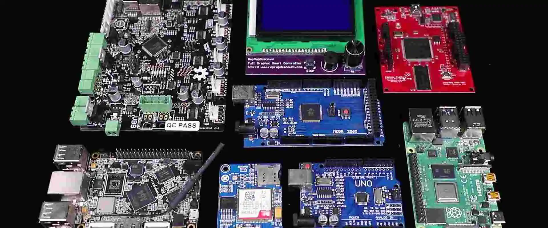
For the majority of electronic equipment, including computers and televisions, a PCB or a Circuit board is a necessary component. This post will explain the fundamental structure and layout. As well as the assembly of a PCB and provide some pointers for building your own. Let’s get going!
You might want to check over some essential electrical principles. For instance, the fundamental circuits, electricity, voltage, connection fundamentals, or solder 101, on this World Electronics before we start.
Printed wiring chips and printed wiring boards are other names for PCBs. These labels are a throwback to the point-to-point cable wiring. When the insulator on the cables started to deteriorate and crack, there were regular short circuits and failures at wire connections.
The invention of wire wrapping has been advantageous for the more current boards. This method wraps a small gauge cable around each connecting point’s post. This actually results in a safe, sturdy, and yet conveniently changeable connection. Furthermore, a switch away from heavy vacuum tubes or retransmits to more compressed and reliable silicon and ICs resulted in a reduction in both the cost and size of components. A rise in demand for lightweight consumer electronics prompted developers to create increasingly more compact products to sell. Go to the PCB.
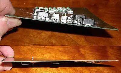
The “B” in the PCB refers to “board.” The stiff board comprises a network of wires and pads interconnecting. The purpose of the PCB is to make it possible to transport power and communications between actual physical objects. The use of solder aids this whole procedure. Solder is a metal (and powerful mechanical adhesive) that carries electrical links from the PCB surface to the components.
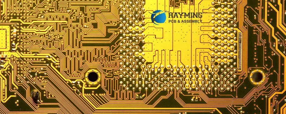
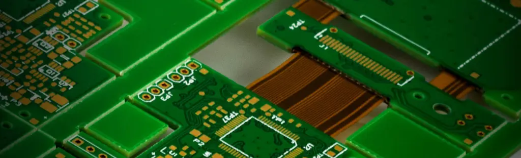
PCBs comprise various layers of different materials layered into one single object. Let’s split one right now, starting in the middle and moving outward from the surface.
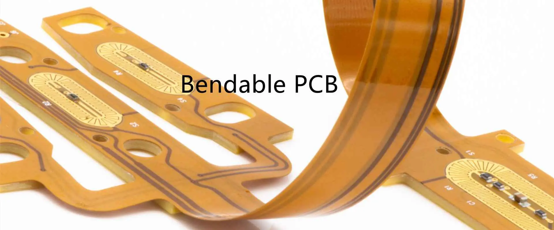
The base or substrate of the Circuit board is where it all begins. The most popular substrate comprises FR4 and Fiberglass. This serves as the PCB’s support structure and lends it its thickness, heaviness, and stiffness. A more flexible type of PCB usually uses a high-temperature polymer like Kapton as a substrate.
PCBs come in a variety of forms and have been in use for many years. Circuits were connected on chasses, which were typically made of a metal structure and a wooden bottom before Circuit boards were invented. An Australian technician created a PCB as a component of the radio device in the 1930s, revolutionizing the field. Thankfully, since systems had to be powerable more effectively and everything had to get smaller. PCBs became more important not just in but of themselves. Moreover, owing to the Net, more linked to the rest of the world.
As a result, there have been breakthroughs in the construction of improved and compact PCBs. Furthermore, greater communication with more products that were previously out of reach, like wearable technology, smartphone apps, and a lot more.
How Does A Electrical PCB Work?
Whenever it concerns its structure, PCBs appear to be really straightforward. However, when it concerns the variety of things, they enable us to do with all of the modern marvels. No matter how basic a device may be, a Circuit board of some kind requires direct energy to pull into the gadget to serve its function. Really, it’s that simple.
Imagine being able to do little miracles. Miracles that were previously impossible with just some resin layers and a few solder channels enable electricity to flow through the various components of a PCB. PCBs support the mechanical aspects of the gadget in addition to channeling power.
This is due to the fact that PCBs direct electrical signals where they should go. Also, they offer a solid foundation for the components to all cling to. A brief glance at a PC and its internal components offers a great view.
Given all this assistance from a Circuit Board, it is easy to understand why PCBs are an item of equipment’s “brains.” Simply said, an electronic device wouldn’t function without any PCB.
Electrical PCB Like Never Before
In addition, PCBs appear to be quite straightforward. Their production involves despite the simplicity of their layout. It starts with a creator and includes the development of electronic layout automation (EDA) programs as well as production, assembling, and inspection.
This is the moment that a skilled circuit designer may truly be priceless. They are able to design a Circuit board that meets all of your unique technological requirements. Also, they’ll make sure you get the resources you require to succeed in your industry and prevent your PCBs from turning into your product’s weakest link. A very well PCB will make it simple to diagnose issues with your apparatus.
As a file containing the layout produces, the production starts right away. The real physical properties of the Circuit board identify and optimized throughout this procedure to produce a device with the fewest possible issues and the greatest possible advantages. Every output that produces needs a careful examination during this procedure to ensure that it performs well.
There is virtually no chance a PCB component will not go through testing with the test methods now available. This will guarantee that the PCB, which thus powers the product, won’t fail later.
MVI used to be adequate for identifying possible problems in electrical circuits, for instance, short circuits. Also, faulty solder connections, interrupted traces, a reversed component polarity, and lost components. Unfortunately, there were issues with the MVI approach, which was to errors by people while they carried out tedious and repeated tasks. This leads to cases where faults were either not discovered or were discovered at a late point in the design. This approach makes it prohibitively expensive to make changes to the circuitry.
The process of visual examination was then by utilizing the AOI method. Nowadays, AOI is a well-established inspection technique that is accessible on a number of pick-and-place equipment and is frequently utilized during welding post-flow and pre-flow. The limits of AOI are no more capable of recognizing the welds and connections concealed inside the package. This has been brought to light by the expanding usage of BGA packages and SMD components. Hence, the AXI, the automatic approach, was created, which is focused on the utilization of X-rays, effectively examining multi-layer Circuit boards with a higher component density in addition to observing the package. Following the inspection step, an appropriate test on the fully built circuit will be done on the Board.
Objective Of Electrical PCB Testing
Each component of a PCB impacts how well the electrical circuit functions as a whole. The following tests must include in the bare minimum set that must be run:
Mechanical resistance,
weld quality,
Mechanical resistance;
Cleanliness which includes humidity, weather resistance, and corrosion;
testing the laminate’s resilience to peeling using force or heat;
testing the tensile strength of copper plating and evaluating the elongation that results;
environmental testing, particularly for PCBs that function in humid settings;
component polarity, location, orientation, and alignment.
· AOI
As an inspection technique, AOI may identify PCB flaws or problems at an early stage of development. AOI refers to a visual inspection technique that makes use of cameras to take pictures of the PCB from various angles and under various lighting conditions. Moreover, this method has OCR technology that can decipher the serigraphs only on Board. The obtained photos were then, therefore, compared with the desired outcome of the golden board. This technique may apply at many phases of development and has the benefit of detecting various sorts of flaws. The key drawback is that it restricts the line-of-sight access, making it impossible to inspect connections covered by some packages or BGA.
· AXI
SMT technology’s great density and the difficulty in seeing connections in CSP packaging and BGA necessitated more precise inspection techniques, such as those that relied on X-ray technology. Welds are easily distinguishable in radiographic pictures. It uses material whose relative atomic mass is greater. Other electronic components on the PCB.
The primary benefit of an AXI approach is the fact that it finds every weld and connection, even those links with packaging. Moreover, solder junctions may examine, which further indicates any potential bubbles. There is also a good likelihood of finding any replicas of exclusive electrical components. AXI, however, is a somewhat pricey method. Its investment can only make sense for highly dense Boards and parts with CSP packaging or BGA.
· In-Circuit Test
This examination, carried out following the assembly phase, confirms the proper operation and positioning of each electrical component upon the PCB. The test thoroughly checks the short circuits, resistance, open circuits, capacitance, and other factors. This uses a flying sensor. This comprises a variety of sensors and drivers that move freely over the board to carry out the measurements that need for the test. By applying the very same test method to PCBs with varied layouts, the software that controls the probe may be changed. As an alternative, a trial fixture comprising a platform of nails for the particular DUT might be useful.
Each “nail” acts as a genuine sensor and is capable of electrically connecting a particular area of a DUT to a testing apparatus. The bed-of-nails approach is costly and offers limitations in flexibility as each board owns bed-of-nails. Moreover, during the pin spacing restriction, it also exhibits certain challenges when testing panels with high-density components. The ICT method offers the benefit of being able to identify a number of flaws in both the connections and individual components without having to power the board. Because of the high cost and complexity of the control and bed-of-nails software, it is not possible to test the connections. Thus, it is a major drawback in both digital and analog systems with several cards.
· Functional Test
The final phase of the examination and verification procedure is the functional test. As its name suggests, its purpose is to test a circuit’s functionality by simulating the electrical impulses capable of activating it and observing the results. The interfaces connect, energize, and electrically activate the board. A software program analyzes the measurements taken at appropriate locations on the Board and confirms that they match the design requirements. The functional test offers the benefit that it can identify possible circuit abnormalities that only appear during the activation of the board. In addition, it can evaluate the power consumption at certain circuit locations. The expense and difficulty of a test system are the drawbacks. In reality, it calls for extremely complex but not particularly adaptable machinery.
Since it’s not feasible to access all of the circuit’s nodes, the boundary-scan approach to examine the connections among components of the board is frequently useful in testing integrated circuits (ICs). The input (TDI) and output (TDO) data pins of the “cells,” which are useful to replace the mechanical probes, are with appropriate shift registers which multiplex circuitry. A Test Clock or TCK signal times the boundary scan circuitry, and a TMS signal activates the test. Hence, the I/Os is without the need for physical test terminals on the circuit using the straightforward 4-wire serial port.
The manufacturers’ Boundary Scan Descriptive Language or BSDL files give details on the boundary-scan parts. The benefit of the boundary scanning approach is that it may be useful for a variety of tasks. These tasks include system-level testing, CPU emulation, flash memory, and RAM testing. The exam can also be performed on the actual playing field. While its principal drawback is it doesn’t provide a comprehensive test. And that only certain components that enable this kind of interface are covered.
Conclusion
Whatever approach is useful, PCB testing is a crucial phase in the electrical design process. Since it may save a great deal of cash and time by spotting any flaws in the board before it is put into final production, in general, all potential flaws may be found using a mix of the aforementioned inspection and testing techniques, with prices varying according to the use and complication of the board being tested.
Electronic circuits use a common type of electrical component which refer as Resistors. Resistors are incredibly significant and well-liked electrical components, just like capacitors. In essence, resistors are used to control the electron flow. The amount of current flowing through the circuit can change. This guide is beneficial to you if you don’t know much about resistors. You will discover more concerning these resistors in this post.
What Is a Resistor?
The majority of electric circuits commonly contain a resistor. An electrical resistor is indeed a passive part that prevents or hinders the passage of charges. Resistance is the ability of a resistor to restrict the flow of electricity through a circuit or a component. Each electrical circuit or component possesses a particular resistance, although some might have insignificant levels that have no impact on the circuit’s current flow. Despite what might seem contradictory, resistors are crucial parts of electrical systems and circuits because of their capacity to restrict the passage of current. This property has several uses.
The equivalent of a resistor would be a little rock or another impediment within a water pipe. So when a pipe or hose attaches to a valve, and a little obstruction comes, less water flows through the pipe. A stream’s tiny plants, boulders, and logs may all be comparable as resistors. These items prevent the stream’s water from flowing continuously.
In the last example, make a voltage regulator by connecting two resistors in series.
If you need variable resistance, a potentiometer can be used in place of an electrical resistor.
Working Principle of Resistor
A resistor collects electrical energy while restricting current flow and lowering voltage, which it then must release as heat. The heat transfer in the majority of contemporary electronic circuits is generally less than 1µW.
Ohm’s law says the following if R represents a resistance measured in ohms, I represents the current flow in the resistor measured in amperes, & V represents a voltage drop due to the resistor:
V=I/R
Another way of expressing that a 1-ohm resistor will admit a 1 amp current flow when there is a 1-volt voltage differential between its ends.
In a Direct Current circuit, if W represents the resistance’s power output in watts:
W=V*I
We may represent watts in measures of resistance and current by substituting them with the law of Ohm:
W=I2/R
Watts is also equivalent to resistance and voltage:
W=V2*R
In circumstances where you are unsure about the current or voltage drop, these alternatives may be helpful.
When employing alternating current, there are roughly the same relationships. However, the voltage becomes a more complicated function of the resistance.
Resistors are useful to reduce the voltage passing across a circuit. It is a rather straightforward gadget. The middle of a resistor constructs with a substance, such as carbon, that only partially conducts electricity. The resistor’s primary function is to lower the current’s voltage. The current voltage decreases when it reaches the resistor’s portion, which possesses poor conductance.
· Carbon Resistor
The most typical kind of resistor is a carbon one. This creates when encircling a ceramic material core with carbon tracks. A machine winds the carbon tracks around the core of ceramic, or a laser engraves the track inside the core. After that, two copper leads are in the resistor’s ends so that the track’s ends touch the leads. Then, the resistor core seals with paint.
· Metal Film Resistor
The construction of a metal sheet/film resistor is fairly similar. This resistor’s ceramic core was useful in its construction. Like all resistor components, this component produces using machines. The track of metal film/sheet resistors comprises metallic oxide substances. Similarly to carbon, this exhibits semiconductive characteristics. Once more, a pressing machine is useful to put copper leads into the resistor’s ends. As a final step, these resistors go through painting.
· Processes
Resistors are almost always produced by machines. Machines are useful to press and form ceramic cores. Separate cores are designed to suit various resistor sizes. The resistor substance is then “wire coiled” all around the cores using a different machine. The ends of lead are then placed over the core, which includes the metal coil end and a cap at the end that resembles a cap of a bottle. The cores have a baked finish or standard paint.
· Resistance Values
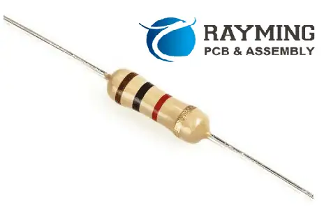
Adding the total resistance to the component is the last step in creating a resistor. To achieve this, draw lines along the resistor’s painted core. Each line is a unique numerical value that is related to Ohms. Black, for instance, is equal to 0, brown to 1, red to 2, and orange to 3. Simple numbers appear on the initial two lines, and the multiplier appears on the third. As a result, a resistor having three bands—brown, red, and orange—would have a resistance of 12,000Ω. As a result, the resistor has a 12,000Ω resistance value.
There are lots of resistor value in the market, Here is top 15 resistor value list that Most people are searching by google :
100 ohm resistor
220 ohm resistor
10k ohm resistor
1k ohm resistor
10 ohm resistor
470 ohm resistor
100k resistor
330 ohm resistor
120 ohm resistor
1 ohm resistor
2.2 k ohm resistor
4.7 k resistor
2 ohm resistor
150 ohm resistor
100k ohm resistor
· Accuracy and Tolerance
Applying the resistor’s accuracy rating is the following step. This is the resistor’s accuracy or tolerance level. Carbon resistors are less precise than metal-oxidized resistors. They are identified with a greater tolerance color due to a greater tolerance rating. A gold band, for instance, is accurate to within 5%. 5 to 10 % accuracy is indicated by silver bands.
Resistors come in a variety of shapes, sizes, and materials. Following, we will go through each potential type of resistor in-depth, along with its advantages and disadvantages.
Resistors come in two different categories.
Linear Resistors
Non-Linear Resistors
Linear Resistors
Linear resistors are those whose values fluctuate in response to temperature and voltage. In other terms, a resistor is a linear resistor if the value of the current is precisely proportional to a given voltage.
There are usually two kinds of resistors with linear characteristics.
Fixed Resistors
Variable Resistors
Fixed Resistors
A fixed or solid resistor is indeed a resistor that possesses a fixed value and whose value cannot be changed.
The types of fixed resistors are
Carbon Composition Resistor
Wire Wound Resistor
Thin-Film or sheet Resistor
Thick-film or Sheet Resistor
Carbon Composition Resistors
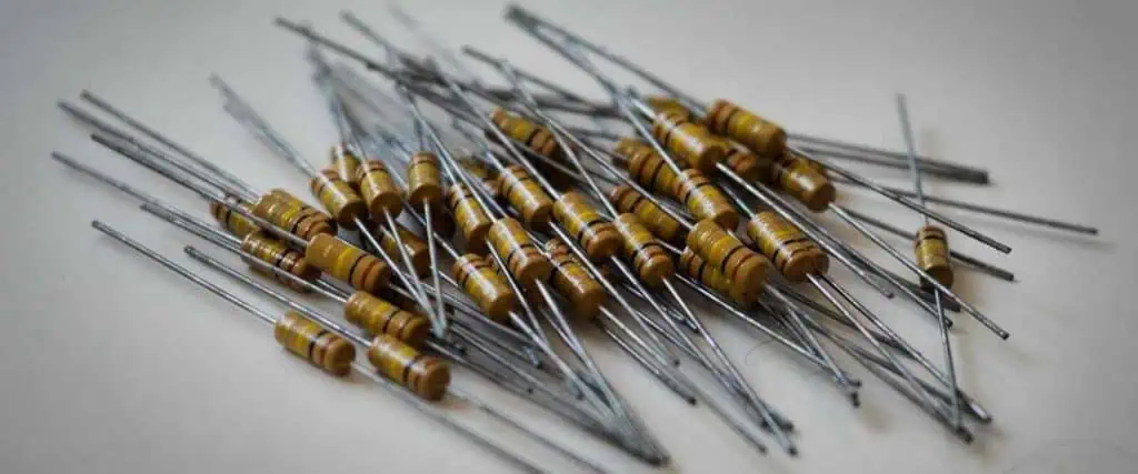
A common solid resistor is composed of a blend of insulating filler, resin binder, and powdered or granulated graphite or carbon. The real resistor’s resistance is determined by the insulating material ratio. The insulator powder or binder is shaped like a rod, and each rod’s end has two metal covers.
The resistor has two conductive wires on each end for quick soldering connections in the PCB. The rods have a plastic layer over them that is printed with various color codes that indicate the resistance level. They come in resistances ranging from 1Ω-25MΩ and with power ratings ranging from 1/4W to 5W.
Characteristics Of Fixed Resistors
They often take up less room because they are compact and extremely affordable. They come in a variety of power and ohmic levels and are trustworthy. Moreover, a solid resistor can handle the additional voltage.
Moreover, due to being less stable, they possess an extremely high TC. In comparison to other kinds of resistors, they also create a little noise.
Wire Wound Resistors
By wrapping a resistive cable around an insulating rod or core, wire-wrapped resistors are created. The insulation core is often constructed of porcelain, press adhesive paper, Bakelite, and ceramic clay. At the same time, the resistance cable is typically made of tungsten, nickel, nickel-chromium base, and manganin.
The expensive manganin wire-wrapped resistors are with delicate test apparatus like the Wheatstone bridge. They come in power ratings ranging from 2W to at least 100W. These resistors have ohmic values ranging from 1Ω to 200kΩ or even more and may be useful securely at approximately 350 °C.
Moreover, the wire-wound resistors have a rating of power of 500W. And the current value of resistance is between 0.1Ω to 100kΩ.
Advantages & Disadvantages Of Wire Wound Resistors
When compared to carbon substance resistors, wire-wrapped resistors are quieter. They function admirably in circumstances of overburden. They are dependable and adaptable, and their frequency range includes both DC and audio. The expense and incompatibility of wire-wrapped resistors prevent their usage in a high-frequency device.
Application Of Wire Wound Resistors
When high sensitivity, precise measurement, and proportional current regulation are required, such as when using a shunt including an ampere meter, wire-wrapped resistors are utilized. Moreover, wire-wrapped resistors are frequently employed in high-rated power equipment and devices, as well as in testing and measurement tools, industrial equipment, and control tools.
Thin Film Resistors
In essence, most thin film or layer resistors are constructed using a resistive substance and a high grid rod of ceramic. A durable ceramic substance or insulating glass plate, rod, or tube with a thin coating of conducting material layered over it. There are also two further varieties of thin film coating resistors.
Carbon Film Resistors
The substrate, which is an insulating core or rod constructed of high-quality ceramic, comprises a carbon-film resistor. All around the rod, just a really thin resisting carbon film or layer was applied. These resistors have a wide working range, less noise, and are more stable than pure carbon resistors, which makes them popular in electrical circuits.
Metal Film Resistors
The construction of a metallic film resistor is similar to that of a carbon-film resistor. The key distinction is the use of metal, or a combination of nickel-chromium, metal oxides, or a combination of glass and metals known as metal glaze, in place of carbon. Metal-film resistors are incredibly small, inexpensive, and functionally dependable. They are utilized in applications where consistency and low distortion level are crucial because of their very low TC (2 ppm/°C).
Thick Film Resistors
A Thick-films resistor is made using the same process as a thin film resistor, with the exception that they have a very thick film surrounding the resistive substance rather than a thin one. It is known as thicker film resistors for this reason. Two other varieties of thick-films resistors exist.
Metal-Oxide Resistor
Cermet Film Resistor
Fusible Resistor
(i) Metal Oxide Resistors
A Metal-Oxides Resistor is easily made by oxidizing Tin Chloride’s thick layer over a heated substrate or glass rod. These resistors come in a large variety of resistance and exhibit excellent temperature stability. Moreover, large voltages may be employed, and there is very little operational noise.
(ii) Cermet Oxide Resistors
The interior portion of the oxidized ceramic resistors comprises ceramic insulating materials. The resistor is then covered with a layer or film made of metal alloy or carbon. It is then finally fixed in a Cermet or ceramic metal. For simple placement on PCB, they are designed in rectangular or square shapes with pins and leads located beneath the resistors. Since their value does not fluctuate with temperature, they offer reliable functioning in high temperatures.
(iii) Fusible Resistors
These resistors are equivalent to wire-wind resistors. This is a fused resistor, which means it opens or breaks the circuit when the power rating of the circuit exceeds the stated amount. It is termed a “fusible resistor” for this reason. Fusible restores serve two purposes, i.e., they restrict current while also serving as fuses.
They are commonly utilized in pricey electronic circuits such as amplifiers, TV sets, and others. Fusible resistors typically have an ohmic value that is below 10Ω.
As per the name, those resistors whose values may be adjusted manually using the right technique or using a knob, dial, or screw. These resistors possess a movable arm linked to the shaft, and by moving the arm, the resistance value may be adjusted. They are employed in the receiver of the radio for controlling tone and volume resistance.
Variable resistors’ types are described below.
Potentiometer
Rheostat
Trimmer
· Potentiometer
A device with three terminals called a potentiometer is useful for regulating the circuit’s voltage level. The resistance between the first two external terminals is fixed, whereas the 3rd terminal is coupled with a Wiper that is changeable. The rotation of the wiper, which is attached to the controlling shaft, will alter the resistance value.
Such resistors are known as variable resistors and allow potentiometers to serve as voltage dividers. They come in sizes of at least 10MΩ.
· Rheostat
Rheostat is a device with at least 2 or 3 terminals. It usually operates manually to restrict current. Tapped resistors and variable wire-wrapped resistors are other names for rheostats.
The Nichrome resistance is wire wound all around the ceramic core, which is then put inside a protective cover to create rheostats. The resistor component is encircled by a band of metal. It is useful as a rheostat or potentiometer.
There are variable wire-wrapped resistors in the 1-150 Ω range. These resistors have power ratings ranging from 3-200W. Rheostats between 5 -50W in voltage level are the most popular.
Difference Between a Potentiometer & a Rheostat
The differences between a rheostat and a potentiometer are minimal. Both resistors are movable. The primary distinction is how the circuit is useful, or more specifically, for what reason do we employ the variable resistor?
For instance, Rheostats are useful when a circuit is connected between the terminals of a resistor element, where one end represents the resistor’s main end while the other represents wiper or sliding contact.
On the contrary, if we follow the same procedure as described above to regulate the voltage level, the same variable resistor turns out as a potentiometer.
· Trimmers
Trimmers are extra screws that are useful with variable resistors or potentiometers for greater performance. A little screwdriver may be useful to adjust the screw’s rotational position in order to vary the resistance value.
They range from 50 Ω through 5MΩ and comprise carbon film, carbon composition, wire materials, and cermet. Trimmer potentiometers have a rated power of 1/3-3/4 W.
Non-Linear Resistor
Non-linear resistors refer to those kinds of resistors which fluctuate the electric current in response to variations in a given temperature or voltage. Besides, non-linear resistors come in a variety of forms, but the ones that are most frequently used are listed below.
· Thermistor
A variable resistor type that can detect temperature changes is the thermostat. Simply put, it’s a two-terminal gadget that’s extremely temperature-sensitive. A thermistor’s resistance is inversely correlated with its temperature.
· Varistor Resistor
A varistor, a semiconductor-based non-linear resistor, means that the current flowing through it does not depend linearly on the given voltage through it. The most popular varistor resistors are called metal-oxide varistors or MOVs.
· Photo Resistor Or LDR
A light-dependant variable resistor is known as a photoresistor, LDR, Light-Dependent Resistor, or photoconductive unit. When the intensity of the incoming light increases, the resistance of the photoresistor lowers.
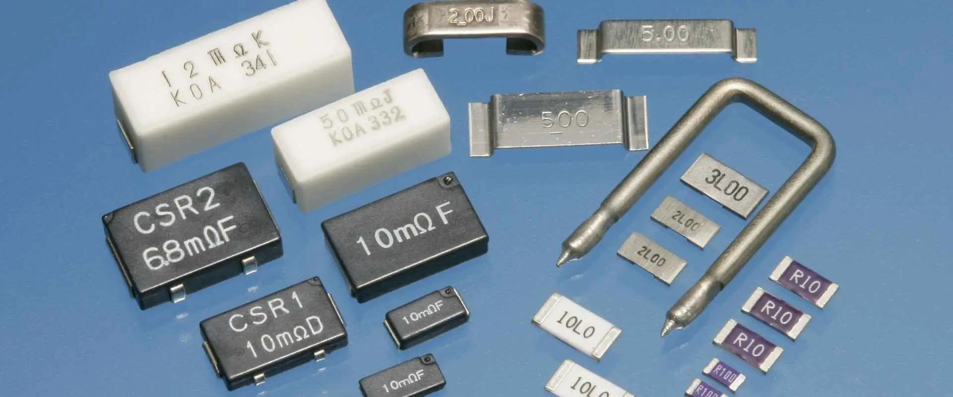
· Surface Mount Resistors
SMD resistors, often known as surface-mounted resistors, have a rectangular form. Electronic parts designed for Surface Mount Technologies or SMT are known as SMDs.
Manufacturing a circuit part with only one characteristic, like pure resistance, inductance, or capacitance, is almost difficult. For instance, a resistor lacks resistance just but rather an affiliated capacitance and inductance. An inductor, moreover, its inductance does have, in turn, capacitance and resistance, as well as a capacitor does have resistance adding to capacitance.
You will be aware of the components useful for resistors.
A circuit element’s impurities lead to the production of residues, which are surplus amounts. Yet, a certain number is designed to dominate. This includes resistor resistance, inductor inductance, or capacitor capacitance to reduce the influence of residues and enable the design of clean circuit components within a given range of precision. This piece helped many people who questioned what materials are useful to make conventional resistors. The following provides the response to the question, “Why and What substance are typical resistance coils constructed of?”
In measurement and instrumentation activities, resistive networks and resistors are frequently utilized for resistors intended for accurate work, stability, or constancy over time, a low TCR, a low electromotive force with copper, and high resistivity. Also, resistance to corrosion, oxidation, and moisture, production simplicity, and affordability are the most important characteristics of the substance’s usefulness.
Yet no material contains all of the aforementioned characteristics; thus, only the substance that is most appropriate for the task at hand is chosen.
The components listed below are useful for creating a standard resistor:
· Manganin
It is a copper, nickel, and manganese alloy that is utilized as a resistance substance in precise resistors and equipment for measuring resistance. The nominal structure of this material is copper 84%, manganese 12%, and nickel 4%. It possesses a thermal Electromotive force of 2-3 V/°C and a resistance of 0.45-0.50*10 (exponential -6) ohm, which is roughly 25 times greater than copper. When heat is properly treated, it provides a consistent resistance value throughout time and exhibits no signs of aging.
The primary characteristic of manganin is its ability to practically have a 0 coefficient of thermal resistance at temperatures close to ambient. As an example, let’s use 0.004 %/°C at 20 °C.
· Constantan
This is a group of copper and nickel alloys having a nickel content of 40-60% and a little bit of manganese for enhancing their mechanical qualities. These alloys all have comparable electrical characteristics. To serve as thermocouple substances, they are offered for sale as constantan and under numerous trade names. They have 40 V per degree Celsius thermoelectric Electromotive forces against copper. Yet, aside from their significant thermoelectric Electromotive forces, these alloys’ electrical characteristics are strikingly comparable with that of manganin.
At normal temperatures, constantan has around 25 times the resistivity of copper, which is highly corrosion-resistant, cheap, and simple to deal with. Soft soldering this to copper is simple. When its high emfs versus copper does not constitute a drawback, it finds considerable employment. For instance, resistors made for a.c. Operations employ this material. It may also be useful in voltmeter multipliers and 1000 ohms resistors and higher if the thermal em-force produced at the copper constantan interface is negligibly little in comparison to the electromagnetic force being monitored.
· Nickel Chromium Alloys
Compared to constantan and manganin, these alloys possess a slightly greater coefficient of thermal resistance. One illustration of this group of alloys is nichrome. Precision resistances cannot be made with these alloys. Nichrome resists corrosion also at extremely high temperatures as well as possessing high resistivity almost 50 times greater than copper. It is frequently employed in the more challenging resistors type, where a tiny size is crucial or high working temperatures apply. Certain alloys are challenging to solder, though.
· Gold Chromium
It is a recently developed alloy that seems quite promising for various uses. It contains slightly more than 2% chromium. At room temp, this alloy contains a resistivity that is around 20 times greater than coppers. By baking alloy at relatively low temperatures, its temperature coefficient may be reduced to an exceedingly minimal value. With copper, it possesses a thermoelectric Electromotive force of 8 or 7 V per °C. Gold chromium alloy is useful for various applications due to its exceptionally low-temperature coefficient, particularly for thermal-resistant criteria.
· Spools For Resistor Coils
In contrast to older wooden spools, metal spools or formers are now often utilized for high durable d.c. Resistors. The benefits of using metal spools include the following;
Unlike hardwood formers, they don’t really collect air moisture. As a result, they don’t even fluctuate in size according to humidity or temperature. As a result, the resistance wire does not experience any fluctuating stresses that may otherwise modify the value of its resistance.
The resistance wire’s current flow generates heat, which is easily dissipated by the metallic spools. This happens when the resistance wire comes in contact with the metal spool. The heat transfers to the metal spool, where it is then released to the environment by radiation and convection. As the spool’s outer surface is already subjected to the atmosphere, its whole surface, including its inside and outside. This effectively dissipates heat, preventing hot spots from developing inside the resistance wire.
Most metallic spools are constructed of brass. This happens because there isn’t much of a difference in expansion between the spool and coil. Since brass does have a thermal expansion coefficient that is almost equivalent to the substances used in resistance coils. As a result, temperature fluctuations do not cause any noticeable alterations in resistance coils.
Due to the loss of eddy current, they induce, using metallic spools in a.c. Applications are not only undesirable but also completely out of the question. The most common material for manufacturing a.c. The resistors’ spools are ceramic. Ceramic spools’ weak heat conductivity and substantially lower thermal resistance of linear thermal expansion than resistance wire are drawbacks of using them in high-precision resistors. As a result of differential expansion brought on by temperature fluctuations, strains are created in the coil windings.
· Resistance Wires
The resistance wire is often wrapped with cotton and silk or double silk. Before applying these coats, the wire is enameled.
Even though this necessitates using smaller cables than multilayered coils, high-standard resistors are coiled with just one coat of wire. Benefits of single-layered coil include:
Single-layer wires provide more effective heat dissipation. On the contrary, the center layers of multi-layer wires are hotter.
Coils with a single layer are more resilient. Multi-layer materials are less likely to adapt to changes in ambient humidity.
Multi-layer coils typically exhibit a decrease in resistance stability over time.
Resistors are commonly useful in everyday electrical devices to control the amount of current that flows through them. It ensures that the devices work correctly. Nearly all electrical components encountered a resistor in them. Let’s take a look at some real-life instances of resistors.
1. Street Lighting
Streetlights turn on by themselves at night and turn off during the day because they have photoresistors. Photoresistors are sensors that can detect the level of light around them. When it’s dark, the resistance of the photoresistors changes, and this tells the circuit in the street lights to turn on. When it’s light outside, the resistance varies again, and the course turns off the lights. You can place photoresistors so they don’t confuse by shadows or car headlights. You can also use these sensors in cameras and burglar alarms.
2. Laptop and Mobile Chargers
Resistors are useful in laptops & mobile chargers to manage the flow of electricity and prevent overheating. The charger has different current readings, such as 2A, 1A, 500mA, or 700mA, which show how much electricity can pass through and how fast it will charge the device.
3. Temperature Control
By changing the resistance in a circuit, we can change its temperature. Joule’s Heating law explains this. It says the amount of heat a board produces depends on the current, resistance, and time. If we increase any of these factors, the heat will also increase. So, we can control the temperature in a circuit by adjusting the current, time & resistance values.
4. Fan Speed Controller
We can adjust the ceiling fan’s speed by turning a knob on the PCB. The knob has a connection to a particular resistor known as a potentiometer. So when we turn the knob, it changes the resistance and the amount of electricity flowing through it. It lets us control the fan speed utilizing the potentiometer.
5. Measuring Electrical Current
To measure current in a circuit, we can connect resistors of known resistance in a series. We use a particular resistor called a shunt resistor for this. Shunt resistors have high power/energy ratings & minimal resistance values. By measuring the voltage drop across the shunt resistor, we can calculate the current in a printed circuit board. One can do it by using Ohm’s law with voltage and current values.
6. Temperature Sensor
These sensors determine/calculate the hotness or coldness of non-living and living things. So thermistors are often useful in these sensors. You can use thermistors because they are sensitive to small changes in temperature. When the temperature changes, the impedance of the thermistor changes too. If the temperature is low, the resistance is low, and if the temperature is high, the resistance is also high. Temperature sensors measure this resistance and convert it into signals that provide readable temperature units like Fahrenheit and Celsius.
7. In-Circuit Functioning
In devices where we need to control the flow of electric current, like changing the pitch of a musical tone, adjusting the amplifier’s volume, or holding the speed of electric motors, we use variable resistors. These resistors let us change the current amount flowing through the device by rotating or sliding a knob that adjusts the resistance.
8. Heating Appliances and Lighting
Heating appliances such as heaters, kettles, electric ovens, and toasters have resistors. The resistors change the current into temperature/heat, which warms up the devices. The light bulb filaments utilized in these appliances also act like a resistor. It decreases the current and warms the filament wire until it produces light and heat.
9. LEDs & Transistors Protection
LEDs and Transistors are easily affectable by electric current. Too much current can damage their sensitive parts, while too little wind can affect their performance. To prevent this, you can link a fixed-value resistor in a series with the LED. These resistors only allow a specific current range to go through the device. These resistors are ballast resistors, and they protect LEDs from damage by limiting the current flow.
10. Timing Circuits
The resistors are useful in equipment that requires timing circuits, such as electronic sirens and light flashers. These timing circuit boards use resistors and capacitors or inductors, which store the energy from the voltage source. Capacitors slow down voltage change, while inductors slow down the electric current change. The time taken by the inductor and capacitor to charge depends on the resistance utilized in that board. If the resistance is high, it takes a long time to charge up, and if the resistance is low, it charges up quickly.
11. Lighting Circuits in Houses
In-home lighting systems and parallel resistive circuits are better than series circuits. If we link resistors/capacitors in the line, switching off a light bulb would switch off every bulb in the house. Also, in a series circuit, the current across all the loads is not the same. With more loads, the current per load decreases, and the load farthest from a source gets a nominal voltage. Thus, we use parallel resistive circuits where the voltage(current) across every load becomes similar, and turning off one bulb won’t switch off all bulbs because each bulb has its current/voltage source.
12. Blower Motor Resistor
It is a device that runs a fan to keep the air moving in a car’s ventilation system. To control the speed of the fan, use a blower resistor. The resistor is in series with the blower fan to regulate the electric current going through a motor. It usually has several resistors, and you can use it to adjust the fan’s speed by changing the resistance. You can use different designs to construct blower resistors, such as wound resistors placed in series or integrated circuits mounted on PCBs.
A resistor controls the flow of electrical current in an electronic circuit. It can also provide a specific voltage for energized equipment, like a transistor.
What are the four main types of resistors?
Types of Resistors
Fixed Resistors.
Linear Resistors.
Non-Linear Resistors.
Variable Resistor.
What are a resistor and unit?
Resistors are components that slow down the electricity flow in a circuit. Commonly you can find it in electronic circuits and electrical systems. You can calculate resistance in units called ohms.
Why are resistors essential?
Resistors create a voltage drop in electrical circuits, which helps ensure that components receive the correct amount of voltage. It can also protect members from sudden voltage spikes. Different elements in a board, such as lights or switches, require specific voltages to function correctly.
What is the resistor’s principle?
The resistor slows down the flow of electricity and reduces voltage by absorbing electrical energy. So in modern electronic circuits, this heat release is usually a tiny amount, less than one watt.
Are resistors AC or DC?
Resistors work in DC and AC circuits, while inductors only function in Direct Current circuits.
What are the two types of linear resistors?
There are two types of linear resistors: variable resistors and fixed resistors.
What are the main types of fixed resistors?
The primary kinds of fixed resistors include thin-film SMD resistors, wound resistors & carbon resistors.
What are the main types of variable resistors?
The primary forms of variable resistors arethermostats, potentiometers & trimmer resistors.
What is the use of resistors in the case circuits with LEDs?
When it comes to LEDs, the consequences of excess voltage can be dire since they are susceptible to changes in current. To prevent this, you can implement resistors to regulate the current that flows through the circuit.
By doing so, not only do they help avoid LEDs and other semiconductors from damage, but they also allow them to function within their optimal current ranges. LEDs are an essential component in various electronic devices, from simple household appliances to complex scientific instruments. Without proper current regulation, these devices would be susceptible to damage or failure. They are underscoring the vital importance of implementing resistors as a means of current control.
Conclusion
While we have discussed several vital parameters one may encounter while designing a board containing resistors, we cannot disregard others.
In most cases, a regular 1 percent metal film resistor with a power rating of 0.125 watts is sufficient for applications. However, certain products require a deeper understanding of a resistor’s specifications to ensure optimal performance. It is especially true for applications like power supply layouts, high-frequency layouts, audio work & products that operate in high ambient temperatures.
To achieve a highly reliable design and potentially prevent a time-consuming redesign, it is essential to meticulously examine the specifications and exercise great caution when selecting the appropriate resistor. By doing so, one can ensure that the resistor suits the application’s demands, thereby maximizing the effectiveness of the overall design.
If you have ever had a professional circuit board made, you were likely presented with a choice between ENIG and HASL surface finishes. These finishes differ in several ways, from their solderability to their cost. Although some manufacturers have a preferred option, you may be curious about the distinctions between these two.
HASL is a surface finish method that entails dipping copper in the pool of melt solder. The excess solder is then removed, and the finish is leveled using a set of compressed hot-air knives before the hardening of the solder. This technique results in a robust coating that shields the copper. It simplifies the assembly process and is widely used as a contact plating strategy due to its numerous advantages.
Although HASL is a great technique, it does have its drawbacks. PCB manufacturers commonly use ENIG as the gold plating strategy due to its numerous advantages over other ways. ENIG produces a much flatter surface, essential for properly adhering to big ball-grid packages. The absence of lead in the manufacturing process of ENIG boards enables a considerably cleaner, safer, and ecologically sustainable production process. Furthermore, eliminating the air knife step reduces the warping of boards. It is particularly when they are thin and enhances their thermal durability to some extent.
As a part of the production process, surface finishing is applied to PCBs to enhance their functionality, durability, and appearance. This process involves treating PCB surfaces using techniques such as coating, electroplating, and polishing.
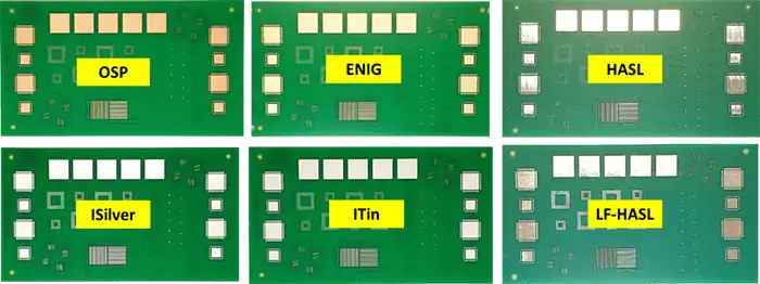
Various surface finishes are commonly used in the manufacturing of PCBs, including:
The Difference Between HASL and HASL Lead-free
HASL (Hot Air Solder Leveling): The method entails submerging the PCB in a pool of liquefied solder and applying warm air to even out and refine the exterior.
ENIG (Electroless Nickel Immersion Gold): In this technique, a fine coating of auto-catalytic nickel is administered onto the surface of the PCB, followed by a delicate layer of immersion gold. This surface treatment is renowned for its robustness and ability to withstand oxidation.
OSP (Organic Solderability Preservatives): The procedure consists of administering a slim coating of the organic compound onto the surface of the printed circuit board to safeguard it from oxidation and enhance its solderability.
Immersion Tin: The process of achieving a smooth surface texture for PCBs entails applying a tin coating that offers excellent protection against corrosion and reduces contact resistance.
ENEPIG: This particular surface finish represents an upgraded variant of ENIG, featuring enhanced resistance against corrosion and outstanding shelf life.
Immersion Silver: Coating the PCBwith a coating of silver, akin to Immersion Tin, is the surface finish technique employed here, which endows the board with commendable resistance against corrosion.
Gold Plating: The surface finish method employed here entails applying a layer of gold coating to the PCB, as the name implies.
When it comes to selecting the ideal surface finish for a particular application, several factors need to be taken into consideration. It includes the kinds of components utilized, the operating environment of the PCB, and the price analysis.
Moreover, solderability, cost-effectiveness, reliability, processability & compliance with lead-free needs are crucial factors that must be evaluated. Two commonly used surface finishes with excellent solderability are ENIG and HASL.
In lead-free appliances, compliance with RoHS and WEEE regulations for surface finish may be necessary for the printed circuit board.
What is HASL?
HASL is widely recognized as the most prevalent surface finishing technique employed in the production of PCB. This method entails submerging the PCB in a pool of melted solder, smoothed by hot air. This procedure is essential in creating an even surface finish on the printed circuit board, as it plays a critical role in ensuring appropriate soldering and stable component installation. The solder pool can consist of a combination of Tin and Lead, typically with a proportion of around 63 percent Tin and 37 percent Lead. However, if the lead-free PCB is desired, the HASL process can be slightly modified to accommodate this change.
Lead-free HASL contains approximately 99.3 % Tin & 0.6 % Copper. Despite being visually and functionally similar to Hot Air Solder Leveling, there are some differences in the production process. For instance, a lead-free Hot Air Solder Leveling alloy has a higher M.P. than lead solder, necessitating adjustments in the soldering process.
Despite its widespread use, HASL has certain drawbacks, including low reliability, high lead content in humidity environments, and the potential for inadequate soldering performance. The surface finish may also be uneven, rendering it unsuitable for high-density components and having poor shock resistance. Furthermore, plated via elements are unsuited for this finish surface.
As mentioned earlier, there are two varieties of HASL surface finishes employed in the fabrication of PCBs: Lead-free Hot Air Solder Leveling & Lead-based Hot Air Solder Leveling.
The Lead-based Hot Air Solder Leveling process is a traditional finishing method for printed circuit boards that involves molten solder containing lead. The resulting surface finish of the lead-based Hot Air Solder Leveling has a shiny and more reflective appearance.
The lead-free Hot Air Solder Leveling process utilizes a tin-copper or tin-silver alloy for its finish, eliminating the use of lead. This alternative approach boasts superior reliability even in extreme temperature & humidity conditions.
Despite its long-standing use, HASL is replaced by more eco-friendly and dependable surface finishes, including Immersion Tin and ENIG.
What is ENIG?
In the manufacturing of printed circuit boards, ENIG serves as a surface finish method that involves electroless plating of a thin nickel layer. Unlike other plating processes, this chemical process doesn’t need external electrical input. The resulting coating offers a smooth foundation for the gold coating to stick to and exhibits remarkable resistance against corrosion. After the nickel layer has been applied through electroless plating, the board is submerged in gold plating for a process known as immersion plating. The immersion plating process deposits a layer of gold onto the nickel surface, which enhances the board’s electrical conductivity & minimizes contact resistance.
ENIG surface finish consists of a dual-layer metal surface comprising a nickel layer and a thin coating of gold. This finishing process is ideal for mounting components such as SMDs. The nickel layer ranges from four to seven um in thickness, while the gold layer ranges from 0.05-0.23 um. So this method conforms to the RoHS standards, making it an eco-friendly choice.
ENIG finish
ENIG is a cost-effective, lead-free solution that offers less contact resistance, corrosion resistance & strong adhesion, making it ideal for surface mount technologies. It boasts consistency and long life, making it a dependable choice.
1. Nickel & Gold, when combined, exhibit favorable resistance against corrosion, rendering them appropriate for electronic applications that endure challenging environmental conditions.
2. Having a layer of Gold atop Nickel results in excellent electrical conductivity & minimal contact resistance, critical for appropriate soldering and ensuring the stability of the components.
3. ENIG is a viable option for mounting devices & components, as it eliminates the need for a solder mask coating and offers a level surface for Surface-mount devices elements.
4. Applying ENP Gold results in a consistent and sleek surface texture on the PCB.
ENIG plating
The reliability of ENIG plating is questionable due to reported dependability problems. Plating often results in non-uniform wetting, separating copper traces from a finish. To ensure optimal performance, it is crucial to regularly replace the reductant. It contains Nickel ions to maintain the appropriate temperature & concentration levels of the coating.
Applications of ENIG
PCB manufacturing utilizes various surface finishes for different applications. Here are some examples.
In printed circuit board manufacturing, surface finishing is essential for safeguarding the copper circuit on a board from oxidation. By coating the base surface of an exterior layer, the surface finish helps to protect the exposed copper circuitry.
The procedure additionally furnishes a surface that can be soldered when assembling electrical components onto the PCB.
Using surface texture in PCB manufacturing offers numerous benefits. Here are some of the advantages.
Ease of soldering: The application of ENIG or HASL as surface finishes results in a sleek surface on a PCB facilitating effective electronic assembly soldering.
Corrosion resistance: Immersion tin surface finishing creates a layer that resists corrosion, safeguarding the PCB from harm, even in severe environments.
Improved electrical performance: Surface finishing with immersion silver/OSP results in enhanced electrical performance of the PCB, accomplished by reducing the surface impedance.
Enhanced appearance: By utilizing gold and other specialized plating techniques during surface finishing, a visually pleasing appearance can be achieved on the PCB.
Low cost: OSP and HASL are the most commonly employed surface finishing methods in PCB manufacturing due to their cost-effectiveness.
Likewise, every surface finish technique has its drawbacks, but some general disadvantages are:
Complicated system: Achieving a smooth surface finish on PCBs is a complicated task that calls for specialized equipment & expertise. As a result, the manufacturing process of PCBs may incur additional expenses and prolonged production time.
Environmental problems: There is a need for various surface finishes to be made more eco-friendly. HASL, in particular, has the potential to emit toxic fumes during coating procedures, posing a threat to both workers & local community.
Product shelf life: Using OSP as a coating for the PCB can result in a restricted shelf life & potential degradation of the board over time.
Compatibility issues: It is important to note that not all surface textures are suitable for every type of PCB material & component. Hence, manufacturers must consider compatibility factors during the manufacturing stages.
Application-specific downsides: The electrical properties of certain surface finishes, including impedance & loss tangent, make them unsuitable for high-frequency applications. Similarly, some surface textures can not be appropriate for heat-intensive applications owing to their thermal properties.
Individuals in the PCB industry likely comprehend the purpose behind copper textures on the surface of PCBs. When left exposed, copper oxidizes and deteriorates, making the PCB unusable. While there are numerous forms of surface finishes available, it’s essential to understand their impact on the connection between the element & PCB.
Surface finishing serves two essential purposes in the PCB industry: protecting the copper circuit and facilitating the soldering process during the assembly of PCB components. To better understand PCB surface finishing, we will compare ENIG plating & HASL finish.
1. Cost Difference Between ENIG vs. HASL
Due to its affordability and sturdy composition, HASL has been a favored option for surface finishes across various applications. This prevalent surface finish is available in many variations. Its application process exposes the printed circuit board to temperatures as high as 265 degrees Celsius. It enables the identification of assembly issues before attaching any components to the board. These attributes make it an attractive choice for cost-conscious users.
In contrast to HASL, ENIG is comparatively more expensive due to the gold plating process and the utilization of multiple-layer boards. However, ENIG boasts impeccable corrosion resistance, rendering it suitable for aluminum wire bonding, high-density technology & advanced solderability. Opting for ENIG may be a wise investment as it offers a superior shelf-life and delivers optimal value for money.
2. ENIG vs. HASL Have Different Operation Steps
The Hot Air Solder Leveling process involves placing copper in the vessel of molten solder. It is followed by the use of hot-air blades to remove any surplus solder and refine the surface texture. Once the solder cools and solidifies, the outcome is a robust and dependable coating that safeguards copper against corrosion. This process is ideal for users seeking a simple assembly process and a durable coating.
In contrast, the Electroless Nickel Immersion Gold process is a gold immersion plating procedure exclusive to printed circuit board manufacturers. The outcome of this process is a smoother surface that facilitates the secure attachment of big BGA packages. Additionally, since ENIG plating doesn’t require a hot-air blade process, its circuit board exhibits superior thermal durability. However, the intricacies of the ENIG plating process may prove to be too challenging for users lacking in-depth knowledge of the production process.
3. ENIG vs. HASL Service Life
While HASL may appeal to those seeking to reduce expenses, manufacturers have recognized that it lacks the necessary durability. Due to the challenging soldering process required when attaching other printed circuit board components, it is unsuitable for minimal shock applications.
ENIG boasts a sturdy and long-lasting metallic coating consisting of nickel, fortified for added durability. To enhance accessibility in storage, a coating of gold is there to safeguard the nickel layer. Despite being pricier than HASL, ENIG offers outstanding electrical performance, a distinguishing feature that confers longer shelf life compared to alternative coating alternatives.
4. Surface Treatment Between ENIG vs. HASL
To succeed with the Hot Air Solder Leveling process, all layers of solder coating must exhibit a uniform, smooth, and bright surface with fewer defects.
However, the HASL method tends to produce coatings with poor smoothness due to its reliance on high temperatures. It may ultimately impact the performance of your PCB.
Additionally, the uneven finish that often results from the HASL process can limit the use of printed circuit boards that contain high-quality pitch components within their design.
ENIG provides a consistently smooth surface finish, attributed to its metallic coating comprising nickel. This coating not only adds a protective obstacle to a copper circuit but also safeguards the surfaces onto which components are soldered. Additionally, a gold layer acts as a protective shield during the storage process for a nickel.
5. Selection of Thin & Thick Plates
With HASL, board thickness can reach up to two hundred miles. However, since the procedure relies on onboard technology, it may cause slower electric conductions in certain cases.
ENIG’s plate is a favorable electrical connector due to its minimum gold thickness of five to fifteen inches, making it easy to solder. Additionally, its exceptional wear resistance allows for reliable rotary switches.
6. Difference Between ENIG vs. HASL Unleaded and Leaded
Different types of HASL are available, classified into two primary groups: lead-based &lead-free. However, most variants contain hazardous substances, including lead & toxic chemicals. It poses a potential risk to designers who work in a place without appropriate protective measures and ventilation. Thereby jeopardizing their health and safety.
ENIG is available in various versions, catering to the needs of both high-end and budget-conscious electricians. However, low-quality Electroless Nickel Immersion Gold variants may have insufficient nickel/gold plating, leading to “black pad” issues. Conversely, high-quality Electroless Nickel Immersion Gold plates use adequate amounts of nickel & gold coating to combat the negative effects of lead & emissions.
7. Differences in Bonding Strength Between ENIG vs. HASL Plating
The Advantages and Disadvantage of HASL Surface Finish
Hand soldering is the most suitable method with HASL, as the joints tend to form quickly. If the soldering material is the same as the material useful in HASL. Then it’s important to have strong adhesion because the materials interact with each other at a very small molecular level. The bonding strength of HASL makes it highly dependable, especially for sleek finish applications.
ENIG boards undergo a uniform coating process using gold and nickel to get the proper bond. A new nickel layer solution is available with better properties that control the stability of the solution and reduce the brittleness of the nickel layer, resulting in better flexibility. Additionally, the new kind of immersion gold solution used in PCB immersion has a neutral PH value. It makes it cost-effective and corrosion-resistant.
8. Solderability & Corrosion Resistance
The HASL finish offers high solderability for a PCB, and its robustness allows for easy soldering and assembly during multi-step processes. However, the Hot Air Solder Leveling process involves submerging the whole printed circuit board. It can result in additional thermal pressure on the board.
With ENIG, the solder joint is between the Nickel layer and the solder. It’s crucial to avoid exceeding this layer to reach the copper. It’s also essential to dissolve the gold completely into the solder joint. The new immersion gold solution used in the process has exceptional oxidation resistance, protecting the copper.
Wrap Up!
It’s essential to compare the difference between ENIG and HASL when searching for a high-quality printed circuit board surface finish. HASL may be the best option for those seeking a low-budget finish.
However, for specific applications such as keypads, lead-free layers, and wire bonding with a through-hole plating solution, ENIG is the optimal choice.
Whether you need HASL/ ENIG surface coating for your PCB, look no further than RayPCB. Our focus isn’t solely on profit; rather, we prioritize ensuring that you receive the best value for your investment. With our tailored solutions, we offer a vast array of technologies to suit your specific needs. Don’t hesitate to contact us today to fulfill all your printed circuit board surface treatment needs.
Printed circuit board etch-back is a technique used to maintain optimal transmitting signals between many layers in PCBs. It is specifically used with PTH procedures, where producers add a copper coating to the interior sides of the via. PTH enhances conductivity by linking the circuits in multilayer printed circuit boards.
Understanding PCB Etch Back Processes
PCB etch-back is a crucial process to maintain optimal routing signals between multiple layers within printed circuit boards. It involves removing the epoxy glue from the edges of the drilled via to allow electroplating and maintain the high link between layers. This process is especially important in high-reliability appliances. It is subject to standards set by an IPC-6013, which dictate that etch-back must expose a minimum of 0.003 mm and 0.08 mm of copper as specified in the Procurement records.
To improve the adhesion via plating, micro-etch procedures are used, which involve submerging the base laminate & drilling PTH into a multilayer printed circuit board. The dielectric debris and excess smears from a plated sidewall are then removeable using a plasma etch in the process known as de-smearing.
Moreover, PCB manufacturers utilize PCB etch-back in conjunction with de-smearing processes. PCB etch-back removes material from a via hole and extends copper layers to improve the electrical conductivity of the printed circuit board. This process allows producers to plate 3 edges of a copper layer & promotes the sustainability of the PCB design.
Two common processes in flexible circuit production, micro-etch & plasma etch, can impact etch-back. To enhance Coating adherence, the laminate substrate is often treated through a micro-scale etching, where a small copper is removed by submerging or spraying the substrate. After laminating the circuit layers together and drilling through holes, a plasma etch is performed to remove any organic resins or debris, also known as desmearing. It ensures the surface of copper in the via hole is lead-free. The plasma etching is carefully controlled to remove a specified amount of dielectric, revealing the copper coatings.
Causes of Epoxy Resin Smears
When the temperature of a drilling process surpasses the glass transition temperature of a substrate, it can melt the dielectric resin and its dispersion on the copper texture of interior layers, causing smears. This melted resin may obstruct the terminals of inner layers, leading to a decrease in the effectiveness of electrical connectivity.
Type of PCB Etch Back Processes
Two primary types of printed circuit board etch-back exist, namely negative & positive, and they yield various appearances & outcomes.
· Negative PCB Etchback
In negative printed circuit board etch-back, the inner copper coatings gradually recede from the walls of the via hole to varying degrees depending on the configuration of the PCB.
Negative etch-back is less aggressive and is more suitable for the production of high-durability & long-term installations.
Polished copper cylinder walls by negative etchbacks, which do not have stress points within the inner plane. But if we use these processes too much, it can cause gaps between layers because of dirt and air bubbles.
· Positive PCB Etchback
On the other hand, positive PCB etch-back results in copper pads sticking out from the intersecting edges of the via hole, which provides a sturdy Tri-terminal connection. This type of etch-back is commonly useful in highly reliable multilayer printed circuit boards, particularly in the aerospace, medical & military fields.
Positive etch-back is also useful to remove smears of dielectric substance aggressively. However, one significant disadvantage of this method is the potential formation of Pth barrels & foil cracks by strain accumulation on a fabric. Despite this drawback, positive etchback is still available.
PCB manufacturers have several options for etch-back techniques, each utilizing different solutions and yielding varied outcomes depending on environmental conditions. These options include chemical and plasma etch technologies.
· Chemical Etch
Chemical etch processes typically use a basic etching solution of potassium permanganate, usually removed via plating. Another option is sulfuric acid, which removes water from the air and has a limited period, changing resin-reducing rates based on purity.
Another chemical etch option is chromic acid. It gives a uniform resin removal rate but comes with water pollution hazards.
· Plasma Etch
Plasma etch-back is an expensive technique useful in PCB manufacturing that offers fast and effective stain removal. The process involves creating volatile radicals that corrode epoxy glue buildup, making gases that producers eliminate at the last step of the procedure. However, plasma etch-back can increase the total price of PCB production due to reduced manufacturing throughput and longer processing time. Additionally, after the plasma etch-back, you still require a chemical desmear procedure to get the glass to etch & remove any fiberglass.
Difference between Chemical & Plasma PCB Etch Back Processes
Etching is the process of removing copper & unprotected areas, leaving the intended board behind. There are two main methods of etching: chemical etching and plasma etching. Although both techniques serve the same purpose, they differ in several ways. The following are some of the differences between chemical etching and plasma etching.
· Efficiency
The most significant difference between chemical etching and plasma etching is their efficiency. Chemical etching, which removes unprotected areas by dissolving them, is effective, however inefficient, similar to digging a ditch. In contrast, plasma etching has set new standards by greatly improving efficiency.
· Etch-back
Another difference between chemical etching and plasma etching is the occurrence of etch-back. During the chemical etching procedure, etch-back or undercutting always occurs, which requires increased trace widths. The thickness of the copper also affects the etching time required to eliminate copper, which is present between the pads. On the other hand, the new procedure of plasma etching eliminates the occurrence of etch-back. Therefore, the occurrence of etch-back is another distinguishing factor between chemical etching and plasma etching.
· Etch factor
Plasma etching is crucial as it reduces imaging errors by utilizing an imaging process that transfers the layer to the substance/material, thereby eliminating an etching factor. But the chemical etching procedure is the traditional method that results in a distorted side of the pad. With chemical etching, there is a certain slope amount for every wire height increase.
Unlike chemical etching, plasma etching does not use a hot chemical solution like a manganate (VII) solution. It is a dry technique that is eco-friendly and has been proven effective in completely removing any leftover epoxy resin from the printed circuit board drilling process.
Compared to permanganate solutions, which rely on wet chemistry & chemicals that lose effectiveness over time, plasma ashing is a cleaner and more consistent process. It does not generate any hazardous liquid chemical waste. Additionally, the equipment needed takes up less area on the fabrication floor. Additionally, the plasma treatment tool is easy to operate and does not require highly-skilled personnel.
Wrap Up!
The terms “de-smearing” and “etch-back” may be used interchangeably by some manufacturers, but these two processes are slightly different. In particular, it is possible to perform de-smearing without requiring resin etchbacks.
De-smearing, or smear removal, removes resin from the via hole wall side to ensure proper interior layer electrical connectivity. Etchback, on the other hand, improves conductivity by extending or etching the copper layers. While some manufacturers may use the terms interchangeably, there are slight differences between the two processes. Etchback is more effective in multilayer printed circuit board configurations, while you cannot use it for PCBs with double sides.
Furthermore, chemical etch-back strategies are generally more cost-effective than plasma methods. Still, they are less efficient & involve caustic chemicals that may pose hazards during handling. On the other hand, plasma cleaning treatments offer greater precision, allowing for better customization and fine-tuning of the drilling process.
PCB manufacturers can opt for plasma processes as a safe & eco-friendly alternative to chemical etch-back methods. Plasma processes produce by-products that discard without gathering hazardous waste. By partnering with a specialized printed circuit board etch-back professional, manufacturers can achieve higher adaptability, optimized repeatability & precision for even the most complex fabrication processes. It leads to more reliable, more sustainable printed circuit boards, reduces waste & improves reliability. Although plasma etching eliminates the need for additional time to rebuild boards, resulting in low cost.
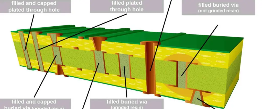
Boards must include via holes in order to establish electrical contacts between traces on different layers. But did you realize that vias might be useful to plug these holes?
Surprisingly, vias plugging refers to the common procedures used by the majority of PCB producers to safeguard PCB vias. What, though, is through plugging exactly? Continue reading to learn more about the limitations of filled holes or vias and the various methods for vias protection or plugging.
What Is PCB Via Plugging?
Manufacturers employ the method known as via plugging to fill holes or vias with solder masks or epoxy. Unlike via tenting, when makers fill the holes instead of covering them, this is the complete opposite.
Plugging in might be viewed as a safety precaution. During assembly or soldering, it stops additional solder substances from pouring into the soldered hole.
In simple words, disconnected vias provide spaces for unwelcome solder paste to flow, resulting in solder junctions. It’s interesting that manufacturers may plug vias with both conductive and non-conductive substances.
Also, the use of non-conductive substances to plug through holes won’t have an impact on how they work. The disadvantage is that they are not strong enough to withstand larger current loads.
On the contrary, vias that have been filled with conductive substances may easily transfer significant current loads between layers. There’s a grab, though. Conductive material-containing vias might have significant CTE.
Hence, there is a good likelihood that the conductive substance will heat up and expand more quickly than the laminate around it. However, such circumstances may lead to cracks between the contact pad and the wall.
When temperature or a significant quantity of current has to be transferred from one portion of a board to the other, conductive-filled vias are typically employed. They are located underneath chips where excessive heat is an issue. Also, there will be a great deal of heat being produced. The metallic quality of the filler will typically conduct heat like a heater in many aspects, from the microchip to another edge of the circuit.
The mismatch in CTE between the surrounding laminate and metallic fille is the fundamental disadvantage of conductive-filled holes or vias. Fractures or Cracks between the holes and pads wall may result from the metal’s fast expansion and heating relative to the laminate around it. Although the fill’s goal is to increase the integrity of the metal pad, plated on holes. Conductive filled holes or vias really aren’t advised for Via or through-hole In Pad process due to this.
· Non-conductive Fill
It’s a frequent fallacy that perhaps a non-conductive filled will allow just a very faint electrical signal to travel through a via if any, electrical signal at all. It is untrue. The only change is that the fill substance is used in place of the empty space in the barrel’s space of the vias. They may still be coated with copper like every other via holes on the circuit. This is often done to stop solder and other impurities from getting into the through. Or for a via-in pad to give structural strength to a metal pad surrounding the exposed hole. A mask-plugged hole or vias is also known as a non-conductive fill.
Plugged Via Shut With Copper
This refers to an early callout that is occasionally found on heritage goods. This was originally intended to be a means to create a copper conductive stuffed via as the copper utilized to print a via sealed will also print across all copper aspects on the circuit. The challenge with this procedure involves the fact that the vias must be very tiny to make this practical. All holes and copper on the surface.
As one copper oz is equal to 1.4 mils, it takes 2.8 oz of plating to cover an eight mil drilling hole. Because the plating is used on both “ends” of the hole barrels, 8mil/2 is equal to 4. 4mil/1.4 is equal to 2.85oz. This really is 2.85 oz more copper than what is currently on the board’s surface. This would increase the overall copper weight of the design to 3.5-4 oz. With this much copper, it is impossible to create intricate trace designs or tight spaces.
The enormous difficulty in coating the hole’s whole barrel equally is another disadvantage. A hole may seem sealed, but the middle may contain trapped air or fluids that will release when subjected to assembling temperatures since the hole barrel tends to plate quicker toward the holes’ bottom and top. We won’t try this kind of fill because there are far more dependable options available.
As previously noted, there are two ways to plug a visa. However, it varies depending on the substance (non-conductive or conductive materials). The non-conductive through plugging is much more common among these two. Now let’s examine these techniques in more detail.
Conductive Via Plugging
This plug-via method is perfect for PCBs made for applications requiring significant current transfers, often from one surface layer to the other. Moreover, conductive through plugging offers superior heat dissipation capabilities.
Pros
Conductive hole plugging offers heat sink or transmission in places where conventional means can’t, such as the base of a chip component.
Improved thermal conductivity results in a higher current-carrying capability. The conductivity of the substance might range from 3.5-15 W/mK.
Cons
The pad and copper plating within the via may become unstable as a result of this operation. The disparity in CTE values between the conductive substance and overlying laminate is the cause of this issue.
More expensive than its via-plugging equivalent that is non-conductive.
Not that many people request conductive plugging for cables.
Epoxy Resin Or Non-Conductive Via Plugged Via
This approach is more often used than conductive ones. Manufacturers stuff the through-hole, in this instance, with non-conductive substances. A number of variables, including design specifications, accessibility, plugging machine, and CTE value, affect the plugging substance.
Nonetheless, this technique typically has a thermal conductance of 0.25 W/mK. Even yet, the plugged hole won’t convey ineffective messages or useless cash. Furthermore, it is quite challenging to distinguish between vias connected with non-conductive substances and those on a typical PCB.
Pros
Plugging into a non-conductive via is more dependable and sturdy. These filters also have comparable CTE with laminate, unlike conducting compounds.
It prevents solder and some other impurities from entering.
In order to sustain active pads structurally, non-conductive through plugging is sturdy enough.
Cons
Due to its limited thermal conductivity, it might not be able to tolerate strong currents.
While placing your PCB request, you could be unsure about the distinctions between plugged and tenting vias. Nevertheless, the following paragraph clarifies them for you.
Tenting consists solely of covering the via holes and the circular ring with solder masks. It works especially well to avoid element exposure & lessen inadvertent shorting or contact. However, producers don’t take particular measures to guarantee that all the via holes stay closed, which reduces its functionality.
On the contrary, plugged vias include the filling process of the vias using ink. Because of this, manufacturers take special precautions to guarantee that all vias remain blocked and closed with masks. Moreover, plugging solutions do not address the aperture yellowing issue.
Via-in-pad differs from tenting and plugged vias. Drilling your vias into the footprint pad of BGA without any modification occurs during PCB manufacture. Plugged vias provide the best functioning out of the three.
Design Requirement
If the designs call for tenting files, you must provide fabrication comments. Either a readme.txt document or a design in Gerber fab can provide this information.
The Gerber fab seems to be more specific and expresses plans to take off various masks. Without this information, manufacturers can put your purchase on technical hold.
Also, if your design calls for plugged vias, you should inform your manufacturers. Similar to tenting, you may indicate it in the fabrication print or include it in a readme.txt document. You’ll also need information on the size, number, and placement of vias that you intend to plug in.
When submitting your fab notes to the manufacturer, it is essential to note the criteria for the via-in-pad.
Pros And Cons
The simplicity of a tenting procedure is one of its benefits. Manufacturers can finish the single-step procedure fast. Unfortunately, tenting does not ensure complete security.
In contrast, every plugged via is entirely filled and covered. Moreover, clogged vias could cost you more money and extra steps to accomplish.
Conclusion
Your vias must be completely protected, which calls for plugged vias. Because of their advantages despite their drawbacks, plugged vias continue to use often for soldering and assembly.
Moreover, producers have two materials at their disposal to fill PCB vias. While non-conductive materials are good for low-current devices, conductive materials are ideal for high-speed Boards. Last but not least, deliver the necessary Gerber files to avoid any problems with the producer.
Flex-rigid PCBs offer a vast array of uses as a result of the trend toward downsizing in the creation of consumer devices. Also, the PCB sector has been experiencing fiercer competition, which has increased the focus on flex-rigid Circuit Board manufacturing technology development. Several PCB manufacturers who specialize in rigid Circuit board fabrication are unable to match the expectations of flexible Board fabrication due to the complicated process of flex-rigid Circuit board manufacturing. The type of PCB is FR4 semi-flexible Circuit Board which we will discuss in this article. It comprises bendability, flexibility, and the ability to construct in three dimensions.
It is impossible to exaggerate the significance of flex-rigid Circuit boards in PCB manufacture. The single driving factor behind it is the expanding trend of product miniaturization. Also, the need for flexible-rigid Circuit boards is increasing due to their flexibility and ability to construct in three dimensions. Not all Circuit Board producers can, however, accommodate the challenging flexi-rigid PCB production process. Semi-flexible PCBs create in a way that reduces a rigid board’s thickness to 0.25mm or 0.05mm. The board can easily employ applications that call for flexing the circuits and putting them within casings as a result. The Circuits can easily use for both single-bend installations and setups involving several bends.
The ability to adapt to the given area and be flexible are the most crucial qualities that make it suitable for numerous uses.
The reality is that flexibility doesn’t affect the transmission of signals, which enhances its widespread use.
Also, it is naturally lightweight.
Semi-flex Circuit boards are frequently renowned for their lowest possible prices due to the fact that their fabrication process is in line with present production capabilities.
Both throughout the design process and during assembly speed things up.
They are a very trustworthy choice, especially since they prevent several problems like welding and entangling.
PCB Fabrication Procedure of FR4 Semiflex
The following is the general process for creating FR4 Semi-Flexible PCBs. Generally speaking, the procedure involves the following elements:
Issues & Solutions In The FR4 Semiflex Fabrication Process
The main challenge in manufacturing is to maintain precision and milling tolerance for depth control. It’s crucial to check for resin fractures and oil peeling, both of which might result in quality problems. This means keeping an eye out for the following things while using depth-control milling:
Board Thickness
Resin Material
Milling Tolerance
Depth Controlling Milling Test A
For thicknesses of 0.3 mm, 0.275 mm, and 0.25 mm, the depth milling is carried out using the mapping approach. After this, the panel is tested to determine whether it can withstand the 90-degree bend. Generally, fiberglass is considered damaged if the remaining thickness is 0.283mm. So, when performing the depth milling, it is essential to take into account the panel thickness, the thickness of the fiberglass, and the dielectric condition.
Depth Controlling Milling Test B
Depending on the foregoing, it must be assured that the copper thickness between the L2 and solder mask range is 0.213mm and 0.188mm. Proper consideration must also be given to every warpage that could happen and affect the consistency of the overall thickness.
Depth controlling Milling Test C
When the panel has been prototyped, depth-controlled milling is crucial to guarantee that size is fixed at 6.3′′x10.5′′. Following that, the mapping point measurement is done to make sure the 20 mm horizontal and vertical spacing is maintained.
A unique manufacturing technique ensures that the deep-regulated thickness tolerance is within the limit of 20 m.
Composition Of A FR4 Semiflex Material
The purpose and final usage of an FPC often dictate its composition. The capacity of the material to sustain high electrical conductivity whilst resisting warping, breaking, and damage also plays a role in how flexible it is.
Because of this, manufacturers frequently create semi-flex PCBs by pouring a mixture of fiberglass and epoxy glue into fiberglass materials or FR-4.
But let’s look at some other components of a semi-flex PCB material.
1. Insulating Film
Polyethylene layers with high density are insulating films. These are created by forcing resin using a nozzle right before putting it on the FPC base.
Moreover, this HDPE coating prevents the substrate from being impacted by capacitive coupling. Electrically insulating connections on the upper layer also interfere with other circuits.
Moreover, an insulator film layer acts as a moisturizing barrier to shield the PCB from moisture as it cures.
2. Electrostatic Adhesion Layer
Well, after insulating the film, there is an adhesive layer to aid in holding electrical components on the board. This board layer is often acrylic or polyimide, allowing parts such as LEDs to connect directly to the flexible PCBs.
The electrostatic adhesive layer significantly reduces the amount of time and resources for assembly.
3. Conductor
Incorporating an electric conductive layer over the adhesion assists in avoiding circuit warping. Polyamide, epoxy resin, and the panel itself can also use as the coating.
Remember to spray the conductor with a 100C solvent to prevent warping effectively.
4. Board Enhancement
A second adhesive improves the FPC further. Also, it lessens the possibility of experiencing fracturing or bending issues. Manufacturers frequently use cellulose or acrylic to create the coating.
5. Coverlay
The last plate to shield the underside of the FPC material is the coverlay. Because it comprises acrylic or polyamide, the coverlay can also serve as an insulating layer.
It thus shields the FPC substance from dampness.
Moreover, the coverlay offers high-temperature tolerance, enabling the use of FPC boards in heater and oven applications.
The most typical sort of circuit board is a PCB, although even this form is not suitable for all purposes. FPCs, in contrast to PCBs, can flex and bend, making them ideal for contemporary technologies.
Also, relative to their conventional counterparts, Flexible PCBs provide greater heat dissipation, increasing the durability of the devices you create with them.
PCBs come in three different varieties: single-layered, double-layered, and multilayered versions. FPCs, whereas dividing into flat flex boards and semi-flexible boards.
Application Of FR4 Semiflex PCB
· Medical Imaging Instrument
Medical devices need a great deal of semi-flex Circuit Boards. Medi-care equipment, including endoscopes and imaging tools, employs a semi-flexible PCB. A flexible tube called an endoscope has a lens and a light at both ends. It is put inside the human body to observe internal organs or carry out treatments. These include tissue biopsies, draining fluid clumps, removing foreign objects, and widening congested channels like the esophagus. Low cost and superior electrical performance are two benefits of semi-flex PCB. The semi-flexible PCB is appropriate for this use since it can be twisted into the correct form.
Further uses for semi-flexible PCB exist in the medical industry. For instance:
Circuit board for protecting injection needle tips (ETC)
PCB for temperature control in medical equipment
Circuits for a mobilized blood pressure monitor
· Automotive Applications
Automotive devices with vibrations and high temperatures employ semi-flexible PCBs. The flexible architecture guarantees that the PCBs won’t crack from vibration or mechanical shock when operating at high temperatures. To suit the needs of the majority of applications, they are manufactured from stiff FR-4 fiberglass epoxy composites with extra copper layers bonded on each side of the substrate.
Due to their inherent flexibility, Semi-Flex PCBs are perfect for serving automotive applications with high-temperature requirements, such as Digital Control Systems or DCU, Electronic Control Units or ECM, etc. These boards are resistant to breakage and distortion at high temperatures of 150 °C.
· Aeronautics
With the rising demand for weight reduction and miniaturization, the usage of rigid-flex circuits for aerospace devices has expanded. As interconnect modules, rigid-flex Circuits are an efficient way to decrease size, weight, and energy consumption while enhancing dependability.
Several aircraft applications, including avionics, communications, and military systems, have employed rigid flex Circuits. Rigid-flex PCBs are useful in aviation applications as connectors between PCBs and additional parts like switches, displays, or cables. They aid in reducing the number of connections needed on Circuits, which aids in reducing system weight. They also improve dependability by cutting down on the number of linked components.
· Wearable Devices
The most well-known examples of wearable technology are fitness trackers and smartwatches, which are gaining popularity. Small, battery-operated gadgets that one wears over the body are wearables. In wearable technology, rigid-flex circuits and semi-flex circuits are both employable, with rigid-flex circuits being more popular in watches & semi-flex in fitness trackers. This is due to the fact that semi-flexible materials are more suited for wearables that must bend on the body. At the same time, stiff flex can sustain bending pressures, which is vital for wearables that require to endure impacts while falling.
PCBs that can flex and not bend are frequently useful in applications that need semi-flexible Circuits. For instance, semi-flexible boards are frequently useful in high-end tablet and smartphone systems. With these gadgets, the back of the screen is directed to a very thin layer of a semi-flex board. This enables the display to bend or fold without breaking. When only a little amount of flexibility is required, a semi-flexible Circuit can easily be employed. These may use, for instance, on the back of a gadget with a stiff front panel, like many computers and tablets.
· Gaming Devices
The primary benefit of adopting rigid flex Circuit in game consoles is that it offers superior protection against physical shock damage. They are better able to endure powerful external pressures like collisions and drops due to having lesser layers than conventional rigid PCBs. When compared to a conventional rigid PCB, the layers of rigid-flex Circuits are more resilient to bending. Therefore, if you somehow drop the gadget, it will sustain the greater force. For instance, the stiff flex PCB may readily twist or bend without cracking or breaking while using a gaming system, which frequently demands bending.
Conclusion
Due to certain of its characteristics and qualities, rigid or semi-flex PCBs will perform better than their competitors in a number of areas. They compete fiercely with other PCBs on the market since they perform comparable tasks and give end consumers a more affordable choice. Some of these uses are with one another, while others do not fit well into any one category. Whatever one you choose to develop will depend on your own demands and preferences.
Numerous printed circuit board layout & routing guidelines used presently aim to ensure signal integrity, even for speed signals & devices. For individuals new to printed circuit board design who have not encountered any signal integrity issues, the idea of guaranteeing signal quality in a layout may appear abstract. However, straightforward layout practices can help solve or prevent numerous problems that modern PCBs may encounter. The main objective of signal quality practices is to detect and rectify issues in a printed circuit board design. It ensures that digital/analog signals remain uncorrupted during transmission through interconnects and can be retrieved at the receiving end without degradation.
This guide aims to summarize signal integrity issues that may arise in the printed circuit board layout, along with fundamental remedies to address them. By incorporating these foundational techniques during the initial design stage, maintaining signal integrity throughout the routing process becomes more straightforward.
At its core, the objective of applying signal integrity practices in printed circuit board layout & routing is to guarantee that the signal remains uncompromised as it travels from its source to its destination. In simple terms, the objective is to guarantee that the signal obtained at the ending point of the interconnect is a precise depiction of the signal initially transmitted at the beginning. Although a signal can never be completely free of distortion, following some fundamental practices can reduce signal distortion to a minimum and ensure that the receiving component always detects the accurate signal.
Implementing specific design practices can guarantee this outcome, starting from the schematic capture & film stack design phase. Proper stack-up design & finish assignment for ground, power, and routing can resolve numerous signal integrity, power integrity, and EMI/EMC issues. Additional uncomplicated methods consist of selecting the appropriate capacitor, computing impedance, and comprehending the constraints of single-conductor and differential traces.
When Should One Think About Signal Integrity?
Every design has signal integrity issues, but they typically do not impact a product’s functionality or generate excessive noise unless working with speedy digital signals/high-frequency designs. When dealing with these types of designs, there are several issues to consider.
To avoid signal reflections, precise impedance calculations are crucial.
Long can experience losses & dispersion during Fast switching signals can cause crosstalk.
Extra radiation losses can manifest as significant noise in Electromagnetic compatibility tests.
Regarding digital signals, issues like overshoot undershoot, and ground bounce can arise from excess inductance.
Parasitics can lead to high-frequency signals becoming coupled and potentially degraded.
Fiber weaves can cause skew and resonant frequency loss, negatively affecting signal timing and integrity.
Jitter can occur in digital signals due to either random fluctuations or SI/PI/EMI issues.
The copper surface texture along the distance of an interconnect can cause additional losses.
Signal integrity can be a challenging issue to tackle when dealing with high frequencies or fast switching speeds commonly found in speedy digital boards. Nonetheless, one should implement certain straightforward design measures to safeguard against these problems and prevent design failures.
To ensure signal integrity, it’s essential to establish a well-defined ground & keep it near vital traces during the routing process. You can achieve it by implementing a well-planned stack up, carefully selecting ground & power planes, and appropriately assigning signal layers. By taking these steps, most electromagnetic interference (EMI) and signal quality issues can be effectively addressed. Additionally, a properly designed stack-up can have a positive impact on power quality as well.
The stack-up diagram below illustrates a common configuration that employs alternating layers of signal, power, and ground. In this case, the design incorporates ground layers near the analog layers to achieve shielding, establish a ground plane, and facilitate the definition of impedance lines (such as strip lines/microstrips). To prevent reflections, minimize radiation & reception of electromagnetic interference, and shield against signals on different layers, it is beneficial to establish a low-impedance return path with well-defined trace impedance and ground near signals.
The impact of layer thickness on losses in digital/analog signals transmitted through stripe lines, microstrips, and coplanar arrangements is a widely recognized phenomenon. One way to mitigate losses is by carefully selecting the dielectric thickness for signal coatings that carry high-speed or high-frequency signals. By selecting appropriate materials & plating for traces, it is possible to achieve reduced losses at very high frequencies, particularly in mmWave layouts that demand accurate signal integrity. Implementing these measures collectively can guarantee minimal signal losses during transmission through an interconnect to its final destination.
Significance of Impedance & Routing for Signal Integrity
After finalizing the stack up and placing crucial components, the layout process entails tracing the routes. Impedance requirements, as specified by signaling standards employed in user interfaces & high-frequency signals, must be adhered to to ensure the quality of signals & prevent complications in speedy channels. While routing, particular attention must be given to key geometric characteristics of tracks on the printed circuit boards.
To achieve optimal impedance, single-ended & differential signals must be considered.
Maintaining a tight path throughout the signal route is crucial and can be achieved by using uniform planes & grounded vias.
Decreasing via transitions & excessive bends is important, especially at frequencies of 10 GHz and above.
Via stubs should be removed from the fastest and highest frequency signal routes.
The initial two points aim to guarantee that the capacitance along a pathway adheres to the prescribed design value outlined in the applicable signaling protocol. The 3rd point pertains to minimizing EMI & noise interference by ensuring that the signal current formulated by high-speed or high-speed signals has minimal inductance. The last two points focus on eliminating loss & echo at any point of impedance variation along a pathway.
Components such as vias and connectors may have an input capacitance that diverges from the desired value. Design rules are implemented to ensure these specifications are met during the design process.
Your printed circuit board design software’s routing tools can convert your routing specifications into layout rules to ensure that you meet your goals for impedance via count, spacing & return path. Backdrilling incurs a price tradeoff that affects signal integrity; therefore, it should be applied only to fast digital signals and as a last resort if there are no other routing options available to reduce the requirement of back drilling.
Together, these steps can effectively tackle issues that may result from reflections, including intersymbol interference within an eye pattern and standing waves on transmission lines that are not properly matched.
Detection of signal integrity issues requires either simulations/measurements. It is preferable to perform simulations during the design phase to detect and address potential signal integrity issues before prototyping. An effective approach is to make test circuit boards for the layout, enabling measurements to be taken before moving into high-volume production. Regardless of the chosen approach, identifying signal quality issues should be finished before scaling the layout for high-volume creation.
Simulations During Routing
In the layout phase, certain ECAD packages can detect signal integrity issues through simple simulations. Crosstalk waveform calculations & ringing are two common emulations that could be simultaneously executed. The information can typically be specified in datasheets. By running these simulations, one can understand the impact of terminations & interconnect spacing on the transient response of the interconnects.
There are additional points to verify while routing, such as:
Undershoot and Overshoot
Fall time or Rise time during switching
Skew present in both differential pairs and parallel buses
ground continuity
You can use advanced ECAD software packages with online simulation tools to verify these points during the PCB design process. After routing the design, an electronic design automation (EDA) tool can assess these points. It ensures that the signals on every interconnect stay within sound margins. It also exhibits the necessary response as perceived at the receptor component.
Detecting these issues in the initial stages of the layout process can help resolve numerous signal quality problems, potentially eliminating the need for complicated & time-taking redesigns.
Possible Problems Due to Weak Signal Integrity
The impact of obstruction on the functioning of electric appliances can be quite significant. In the past, flight attendants would advise passengers to turn off their cell phones. We would encounter radios that created static audio. Additionally, certain older computers emitted so much Electromagnetic interference that they were removed from the market. Signal integrity issues typically manifest in more subtle ways than obvious performance degradation. Examples include intermittent data loss, occasional glitches, or even complete device failure in extreme situations. These problems are often rooted in signal integrity issues.
With the rise in signal speeds of modern electronics, they become increasingly vulnerable to aggressive interferences, such as impedance mismatch-induced signal reflections, ground bounce & crosstalk.
Without appropriate countermeasures in the printed circuit board layout, these issues can cause signal degradation. Then, it ultimately renders the system inoperable. Apart from avoiding signal integrity issues in external components, it is equally important to ensure that the printed circuit board does not contribute to signal quality issues for its circuit or other electronics. Therefore, before delving into the specifics of designing for such problems, it is essential to have a solid grasp of the critical signal quality fundamentals.
Various factors can contribute to signal degradation on a printed circuit board, which can be classified. Below are four key areas of inadequate signal quality that require attention.
· Electromagnetic Interference (EMI)
Improper routing of high-speed signals on a circuit board can result in the emission of electromagnetic interference (EMI). It’s not just the length and arrangement of the traces that can cause issues, but also the trace & via stubs that act as the antenna and contribute to the problem. EMI can also arise from the signal path. It should ideally be on the adjacent ground plane to minimize its effects. Any obstruction in the ground path can cause the signal to emit even more sound as it tries to find its way back to the source.
When high-frequency traces are placed too close, they can unintentionally interfere, causing one signal to overpower another. This interference, known as crosstalk, can cause the affected signal to imitate the properties of the disruptive signal and fail to carry out its intended function. Crosstalk is not only a concern for footprints that are located adjacent to the same layer. But also for traces that run parallel to each other on side-by-side layers of a circuit board, this form of crosstalk is transverse coupling. That’s why many circuit board layouts adopt alternating vertical and horizontal directions on side-by-side layers to mitigate this issue.
· Simultaneous Switching Noise (Ground Bounce)
On a printed circuit board, when numerous components switch between low and high states. The current level may not return entirely to the ground potential during the falling edge if the voltage level during the falling edge transition rises excessively. The low-level signal is identifiable as the high-level. When this phenomenon happens concurrently, it can result in double or false switching, leading to circuit operation disruptions.
· Impedance Mismatch
When the consistency of high-frequency transmission lines is alterable, it may cause signal echo that compromises its integrity. Traces routed without proper consideration for their capacitance value are prone to changes in value in different areas of the board under varying conditions. To ensure the appropriate routing of impedance-controlled traces, a trace width, certain layer configuration & clearance are necessary.
Now that we have identified the primary signal integrity issues, let’s examine some printed circuit board design procedures that can mitigate these problems.
PCB Layer Configurations and Component Placement
Signal integrity issues in PCBs commonly arise from inadequate signal ground paths. To ensure optimal signal integrity, the ground path must be unobstructed and located on a close reference layer. To make it work, you need to arrange the layers in the board in a specific way that separates the sensitive high-speed routes and keeps them close to reference planes. This arrangement can be either in a microstrip or stripline style. In a microstrip setup, the traces are located on the surface and have only one underlying plane. In contrast, in a stripline setup, the traces are available internally and are sandwiched between 2 reference planes.
It’s good to have a reference plane next to signals so they can travel back smoothly. However, it becomes even more critical for delicate signals that require controlled impedance routing.
To figure out how wide a path should be for this kind of routing, you have to calculate the width & strength of the material around it, as well as the thickness of the path itself. Before starting the layout process, designers need to decide how they want the circuit to look because changing the board layers or substances used for making the PCB can affect their plans.
After determining the circuit stack-up layer configuration, the next stage involves placing the elements on the circuit. High-frequency circuits often contain multiple nets that originate from the source of one component, traverse via other parts, and terminate at a load sensor of the last component. You should maintain the signal paths in a circuit to preserve their signal quality.
It requires placing the components in sequence as indicated in the blueprint, allowing for the short link between pins. Space the other elements, like processors & memory chips. It helps to accommodate their routing techniques while also being close to short links. Here are the additional essential considerations to remember during component placement.
· To ensure proper placement of high-frequency circuitry, it’s important to follow these guidelines:
Situate bypass capacitors near the power connectors of processor & memory applications.
Allocate sufficient space for both bus routing & escape routing.
Also, Follow the assembler’s layout for DFM guidelines.
Guarantee that hot-running elements are properly cool down
With the parts on the board, the next step is routing.
Once you reach this stage, you’ll commence trace routing. However, it’s important to remember that the quality of signal integrity is highly dependent on the placement of the components. For instance, you should meticulously plan the escape routing to guarantee that all the signals are accompanying components. Many designs rely on via-in-pad for large pin-count BGAs to keep connections short and open up more room for routing.
When you position the components optimally, you can route high-frequency circuitry effectively. Nevertheless, there are some guidelines to bear in mind before you proceed:
Ensure that signal traces are direct and short.
Whenever feasible, route sensitive signals on inner layers & alongside or between standard planes.
It is important to keep clock lines & other high-frequency signals isolated from other places. A useful guideline to follow is to maintain a spacing that is three times the width of the trace being useful.
Ensure that differential pairs are together and avoid separating the couple around obstructions.
If you connect a bunch of wires that need to be the same length, begin with the long and then make the other wires go the same length by adding curves where needed.
Don’t put important wires through places on the circuit board where there is a lot of electrical noise, like where the power goes or the analog signals are.
If necessary, provide enough space for certain routing topologies like daisy chains.
To prevent additional signal integrity issues, limit using through-holes and minimize their inductance and length.
Apart from routing, it is essential to make the power PDN for the board. A clear PDN is essential for maintaining power integrity and promoting good signal quality. Moreover, it’s crucial to avoid routing high-frequency transmission lines via blocked areas on a standard plane.
Routing high-speed transmission lines through blocked areas on the reference plane can result in increased electromagnetic interference (EMI) generated by the board.
To ensure good impedance control, it is important to balance size, cost & signal integrity when choosing the number, type, and arrangement of the PCB layers. A general guideline is to incorporate power & ground planes. To ensure optimal signal path continuity, we recommend distributing the planes in the stack up evenly. Ideally, at least one plane should be adjacent to each signal layer without any breakpoints. Additionally, one can carefully evaluate the material properties, such as copper thickness, dielectric thickness, and dielectric constant, as they play a significant role in signal performance.
When it comes to circuits with fast signal transmission, traditional materials like FR-4 may not be the optimal choice. Instead, we recommend opting for laminates with less Dk, as they can minimize distortions & phase variations in the signal. Rogers laminates, like Rogers RO4350, are excellent examples of such materials. Although they may come with a higher price tag, they offer certain properties tailored to high frequencies surpassing FR-4.
· Impedance control
Impedance control involves determining the optimal relationship between the positioning and size of PCB traces and the characteristics of the foundation to ensure that the signal intensity remains within predefined boundaries. Effective coupling achieves a strong signal, while poor coupling results in power losses & compromises signal integrity.
To achieve effective impedance coupling, the PCB traces need to have consistent geometry, which ensures a uniform Dk along the whole trace. To verify the impedance (capacitance) value, designers can adjust the width of tracks & utilize specialized calculators that are readily accessible online. Neglecting this aspect can lead to signal reflections, where the signal reflects its origin point. It reduces signal strength reaching its destination, and there is an increased risk of EMI. It results in reducing signal strength reaching its destination.
Signal Integrity in PCB Manufacturing
The integrity of a signal is closely related to the routing of high-frequency transmission lines, and effective routing techniques begin with the careful placement of components. Initially, identify the functional areas of the board,. One can place components in a way that offers the shortest & direct signal tracks for high-frequency circuits. However, before commencing with component placement, it is essential to create a board stack-up that will optimize the impedance traces for the layout.
It is a common desire to avoid buying an electronic device only to experience its malfunction just after a week of usage. We have been using the same LCD monitor for more than five years now. We can confidently say that it is one of the most resilient electronic equipment we have ever possessed. If you value dependable products, you are likely to take note of industry standards aimed at enhancing the lifespan of electronic devices.
The reliability of Through-hole plating in the printed circuit board is essential. It ensures the plating can endure shock & thermal cycling. That’s why plating processes play a vital role. The latest plating standards in IPC 6012E mandate the use of strategies that enhance the dependability of VIP structures.
To establish signal connections between films in the multilayer printed circuit board, via holes in filled via-in-pad structures must undergo copper plating. This plating enables connections to other Contact points within VIP structures and directly to a trace via a small copper ring. Although indispensable, these structures are prone to reliability issues during thermal cycling.
In compliance with IPC 6012E, via-in-pad structures must undergo copper cover plating. It entails filling the copper plating around the perimeter of the through-hole & extending it onto the annular ring encircling the via pad. This mandatory procedure enhances the durability of the through-hole plating. It may minimize failure resulting from cracks or the detachment of surface features from the plated through-hole.
There are two types of filled copper cover structures. The first type involves the application of a copper film to the interior of a through-hole. It then covers the bottom and top films at the via ends. This wrapping of copper plating serves as the through-pad & trace that leads to the through-hole, creating a copper structure.
On the other hand, the through-hole is equipable with a distinct pad layer that forms around its ends. It connects to either traces/ground planes. In this case, the copper coating that fills the through-hole covers the upper part of the outer pad. It results in a butt joint between the via pad & copper plating. Although there is some bonding between the via pad & fill plating. The 2 don’t merge or create a unified, continuous structure.
Reliability of Copper Wrap Plating Under Thermal Cycling
During the thermal cycling of a PCB, the copper cover plating, fill material, and laminate interfaces experience tensile stress. It is due to volumetric expansion. Various factors, such as the temperature gradient between the board determine the magnitude of this stress.
When the thermal expansion coefficients of board materials do not match, it can result in notable stress on the copper cover plating. It leads to cracks & separation in the through-hole barrel and butt joint. At the end of the via, the continuous copper cover plating may also experience cracking at the correct angle.
When the Internal of the through-hole detaches from the square joint, it results in a circuit failure. With continuous thermal cycling, you can expect more failures to occur as the board flexes. Vias that terminate near the outermost layer of the circuit board are at a higher risk of fracturing under temperature cycling because these layers tend to experience more significant flexing.
Although there is a risk of failure in the structures, copper cover plating remains more dependable than vias without it. The additional layer of covered copper reinforces the structural integrity of plating in a through-hole wall. It enhances the contact point between the through-hole plating & annular ring.
To enhance structural integrity, manufacturers may add cap plating over wrap plating. This process involves applying plating on the top & bottom sides of the through-hole, similar to the wrap plating. After stripping the plating opposition, load the through-hole with epoxy, and planarize the finish to create a smooth finish. This approach is the most effective way to optimize reliability while satisfying the IPC-A-600 Acceptability of Printed Boards.
It is feasible to apply IPC 6012E plating to buried vias. It provided that the buried through-holes are divided into some layer stacks. So the inner film stacks are plated using copper wrap plating, similar to vias. Each stack can be plated, and a prepreg can be utilized to organize the last stack up. Vias located on interior layers are plated just like vias.
Multilayer PCBs and Copper Wrap Plating
Multilayer PCBs play a critical role in the design of electronic systems. It ows to their numerous advantages such as being lightweight, offering high assembly density & compact size. By consolidating multiple PCBs onto a single board, multilayer PCBs can meet the stringent weight & space requirements of contemporary product development.
The construction of multilayer printed circuit boards involves a crucial element known as the through-hole structure. It connects the pads, traces & polygons across various films of the printed circuit board. The use of copper cover plating is a significant aspect of via construction in multilayer printed circuit boards, as it enhances the dependability of VIP. The focus of this article is to delve into multilayer printed circuit boards via(through-hole) structures & copper cover plating.
Via Structures & Copper Wrap Plating in Multilayer PCBs
PCB pattern plating line
Copper cylinders, or vias, are inserted or created in drilled holes on a printed circuit board (PCB). Vias act as connections that unite pads, traces & polygons on various coatings of the multilayer printed circuit boards, serving both electrical and thermal purposes. Particularly in multilayer printed circuit boards, vias are essential in achieving a desirable component density. Including vias facilitates the interconnection of traces & components between different layers of a multilayer PCB. These structures enable the transfer of both power & signals across the layers. Additionally, incorporating vias simplifies the routing procedure.
Types of Copper Wrap Plating or Via Structures
The various kinds of vias present in multilayer circuit boards are classified as:
Through-hole via – The function of these vias is to establish a connection between the outer layers of the board by running through its entirety. If this via is coated with a conductive substance like copper, it transforms into a plated via, whereas if left uncoated, it is referred to as the non-plated via.
Blind via – Blind vias are the connections between an outer layer and an inner layer.
Buried via – Vias that establish connections exclusively between the interior coatings, without extending to the exterior coatings, are known as buried vias.
Regardless of the type of via structure, copper plating is essential to create a dependable via.
Copper Wrap Plating
In circuit board manufacturing, copper is important. It is extensively available on the layer planes of PCB and over the sides of via. Depending on the type of via, the placement of copper may vary. Through-holes have copper on the surface layer, while vias has copper in form of pating.
Copper cover plating is a type of electrolytic plating that extends from the plated through-hole structure to a finish of a printed circuit board. During the circuit board fabrication process, copper is inside the drilled through-holes, covering the copper annular ring on both the top & bottom surfaces. This plating process is continuous and envelops the shoulders of the plated via, providing an electrical connection between the top & bottom layers of the PCB.
IPC standards, including IPC 6012B & 6012E, define the copper cover plating & plating thickness requirements for all loaded plated vias. These standards categorize electronic designs into three classes: class one for general products, class two for dedicated electronic products & class three for high-reliability products.
To ensure a smooth fabrication & manufacturing process for your circuit board, it’s important to have the necessary software to communicate your board & parts information precisely. The last thing you want is for your design process by the need to search for the new supplier who can meet your specific requirements.
By utilizing an effective bill of materials, you can provide your partners & vendors with concise part instructions. In addition, coupling your design software with output files & materials bills can streamline the fabrication process, ensuring precision and ease of production
Altium Designer, exceptional printed circuit board design software, simplifies the process of defining your coating stack up, plating & designing the vias for your multilayer printed circuit board. With its top-notch capabilities, Altium Designer assists in designing devices that comply with the standards of IPC.
Numerous materials and laminates find utility in computing & industrial domains, particularly in constructing PCBs. The lamination bonding process involves layering several materials to create a waterproof and durable barrier, which helps shield and fortify various components.
The internal layers of the PCB are subjected to high levels of temperature & pressure during a gradual curing, releasing, and cooling process to make multi-layered printed circuit boards. One of the most robust and efficient laminates used in numerous PCBs is the Megtron 6 printed circuit boards for those considering whether or not to use Megtron 6 printed circuit board material, read on to discover the advantages and how it can enhance your products.
There exists a diverse range of laminates & materials suitable for industrial & computing applications, including the construction of PCBs. The bonding lamination procedure involves layering multiple materials to waterproof, reinforce, and safeguard various substances. To produce multi-layered PCBs, the internal layers undergo a gradual curing, releasing, and cooling process while subjected to high temperature and pressure.
Megatron 6 laminate is a durable and highly efficient material frequently utilized in printed circuit boards. If you are considering utilizing Megtron 6 in your products, read on to discover its distinct advantages and how it can increase your products.
You can choose three primary kinds of Panasonic printed circuit board laminates for your applications. The following are three options to consider.
1. Megtron 4 Laminate
Megtron, a Panasonic laminate, is suitable for low DK and high-temperature superconducting applications. It’s the most effective option among Panasonic laminates for network tools such as routers and antennae.
2. Panasonic Megtron 6 Laminate
For high-frequency and high-speed PCB applications, Megtron 6 laminates from Panasonic are recommended. Despite functioning similarly to PTFE laminate substances, Megtron 6 offers improved processability & speed.
Among other applications, such as telecommunication, computing & switching tools, this laminate is considered the best choice.
3. Megtron 7 Material
Consider using Megtron 7 substrate for your next multilayer PCBs with extremely low transmission loss. This advanced material offers the Lowest signal distortion available, making it ideal for high-capacity and high-speed transmission levels. Megtron 7 into your PCBs will significantly enhance their signal performance and strength.
What Is Panasonic Megtron 6?
Megtron 6 has gained popularity as a high-speed substrate material in various printed circuit board fabrication & manufacturing applications. This state-of-the-art basic substance is specifically engineered for a diverse range of high-speed measuring instruments, IC testers & mainframes. With its low signal distortion, thick layer, and multiple layers, Megtron 6 significantly enhances the performance of high-speed equipment.
Megtron 6 substrates possess exceptional electronic properties comparable to those of PTFE materials. It is due to high processability & distinctive advantages. By incorporating Megtron 6 laminates into your systems, you can significantly improve their performance across various fields, such as computing, telecommunications, & router applications.
Megtron 6 high-speed laminate sheets possess desirable properties, including a low dielectric constant, excellent thermal resolution, HDI capabilities, and improved stability. Furthermore, they are compatible with environmentally friendly soldering processes and can effectively prevent signal echoes at very high frequencies by using low-height foils for RF circuit boards. Megtron 6 substrates are produced using both conducting substances, mainly copper & insulating materials, typically made of fiberglass epoxy.
Besides, with this understanding of its manufacturing process, we can now examine the primary characteristics that differentiate Megtron 6 from other laminates within the Panasonic Megtron product line.
· Low Dielectric Dissipation of Panasonic Megtron 6
The degree to which a substance can function as an effective insulator or retain energy is reflected in its low dielectric dissipation factors (Df). Megtron 6 substrates are an excellent example, as they possess extremely low Df values, indicating high insulation efficiency. With a Df value of 0.002, Megtron 6 substrates offer exceptional performance, minimizing electric current leakage during operation.
· Low Dielectric Constants of Panasonic Megtron 6
Megtron 6 substrates possess excellent properties that enhance electrical conductivity, making them particularly suitable for power & high-frequency appliances that require low Dk to reduce electric power/energy loss.
Besides, with a Dk value of 3.7, these laminates exhibit minimal current storage, making them an ideal choice for such appliances.
· Low Transmission Loss
To meet the demands of modern PCBs, materials with low signal distortion are often necessary to minimize dielectric & conductor losses. Fortunately, Megtron 6 substrates exhibit low signal distortion and are well-suited for such applications.
· High Resistance to Heat
Thanks to their excellent dissipation features, Megtron 6 substrates can withstand high temperatures. It makes them a reliable choice in high-temperature conditions, as they won’t create a hazardous environment or cause damage to the surfaces they’re used on.
· Compliance Requirements
Megtron 6 substrates conform to both quality standards & environmental regulations established by the RoHS. This directive limits certain hazardous substances that can be present in electronic & electrical equipment. To ensure compliance with RoHS, any product or material must undergo testing to verify that prohibited substances fall within the prescribed limits.
The use of these laminates is suitable for lead-free appliances, which can help to restrict environmental pollution, ensure PCB compliance, and minimize exposure to prohibited chemicals.
Here is a more detailed examination of the various applications that Megtron 6 substrates are well-suited for and how they can be effectively utilized.
Regarding high-frequency equipment, selecting Megtron 6 substrates is the optimal choice. These laminates consistently provide the most precise results.
Megtron 6substrates are a suitable option for high-speed network equipment. They enhance the performance of communication devices utilized in interconnect routing and area networks.
Megtron 6 substrates can benefit high-frequency computer systems that process significant data. These laminates promote efficiency by ensuring the system remains in optimal conditions, contributing to overall system maintenance.
Megtron 6 substrates possess mechanical properties that enable IC testers to deliver highly efficient and accurate results when testing various integrated circuits.
Benefits Of Panasonic Megtron 6 Laminates
Megtron 6 substrates are highly efficient and offer numerous advantages for various applications. Below are the key benefits of utilizing Megtron 6 substrates.
· Through Hole Reliability
Megtron 6 substrates exhibit exceptional through-hole durability and robustness, rendering them suitable for multiple specialized appliances. Through-hole elements can withstand the greater environmental strain, such as elevated temperatures, and produce sturdier interconnections between layers. This technology is particularly advantageous for prototyping & testing that necessitates components, such as connectors, to endure mechanical stress.
· High-Efficiency Rates
By utilizing Megtron 6 substrates, you can attain more precise outcomes while upholding the performance criteria for high-frequency appliances. These laminates enable you to operate with greater efficiency, experiencing less disruption from both environmental and operational factors.
· Highly Durable
Besides their efficiency and reliability, Megtron 6 substrates are also exceptionally sturdy. Their robustness enables the substance to endure and retain its usefulness for extended periods, enabling you to maximize its utility. Moreover, their durability can withstand physical, mechanical, and chemical stresses, instilling confidence in you to rely on them for crucial projects.
· High Thermal and Electric Conductivity
Megtron 6 substrates possess exceptional insulation properties that optimize the electrical current flow and minimize leakage in both thermal & electric applications. Additionally, these laminates promote superior conduction of heat & electric currents, resulting in increased efficiency and productivity.
Understanding the characteristics of this printed circuit board material is crucial as it provides valuable insights into its functionality and performance.
· High decomposition temperature
With a 410°C decomposition temperature value, this material exhibits high resistance to chemical decomposition under high temperatures, allowing it to maintain excellent performance. However, exposure to temperatures exceeding 410°C can trigger its chemical decomposition.
· Low dielectric constant
The DK of this substance is exceptionally low, with the MEGTRON6 R-5775 circuit board material exhibiting a dielectric constant of 3.71 at a frequency of 1 GHz and 3.61 at 10 GHz. Furthermore, its Dk remains stable across various frequencies and temperatures, making it an ideal choice for high-frequency transmission applications.
· High glass transition temperature
MEGTRON6 R-5775 circuit board material boasts a 185°C transition temperature, signifying its classification as a high glass transition temperature material. Its outstanding performance is particularly evident in applications with various temperatures.
· Low dissipation factor
MEGTRON6 R-5775 circuit board material exhibits exceptional stability and an extremely low dissipation factor. At 1 GHz and 10 GHz, it records a Df value of 0.002 and 0.004, respectively. The dissipation factor, a property that measures electrical loss during discharge in the insulator, is an essential consideration when choosing insulating materials. With its low Df value, this PCB material minimizes electrical signal loss, improving efficiency.
· High peel strength
MEGTRON6 R-5775 circuit board material exhibits a robust 0.8 kN/m tensile strength measured by IPC-TM-650 2.4.8, indicating its exceptional bonding properties.
Storing the Panasonic Laminates
Given that there are various kinds of Panasonic circuit board material used in printed circuit board production, it is crucial to understand the appropriate storage conditions to maintain the quality of the boards. The following are the primary storage guidelines for Panasonic substrates that must be observed.
To prevent bending & scratching, ensure that the laminate remains flat and store it in a dry, cool environment.
Preserve the actual/real container given by the producer to store the Panasonic substrate.
Store the laminate in an appropriate environment that is cool & dry.
Printed circuits or PCBs are getting thinner and smaller as they get more complex (prevent PCB bent). But, occasionally, we run into the issue of a bent PCB or a warped board, even if a minor curve might also impair the performance of a PCBA.
The “Performance and Specification Standard for Rigid PCBs” states that the SMT boards’ maximum permitted warping and bending is 0.75%. Nowadays, the warping tolerance range for double-layered or multi-layered electronic assembly facilities with a 1.6 mm thickness is typically 0.70-0.75%. A lot of BGA and SMT boards need 0.5%. Several electronics firms are pushing for a 0.3% warping norm.
Bent PCB Test Method
Placing the PCB on a validated platform and inserting a test pin into the area of the board that exhibits the greatest warping will allow you to determine the degree of warping. It divides the test pin’s diameter by the height of the bent edge of the board.
PCB deformation requires visuals of the substance, distribution, structure, and processing processes from a number of angles. As in the research, this article’s deformation may occur for a number of causes, and many ways to improve are considered and explained.
Because the surface area of copper on the PCB is not homogeneous, the plate will distort and flex.
PCB also has the ability to heat up and cool down. But when these vast copper foil areas cannot be distributed evenly over the same board, it will result in uneven cooling and heat speed. PCBs also have the ability to experience different types of deformation and stress depending on the board’s temperature at the time. If this temperature is too high, the board may become distorted.
The link marks on every layer of PCB (vias, TH) will restrict the board’s shrinkage.
Today, the majority of PCBs are laminated, and the connection points between layers are like rivets. Connecting points are further divided into holes, buried holes, and blind holes. Connecting points limit the effect of cold on the board and can also implicitly result in warping and plate bending.
There are numerous reasons that cause the issue of PCB bending. The most frequent one occurs when the tension placed on the PCB exceeds the stress that the PCB can sustain; the Board bending problem manifests itself right away.
The “high temperature” is the main source of stress when PCBs are processed via the reflow hot oven for Surface-Mounting Technique. The PCBs will become softer at high temperatures due to the CTE factor, as well as their feature of thermal contraction and expansion. If somehow the temperature exceeds the PCBs’ maximum TG value, the Circuit boards will bend.
Rarely do PCB designers take the edge of the PCB copper into account. The Circuit board will readily flex in high-temperature conditions if the Circuit edge does not have copper.
Also, if the SMD electronic components are hefty and the PCB size is rather large. The weight will create the Circuit board bending problem.
The PCB’s structure will be destroyed by the V-cut used to neatly separate the boards, and this will quickly lead to the Board bending problem.
Based on over 18 years of manufacturing and installation expertise with PCBs, we’ve compiled some lessons learned and suggestions on how to avoid PCB bending that we’d like to share with you.
1. Use High TG Material
The average temperature (TG) is above 130 degrees, the average high temperature (TG) is above 170 degrees, or the average medium temperature (TG) is above 150 degrees.
Increasing the TG improves the PCB characteristics of the material. This includes humidity resistance, heat resistance, stability, and chemical resistance. There are additional high TG uses, particularly in the process of lead-free. This is because the plate’s thermal resistance improves with increasing TG value. The greater TG value guarantees that the Circuit is somewhat resistant to deformation and changes caused by the outside environment, which can prevent the PCB from bending or warping.
2. Board Thickness
Boards that are thicker will be more rigid and simpler to keep straight. Reflow soldering needs to install several components on PCB. The thick base is difficult to distort when the load and temperature change. Maintaining the thickness of the board at 1.6mm can greatly lessen the likelihood that the board will deform.
3. Evenly distributed Copper
PCB assembly finishes in a panel format. If the copper is distributed throughout the board side and connected areas after it has been panelized (positions that will be removed after assembly), the total PCB panel must be maintained. When the copper’s density and thickness are identical, warping the plate after assembly is difficult.
4. Panelize Way
It is important to keep the panel’s size in mind when designing it, as well as to keep its shape consistent and stable. A panel that is too lengthy will break in the center.
5. Reduce Reflow Temperature
If an unequal or excessive strain applies to the PCB, it will deform. From where does the board’s tension come? In the soldering reflow process, the biggest stress arises from temperature. Together with physical reasons that induce thermal expansion in all materials, the temperature does not soften but also bends PCB. As a result, it is thought to be the primary reason for PCB warping.
6. Modify Design
There will be a lot of vias, blind buried, and blind holes on multilayer PCBs. These soldered nodes encourage the development of circuit warpage and restrict the alterations that the PCB experiences when subjected to high temperatures and pressure. As a result, some layout engineers will label some spaces in the substrate’s absence of copper wiring in order to aid in the PCB’s heat dissipation.
7. Reflow Carrier
The reflow soldering carrier can decrease the PCB warping and bending. This is because it has the ability to hold the PCB despite the fact that heat will extend it. The PCB regains its warmth and hardness after the reflow process of soldering is finished. This procedure is restricted to the carrier of reflow and won’t take place in all cases. We also can create fixtures to aid in fixing, although doing so entails manually replacing pallets.
8. Do Router Not By V-Cut
If we create the panel using a V-cut, the PCB’s general structure will deteriorate, making the panel bending and warping more likely. So, we may utilize routing rather than V-cut if it’s permitted in production.
The rate of prepreg shrinkage in the weft and warp directions really isn’t equal after laminating. While trimming and laminating, you must differentiate between the weft and warp directions. If not, the completed board could deform after lamination, which would be challenging to fix even with pressure.
The prepregs’ longitude and latitude are sometimes not differentiated and are stacked arbitrarily during lamination. This results in the multilayer Circuit board bending for a variety of reasons. How are the weft and warp distinguished? The prepreg is folded in the direction of weft for breadth and the direction of warp for thickness.
In the case of copper foil, the warp is on the short end, and the zonal is on the long end. If you’re unsure, you can ask the supplier or manufacturer.
10. Semi-Solidified Symmetrical
For instance, on a six-layer PCB, the semi-solidified panels should be in layers one and two, five and six. Prepregs and multilayer cores ought to utilize supplies that come from one vendor.
On the A & B edges of the outermost layer, the space of the pattern lines ought to be as similar as feasible.
This PCB will readily deform after etching if surface A is a big surface of copper and surface B is just a few pattern lines away.
If the line areas on both sides vary too much, users can add a few individual grids over the rare sides to adjust.
11. Baking Board
Prior to trimming the copper-clad panel, dry the panel to eliminate any moisture that might have crept in during prolonged storage (150 degrees Celsius, 8 x 2 hours).
Also, it is important to thoroughly dry the epoxy in the panel, which will further reduce any leftover tension and aid in keeping the board from warping.
Currently, numerous double and multi-layered PCBs still conform to the phase of baking prior to or after blanking. Nevertheless, certain plate manufacturers are an exception. The time necessities for drying panels in different PCB factories currently range from 4 to 10 hours. We propose selecting depending on the quality of the PCB generated and the needs of the customer for the warpage. These approaches are possible after cutting the block into panels, baking, or chopping the entire block. After cutting and baking, dry the circuit boards. After cutting and baking, dry the circuit boards.