Boards must include via holes in order to establish electrical contacts between traces on different layers. But did you realize that vias might be useful to plug these holes?
Surprisingly, vias plugging refers to the common procedures used by the majority of PCB producers to safeguard PCB vias. What, though, is through plugging exactly? Continue reading to learn more about the limitations of filled holes or vias and the various methods for vias protection or plugging.

What Is PCB Via Plugging?
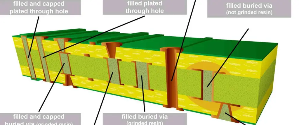
Manufacturers employ the method known as via plugging to fill holes or vias with solder masks or epoxy. Unlike via tenting, when makers fill the holes instead of covering them, this is the complete opposite.
Plugging in might be viewed as a safety precaution. During assembly or soldering, it stops additional solder substances from pouring into the soldered hole.
In simple words, disconnected vias provide spaces for unwelcome solder paste to flow, resulting in solder junctions. It’s interesting that manufacturers may plug vias with both conductive and non-conductive substances.
Also, the use of non-conductive substances to plug through holes won’t have an impact on how they work. The disadvantage is that they are not strong enough to withstand larger current loads.
On the contrary, vias that have been filled with conductive substances may easily transfer significant current loads between layers. There’s a grab, though. Conductive material-containing vias might have significant CTE.
Hence, there is a good likelihood that the conductive substance will heat up and expand more quickly than the laminate around it. However, such circumstances may lead to cracks between the contact pad and the wall.
Conductive Vs. Non-Conductive Filled Vias
· Conductive Fill
When temperature or a significant quantity of current has to be transferred from one portion of a board to the other, conductive-filled vias are typically employed. They are located underneath chips where excessive heat is an issue. Also, there will be a great deal of heat being produced. The metallic quality of the filler will typically conduct heat like a heater in many aspects, from the microchip to another edge of the circuit.
The mismatch in CTE between the surrounding laminate and metallic fille is the fundamental disadvantage of conductive-filled holes or vias. Fractures or Cracks between the holes and pads wall may result from the metal’s fast expansion and heating relative to the laminate around it. Although the fill’s goal is to increase the integrity of the metal pad, plated on holes. Conductive filled holes or vias really aren’t advised for Via or through-hole In Pad process due to this.
· Non-conductive Fill
It’s a frequent fallacy that perhaps a non-conductive filled will allow just a very faint electrical signal to travel through a via if any, electrical signal at all. It is untrue. The only change is that the fill substance is used in place of the empty space in the barrel’s space of the vias. They may still be coated with copper like every other via holes on the circuit. This is often done to stop solder and other impurities from getting into the through. Or for a via-in pad to give structural strength to a metal pad surrounding the exposed hole. A mask-plugged hole or vias is also known as a non-conductive fill.
Plugged Via Shut With Copper
This refers to an early callout that is occasionally found on heritage goods. This was originally intended to be a means to create a copper conductive stuffed via as the copper utilized to print a via sealed will also print across all copper aspects on the circuit. The challenge with this procedure involves the fact that the vias must be very tiny to make this practical. All holes and copper on the surface.
As one copper oz is equal to 1.4 mils, it takes 2.8 oz of plating to cover an eight mil drilling hole. Because the plating is used on both “ends” of the hole barrels, 8mil/2 is equal to 4. 4mil/1.4 is equal to 2.85oz. This really is 2.85 oz more copper than what is currently on the board’s surface. This would increase the overall copper weight of the design to 3.5-4 oz. With this much copper, it is impossible to create intricate trace designs or tight spaces.
The enormous difficulty in coating the hole’s whole barrel equally is another disadvantage. A hole may seem sealed, but the middle may contain trapped air or fluids that will release when subjected to assembling temperatures since the hole barrel tends to plate quicker toward the holes’ bottom and top. We won’t try this kind of fill because there are far more dependable options available.
Plugged Via Process

As previously noted, there are two ways to plug a visa. However, it varies depending on the substance (non-conductive or conductive materials). The non-conductive through plugging is much more common among these two. Now let’s examine these techniques in more detail.
Conductive Via Plugging
This plug-via method is perfect for PCBs made for applications requiring significant current transfers, often from one surface layer to the other. Moreover, conductive through plugging offers superior heat dissipation capabilities.
Pros
- Conductive hole plugging offers heat sink or transmission in places where conventional means can’t, such as the base of a chip component.
- Improved thermal conductivity results in a higher current-carrying capability. The conductivity of the substance might range from 3.5-15 W/mK.
Cons
- The pad and copper plating within the via may become unstable as a result of this operation. The disparity in CTE values between the conductive substance and overlying laminate is the cause of this issue.
- More expensive than its via-plugging equivalent that is non-conductive.
- Not that many people request conductive plugging for cables.
Epoxy Resin Or Non-Conductive Via Plugged Via
This approach is more often used than conductive ones. Manufacturers stuff the through-hole, in this instance, with non-conductive substances. A number of variables, including design specifications, accessibility, plugging machine, and CTE value, affect the plugging substance.
Nonetheless, this technique typically has a thermal conductance of 0.25 W/mK. Even yet, the plugged hole won’t convey ineffective messages or useless cash. Furthermore, it is quite challenging to distinguish between vias connected with non-conductive substances and those on a typical PCB.
Pros
- Plugging into a non-conductive via is more dependable and sturdy. These filters also have comparable CTE with laminate, unlike conducting compounds.
- It prevents solder and some other impurities from entering.
- In order to sustain active pads structurally, non-conductive through plugging is sturdy enough.
Cons
- Due to its limited thermal conductivity, it might not be able to tolerate strong currents.
Tenting Vias, Plugged Vias, & Via In Pad
While placing your PCB request, you could be unsure about the distinctions between plugged and tenting vias. Nevertheless, the following paragraph clarifies them for you.
Functionality

Tenting consists solely of covering the via holes and the circular ring with solder masks. It works especially well to avoid element exposure & lessen inadvertent shorting or contact. However, producers don’t take particular measures to guarantee that all the via holes stay closed, which reduces its functionality.
On the contrary, plugged vias include the filling process of the vias using ink. Because of this, manufacturers take special precautions to guarantee that all vias remain blocked and closed with masks. Moreover, plugging solutions do not address the aperture yellowing issue.
Via-in-pad differs from tenting and plugged vias. Drilling your vias into the footprint pad of BGA without any modification occurs during PCB manufacture. Plugged vias provide the best functioning out of the three.
Design Requirement
If the designs call for tenting files, you must provide fabrication comments. Either a readme.txt document or a design in Gerber fab can provide this information.
The Gerber fab seems to be more specific and expresses plans to take off various masks. Without this information, manufacturers can put your purchase on technical hold.
Also, if your design calls for plugged vias, you should inform your manufacturers. Similar to tenting, you may indicate it in the fabrication print or include it in a readme.txt document. You’ll also need information on the size, number, and placement of vias that you intend to plug in.
When submitting your fab notes to the manufacturer, it is essential to note the criteria for the via-in-pad.
Pros And Cons
The simplicity of a tenting procedure is one of its benefits. Manufacturers can finish the single-step procedure fast. Unfortunately, tenting does not ensure complete security.
In contrast, every plugged via is entirely filled and covered. Moreover, clogged vias could cost you more money and extra steps to accomplish.
Conclusion
Your vias must be completely protected, which calls for plugged vias. Because of their advantages despite their drawbacks, plugged vias continue to use often for soldering and assembly.
Moreover, producers have two materials at their disposal to fill PCB vias. While non-conductive materials are good for low-current devices, conductive materials are ideal for high-speed Boards. Last but not least, deliver the necessary Gerber files to avoid any problems with the producer.