How to Make a Electronic Board

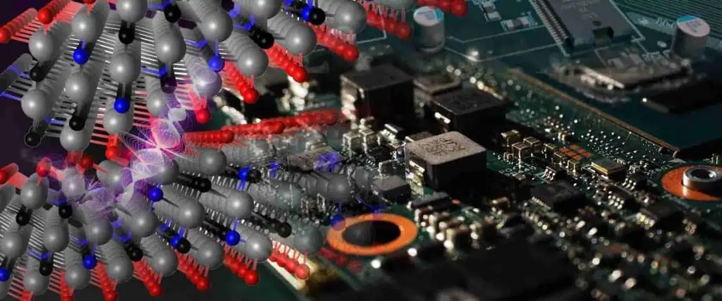
Copper conductors are used to link electronic board components electrically. These boards provide mechanical support to suit electronic gadget components. Before we go into details on how to make a electronic board, letโ€™s first consider what an electronic board means.

What Does an Electronic Board Mean?

This bare board in which you provide with the layout data as well as which, after we have given this to you, you use it to place your components is known in the industry as printed circuit board.

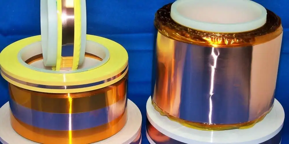
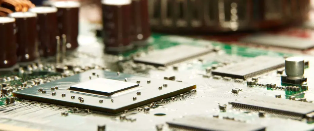
Utilizing conductive paths, tracks, as well as signal traces that are etched out of copper sheets and laminated to a substrate that is non-conductive, a PCB, is employed to electrically link as well as mechanically support the electronic components.

Whenever the board merely has copper tracks as well as features but no active devices or capacitors or resistors have been fabricated into the board’s actual substrate, then it is referred to as the PWB (printed wiring board or the etched wiring boards.

Though much more accurate but distinguishable from what can be recognized as a genuine pcb, the term PWB has generally lost favor with many people with the line between wiring and circuit gotten more hazy.

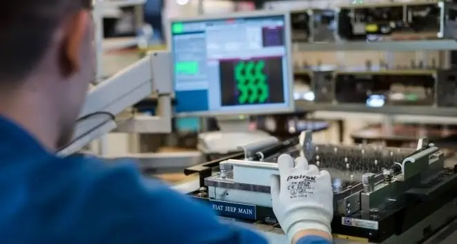
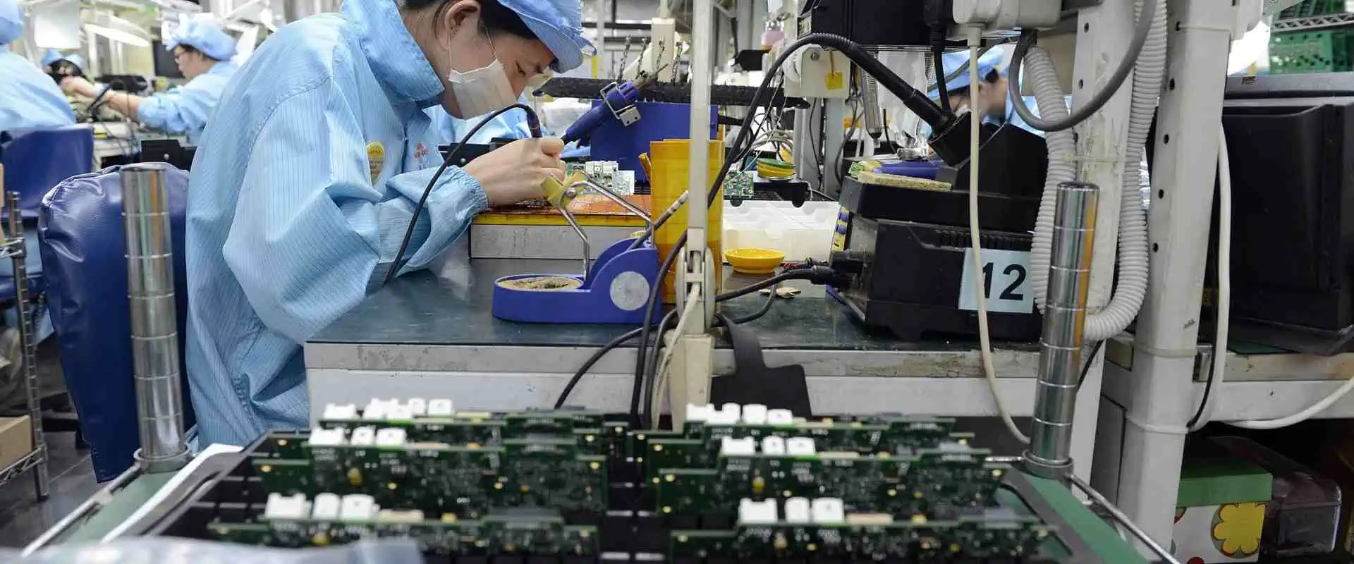
Currently, every one of the basic commercially made electronic devices employ printed circuit (wiring) boards, which enable completely automated assembly procedures that weren’t feasible or viable in older tag type processes of circuit assembly.

YouTube video

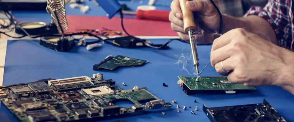
Important Steps on How to Make a Electronic Board?

Consumer Electronics Assembly

PCB Design: The Design and the Output

PCB Design

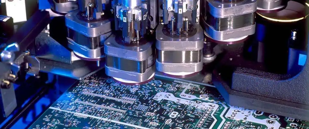
Although the stage of CAM engineer constitutes the primary step during PCB fabrication, the circuit board design can be described as the preliminary step of the process of etching.

Designers choose the proper power supplies, processors, and other components after analyzing the needs. Make a plan that satisfies all requirements.

The board must, however, be strictly consistent with the layout of the PCB that the designer generated using Circuit board design software. This contract manufacturer must be informed about the software version used for the PCB design that was used to create the circuit, as a designer, since this helps to prevent issues brought on by inconsistencies before the circuit board is made.

Print the finished design onto transfer paper. Ensure the design will fit on the paper’s glossy side.

Circuit Board Design Output

Although alternative databases and formats are accessible as well, data often comes in an Extended Gerber file called RX274x or simply Gerber), which happens to be the most used software.

Gerber files, which all store crucial information enabling synthesis, such as drill patterns, copper trace layer, component symbols, as well as other parameters, may need to be generated using various Gerber file generating processes depending on the Circuit board design program being used.

All the various components of such design are examined to make sure no problems exists after the PCB design layout has been imported in the extended gerber program.

Drawing of the PCB File – PCB Design Film Creation

The following step has to do with printing the PCB when it has been finalized. Normally, this is carried out in a dim space with regulated humidity and temperature. Punch holes within every PCB picture film layer at specific locations to align the various layers. The images for the copper routes were created with the aid of this movie.

Advice: As a Circuit board designer, please remember to inform your manufacturer to perform DFM inspection after generating the Circuit board schematic file.

PCB printing often uses a specialized laser printer termed laser photoplotter; while it’s a laser printer, this differs from a Laserjet printer in many ways. Nevertheless, this shooting method seems to be no longer adequate due to downsizing and technological innovation.

Transfer of the Inner Layer Imaging: Printing of the Inner Layer

Only boards having at least three layers can complete this step. Straightforward, two-layer boards don’t need to be drilled. Steps are added when using multilayer boards.

This preceding step’s film generation was intended to graph its copper journey. The graphics gotten from this film are now ready to be printed on this copper foil. This copper needs to be cleaned first.

Maintaining cleanliness is essential when building PCBs. After being cleaned, this copper-faced laminate gets delivered to the decontaminated area. To prevent opening or shorting of the completed PCB, be sure that there’s no dust settling on the PCB surface.

The photosensitive film coating known as photoresist is applied to its cleaning panel. This copper design is defined by the photoresist being hardened by the printer’s strong UV lamp via a transparent film.

Etching of Copper: Removing any unwanted copper

FULL PCB MANUFACTURING Quote

Etching can be described as the technique of removing surplus copper from the circuit board during PCB fabrication. All that is left on this board after removing the non-circuit copper is the surplus copper. A desirable circuit layout is therefore realized. This base copper, also known as starting copper, gets taken from the circuit board throughout this procedure.

Unwanted copper is eliminated from the board, while required copper is protected by the hardened photoresist, and the unwanted copper is removed from unhardened photoresist. To remove the extra copper, you rinse with acid etchant. Nonetheless, we still want this photoresist layer to completely enclose any residual copper.

Prior to the etching procedure, lithography is used to transfer the circuit image needed by a designer on the PCB. This creates a framework that helps in determining that part of copper that needs to be taken out.

Alignment of the Layers

The layers appear in pairs in order to create a Circuit board “sandwich,” which includes a thin copper foil layer that covers the bottom and top surfaces of the board. A “prepreg” piece would be put between every pair of layer to aid in the bonding process. Prepreg can be described as fiberglass material which has been impregnated using epoxy resin. It melts when laminated because of the pressure and heat involved. The prepreg will glue the layers in place as it cools.

Prepregs, or alternate layers of the fiberglass epoxy-impregnated sheets, are bonded with conductive cores utilizing the hydraulic press and at high pressure and temperature to create multilayer Boards. Prepreg is melted and joined together under heat and pressure. The resulting material, after cooling, will utilize the same process for manufacturing as the double-sided circuit boards.

Drilling of Holes: For the Connection of the Components

The PCB has been drilled with mounting holes, through holes, as well as other holes (which are usually inside the panel stack, with respect to the deepness of the drilled holes). Complex optics offer accurate as well as clean hole walls, which are essential.

The X-ray finder can recognize the proper drilling target point and locate the drilling target’s location. After that, drill pilot holes in the proper places to anchor the stack before drilling a succession of more precise holes.

To maintain a proper drill hole, the technician installs a buffer material beneath its drilling target prior to drilling. Its drill exit is shielded from any unintended ripping by a exit material.

AOI Inspection (For Multilayer PCBs Only)

It is not possible to detect flaws in its inner layers after lamination. Hence, before gluing and laminating, the panels go through an automated optical examination. The machine uses the laser sensor to scan the layer and compare it with the initial Gerber file so as to identify any discrepancies.

The layers must be verified for alignment after they are ready and clean. With the aid of the previously-drilled holes, the outer and inner layers will align. To keep its layers in place, the optical punch punches a pin via the hole. This process of inspection then starts to make sure there aren’t any flaws.

Final stripping and outer layer etch

Photoresist removal

pcb assembly jobs

After plating, the photoresist on the panel becomes undesired and must be removed. This is accomplished via a lateral technique that exposes the base copper of the panel to an underlying etching process for elimination while successfully removing the photoresist with a solution of soda ash.

Tin currently shields the optimal copper. Remove any unnecessary copper that is exposed and any copper that is buried beneath the remaining resist layer. In order t o remove the undesired copper during this etch, you utilize the ammonia etchant. Tin also guarantees the current stage’s need for copper.

Conducive regions and links have now been classified legally.

Solder mask

This solder mask is applied using the UV exposure procedure that is akin to photoresist to protect your board throughout assembly. All of the circuit board’s surface will be covered by the solder mask, excluding the functional parts and metal pads.

 marks for component reference as well as other circuit board markings will be silkscreened onto the circuit board asides from a solder mask. The board can be baked in the oven to cure the solder mask as well as the ink for screen printing.

The exposed metal surface of the board is going to have a polish. This facilitates soldering operations throughout assembly and protects exposed metal. The surface finish gets exemplified via HASL. Before dipping the board inside the molten solder baths, flux your board to get it ready for solder. High pressure of hot air is used to remove the excess solder out from the holes after this board has been removed from your solder bath and to smooth this solder onto the metal’s surface.

Application of a solder mask

Before applying solder resist to the board’s two sides, epoxy solder ink is put to the panel. This solder mask would let through the Ultraviolet light that the board receives. The piece that was covered is still soft and must be taken off.

The board should then be baked to cure any solder mask.

Because it is easy on the eyes, green was selected as the typical color of solder mask. All processes are manually reviewed before such a machine could inspect the PCB during manufacture and assembly. This overhead lighting that technicians utilize to examine circuit boards is beneficial for human eyes because it does not reflect the greenish solder mask.

Silkscreen

The technique of printing every important information on the surface using profiling or screen printing on the circuit board like name of company, manufacturer ID, debug points, component number, etc. This is very important when repairing and servicing.

Important information gets printed upon that board throughout this process, making it an essential phase. The final curing and coating processes will be applied to the boards after they are finished. This printing of legible identification information, such as 1-pin locators, part numbers, as well as other markings, is known as screen printing. Inkjet printers can be used to print these.

Moreover, it is the most sophisticated method of producing PCBs. In order to identify test points, components, PCBA and PCB part numbers, company logos, warning symbols, manufacturer markings, date codes, manufacturer markings, as well as almost finished boards were printed using easy-to-read lettering.

The final curing and coating stage for the PCB is at last reached.

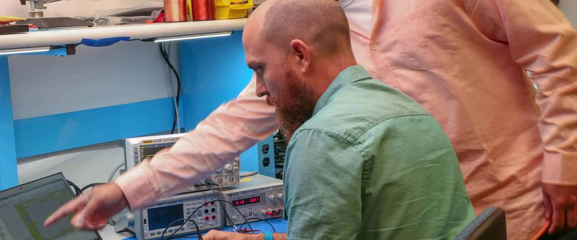
Flying probe test for electrical testing

The technician would run a functionality test of your board as a last-ditch precaution before inspection. They now perform an automated approach to verify the PCB’s functionality and conformity to the initial design.

Flying probe test, which is an advanced form of the electrical testing, is typically used to examine the electrical functions of every net on such an uncovered circuit board.

Analysis of the production and the V-score

These individual boards could be removed from this panel once the circuit board panel must have undergone electrical testing. A CNC router or machine carries out the procedure to shape as well as resize every board from a panel towards the needed specifications.

According to the total thickness of every panel, several panels could be stacked three or two high to accelerate the procedure and use router bits that are typically between 0.030 and 0.093 in size.

Using different head sizes of milling, the CNC machines may also produce grooves, bevels, and chamfers during the operation.

Final Examination – PCB Quality Assurance

The inspector must perform an extra inspection of every PCB during the process’s last stage. Check the Circuit board visually for adherence to the admission requirements. Utilizing manual and AVI visual inspection Compared to the inspection of the human eye, compares PCBs into Gerber, and yet still needs human verification.

To ensure these items meet the customers’ criteria, all orders would also be thoroughly inspected, including solderability, dimensions, and other factors. Additionally, goods on the board is subjected to a perfect quality audit before even being packed for transportation.

Typical Mistakes in Electronic Board Construction

electronic assembly soldering

There are many potential for Circuit board failure concerns to develop due to the complexity of Circuit board design as well as manufacturing processes. A number of the failures are the consequence of design errors, such as inadequate clearances or inaccurate measurements that can impair the end product’s functionality. Everyone else might be the result of manufacturing process issues, such as over-etching or drilling mistakes, which can both be disastrous.

Fortunately, the majority of these mistakes could be avoided having knowledge of the manufacturing procedure, consideration for it, and knowledge of the typical PCB manufacturing problems. Connection problems, component failure, and other concerns related to circuit board can be avoided by adhering to a variety of general design guidelines and considerations.

Plating Voids

Copper-coated holes on the PCB are known as plated through-holes. From one of the sides of your PCB to the second side, electricity can travel through these holes. This PCB board manufacturer drills these holes via the PCB board, completely piercing its base material. Then, using an electroplating procedure, a copper foil layer as well as copper coating is applied to the material’s surface as well as along these holes’ wheels.

Deposition is the procedure used in this step to deposit a thin electroless copper layer to the printed circuit board. Following this, further copper layers will be applied, and the image of the circuit is etched.

Plating voids, which are essentially holes or gaps in the circuit board plating, are usually the consequence of issues with the process of deposition. The plating voids seem to be especially problematic since through-hole plating flaws make it impossible for the electrical current to pass via the hole, leading to a flawed product.

Slivers

When making circuit boards, slivers, which are tiny wedges of solder mask or copper created during the circuit board manufacturing process, can be quite problematic. These fragments, which are frequently created during the process of etching, can happen in any of these ways explained below.

Slivers could first be created by etching away an exceptionally thin, long, characteristic of the solder mask or copper. This sliver occasionally separates before dissolving completely. Inside this chemical solution, these disconnected slivers may float around or even settle on some other board, creating an accidental link.

Cutting a part of the circuit board too deeply or narrowly is another approach to create slivers. Even when they’re intended to remain connected to the circuit board, a material of silver can entirely or partially separate from it if the etched section becomes too small or its etching is too deep, leading to either the peeled-back silver or a floating sliver. Both possibilities could have extremely detrimental effects on the functionality of your circuit board.

Acid Traps

A circuit’s acute angles are frequently referred to as “acid traps.” The acute angles help in trapping acid throughout the process of PCB etching, causing acid to accumulate in the angle’s nook, which is why they are known by this name. Because of the angle, this same acid stays in a corner that is longer than is necessary by design, eating away more material than is planned. Due to this, this acid can weaken a connection, rendering the circuit flawed and leading to subsequent, more severe issues.

The majority of designers were told to stay away from acute angles since they are conscious of the issues they can cause on the circuit board. Nonetheless, errors do occur.

Solder Mask Missing Between the Pads

The copper layer of the PCB is followed by a solder mask layers. To protect its copper traces against contact made with other metals, solder, and conductive bits, the solder mask gets placed on the copper layer’s top. Moreover, it serves as a shield between the copper as well as the environment, preventing corrosion as well as shielding the people handling the PCB from being electrocuted. Components are typically soldered onto the areas of metal known as pads that such solder board has left exposed.

This solder mask between pads may be absent entirely or partially on some printed circuit boards. By exposing excess copper than what is required, this raises the risk of solder bridges unexpectedly forming between pins while assembling.

As a result, the circuit board’s functionality and durability may be adversely impacted by a short as well as lower corrosion protection.

Copper-To-Edge Clearance Not Enough

Copper, which serves like an active constituent of PCBs, is a very conductive metal. But copper also happens to be a somewhat soft metal that is prone to corrosion. The copper gets covered with various materials to stop corrosion and guard against environmental contact.

But, if indeed the copper becomes too near to its edge during the trimming of the PCB, some of the coating may also be removed, revealing that copper layer beneath. Many issues with the board’s functionality may result from this.

Leakage of Chemicals

Another typical problem with PCBs is chemical leakage, which can occur due to the different chemicals utilized when manufacturing PCBs.

The leaking of such chemical residues over time might corrode the metal parts of the circuit boards and lead to short circuits.

Conclusion

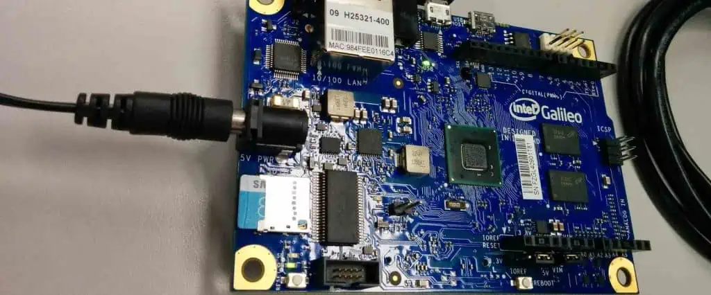
By now, you should understand how to make a electronic board. Several electrical parts make up the electronic board. Each part is essential to the operation of the electronic board. PCBs also feature holes where each electrical component needs to be installed. PCBs play a significant role in any electronic device.

Mechanism of EMI Shielding and its essential materials

pcb emi

Electromagnetic Interference (EMI)

When electromagnetic radiation from the environment prevents an electronic system or equipment from functioning normally, this is known as electromagnetic interference (EMI). EMI can come from artificial and natural sources, including electrical devices, power lines, radio and television transmissions, and natural sources like lightning.

EMI can negatively affect electronic devices, including system failure, malfunctions, and data mistakes. In addition, EMI can occasionally be dangerous, for instance, by interfering with aviation systems or causing medical equipment to malfunction.

A device’s ability to withstand an amount of EMI without malfunctioning depends on several variables, including the device’s susceptibility to electromagnetic radiation, the frequency and power of the EMI source, and the environment in which the device operates.

YouTube video

Magnetic EMI:

EMI shielding materials

Magnetic EMI (Electromagnetic Interference) is a type of interference that arises when magnetic fields created by one electronic device or circuit cause unwanted electrical impulses in another nearby device or circuit. This can occur when an adjacent circuit experiences undesirable noise or distortion due to the current created by the changing magnetic fields of one circuit.

Sources of magnetic EMI include motors, transformers, power lines, and other electrical devices that produce magnetic fields. Data mistakes, communication breakdowns, and other issues may result from interference with the performance of surrounding electronic equipment.

Capacitive EMI:

Capacitive EMI happens when electrical energy moves from one circuit to another via a capacitive coupling mechanism. For example, capacitive coupling takes place when two conductors that are separated by a dielectric material are close enough to one another for an electric field to form between them.

Capacitive coupling can introduce undesired electrical noise or interference into an electronic circuit in EMI. This interference may appear as spikes, hiccups, or other irregularities that impair electronic device functionality.

Radiated EMI:

Emissions of electromagnetic waves into the surroundings, known as “radiated EMI,” are electromagnetic interference. Transmissions from radio and television, electronic devices, and power lines are just a few examples of the many things that might produce this kind of EMI.

Surrounding electronic systems can have a system failure, data mistakes, or malfunctions when radiated EMI is present. Shielding and filtering are two methods that can help lessen radiated EMI’s effects.

Conducted EMI:

Conducted EMI is electromagnetic interference that travels via conductive paths like wires, cables, or power lines. EMI sources include switching power supplies, motors, and other electrical devices that produce high-frequency noise.

In a circuit, conducted EMI can result in malfunctions, data errors, or total system failure. Shielding, filtering, and grounding are just a few strategies employed to lessen the effects of conducted EMI.

EMI shielding

EMI (Electromagnetic Interference) Shielding is the technique of enclosing electronic devices or systems in conductive or magnetic materials to shield them from unwelcome radiofrequency interference (RFI) or electromagnetic interference (EMI).

Metals (such as copper, aluminum, or steel), conductive polymers, or conductive fabrics can help create EMI shielding. These substances form a barrier that blocks electromagnetic waves from going through and instead reflects or absorbs them.

The frequency of the electromagnetic waves, the kind of shielding material employed, the material’s thickness, and the shielding enclosure’s design are only a few of the variables that affect how successful EMI shielding is.

Applications for EMI shielding span from electronic devices like computers and cellphones to aerospace and military systems. The equipment must be free from external electromagnetic radiation interference to prevent failures.

Overall, electromagnetic interference (EMI) shielding is a crucial component of electronic design because it supports preserving the integrity and dependability of electronic systems in the presence of EMI.

Importance of EMI Shielding

FULL PCB MANUFACTURING Quote

Due to its role in preventing unwelcome electromagnetic energy from interfering with electronic systems, circuits, and devices, EMI (Electromagnetic Interference) shielding is crucial.

Electromagnetic radiation surrounds us. They can come from several sources, such as power lines, radio waves, cell phones, and other electrical gadgets. As a result, sensitive electronic components may experience malfunctions or complete failure due to this energy’s interference with their normal operation.

EMI shielding functions by erecting a wall that absorbs or blocks electromagnetic energy. Conducive materials, including metals or conductive coatings, can help to achieve this.

Medical equipment, military and aerospace equipment, telecommunications equipment, and consumer electronics are just a few examples of the many applications where EMI shielding is essential. Without adequate EMI shielding, these devices may perform worse, be more susceptible to interference, or fail.

Overall, EMI shielding is crucial when designing and manufacturing electronic systems and devices since it ensures their dependable and secure operation.

Mechanisms of EMI Shielding

Shielding from electromagnetic interference (EMI) operates by deflecting or absorbing the waves. To provide EMI shielding, several mechanisms can be helpful:

Magnetic Shielding:

Utilizing materials to prevent or lessen the electromagnetic field generated by electronic devices is known as electromagnetic interference (EMI) shielding. Due to interference or function disruption caused by EMI, electronic devices might suffer injury and perform poorly.

High magnetic permeability materials are helpful in magnetic EMI shielding to reflect or absorb the magnetic field. By forming a path of low magnetic resistance around the electronic component or device, magnetic EMI shielding helps to deflect or absorb the magnetic field.

High magnetic permeability is a characteristic of the materials used for magnetic EMI shieldings, such as nickel, iron, and cobalt alloys. Due to a characteristic of these materials known as “magnetic hysteresis,” the energy from the magnetic field can be absorbed and dispersed.

Power supplies, transformers, and motors are just a few electronic components that can benefit from magnetic EMI shielding. In addition, electronic devices can run more effectively and efficiently without interruption from outside magnetic fields by adopting magnetic EMI shielding.

Faraday Cage:

A barrier called a Faraday cage is ideal for blocking electromagnetic interference. (EMI). It bears the name Michael Faraday after the British scientist who developed the underlying idea in the early 19th century.

A Faraday cage comes from a conductive mesh of copper, aluminum, or steel grounded electrically. Electric currents are induced in the conductive material when electromagnetic waves, such as radio or microwaves, contact the cage. This conductive material creates an opposite electromagnetic field, which cancels out the first wave. This efficient EMI shield prevents electromagnetic radiation from entering or leaving the cage.

Faraday cages are helpful in several applications to stop EMI from interfering with the operation of electronic equipment and medical devices. They also shield houses and other structures from electromagnetic interference and lightning strikes.

Faraday cages are a crucial tool for many businesses that rely on delicate electronic equipment because they offer a key method for EMI protection.

Grounding:

Two related ideas help to stop electromagnetic interference from impacting electronic devices: grounding and EMI (electromagnetic interference) shielding.

An interference type brought on by electromagnetic fields is known as EMI. Radio waves, electrical circuits, and other electronic equipment are only a few potential causes of this interference. In addition, electronic devices may experience issues when EMI is present, such as signal disruption and data transmission failures.

The amount of electromagnetic radiation that can harm electronic devices decreases via EMI shielding. This shielding often consists of conductive material that may absorb or reflect electromagnetic radiation, such as copper or aluminum. To shield an electronic circuit or device from EMI, place shielding around it.

An essential component of EMI shielding is grounding. A grounded EMI shield permits any stray electromagnetic radiation that enters it to route back to the ground rather than harming the object intended to shield. The shield can be made more effective at reducing EMI by being grounded.

As a result of its role in ensuring that errant electromagnetic radiation moves away from electronic devices, grounding is a crucial part of EMI shielding. In addition, reduced interference can enhance the performance and dependability of electronic devices. Hence EMI shielding is crucial.

Absorption:

Absorption The amount of electromagnetic energy that enters a certain space or equipment can decrease using the EMI (Electromagnetic Interference) shielding technique. EMI shielding aims to build an electromagnetic barrier to prevent unwanted signals from interfering with delicate electronic equipment.

Absorption EMI shielding blocks electromagnetic radiation by absorbing and releasing it as heat. High conductivity and magnetic permeability materials, such as ferrites, metals, or conductive polymers, achieve this.

An EMI shield blocks electromagnetic waves, causing a current to flow through the shield’s material. This opposing magnetic field then traps the electromagnetic energy. As a result, the intensity of the wave penetrating the barrier reduces due to the energy coming out as heat.

The frequency of the electromagnetic radiation, the thickness and make-up of the shield material, and the shield’s design all affect how well absorption EMI shielding works. For example, the ability to absorb electromagnetic radiation will improve by using a thicker shield of high-conductivity materials.

Absorption EMI shielding is frequently helpful in stopping electromagnetic interference from interfering with the operation of electronic devices like laptops, tablets, and smartphones. Additionally, it is essential in military and industrial settings to shield critical equipment from outside electromagnetic interference.

Reflection:

In contrast to blocking or absorbing electromagnetic waves, reflection EMI shielding works by reflecting them away from the electrical device. A conductive material that reflects the waves, like a metal plate or foil, helps to do this.

When electromagnetic radiation is exceedingly intense or challenging to block using conventional techniques, reflection EMI shielding can be beneficial. However, it is crucial to remember that reflection EMI shielding may not always be successful and that other types may be necessary for some circumstances.

Generally speaking, reflection EMI shielding is a crucial way of shielding electronic equipment from electromagnetic interference and can be a valuable supplement to other shielding techniques.

Materials for EMI Shielding

Electronic equipment and devices are safe from external electromagnetic interference, which can lead to malfunctions, interference, or data loss, using EMI (Electromagnetic Interference) shielding. EMI shielding materials help prevent electromagnetic waves from spreading and lessen electromagnetic noise. High conductivity and magnetic permeability are typical characteristics of the materials used for EMI shielding, generally divided into conductive and magnetic materials.

Carbon-based materials:

Due to their special qualities, carbon-based materials are in use more frequently in EMI (Electromagnetic Interference) shielding applications. Graphene is the most promising material with its excellent conductivity, outstanding mechanical strength, and large surface area. Additionally being investigated for EMI shielding purposes are carbon nanotubes (CNTs). However, carbon-based materials can be expensive and time-consuming to produce and manufacture, and environmental conditions like temperature and humidity can impact how well they work.

Conductive polymers:

Due to their electrical conductivity, conductive polymers are a new family of materials utilized in EMI (Electromagnetic Interference) shielding applications. In addition, they are pliable, lightweight, and simple to mold into intricate designs. They can improve through doping, but the dopant’s selection and concentration can impact other qualities like mechanical strength and stability. However, oxidation or exposure to environmental conditions over time might cause a decline in their performance.

Metals:

Due to their high conductivity, metals like copper, aluminum, nickel, silver, and gold are frequently helpful for EMI shielding. In addition, because metal materials are good at reflecting or absorbing electromagnetic waves, they are frequently helpful in EMI (Electromagnetic Interference) shielding. The frequency range of the electromagnetic waves for shielding and the required shielding level will determine the thickness and size of the metal material utilized. Depending on the particular application’s needs and the surrounding environment, other materials, such as conductive coatings and textiles, can also be helpful for EMI shielding.

Common Forms of EMI Shields

A disruption caused by electromagnetic radiation that interferes with an electrical circuit is known as electromagnetic interference (EMI). Electrical devices encounter this interference, and EMI shields help to stop or lessen its effects. EMI shields can consist of conductive coatings, metal enclosures, gaskets, and absorbent materials, among other things.

Shielding Fabrics

Clothing and other textiles can benefit from EMI shielding by using shielding fabrics. These textiles can be woven into various patterns to give various amounts of EMI shielding. Additionally, they often consist of conductive materials like silver or copper. In addition, shielding materials are frequently helpful in areas like telecommunications and the military where workers face high quantities of electromagnetic radiation.

Shielding Tapes

Cables and wires can be safe from EMI by using shielding tapes. We can swap the cables in these tapes, which are commonly copper or aluminum, to create a conductive route that aids in the dissipation of electromagnetic radiation. The automotive, aerospace and telecommunications industries are just a few places where shielding tapes might be essential.

Absorptive Materials

Materials that absorb electromagnetic energy will do so rather than reflect it. These materials are frequently helpful in applications, such as power supplies and converters, where internal EMI generation occurs. Ferrites, ceramic materials containing iron oxide, are the most typical absorptive substances.

Gaskets

Gaskets are essential when two surfaces, like a door and a frame, need sealing off. They are essential in EMI shielding to provide a conductive route between two surfaces and block the passage of electromagnetic radiation. Silicone, rubber, and metal are just a few materials that can help to create gaskets.

Metal Enclosures

Metal enclosures are yet another typical EMI shielding material. These enclosures can fit a variety of electronic equipment and consist of aluminum, steel, or copper. Metal enclosures function by enclosing the electronic gadget in a Faraday cage that blocks electromagnetic radiation from entering or exiting.

Conductive Coatings

As an EMI shield, conductive coatings are frequently helpful. These coatings offer a conductive route that aids in the dissipation electromagnetic radiation on the surface of electronic equipment. Silver, copper, and nickel are the most often helpful materials for conductive coatings. We can apply these coatings in several ways, including electroplating, dipping, and spraying.

Raspberry PCB Layout: Unleash Your Imagination

Raspberry pi into a Router

The Raspberry printed circuit board is a distinctive type of printed circuit board used in producing Raspberry computers. Raspberry is a computer developed by the Foundation of Pi. Each model in the series has its unique features and capabilities. Therefore, it is essential to provide more detailed information about each of the Raspberry models.

What is Raspberry PCB Layout?

The Pi printed circuit board is a credit card-sized computer board that features a combination of castellated and through-holes with a pin header pitch. It is designed for various tasks such as word processing, gaming, and spreadsheets due to its compact size.

A Pi Foundation created the Raspberry technology, which has been present since 2012. The primary goal was to enhance learning, innovation, and experimentation. The Pi printed circuit board is the portable board utilized in Raspberry computers.

Most mobile phones manufactured in the 21st century contain Pi-printed circuit boards. ARM technology has been a common feature in many of these phones. There are two models of

Pi circuit boards available: Model B & Model A. Model A takes less power than Model B and does not have an Ethernet port, while Model B has an Ethernet port.

The Raspberry utilizes various technologies, and the development of the Pi PCB led to the creation of the computer module.

YouTube video

Customย Raspberry PCB Layout

Raspberry Pi Pico

Designing a Raspberry PCB printed circuit board involves tailoring a board to your specific requirements. This process is simple and cost-effective and can be achieved using compute module production kits. By creating a custom Raspberry printed circuit board, you can ensure that it meets your exact product specifications while retaining the highest level of design flexibility. Additionally, you can select the components you prefer using online equipment. A benefit of the Raspberry  printed circuit board is that it’s made from scratch.

Using a compute module, it is possible to design a Raspberry printed circuit board within a matter of hours. However, it is important to carefully select the functional elements you wish to include in your design. With a compute module, you can customize the layout & display ports of your custom PCB to suit your needs.

When creating a Raspberry  printed circuit board, there are several key factors to consider that will impact the requirements of your circuit board. Speed, size, memory & model type are all important considerations during the design process.

Specifications of Pi Pcb Layout

A Raspberry printed circuit board comprises numerous components, including GPIO pins, CPU, RAM, processor, & graphics chip. Additionally, this board features many interfaces for connecting with external devices. To enable startup, the Raspberry printed circuit board needs mass storage, typically provided by an SD card. It allows the board to boot up from the SD card, much like a computer starts up and loads the Windows operating system.

ยท Memory

The Raspberry Model A board has 256MB of SDRAM, while Model B has 512MB. Compared to other computers, the Raspberry’s memory capacity is relatively small. While typical PC RAM is also available in gigabytes, the Raspberry’s RAM ranges from 256MB to 512MB.

ยท GPU

A Raspberry circuit board includes a GPU, a specialized chip designed to improve image processing capabilities. The Broadcom VideoCore IV GPU is integrated into the Raspberry PCB, and it supports OpenGL for enhanced graphics performance.

ยท GPIO Pins

General Purpose Input/Output (GPIO) pins facilitate communication between the Raspberry and other electronic devices. These pins can be programmed to accept input & output commands, enabling them to communicate with various external sensors and other components. For example, a temperature sensor can be connected to the GPIO pins to facilitate data transmission.

ยท Central Processing Unit (CPU)

The CPU serves as the central processing unit, or “brain,” of the Raspberry PCB. It executes computer instructions using mathematical & logical functions. In particular, a Raspberry uses an ARM11 processor to handle these tasks.

ยท Power source connector

The shield features a minor switch on its side, and the energy source connector allows for connecting an external energy source.

ยท Ethernet Port

It is a gateway for connecting with extra devices. Using an Ethernet port, the Raspberry can connect to the house router and get internet access.

Factors to Know when choosing Raspberry Pcb Layout

FULL PCB MANUFACTURING Quote

ยท Scalability Needs

The Raspberry circuit board is not a commercial product, so there are currently no practical replacement boards available with different performance specifications. If you complete the development and then realize the demand for different specs, it’s important to consider designing for adaptability as you go from the stage of prototyping to a more flexible part of the product development process. It means planning for potential modifications and ensuring that your design can accommodate changes in performance specifications without requiring a complete redesign. By designing for adaptability, you can ensure that your product can evolve and meet changing market demands over time.

ยท Development Support You Need

The Raspberry circuit board is primarily supportable by online communities & forums, and its strength lies in support rather than professional production support. If you have tight deadlines, you can launch the product with community support. Still, if you require dedicated support, you may need to seek professional development resources.

It is advisable to schedule the components of your product and assess the level of support available before making a final decision. It is often advisable to test the performance of the components to ensure that you will achieve the outcome of your final product.

Advantages of Pi Pcb Layout

The Raspberry printed circuit boards provide numerous advantages, making them well-suited for various applications.

ยท Supports various codes

One of the most significant advantages of Pi PCBs is their versatility. But Arduino offers a more comprehensive range of capabilities. Raspberry PCBs act as single-board computers, but they also offer a Linux environment that supports coding in any language. These boards are particularly popular due to their compatibility with different codes.

ยท Peripheral support

Raspberry PCBs are equipable with GPIO pins, which are beneficial for interfacing with hardware projects. These pins offer a deeper understanding of component interfacing. The Raspberry’s abundant GPIO pins allow for the connection of multiple digital sensors.

ยท Faster processor

Compared to other boards, Raspberry circuit boards have a fast processor of 1.6 GHz. Having a faster processor results in better performance. Raspberry PCBs provide a fast processor at an affordable price point.

ยท Several sensors

The Raspberry boards come with a plethora of GPIO pins, which allows them to support multiple sensors simultaneously. As a result, they can be easily connected to various displays, modules & sensors, making them a versatile option for different projects.

ยท Serves as a portable computer

One of the most significant advantages of Pi is its portability. When combined with a display, it can function as a pocket computer. So Raspberry circuit boards support WiFi, enabling you to perform computer tasks on the go.

What are things possible with Raspberry Pi PCB?

ยท Desktop Personal Computer

A lot of individuals use personal computers for:

  • Browse the internet
  • Using social media
  • streaming movie
  • Transact online

The Pi model, 4 of raspberry, can effortlessly handle all of these lightweight processes without putting a strain on its power & processing capabilities.

While the Pi model 4 of raspberry shares some similarities with your smartphone’s hardware, the software aspect of the two differs significantly. As you may already know, Android smartphones operate on a GNU/Linux system, an open-code OS that can be customized to meet your requirements. There are various versions of the Linux OS available, and the one you have on your cell phone is one of them. On the other hand, installing the Pi model 4 of raspberry is a completely distinct version. Nevertheless, having this OS enables you to: 

  • Enjoy a desktop-class browsing experience on the board
  • Install and use apps for editing pictures, videos, and audio on the board
  • Utilize Raspberry Pi 4 for web pages, home file servers, or FTP hosts. 

Starting is simple; you only need a monitor, keyboard, and mouse. 

ยท Home Theater

Despite its small size and low power consumption, the Raspberry PCB model 4 Pi board can still support USB storage devices like hard drives. This makes it an ideal replacement for a home theater computer. 

By utilizing specialized software like OSMC, it is possible to install and utilize Xbox-style applications via KODI. Additionally, it is possible to control all functions using a remote, eliminating the need for a keyboard and mouse.

All the software needed to turn your Raspberry PCB model 4 Pi into the house theater computer is free and easily accessible online. Additionally, there is a wealth of documentation available on this topic that can assist you throughout the entire setup process. 

ยท Game Console

The Raspberry PCB model 4 Pi is significantly more powerful than older consoles, boasting more processing power. Converting your Raspberry PCB model 4 Pi into the gaming system is a simple process, requiring only the following steps:

  • Emulate the game’s software and gain access to the original program
  • Installing the game onto your Raspberry Pi 4 and enjoy playing it.

One of the most significant advantages of using your Raspberry PCB model 4 Pi as the gaming system is the ability to play games on the 4K UHD monitor.

There are numerous free gaming system options available. You can download it on your Raspberry PCB model 4 Pi, providing an unparalleled gaming experience. Additionally, you can enhance your experience by purchasing various joysticks & gamepads. With Raspberry Pi 4’s multitasking capabilities, you can play games with friends.

ยท Browsing Privacy Tool

Raspberry Pi 4 vs 3

Online advertisements are not inherently negative. Some individuals rely on these ads as a source of income, while others use them to learn about available products. But, a notable drawback of online advertisements is that they may contain trackers & malware. Should you hold the website accountable for displaying ads containing trackers & malware, or should you fault the hackers responsible for creating and implanting these trackers into the ads? The answer is undoubtedly the latter.

Fortunately, there is a solution to protect yourself from trackers & malware using a Raspberry Pi 4. With a few tweaks to the board’s settings, you can turn your Raspberry PCB model 4 Pi into an advertisement blocker. It effectively safeguarding all devices on the network from adware and malware. 

Moreover, setting up such tools is not only straightforward but also completely free. You can use different Raspberry Pi applications available online to filter incoming traffic to your devices. It is allowing only useful information to pass through and blocking the rest. 

These examples merely scratch the surface of the possibilities of utilizing your Pi model 4 of raspberry. You can explore various applications to unleash the full potential of the Pi model 4 of raspberry. If you’re a Pi model 3 raspberry and a Pi model 4 raspberry. You can even compare their performance by using them in separate projects.

Conclusion

The points mentioned above may not directly meet the requirements of a commercial product. However, for certain applications, the capabilities of the Raspberry circuit board may be sufficient. In such cases, it could be an appropriate choice for building your product.

Electronic Products made in Singapore

Audio Electronics

Singapore has a vibrant electronics sector that grows each day despite the many challenges that ravage the economy of the country in the 21st century. Actually, more than one-quarter of Singapore’s GDP comes from the electrical and electronics industry. Such statistics clearly show that this country takes the electronics sector seriously. Moreover, it demonstrates the existence of impeccable electronics manufacturing and designing companies that provide high-quality electronics products to clients.

If you are a tech enthusiast, you might wonder, which are Singapore’s most popular electronic products? And what makes electronics made in this country special?

Legendary Electronic Products Made in Singapore

Electronics panel board manufacturers

The Setron Television

The Setron television isn’t a 4K Brava TV with an impeccable display. But, on the other hand, it is the very first Singapore-made black and white television. Setron Limited was the sole assembler of these television sets. They even got pioneer status from the government since they were the first electronics firms at the beginning of an industrializing Singapore. Even though the company was importing assembly parts from Belgium, the assembly process was occurring in the factory of Setron Limited.

By the beginning of 1966, one out of six households in Singapore were proud owners of a Setron television.

The TV set was pretty bulky, and its shape resembled that of a box. Therefore people were also utilizing the television like a shelf by placing picture frames on top of the television. It was indeed a magnificent piece of tech to have at the time.

Coinafon

Before the introduction of cell phones and smartphones, people were utilizing landlines to communicate with each other remotely. The landlines were available in multiple households. Moreover, if you were out and about, you could utilize public telephones, which carried out the same function as a landline, but they were outdoors and meant for use by the general public. However, to make a call via the public telephone, you would have to either utilize a phone card or put some coins in the public telephone. The telephone could store the money you put in it, and then you could use it to make an international or local call.

Back in 1971, the popular Singapore telephone board introduced the Coinafon. A square orange payphone that was typically found near convenience stores, hawker centers, and provision shops. These phones were pretty efficient. However, these tech gadgets currently fall under the vintage category.

YouTube video

Creative Tech

Creative tech hit the electronics industry of Singapore around 1981, and they were a force to reckon with. After entering the market, the company’s goal was to deliver quality goods to its customers and explore various areas in tech. The company’s first trial electronics were the following:

  • Personal computers โ€“ their very first electronic gadgets were personal computers, including the one called Cubic T. However, the personal computers from creative tech were not a big hit, so the company had to move on to another product.
  • Sound cards โ€“ after flopping in the development of personal computers, creative tech pivoted towards developing high-quality sound cards for personal computers. The sound cards from this company became a great hit in silicon valley, and pretty soon after, the sound blasters from creative tech became the de facto standards for all audio-processing PC cards.
  • MP3 player โ€“ after their success with the sound cards, creative tech began to invest heavily in audio gadgets not long after the company took to the market to launch their first MP3 player, which was a huge success.

As of the 21st century, creative tech still develops impeccably high-quality audio gadgets for its customers.

The ERP and In-vehicle Unit

The ERP (electronic road pricing) and in-vehicle unit is a popular transportation innovation that the government utilizes in Singapore. Instead of simply placing multiple toll booths, the government of Singapore installs dynamic ERP tolls which bear charges that change according to various elements such as:

  • Congestion
  • Time

The very first in-vehicle unit (which works seamlessly with the ERP tolls) hit the market back in 1998. Since then, vehicle assembly companies in Singapore have been installing them in all Singapore-registered cars. Moreover, according to the government of Singapore, every vehicle in Singapore should have these devices.

USB Thumb Drives

After inventing multiple gadgets that were influential to the world in the 20th century, Singapore was not done. In 2000 a company in Singapore known as Trek developed the first-ever Thumb drive and put Singapore on the map. Of course, there are other companies that make thumb drives today, for example, IBM. However, the very first thumb drive was generated in Singapore by Trek.

As we move into an era of cloud storage, thumb drives are slowly becoming a thing of the past. However, the legacy of Trek will never be forgotten.

Infrared Fever Screening

FULL PCB MANUFACTURING Quote

After the SARS outbreak scare, which took place in 2003, Singapore was not going to take a chance in terms of defending themselves. So, after a short period, Singapore tech electronic and the DSTA (defense and tech agency) came together to generate the famous infrared fever screening system.

The infrared fever screening gadget simply utilizes heat loss mechanisms and wavelengths to effectively screen many people at once and then determine whether or not individuals in that group have a fever.

Razer

 Razer Inc is a Singapore electronics manufacturing company that is responsible for the production of high-end personal computer gaming mice known as Boomslang. The Boomslang mouse has been a great hit in the tech industry. However, this is not the only electronic gadget that this company produces.

Razer also generates variations of the chic RGB-lit keyboards and mice. Moreover, this company also generates various other electronic components, which include:

  • Phones
  • Laptops

Moreover, the company is also looking to launch toasters. Therefore you can expect to see more of this company in the near future.

X-Mini

Regarding wireless communication gadgets, Singapore hasn’t been left behind either. For example, the classic X-mini rode wave Bluetooth speaker is a portable Bluetooth speaker that hit the electronics market of Singapore and the world like a gigantic wave. XMI, a company In Singapore, is responsible for manufacturing these incredible speakers that revolutionized the audio scene.

The X-mini is tiny such that it can fit in your pocket. However, even though it is tiny, it still has impeccable audio quality, and it lives up to the company’s mantra, which states, ” great sound in small forms.”

Top Electronic Manufacturers and Designers in Singapore

In the discussion of Electronics products made in Singapore, we can’t leave out the many electronics manufacturers and designers that make these products. Here is a list of the top electronics manufacturers and designers in Singapore:

C and M Electronics Engineering Services

C and M is an electronics manufacturing company that offers impeccable consultation and designing services besides product manufacturing and development services. Moreover, this company also provides repair services for various electronic products.

C and M come as a well-certified company, and it delves into the following services:

  • Commissioning
  • Product development
  • Circuit board consultation
  • PCB fabrication

The headquarters of this company are in Yishun, Singapore.

Company Highlights

Generally, C and M has the following main features:

  • It offers custom services
  • It complies with multiple industry regulations
  • The company also deals with printed circuit boards and various other electronic variations
  • Lastly, C and M provides commissioning, development, fabrication, and consultation services

Products Provided by C and M

C and M generally provide the following products to their customers:

  • Door closing Bells โ€“ two variations (A and B)
  • Bus stop display units
  • Solar battery charge controllers
  • Digital announcers
  • Volume control units
  • PWM tension controllers
  • AC and DC Power Inverters
  • Door Control Units
  • Message Selector Units
  • PIW Buzzer
  • DC Motor Speed Controller
  • Bus stopping bells
  • Door-closing display units
  • Triangle bus-stopping display units
  • Auto door controllers
  • Seven segments LED displays
  • Arrow light controller and control
  • 60 Amperes DC Converter
  • 14 and 3 channels Thyristor Drive Running Lights

Design Tech NYC

Design Tech NYC hit the electronics industry around twenty years ago, and since then, it has become one of Singapore’s most popular electronics manufacturing companies. Generally, this company is renowned for offering impeccable electronics designing solutions for the IT industry. However, this company primarily majors in mac desktops and design environments.

Design tech  NYC generally comes as a  certified reliable solution provider for most, if not all, electronics design needs

Company Highlights

Design tech NYC mainly stands out due to the following reasons:

  • Its impeccable training services
  • How it utilizes a client-centered approach when providing its services
  • Over twenty years of experience in the electronics industry

Services Provided

If you plan on working with design tech NYC, then you will enjoy the following services:

  • Design vault
  • High-quality training services
  • DT helpdesk
  • Design check
  • Design care

Micron

Micron is an electronics manufacturing company in Singapore that has a remarkable reputation. Moreover, this company is highly rated when it comes to producing high-quality electronic solutions and products.

Micro has over 40 years of experience in the electronics market since it hit the industry in 1978. And this company utilizes this experience to provide impeccable services to diverse sectors. Moreover, this company offers high-quality and reliable manufacturing and design services, especially regarding memory and storage systems.

Company Highlights

pcb assembly jobs

When compared with other electronic manufacturing and designing companies in Singapore, Micron stands out due to a couple of reasons which include:

  • Its experience in the electronics industry which surpasses 40 years
  • Its compliance with multiple industry regulations
  • Over 13 electronics manufacturing sites
  • Up to 17 global locations
  • How it provides high-quality storage and memory systems

Products Provided

Micron generally offers the following products to its customers:

  • Heterogeneous memory storages
  • Advanced computing solutions
  • Memory cards
  • Advanced solutions
  • NOR Flash
  • SSDs NAND Flash
  • Multi-chip Packages
  • Managed NAND
  • Ultra-Bandwidth Solutions
  • Authenta Security solutions
  • DRAM
  • The DRAM Modules
  • DRAM technology

ST Engineering

ST Engineering is another famous electronics manufacturing company that has its roots in Singapore. The company is primarily renowned due to its innovation and ability to adapt to emerging technology. Moreover, ST Engineering provides superb manufacturing and design solutions for all your electronics needs. By utilizing expertise and innovation to drive its operations, ST engineering is able to provide impeccable design and manufacturing services.

ST Engineering has a well-trained workforce that it utilizes together with world-class gadgets to guarantee high-quality outputs each time. Moreover, this firm presents itself as a global engineering, technology, and defense entity.

Company Highlights

When you compare ST Engineering with other electronics manufacturing companies, you will note that this company stands out due to the following reasons:

  • It utilizes a collaborative approach when it comes to dealing with various clients
  • ST is compliant with multiple industry and sustainability regulations
  • And lastly, ST targets multiple sectors and industries, which include public security, digital tech, defense, aerospace, and smart cities.

Services and Products Provided by ST

Generally, ST Engineering company provides multiple services and products in regard to the electronics industry, and some of them include the following:

  • Critical infrastructure
  • BPO transformation
  • Cyber security solutions
  • AI, data science, and analytics
  • Defense-related solutions, for example, intelligent facilities, C5ISR, et cetera
  • Commercial, vessel, and naval intelligence
  • Naval
  • Environment Engineering
  • Satellite Solutions
  • Urban Solutions
  • Aviation Asset Management
  • Aero-structures
  • Aero systems
  • Aerospace MRO

Conclusion

Singapore is one of the many countries that take the electronics industry seriously. Moreover, this country invests heavily in the growth of the electronics industry; hence we see it encouraging upcoming firms like Setron to make an impact in the electronics world. However, their investment in the industry also pays off since we can see the company gaining huge returns from the sector. On the other hand, electronic manufacturers and designers are also playing a significant part in the growth of the electronics industry in Singapore. We hope this article has provided you with all the information you were looking for regarding electronic products made in Singapore and the manufacturers that make them possible.

The Scope of Operations in Kentronics Engineering Services & Supplies Company

through-hole assembly process

Engineering services and supplies are important aspects of technology. There are several engineering services and supplies companies out there. However, there are some disparities in the way these companies operate. However, it is important to understand what engineering services & supplies companies do.

Engineering services & supplies companies offer specialized consulting services that help in introducing technology or product to the market. These companies vary in terms of the services they provide and as well as the capability. While some engineering services and supplies companies offer consultation and take responsibilities for the whole project, some companies only offer construction management.

Finding a reputable and reliable engineering services & supplies companies can be a daunting task. A good engineering services and supplies company doesnโ€™t just take up an engineering project, they offer services beyond that. Kentronics is one such company. Our main focus is on Kentronics engineering services & supplies company.

What Does Kentronics Engineering Services & Supplies Company Offer?

7 layer pcb assembly

Kentronics Engineering Services & Supplies Company is a well-known company in the engineering field. This company was founded in December 1993. It started with the provision of PCB design or layout services to PCB industry market. This company has invested in their services and extended them beyond PCB layout or design.

It ventured into services like printed circuit board assembly and printed circuit board manufacturing. Presently, Kentronics is a leading PCB design manufacturer that offers turnkey and quick turn services fir high performance and high-technology circuit boards in Asia Pacific.

Kentronics Engineering Services & Supplies Company has its headquarters in Singapore where it employs a large percentage of workers. The main business enterprise of this company is PCB manufacturing with electronic parts. ย Also, Kentronics engineering services & supplies company provide engineering consulting activity that integrates various services solutions for the development of a product.

This company is responsible for an engineering project as regards the assessment, creation, testing, and simulation of the product. Kentronics ensure expertise in all relevant codes and standards.  Their process for testing and fixing modules is top notch and reliable. Thousands of operators across Australia trust this process.

The Kentronicsโ€™ team of professional engineers and developers focus mainly on offering positive results for all their customers. This company takes pride in the reputation they have built. Kentronics has been able to build a good reputation based on the vast expertise of their dedicated team and a high level of service.

Kentronics integrate a reliable and unmatched process for testing modules. Also, this company offers excellent value for your money. Quality service and smooth delivery are the key factors to this companyโ€™s success. The team at Kentronics are committed to servicing the engineering industry.

Services Rendered by Kentronics Engineering Services & Supplies Company

FULL PCB MANUFACTURING Quote

Engineering services & supplies companies differ in terms of scale, capacity, and organizational structure. Many engineering and supplies companies offer a wide range of services. Kentronics engineering services & supplies provide full support on programs and are a great choice for customized services.

Below are some of the engineering services offered by Kentronics.

Simulation and Testing

At any phase of product development, there is a need for trial testing and runs. This trial testing gives answers to various questions. Also, it helps to know if the product will deliver what it is expected to. Modeling and analysis helps in addressing some questions. The testing and simulation procedures needed for evaluating a part or component take a lot of time. These procedures need to be properly and carefully carried out to ensure the efficiency of the final product.

Engineering consultation

This is one of the services offered by Kentronics Engineering Services & Supplies Company.  An engineering services and supplies company should provide technical consultation regarding research and design services. Offering support for moderate rapid prototyping, automation, and technical documentation services rendered by Kentronics.  Also, this company hires a team of professional and dedicated engineers that help customers to develop a comprehensive project plan.

Reverse engineering

Reverse engineering involves removing a final product and deciding its performance. The data collected from the completed product could help provide further input into a new product. when it comes to reverse engineering, the engineering designs a CAD physical model and gathers data from it. Companies will then use this data to improve or redesign the object. For instance, customers leverage the reverse engineering services provided by Kentronics to enhance the performance of production and upgrade a component.

Design and Development

New product development is a popular service offered by most engineering services and supplies companies. Also, known as research and development, Kentronics integrates skilled technical support for product design and development to ensure products get to the market faster. Research and development entails introducing a project to highly skilled developers and transforming this idea into valuable final products.

Kentronics offer design supervision services for various solutions. This will include maintaining good communication with the contractor and agreeing on the final characteristics and design.

Technical documentation

Technical documentation involves documenting the structure and specification of a product. Also, it involves documenting important development goals. For any engineering project, there is a need for documentation.

Benefits of Partnering with Kentronics Engineering Services & Supplies Companies

Assembly Testing

Kentronics engineering services and supplies company has great engineering expertise and skills. Asides from that, this company has experience in providing a wide range of engineering services. It is important you know the benefits you would get to enjoy when you partner with a company. Also, this will help customers to create their own expectations to know how to maximize the benefit from this collaboration.

Permanent innovations

It may be very difficult to introduce novel technologies and strategies in the fast-growing engineering industry. One crucial thing that can enhance solution design and also reduce budget is advancements. Also, advancements guarantee a more improved outcome. However, resources and expertise are required when evaluating every enhanced solution before incorporating it into a project. Not all engineering services and supplies companies possess the necessary resources and demands.

Furthermore, when you work with Kentronics engineering services and supplies company, there are no restriction when it comes to solutions and approaches. Kentronics is an experienced engineering services company that offers creative innovations in the engineering field.

Fast-track solution design

Engineering services and supplies companies always need to facilitate a solution release. Also, these companies may have to offer operability by a particular timeline. This scenario usually requires an efficient response from the engineering team. However, creating a new in-house engineering team will require much supervision and time. Therefore, Kentronics provide an active and well-skilled staff pool that help to enhance solution development as soon as possible.

Specialized skills

Kentronics has expertise and skills in providing engineering services and supplies to their customers. These days, businesses in complicated sectors like electrical engineering find it difficult to hire engineers. This is because the cost of labor makes it difficult to hire full-time staff. Also, the labor market entails competition which is unhealthy for professional engineers.

Kentronics maximize unique engineering qualifications when needed. This engineering service company has show proven case experience in various sectors, which enables it to implement best practices that resulted in prosperity identical solutions.

Customer support

One of the benefits of partnering with Kentronics is the access to customer support. Customers can gain access to support services. This company offers ongoing support to their customers regardless of the time. With this, customers can gain access to the company from anywhere at different time zones without having to wait till the next business day.

Faster turnaround time

Speed is a major concern for customers who need engineering services. Kentronics engineering services and supplies company offers faster turnaround time to customers. Almost 23 percent of companies prefer to outsource their engineering project to engineering services company that offer a faster turnaround time. Kentronics has a team of professional engineers who are always working around the clock to deliver the best. Also, this company doesnโ€™t compromise quality for speed. Due to its dedicated team of engineers, Kentronics is able to meet the demands of their customers at a faster speed.

Certification

Kentronics believes that the idea of an engineering project is paramount to their client and as such makes effort to ensure the project complies the vision of the client and as well as the industryโ€™s standards and codes. This company is ISO 9001 certified. This company prides in the quality of their products.

More Facts about Kentronics Engineering Services & Supplies Company

Box Build ASSEMBLY

Kentronics offers extensive consultation and expert advice on engineering projects. Also, this company can take charge of a project and make efforts towards evaluating, designing, and testing the product. Basically, Kentronics works with responsible engineers who are ready to deliver the best. Introducing a project to market can require, scoping and buying some materials.

Developers and engineers work out these details during the design stage. Kentronics feature in-house procurement departments. Also, this engineering services company offers knowledge about all the important standards and code. An engineering project without compliance with standards and codes is nothing to write home about.

Kentronic work with various organizations in different industries. Therefore, this enables this company to acquire more knowledge and experience as regards some particular standards and codes in the industry. Kentronics ensures the design of the project complies with the regulations for a particular jurisdiction.

With more than two decades of providing engineering services and supplies, Kentronics offers specialized engineering consulting to provide solutions to any engineering project. Furthermore, this company offers integrated engineering services to customers. Also, this company can carry out a study to create a master plan for long-term projects.

Kentronics integrates streamlined testing protocols which enables them deliver top quality work at very affordable prices. Furthermore, this engineering services and supplies company has set up quality objectives which are constantly improved. Since 2013, Kentronics has met the ISO 9001 certified. This ISO certified company complies with certain ISO standards in the industry.

One of the amazing things about this engineering services company is that it creates lasting and close  relationships with manufacturers. Hence, this allows them to deliver quality services even in challenging conditions.

Why Kentronics Engineering Services & Supplies Company?

  • Kentronics integrate a reliable and unmatched process for testing modules. Also, this company offers excellent value for your money. Quality service and smooth delivery are the key factors to this companyโ€™s success.
  • This company is capable of fabricating different types of printed circuit boards ranging from rigid-flex, rigid, and flexible boards.
  • Kentronics offers PCB assembly service which includes through hole, surface mount, and wave soldering. Also, its circuit boards are inspected using the X-ray inspection.
  • Kentronics provides technical consultation regarding research and design services. It offers support for moderate rapid prototyping, automation, and technical documentation services.  Also, this company hires a team of professional and dedicated engineers that help customers to develop a comprehensive project plan.
  • Kentronics integrates skilled technical support for product design and development to ensure products get to the market faster. Research and development entails introducing a project to highly skilled developers and transforming this idea into valuable final products.
  • Also, this company doesnโ€™t compromise quality for speed. Due to its dedicated team of engineers, Kentronics is able to meet the demands of their customers at a faster speed.

Conclusion

A good engineering services and supplies company doesnโ€™t just take up an engineering project, they offer services beyond that. Kentronics is one such company. This company partners with the internal engineering team of their client. Also, they partner with different project stakeholders in providing quality services.

The team at Kentronics know the right steps to take to enable the success of your project. Your project will work out as planned without any stress when you choose Kentronics. This company has a solid reputation in the engineering services and supplies industry. The team here is committed to offering the best to their clients. Furthermore, Kentronics is transparent with their clients as they believe transparency is a good policy.

Key Features and Benefits of IBM IoT Platform

IBM IoT

The Internet of Things (IoT) comprises interconnected entities with each offering a particular degree of adaptiveness, behavioral autonomy, and communication with other connected devices. Connectivity may integrate various topological forms and integrate complex network that connects these things to the Internet via the use of proprietary communication protocols.

When we talk about things, they could be virtual or physical. They all have a programmable representation in the digital world. Also, they can reach the physical world though actuation/sensing capabilities. Details such as status, location, or identity of the thing are included in the representation. These things provide services with or without the need for human intervention.

IoT has to do with the physical devices connected to the internet. These devices are all receiving and transmitting data. The integration of IoT data with IBM Cloud technologies makes it possible for businesses to get valuable insights to enhance almost all aspects of their operations and as well ensure innovative, new business models.

YouTube video

What is IBM IoT?

IBM IoT PCB
IBM IoT PCB

To understand IBM IoT, one needs to understand what IBM offers and what type of organization it is. IBM stands for International Business Machines Corporation. As one of the worldโ€™s largest technology companies, IBM has operations in over 170 countries and more than 345,000 employees across the world.

This giant technology company specializes in the production and distributing of computer software and hardware. Also, it designs cloud computing and data analytics. Over the years, IBM has served as a research and development corporation with inventions such as UPC barcode, floppy disk, and the hard disk drive.

Key Areas where IBM IoT is conducting Strategic Work

IBM has invested in research and development of the Internet of Things. Furthermore, strategic work in IoT has been performed in key areas.

In the Edge area, IBM IoT is addressing issues in which privacy, security, bandwidth, or latency canโ€™t allow data to be moved to a cloud platform. There is a great need to analyze and process IoT information at the edge, close to where the data was generated. Furthermore, the research in edge are gives considerations to challenges being faced in the data analytics and IoT application domain.

External research communities address this issues in concepts like mobile computing for telecommunication networks  and fog computing for data networks.

In the Platform area, IBM is making research about technologies that can produce a scalable platform for IoT and offer support to the requirements of the IoT domain. The IoT domain features a workload produced by devices and sensors. Also, it needs more adaptive real-time data processing and more scalability.

As regards the Solutions area, IBM is providing new solutions that are integrate cognitive computing technologies in the edge and cloud context, to provide new IoT solutions. Therefore, this will include developing new solutions for elderly wellness, cognitive dialogs, cognitive buildings, home insurance, Industry 4.0, IoT data discovery, home insurance, and other solutions in industries.

The Internet of Things research are by IBM spans across various labs in the world, with major activities in India, Australia, Dublin, and China labs among others.

IBM IoT Connected Vehicles

FULL PCB MANUFACTURING Quote

IBM has extended the power of AI and data analytics to internet connected cars. The IBM IoT Connected Vehicle Insight uses real-time data about vehicles, drivers, and the surrounding to maximize in-car experience. This cloud service streams data from the sensors of vehicles and then integrates AI and analytics to have an idea of the driver behavior.

Also, it connects with other data systems in the cloud like traffic and weather, to add situational awareness. This information helps connected vehicles to easily detect problems with quality or safety and then carry out immediate action.

For instance, the collision avoidance system of a vehicle can improve when connected to real-time traffic and weather conditions. Also, the SaaS platform offers enhanced navigation features like destination prediction, according to particular driver patterns.

What are the key features of IBM IoT Connected Vehicle Insights?

The IBM IoT connected vehicle insights offers some basic features which include:

  • Vehicle insights and event detection
  • Integration with third-party data, APIs and apps
  • Product quality improvement
  • Dedicated SaaS environment
  • Designed for modern systems and standards

Key Benefits of IBM IoT Connected Vehicle Insights

Optimization of arrival times and driver convenience

IBM IoT Connected Vehicle provides navigation features, map context, and optimal routing which help in improving the driverโ€™s journey. The navigation features provided by this platform consider weather conditions, driver patterns, and real-time traffic.

Improvement of product quality

Also, this IBM IoT platform monitor data all through the life span of a vehicle to optimize production and engineering and as well detect malfunctions.

Ensure the safety of drivers

Vehicle systems can easily identify unsafe policy variations or practices by having access to real-time insights of driver behavior. This helps in responding effectively to any problem.

Improvement of revenue streams and business models

One of the benefits of the IBM IoT connected vehicle insight helps in enhancing revenue streams and business models.

IBM Watson IoT Platform

The IBM Watson IoT is a project developed by IBM. This project was initially aimed at designing a natural language-responsive system where questions asked in a human language can be interpreted and then answers can be analyzed. This system would provide answers to questions that it would take researchers time to get answers.

What is the IBM Watson IoT Platform?

The IBM Watson IoT Platform connects gateways, applications, and devices  for IoT solutions. Also, this platform provides support for MQTT and REST protocols for administrative functions, applications, event processing, devices, and gateways. You will find The IBM Watson IoT Platform on the IBM Cloud platform which was once known as IBM Bluemix.  Also, the IBM Cloud platform works based on Kubernetes and Cloud Foundry.

The IBM Watson IoT platform helps you to manage connected devices so users can have access to historical and live data. There are several features offered by the IBM Watson Platform. These features include:

Dashboard

When you gain access to this platform, you will see the dash board. The dashboard of the IBM Watson IoT platform comprises a number of cards and boards that offer different visualization options for IoT solution. To get familiar with the dashboard, you can explore the cards and boards. Also, the dashboard is user-friendly. Therefore, it makes it easy for users to navigate.

Devices, gateways, and applications

The device management control system is another feature the IBM IoT platform offers. With this feature, users can develop and remove devices, gateways, and applications. Also, this feature helps users to check and enable actions in the device, like a reset or a firmware upgrade request.

API keys can be created to ensure applications connect properly to the IoT organization and communicate with the other components.

Security

IBM IoT platform can help in managing the security aspects of a solution. This may likely include checking the rules of a country, designing policies for device connections, and providing white and black lists for the IP address of a device. Also, you can have control over users allowed or prevented from managing the IoT organization.

Benefits of IBM IoT Platform

IBM IoT platform helps users to start their IoT project quickly. This cloud-hosted platform is designed to make users easily derive value from their IoT devices. Also, it offers capabilities like IoT data storage, device registration, and IoT data connectivity. Below are benefits of the IBM IoT Platform:

Management and connection of devices

You can easily connect to the IBM IoT platform and then connect and manage your IoT devices. Also, users can create their own mobile IoT apps and visualization dashboards.

Enables team development

The IBM IoT platform enables team development of IoT. This is because IBM IoT enables the development of AI technologies in addition to the facilities provided by this platform.

Easy interaction with the platform

This platform is a very easy one to interact with. All you need is to understand the structure of the platform. Also, it allows you to easily navigate around each devices.

Active performance management

One of the benefits of IBM IoT Platform is its analytic capabilities to detect new correlations and as well search and know signatures in data in order to figure out operational problems with equipment.

How IBM helps you get the Best Value from Your IoT Data

The journey of IBM IoT has evolved over the years. However, it is indeed a journey during those years. Here are ways organizations can get value from their IoT efforts.

Collect data

Collecting data from your devices is important. At first, when IoT was introduced, we were surprised what we could achieve with this technology. When we discovered we could get things like light bulbs connected to the IoT. Also, we realized this connectivity could help us turn on and off these devices. This is why it is important you collect data into a usable format.

Pattern Visualization

Businesses increased their expectations as IoT matured. Therefore, the focus shifted to pattern visualization. It isnโ€™t all about turning off and on the bulb conveniently, but how the connected light bulb provides data on how it is being utilized. With this data, you can understand your bulbโ€™s energy usage and how to regulate it. For instance, you can decide to dim your lights to keep energy usage on check or decide not to light up some places at a particular time. Businesses need to have a clear understanding about the patterns in their data.

Advance to analytics

Analytics can make data smarter as it enables you to have real-time data about your IoT device. It gives you a better picture of the happenings in your devices and environment. Also, it enables you to identify patterns and predict outcomes. In the long run, this will help you in adopting new practices that would help you prevent possible problems.

More Facts about IBM IoT Platform

embedded iot

The IBM IoT platform offers a straightforward and simple user interface where devices can be managed easily and simply. Also, users can add devices and control any access to their IoT service. This platform helps users to monitor the usage of their data. As a cloud-hosted service, IBM IoT helps you to derive value from IoT devices.

The device management service provided by this platform enables users to carry out device actions such as firmware update or reboot, get metadata and device diagnostics, or execute bulk device removal and addition.

Users can also receive and send commands to their devices. They can achieve this by integrating MQTT with TLS to enable communication between their devices and IBM services. IBM IoT platform offers data lifecycle management. This means that users can access real-time data from their devices. They can as well choose to store data for a desired period. This allows users to gain access to historical data.

Security is a crucial aspect of IoT deployment plan. Also, security by design is what everyone integrating IoT should think about. This entails that IoT devices and software are safe for end-users and manufacturers.

This is why IBM IoT security framework is protecting IoT devices and data from potential risk. IBM Watson IoT platform integrates security by design in its infrastructure and platform. It is a big deal to have access to IoT devices and firmware. The ability to view, manage, and update.

IoT risk and security management is a big challenge that needs to be addressed as soon as possible. Also, protecting the IoT infrastructure is a priority for enterprises.

Conclusion

The IBM Watson IoT Platform connects gateways, applications, and devices  for IoT solutions. Also, this platform provides support for MQTT and REST protocols for administrative functions, applications, event processing, devices, and gateways. You will find The IBM Watson IoT Platform on the IBM Cloud platform which was once known as IBM Bluemix.

The IBM IoT platform enables team development of IoT. This is because IBM IoT enables the development of AI technologies in addition to the facilities provided by this platform. The world has experienced a big change since the introduction of IoT.

Definition of Microsoft IoT and its importance in todayโ€™s digital landscape

Microsoft IoT PCB

It seems like everyone is talking about IoT these days. Its advantages, disadvantages, privacy issues, security problems, and significance are all discussed. In a time when every part of our life depends on technology, itโ€™s crucial to grasp the value of IoT.

The IoT, depicts physical items that connect and share data with other devices and systems across communications networks. It refers to integrating digital technology into the natural environment. It is a bridge between the real world and the digital one.

IoT is significant because technology makes connecting numerous systems and equipment in previously impractical ways feasible. As a result, it opens up new possibilities for automation, data collection, and analysis. IoT makes it possible to monitor and control systems in real-time, increasing productivity and cutting expenses. It can also make possible new business models like subscription-based services and product-as-a-service offerings.

https://www.youtube.com/watch?v=n0LqqadplIA

How Microsoft IoT works

A group of Microsoft-managed cloud services known as Azure IoT connects keeps track of and manages billions of IoT assets. Azure IoT is a platform featuring several Microsoft-managed cloud services. It allows enterprises to connect, monitor, and control different IoT assets. In addition, Azure IoT enables hosting for all sorts of IoT applications and connecting, storing, and analyzing data from field devices. Azure IoT provides a versatile option for enterprises wishing to send their IoT process data to the cloud. As a result, it supports connections to data loggers and other edge devices from various vendors.

IoT-based solutions could be created with Azure. It offers scalability, easier and more affordable device maintenance, and monitoring devices at a single location, Azure IoT Hub. Additionally, it provides various services for creating, managing, and carrying out various tasks on IoT devices registered with the cloud.

Advantages of using Microsoft IoT

There are several advantages of using Microsoft IoT, some of which are:

  • Easy development and deployment of IoT applications thanks to Microsoft IoTโ€™s good integration with other Microsoft services like Azure, Power BI, and Office 365.
  • Wide range of device support: Windows, Linux, and Android are just a few platforms and devices with which Microsoft IoT is compatible. This makes it possible for developers to create solutions for various IoT scenarios.
  • Security: To prevent unwanted access to data and devices, Microsoft IoT delivers strong security features like authentication, encryption, and access control.
  • Scalability: Microsoft IoT is appropriate for enterprise-level IoT solutions since it can scale to accommodate large-scale installations and manage millions of devices and messages.
  • Analytics and Insights: Organizations can use Microsoft IoTโ€™s strong analytics and insights capabilities to glean insightful information from their IoT data and make wise decisions.
  • Developer-friendly: Microsoft IoT makes it simple for developers to create and deploy IoT solutions by providing various development tools and frameworks, including Visual Studio, Azure IoT Hub, and Azure IoT Edge.

Microsoft IoT generally delivers a strong and adaptable platform that enables businesses to successfully develop, implement, and manage IoT solutions.

Step-by-step guide on building an IoT solution using Microsoft IoT

FULL PCB MANUFACTURING Quote

Determine the IoT scenario you wish to use

Finding the scenario you want to use is the first step in developing an IoT solution. This may involve anything from tracking the whereabouts of a fleet of vehicles to keeping an eye on the humidity and temperature in a greenhouse. Once you have determined your situation, you can move on to the following stage.

Pick your equipment

The following stage is to decide on the hardware youโ€™ll employ to gather and send data from your IoT devices. Numerous devices, including the Raspberry Pi, Arduino, and other single-board computers, are supported by Microsoft IoT. But first, you must select the most appropriate hardware for your situation.

Configure your IoT hub

An IoT hub is a cloud-based service that is a focal point for data transmission from your devices. You must set up an IoT hub in your Azure account to receive data from your devices.

Connect your gadgets to the IoT hub

You can link your gadgets to your IoT hub once configured. This entails setting up your devices to communicate with the IoT hub over a protocol like MQTT or HTTPS.

Set up your data pipeline

The setup of your data pipeline is the following phase. First, setting up your IoT hub to provide data to other Azure services like Azure Stream Analytics, Azure Functions, or Azure Event Grid is required. These services can analyze your data in real-time or start actions depending on certain circumstances.

Visualize your data

The visualization of your data is the last stage. Microsoft IoT offers a variety of tools, such as Power BI, Azure IoT Central, and personalized dashboards made using Azure Web Apps to assist you in visualizing your data. As a result, you may obtain insights into your IoT scenario and make data-driven decisions by visualizing your data.

Key considerations when building IoT solutions with Microsoft IoT

IIoT

Security:

Any IoT solution must consider security. Microsoft IoT provides several built-in security capabilities to help safeguard your devices and data. Utilize these capabilities and adhere to established practices for protecting your devices and data.

Scalability:

As your device fleet expands, itโ€™s critical to make sure your solution can scale to accommodate the huge amounts of data that IoT solutions might produce. To manage high volumes of data, plan your solution with scalability in mind and consider leveraging Azure services like Azure Stream Analytics and Azure Functions.

Interoperability:

Itโ€™s crucial to ensure your IoT solution is compatible with other technologies as it may need to integrate with other devices or systems. Select technologies that are compatible with your solution because Microsoft IoT supports a wide range of protocols and devices.

Data management:

IoT solutions produce a lot of data. Therefore, a plan for handling and storing this data is critical. First, select the data storage solution that best suits your needs among the ones offered by Microsoft IoT, which include Azure Blob Storage and Azure Cosmos DB.

Cost:

IoT solutions can be expensive to build and operate, so carefully consider the costs associated with your solution. Choose the most cost-effective hardware and services for your solution, and monitor your usage. This helps to ensure you are not incurring unnecessary costs.

Managing IoT solutions with Microsoft IoT

How Microsoft IoT helps manage IoT solutions

The Microsoft IoT (Internet of Things) platform connects, monitors, and controls IoT devices and data by offering a variety of tools and services.

Microsoft IoTโ€™s cloud-based platform, Azure IoT, which enables businesses to safely connect their IoT devices to the cloud and conveniently manage their data and apps, is one of its key advantages. Azure IoT includes services such as IoT Hub, IoT Central, and Azure Sphere to facilitate IoT solution management.

A service called IoT Hub makes it possible for IoT devices and the cloud to communicate in both directions. It provides capabilities such as device administration, data ingestion, and message routing. Additionally, it allows enterprises to manage and monitor their IoT devices at scale safely.

The deployment and management of IoT devices and applications are made easier by the managed SaaS (Software as a Service) application known as IoT Central. It offers pre-built templates and dashboards for different industries, enabling businesses to easily design unique IoT solutions without requiring a lot of code or development.

A secure hardware chip, an operating system, and cloud security services are all included in Azure Sphere, a complete IoT security solution. From silicon to the cloud, it offers end-to-end security for IoT devices, guarding against security risks and preserving device integrity.

Microsoft IoT offers a variety of tools and SDKs (Software Development Kits) for creating and controlling devices, including Azure IoT Edge and Visual Studio Code. With the help of these technologies, developers may create and distribute original IoT applications and oversee the lifecycle of their devices.

Microsoft IoT offers a comprehensive platform for connecting, monitoring, and managing IoT devices and data, as well as a variety of tools and services for development and management, which, taken together, help manage IoT solutions.

Overview of security and privacy concerns related to Microsoft IoT

Data privacy:

The data acquired from IoT devices typically originate from microphones, accelerometers, and thermometers, which may be exceedingly detailed and exact. This granularity makes it simple to generate more information using machine learning conclusions and other analytical methods. In addition, sensor fusion is a technique IoT devices use with several sensors or numerous devices adjacent to one other to integrate their data. As a result, it enables more precise and detailed conclusions than achievable with data from a single sensor. However, using inferences in sales pitches by IoT devices like smart speakers can force people to make transactional decisions they otherwise would not have made.

We must consider who will own and manage the information gathered by public IoT ecosystems. For example, private organizations may use or disclose personal information with access to IoT data for purposes such as profiling, targeted advertising, or selling the data to data brokers, not in the public interest. In addition, people adjust their behaviors when conscious of being observed, prompting them to self-police and self-discipline. IoT devices can also make it feasible for activities previously only possible online to occur in physical areas. Examples include limiting access to registered users and determining a customerโ€™s propensity to pay.

Cybersecurity:

IoT devices are not immune to attacks as much as we see them as too little or highly specialized. Still, the devices are a representation of general-purpose, network-connected computers susceptible to hijacking, which might have consequences beyond the IoT security. Any online compromise makes the safe devices dangerous. Once an attacker takes control of a gadget, the consequences can be adverse. Such may including stealing data/data breaches, disruption on service delivery, or committing computer-related crime.

Lack of encryption:

The passive nature of many IoT devices might make it difficult for users to know their personal information is at risk. For example, IoT devices frequently do not have interfaces such as displays or input methods such as keyboards. As a result, it makes conveying explanatory information like privacy regulations challenging. Moreover, organizations are attempting to employ intellectual property rights to safeguard how an IoT device gathers or uses personal information, the data acquired by devices, or the inferences and insights gleaned from that data.

Finally, there are issues with persons wanting access to their personal information gathered by IoT devices. An IoT device can collect and retain information about a range of people. Additionally, it may allow users to access other peopleโ€™s personal information. However, the lack of interfaces makes it impossible for devices to authenticate users. Also, it ensures they can only access information about themselves, which makes this a challenging problem to tackle.

Lack of standardization:

It can be challenging to build consistent security measures. In addition, IoT devices frequently come from different vendors utilizing various software and hardware components.

Privacy and legal concerns:

The General Data Protection Regulation and other privacy rules and regulations may apply to data that IoT devices collect (GDPR). Inconsistencies in data ownership, user consent, and a lack of openness in data collection and processing might pose ethical questions.

Strong encryption mechanisms, frequent software upgrades, network segmentation, and user education are necessary to safeguard IoT devices and networks.

Future of Microsoft IoT

ESP IoT Board
ESP IoT Board

Microsoft has made significant investments in the Internet of Things and has created a whole set of tools and services for IoT development, implementation, and management. These tools include Power BI for IoT analytics, Azure IoT Hub, Azure IoT Edge, and Azure Digital Twins.

In the future, we can expect Microsoft to continue growing its IoT solutions. They continue investing in areas like edge computing, AI and machine learning, and security. In addition, the business will likely focus on building its Azure IoT platform. It gives additional end-to-end solutions that enable clients to connect, manage, and analyze their IoT devices and data effortlessly.

To develop more reliable solutions, Microsoft is also likely to strengthen its collaborations with other businesses and institutions inside the IoT ecosystem. For instance, the business has previously collaborated with organizations like Qualcomm, NXP, and Arrow Electronics to develop complete Internet of Things solutions for various industries.

Last, we can anticipate Microsoft to keep leading in standardizing IoT protocols and technology. The business participates in several trade associations, such as the Industrial Internet Consortium (IIC), the Open Connectivity Foundation (OCF), and the Thread Group, attempting to establish IoT best practices and common standards.

How Much Does it Cost to Manufacture Electronics?

Electronic Sensor Manufacturer

Designing and manufacturing an electronic product is an exciting process. In this digital age, there are different ways to raise funds to support your product development. Also, an accurate estimation of the production cost is important when designing and developing an electronic device. When there is a new electronics device to manufacture, it is important you take a look at what you are delving into before you get stressed with process.

Before you start manufacturing an electronic device, you need to create some key project development essentials like will the product technically work? What development budget do you need for the electronic device costs? ย Before you get prepared to get a financial budget for your product, you need to set a goal. The question โ€œhow much will it cost to manufacture the electronics?โ€ will go a long way in determining your goal.

Preliminary Production Design

Electronics panel board manufacturers

Electronics manufacturing is time-consuming, expensive, and overall risky. Therefore, there are certain steps you should take before you begin the process of manufacturing. The preliminary production design is an important step you need to take before starting out with manufacturing. This step is concerned with the manufacturable version of your electronic product.

A preliminary product design enables you to make an estimate of the cost to manufacture your electronics products before you start the production process fully. So, what does the preliminary design stage handle? A preliminary production design provides answers to some crucial questions like:

  • How must does it cost to develop electronics product?
  • What is the feasibility of manufacturing your electronics product?
  • How difficult is the production process going to be?
  • How much does it cost to design a prototype and produce the final product?
  • How much does it cost to manufacture each unit of your electronics product?

It is important you know how much it will cost to manufacture electronics devices. The cost of manufacturing determines your profit and the selling price of your product. It is crucial to determine the manufacturing cost at an early stage. However, most electronic producers donโ€™t estimate the cost to manufacture their products on time. They make the mistake of delving into the design process first.

After the design process, they then start to figure out the cost to manufacture their electronics product. However, experienced electronics manufacturers donโ€™t behave in this manner. They answer all the questions above before they start the design process and production process. This is because it is useless and time wasting to design an electronics product that isnโ€™t affordable to manufacture.

A preliminary production design prepares you ahead of your production as it provides all the details needed to make an accurate estimate of the manufacturing cost. Also, it provides details about an electronics productโ€™s feasibility.

Estimating the Manufacturing Unit Cost

FULL PCB MANUFACTURING Quote

In this stage, the manufacturer will need to know the price of everything that will be used in producing the device. This will help in estimating the cost of manufacturing the product. Also, this stage helps to determine the retail price of the product based on the estimated cost of manufacturing.

The manufacturing cost is one important thing that should be determined as early as possible.  Determining this cost will help you know if a product is feasible to manufacture and what price it will be sold at the market.  Furthermore, it will determine the amount of profit you will make.

For instance, if you plan to make your selling price for a product $90 and you realize the cost of manufacturing will be $75, then you need to make some changes. In this case, you need to look for ways to reduce the cost of manufacturing or increase the retail price. You may as well determine if the product is worth pursuing and forgo it if it wonโ€™t make enough profit.

If you would be forgoing the product, then you will need to determine this as soon as possible in order to divert the funds to a new product with a greater profit potential.

Steps involved in Manufacturing Electronics

The electronics manufacturing process involves a number of steps. Each of these steps must be accounted for during manufacturing.

Design

The design stage is crucial in electronics manufacturing. This step requires the creation of a design and a plan for the electronic product. When creating a design for electronic product, the engineer must consider what purpose the device is mean for, the components that will make up the device and the assembling of these components.

Sourcing

After you have created your design and the design prototypes, you need to source out components needed for producing the electronic product. You can source these components from electronics companies.

Assembly

When the components are ready, the assembly stage is the next. This stage involves mounting components and putting parts together. Also, it requires the effort of workers and integration of machines. You can use machines for component placement. There are cases where humans perform these tasks. However, humans are prone to making some errors.

Testing and inspection

These electronics product must undergo stringent testing before final production. Testing and inspection helps to evaluate the performance and functionality of an electronic product. Also, it helps to determine the feasibility of a product. This step is necessary in electronics manufacturing.

Packaging and shipping

This is another step in electronics manufacturing. Electronics products need to be well packaged before shipping. Packaging protects electronic products from damages. Also, it gives a product a nice appearance on the shelf.

Costs to Consider when Manufacturing Electronics Product

When developing and manufacturing an electronic product, it is important you consider some cost you will incur during this process. In this section, we will cover the following:

Production cost

One of the major reasons of creating a preliminary production design is to estimate manufacturing cost. The production cost can also be referred to as manufacturing cost or costs of goods sold. The manufacturing cost will determine the feasibility of manufacturing your product and as well the profit you will likely make from it.

Breakdown of manufacturing costs

So many costs add up to the manufacturing cost. The manufacturing cost isnโ€™t just a figure you generate. It is the sum total of the cost of everything that goes into the production process. So, we will go through what makes up the total manufacturing cost.

Electronic component costs

Electronic components are crucial in electronic devices. The cost of these components is added to other costs to make up the total manufacturing cost. You will get discounts when you purchase these components in higher quantities. Getting a quote from your supplier will help you to determine the discounts you will be given. You will get more discounts if you manufacturing volume is higher.

Also, you will have more bargaining power if you are purchasing high volumes of 100,000 units. At this level, you will be able to bargain pricing with your supplier.

Printed circuit board cost

After estimating the cost of electronic components, the cost of fabricating the bare PCB is the next cost to consider. There are factors that affect the cost of a bare PCB board. These factors include the board size and the number of layers. After fabricating the bare PCB, you need to consider the cost of soldering the electronic components.

This is what we refer to as cost of PCB assembly. The number of components pins you need to solder impacts the PCB assembly cost. Integrating surface mount components will make the cost of PCB assembly cheaper. So, you can avoid using THT components if you want a cheaper PCB assembly.

You will realize that the PCB assembly cost is much higher than the cost of fabricating the bare PCB. The cost of fabricating your bare PCB will only account for about 30% while the remaining 70% will account for the cost of your PCB assembly.

Mechanical costs

This is another cost you need to consider. The mechanical costs will majorly be for enclosures. For example, you may need to design an enclosure which consists of two pieces of plastic. As the manufacturing volume increases, you will need to transform into multi-cavity molds.

Packaging cost

This is another cost you will account for when determining the total cost of manufacturing. Most producers forget to add this cost when determining the total manufacturing cost. The package safeguards your product. It is crucial to use the best packaging for your product.

Packaging becomes more expensive when you donโ€™t have a description of your product. Therefore, thereโ€™s a need to be more attentive to the packaging. Ensure you account for the packaging cost in your total manufacturing cost.

Final product assembly cost

You need to include the cost for assembling the final product. This is totally different from the cost of your PCB assembly. The PCB assembly cost only covers the cost of soldering electronic components on your bare board. The final product assembly cost entails the cost it takes to assemble the final electronic product. This usually includes the product and the packaging.

Timing how long it takes to assemble your product is a good way to estimate the final assembly cost. When you simplify your final product assembly process, you will be able to cut more cost on assembly. Therefore, prioritize the optimization of your assembly process.

Quality testing, defects, and returns costs

These costs account for the cost of testing your electronic products, detecting any defect, and accounting for returned units. Testing is an integral aspect of electronics manufacturing. It helps to easily detect any defect in your product. There are different ways to test your products. You can test the assembled product or test pieces of the product separately before assembling them.

If any unit is defective, it will be recycled or scrapped. You can always assume to have a defective scrap rate of about 10%. Another factor you need to consider is the returns of your product. Customer returns will always occur irrespective of the quality of your product. Returns may occur due to product defects.

Types of Costs that Determine Total Cost to Manufacture Electronics

Electronic Sensors board

Manufacturing costs are usually influenced by a number of factors. There are different stages involved in manufacturing an electronic product. Therefore, there is no exact manufacturing cost formula to determine the cost of production. When considering how much it will cost to manufacture electronics, there are two types of cost to consider.

These costs are fixed costs and variable costs. Fixed costs come at a standard price. They canโ€™t be changed. On the other hand, choices can have an impact on variable costs. Variable costs are also referred to as flexible costs.

Variable Costs in Electronic Device Manufacturing

The manufacturability of an electronic product is the first variable cost that impacts total cost of manufacturing. There are some variable factors that affect the cost of production. These factors include:

Design for manufacturing (DFM)

DFM stands for design for manufacturing. It is a factor that affects manufacturing cost. The electronic product has to be assembled in a way that is suitable with the technology. One stage of the production process is ensuring the electronic product design meets the assembly and equipment capabilities.

Design for manufacturing ensures the guidelines and standards of manufacturing are meant during a product design. The manufacturing facility will ensure your design is modified to correspond with their production processes if the assembly drawing of the product didnโ€™t consider DFM.

The factory will have to make additional effort to achieve this and this will add to the cost of manufacturing. Also, it may jeopardize the quality of the final product. Therefore, it is advisable to create a ready-to-manufacture design to reduce your manufacturing costs.

Cost of materials

The material used in manufacturing an electronic product is another factor that affects the total cost of production. Bill of materials (BOM) comprises the parts, raw materials, and subcomponents for developing your product.

You can decide what your product should constitute. Therefore, it is important your BOM corresponds with the target selling price of your product while giving room for some profit margin. If the cost of materials is more than your budget, then you can adjust the components and materials in the BOM or compromise some features to remain at the target selling price point.   

Total production quantity

This is another factor that impacts the cost to manufacture electronics products. The number of units manufactured will impact the total manufacturing cost. When you manufacture electronic products at large quantities, the production cost will reduce. This results to a cheaper price per unit.

It is important to review the quantity requirements before commencing final production. If it will be more beneficial to do a larger production run, then go for it. The volume of your production is a risk you need to take.

Production timeline

This is another variable factor that could impact total production costs. A product that is usually manufactured at a particular time of the year would likely not get preferential treatment. However, if a factory manufactures a product on a steady basis, there is most likely going to be a price break.

Packaging

You might be wondering how packaging really affects the cost of manufacturing electronic products. In the production process, packaging is usually the last step. There are two ways to package a product, these are retail packaging and bulk packaging. Bulk packaging is cheaper than retail packaging. However, retail packaging is a better option.

Retail packaging gives your product an outstanding look on the shelf. The choice of packaging which include package shape, ink choices, materials for packaging and more will be included in the cost of production.

Your productโ€™s manufacturability, time line, BOM, and final packaging are factors that contribute to the cost of manufacturing a product. Also, these items are usually considered as variable costs. This is because they are determined by your decisions and you can adjust them to fit the price point.

Fixed Costs in Electronic Device Manufacturing

There are other items that impact the cost of manufacturing an electronic product. These are considered fixed costs as you have no control over them. The third party delivering the service sets these costs and as such they are very difficult to negotiate them.

Manufacturing overhead cost

The factoryโ€™s margin is the first variable item that contributes to the cost of manufacturing. An additional amount that adds to the base production cost of the factory is usually included in the manufacturing costs. This usually covers the overhead costs. Overhead costs can comprise various categories like quality control, labor cost, supplies, and factory equipment.

This additional margin will be accounted for as part of the markup on the manufacturing cost. Also, a factory will have to prepare working space, equipment, and as well train their workers to manufacture your electronics product on a larger volume. The effort and time needed to get these items ready is referred to as production setup.

Compliance fees

Compliance testing fee is another item that contributes to the cost to manufacture electronics. Electronics products need to adhere to some compliances. These products need to meet certain standards in the industry. Every country has its own standards, but most countries require electronic products pass some compliance testing before being permitted to be sold in the market.

Therefore, thereโ€™s a need to know about the standards and regulations your products need to meet. Also, you should know the costs related to getting certification.

How Much Does it Cost to Manufacture Electronics?

Different factors which contribute to the manufacturing of electronics exists. To calculate the total cost of manufacturing, one must take the variable cost and fixed costs into account. Therefore, total cost of manufacturing is the summation of fixed costs and variable costs.

You may need to speak with your manufacturer before you determine the total manufacturing cost. Therefore, you need to involve your manufacture at the early stage. Your manufacture can advise you on what to do in certain areas.

Product development strategy and product design decisions usually determine variable costs. With prior proper planning, your estimated manufacturing costs can correspond with the target unit cost. When asking a question like โ€œhow much does it cost to manufacture electronics โ€œ you need to know that there are various factors that determine this cost.

Therefore, cost to manufacture electronics= Variable costs + Fixed costs. There is no particular amount needed for manufacturing electronics. A lot determines the total manufacturing costs of electronic products.

Challenges in Determining Electronics Manufacturing Cost

There are major challenges being faced by electronics manufacturers when determining the cost of manufacturing electronics. As it was earlier said, the cost to manufacture electronics varies. This is because there are certain factors that play a key role in determining the cost to manufacture electronics. The two major cost that may be challenging to determine when calculating total cost of electronic manufacturing are labor cost and raw material cost.

Raw material cost

The cost of raw materials used in producing electronic devices fluctuates. Materials include components and parts that make up electronic products. The cost of these materials varies. Most times, they are not usually fixed and as such can pose a problem when determining the total cost of manufacturing.

Labor cost

The cost of labor varies based on location, qualification, and skills. Labor costs can fluctuate in some particular cases. There are reasons why this cost fluctuates. While hiring cheap labor may be affordable, it is crucial to consider the quality of your electronic products. Therefore, the skills and experience of a worker will determine their cost. It isnโ€™t easy to calculate labor cost as it varies.

Conclusion

Different factors which contribute to the manufacturing of electronics exists. To calculate the total cost of manufacturing, one must take the variable cost and fixed costs into account. It is important you know how much it will cost to manufacture electronics devices. The cost of manufacturing determines your profit and the selling price of your product. It is crucial to determine the manufacturing cost at an early stage.

What are the Use Cases for Home IoT Automation?

5G IoT Technology

Home IoT automation is the ability to control household appliances with internet-connected hardware. Pre-programming intricate lighting and heating settings, alarms, including home security features that are all connected to a single hub and controlled remotely through a Smartphone application may be necessary.

However, there doesn’t seem to be much discussion as to why consumers are yet to clearly buy into the recent  IoT home hype and whether life at home has gotten better because of it in this often-connected home IoT of mood-sensing musical systems, smart lighting, smart cooling and heating, motorized blinds, as well as automated doors and windows.

The Home Builders Association in America first used the term “smart house” in 1984, however smart home IoT, or home IoT automation, gained popularity during the early part of year 2000s.

Smart houses have grown into a more viable option for customers as various less priced smart home IoT technologies appeared. Customers may use it to turn off and on their appliances, generate grocery lists, and change the temperature in their homes. Because of its expensive price tag, kitchen computer that was created during late 1960s with the ability to compose recipes never became commercially successful.

YouTube video

The individual devices in the smart home IoT are typically all managed by a single hub that is connected to the internet. Then, a Smartphone application is used to control the main smart home center. The process of setting up a smart home IoT could be a difficult one: There are numerous attachments that can only be used with particular products.

Home automation, also referred to as “smart house” or “smart home,” is the automation of the home. Through the home IoT automation ecosystem, you can control your appliances like fans, lights, etc.

What is a Smart Home?

intel iot
intel iot

We will be more at ease and safe thanks to IoT technology, which will permeate nearly every facet of our daily life. The Smart IoT sensor is aware of our tastes for temperature, music, and lighting and also the times that we eat, wake up, and sleep. Our lives are made easier by smart outlets, lights, as well as security systems.

Since they are easily controlled by the Smartphone app, we have no need to worry regarding our home safety and security when we are away. A home IoT automation system can monitor and/or control appliances, entertainment systems, lighting, temperature, and more. Managing your home’s appliances is quite practical.

Also, it’ll include components for home security like alarm systems and access control. Once they are internet connected, household appliances become an important part of the IoT.

In the home automation systems, controlled devices typically are linked to a centralized gateway or hub. all-mounted terminals, desktop computers, or tablet, a Smartphone application, or even the online interface which may be accessible from off-site through the internet are all possible ways to access the control program of the system.

What are the Applications of the Smart Home IoT?

FULL PCB MANUFACTURING Quote

The following is a list of some Smart Home IoT applications:

Lighting

The lighting in a home can now be automatically changed to suit the needs of the person. For instance, when people start watching a cinema movie, the lights might be adjusted to dim automatically to prevent them from being drawn away from the plot. It’s possible that when you enter your home, the lights will turn on without your needing to press a button.

The system might automatically turn off the lights whenever you leave the house to conserve energy so that you need not. All your home’s lights may be controlled by your laptop, Smartphone, as well as other connected devices. You can therefore configure the app to switch on the light whenever your alarm goes off during mornings.

Bathrooms

Inside the bathroom, the IoT technology could make your everyday routine more fun and easy. Smart mirrors can connect to certain other devices like Smartphones and computers, recognize their family members’ faces in their line of sight, and display information relevant to them, like news stories, weather predictions, or certain websites.

Special sensors are able to identify movement and turn off your water automatically when nobody is using the restroom. Smart controls for shower may also identify individuals and set personal water pressure and temperature preferences and they can also impose a time limit on shower sessions in order to conserve water.

With automated Jacuzzis users can unwind and take pleasure in their baths without manually adjusting the chosen air-jet schedule and temperature, or choose their preferred music, due to the fact that this app would manage everything.

Gardens

For those who desire to grow their own vegetables, fruit, as well as herbs in your home, sensors could prove quite helpful. Users might check the application to determine the proper temperature, whether the plants are getting enough water, and whether it is getting enough sunlight.

The program can monitor the soil’s current condition, assess its moisture level, and, when necessary, turn on the smart irrigation systems.

When the appropriate level of moisture is reached, the sensor detects it and shuts down the irrigation system, saving water. The IoT technology had also produced a significant advancement in gardening that will fundamentally alter the growing of the plants going forward.

Kitchen

By integrating AI technologies, home IoT kitchen devices could make cooking simpler and safer. To make sure everything works perfectly, the smart sensors could keep an eye out for smoke as well as carbon monoxide coupled with humidity and temperature levels in the kitchen.

Unique built-in programs monitor the user’s food supply in the refrigerator (and restock it when necessary), provide recipe recommendations, and evaluate the nutritional value of meals. For instance, intelligent spoons encourage people to eat slowly.

Security Measures

Do you regularly verify that the computer, TV, as well as other electrical devices are off and that the windows and doors are closed before leaving the home? A smart security system would do it with the help of specialized sensors.

These devices can securely lock the door entrance, close your shutters, turn off the electronics, and make sure your home remains secure from both animals and human intruders whenever you leave. Customers may check their homes as well as control the humidity, temperature, as well as lighting remotely using the Smartphone application. You can also watch over your elderly family members and offer assistance if needed.

Safety Sensors

through-hole assembly process

The safety sensors are clever devices that can identify problems in your home. They have the ability to immediately warn consumers of potential dangers and even act quickly to prevent them. They need only sensors installed in their home and a Smartphone having Internet connectivity.

The air inside your home can be regularly monitored by humidity, temperature, as well as gas controllers, which can also send you messages via the Internet when the readings stray from the recommended range.

Safety sensors can be used to stop fires, explosions, water leaks, or gas leaks. Proximity as well as video sensors may detect an attempted break-in and immediately activate your alarm and then alert the law enforcement agents.

Temperature Regulation

You may change the temperature of your residence to a level which is most pleasant for you thanks to temperature regulation automation. Smart thermostats can be programmed by users to control the temperature depending on their settings and preferences. These thermostats have the ability to recognize your current activity and change the temperature accordingly.

For instance, users can utilize the software to have the temperature in their bath or shower rise automatically.

Windows and doors

Our doors in the future won’t need keys. Face recognition technology may be used by smart doors to unlock a house. Anyone entering the facility who is not accompanied by any resident must be identified as a resident. You might even program the doors to open whenever you reach your home and close when you leave.

They may potentially cause chain reactions in other home appliances. After the light turns on and other doors inside the home open in response to the entrance door detecting authorized individuals, the TV as well as coffee maker may also turn on.

The smart windows could be set up to react to events coupled with signals from other equipment. Because the system would check and close the windows if necessary, you won’t be concerned about doing so whenever you leave your home.

Windows may be set to open or close at predetermined intervals, and shutters may operate in according to the moment and period of the day. The shutters can therefore be raised during mornings as well as lowered at night.

These devices may be activated by weather events including rain, storms, snow, or strong winds.

Home Routine

With the use of ML and Al technologies, you can regulate your home’s temperature, lighting, and security system. The technology could send you reminders about purchases that is necessary to be made through an online app, seek information through the Internet, present you with some news updates, order you food, schedule an appointment, as well as reserve a flight or hotel for you.

Your home IoT automation system status may be checked from anywhere. You can utilize the app to check that your lighting, security, as well as other Internet-connected devices are functioning while you’re away.

How Does the Home IoT Automation System Work?

Electronics-Assembly-Companies-in-Turkey

Home IoT automation systems are supported by a complex architecture and consists of remote sensors and servers. These servers were indeed cloud-based and have the capacity to simultaneously manage many sensors.

IoT sensors can be contacted using Bluetooth, WiFi, ZigBee, and Z-Wave among other technologies. The core of such system is a controller, sometimes referred to as a gateway or hub.

It is connected to a home router through Ethernet. These provide insights into the problem with one another as well as receive commands through this central gateway. This connection is then forwarded through the cloud gateway.

This suggests that all the gadgets are interconnected and a specific order of occurrences might be preprogrammed. Additionally, this link permits remote IoT device monitoring through an app or software.

You may access home IoT devices and gadgets from any location across the globe since this data is recorded as well as kept inside the Internet’s cloud. You can always send orders into the hub, regardless of how far you are from home. The following reveals some of the most common as well as significant questions we receive from our customers. To give you very recent information, the hub immediately updates the status of the system.

The hub and cloud network are linked by the Internet. You can set up triggered actions or track the changes in your regular schedule. This cloud network receives the input and transmits it into the hub. This action is then brought about by the hub sending it into the sensor. You will then receive a prompt notification of your system’s updated status. The smart gadgets won’t undergo any changes that go unnoticed.

Home IoT Automation with Sensors

IoT sensors possess the ability to significantly raise our standard of living while simultaneously enhancing home security. The presence of someone on your property can be detected using smart motion controllers. They might use the application to alert users of intruders, whether they be people or animals.

Smart controllers connected to networks make sure that the doors and windows are shut when occupants leave the residence at night as well as during particular weather conditions, like storms or rain.

You may customize the lighting, humidity, and temperature using the controls. By using detectors for carbon monoxide, carbon monoxide gas poisoning could be prevented. Smoke controllers help to keep your home free from fires.

Conclusion

Home IoT automation is a technique for automating the control of household appliances using multiple control system paradigms. Windows, fans, refrigerators, lights, kitchen timers, fire alarms, as well as other electronic and electrical devices in the home can all be controlled using a variety of control mechanisms.

Becoming a Future-Ready R&D Hardware Engineer

Embedded Hardware Engineer

Are you prepared to advance your engineering expertise and work as an R&D Hardware Engineer? If so, you should expect a thrilling and challenging adventure. You will be in charge of creating brand-new hardware for research and development projects as an R&D hardware engineer. Additionally, you will oversee the entire process from concept to launch, including problem-solving and market research. But don’t worry; we have you covered with the qualifications and know-how to succeed in this sector. Let’s explore the realm of R & D Hardware Engineering while you and see if you have what it takes to excel as an R & D Hardware Engineer.

YouTube video

Who is an R&D Hardware Engineer?

An R&D (Research and Development) hardware engineer is a professional with expertise in creating and designing hardware solutions for research and development projects. Their primary duty is developing and testing new technologies that can help improve goods or services.

The R&D Hardware Engineer applies to every step of the development process from the first design iteration until the finished product’s production. They collaborate closely with the R&D team’s software and electrical engineers and other members to ensure the hardware is appropriate for the system as a whole. During development, they also examine and resolve any possible hardware problems.

Prerequisites for the Position of an R&D Hardware Engineer

pcb-design-engineer

Here are five requirements that are essential for an R&D hardware engineer:

1. Education:

To become an R&D hardware engineer, you need to have a solid foundation in the basics of engineering. A bachelor’s degree in electrical or Electronics Engineering, Computer Engineering, or a related field is usually the minimum requirement. However, you may also need a master’s degree or a Ph.D. to work in a more advanced role or research position. During your undergraduate program, you will learn about digital electronics, analog electronics, control systems, programming languages, and mathematics. These fundamental courses are essential for a good grasp of hardware engineering principles.

2. Certifications & Licenses:

Many employers prefer hardware engineers who have obtained certifications and licenses related to their field of work. Certificates and permits demonstrate that you have completed additional training and have acquired knowledge beyond your academic degree. For example, you may obtain a Professional Engineer (PE) license or an IEEE Certified Software Development Professional (CSDP) certification to showcase your technical knowledge and practical skills. Some hardware engineers may also obtain security clearances, primarily if they work in government or military environments.

3. Training & Experience:

As an R&D hardware engineer, you must have practical experience designing and developing hardware systems. This requirement includes experience in designing and testing circuits, building prototypes, and troubleshooting hardware problems. You can gain this experience through internships, co-op programs, or entry-level positions in the industry. But, of course, the more experience you have, the better your chances of securing advanced jobs or leading research projects.

4. Experience

Experience is critical for an R&D hardware engineer. Many companies prefer candidates with several years of experience in the field. Engineers with experience designing and developing hardware products can bring valuable insights to their work as they have learned from previous successes and failures.

Experience can also demonstrate an engineer’s ability to work well with others and manage complex projects. Employers will look for candidates who have worked on projects from start to finish, including design, testing, and production.

5. Technical Skills

An R&D hardware engineer must have a solid technical skill set. They should be proficient in software programs like AutoCAD, MATLAB, and LabVIEW and deeply understand programming languages like C and C++.

Engineers must also be familiar with various hardware components, including microcontrollers, sensors, and processors. They must know how to select the right parts for a project and design circuits that will work effectively with those components.

Responsibilities of an R&D Hardware Engineer

FULL PCB MANUFACTURING Quote

The following are the various duties of a research and development hardware engineer:

1. Creating an assortment of products

Designing various goods is one of the critical duties of an R&D hardware engineer. This task involves drawing product sketches, calculating product measurements, and developing product prototypes. In addition, this is a vital step in the development process since it enables stakeholders, such as project team members, marketing, and management, to envision and understand the design concept.

2. Generating creative product ideas

As an R&D hardware engineer, you will have to generate product concepts. This step includes recognizing market trends, client requirements, and product offering gaps. You will, therefore, need to perform research to comprehend the competition and acquire information to develop a unique and worthwhile product.

3. Leading product innovation

After developing a product concept, you will guide the development process from idea to launch. This duty comprises managing the project’s schedule, resources, and team members to guarantee that the product is produced on time, under budget, and according to the specified quality standards.

4. directing project groups

You will also lead project teams as a leader within the product development process. This responsibility includes assigning tasks, monitoring progress, and ensuring that team members have the required resources to execute their work efficiently.

5. Developing precise plans

To correctly manage the product development process, you must make thorough plans with many departments, including engineering and marketing. This job entails describing the project’s timeframe, establishing milestones, and identifying any barriers to ensure smooth execution.

6. carrying out market research

Market research is essential for discovering what types of products consumers purchase most frequently and assessing the current market performance of an existing product. In addition, you must collect data about market trends, client wants, and competition to ensure your product satisfies the market need and stands out.

7. Collaboration with fellow engineers

As an R&D hardware engineer, you will have to collaborate closely with other engineers and developers to create prototypes of product designs. This task includes working on the product design process, exchanging technical expertise, and ensuring the completed product fulfills the required technical specifications.

8. collaboratively working with marketing departments

You must collaborate with the marketing department to develop sales strategies for upcoming corporate products. Ensuring the product’s success entails identifying target clients, formulating marketing strategies, and creating sales estimates.

9. Evaluation of prototype products

As an R&D hardware engineer, you will test prototypes for functionality, usability, and durability. This duty includes discovering any problems or design flaws and implementing the required modifications to guarantee the product fulfills quality standards.

10. Monitoring production

Lastly, you will be in charge of overseeing the production process. This task includes ensuring that the other engineers manufacture the product on schedule, within budget, and to acceptable quality standards. Therefore, you will have to collaborate closely with production teams to ensure that the manufacturing process is efficient and that you promptly rectify any problems.

Skills Required By an R&D Hardware Engineer

Electronic Shielding

To excel in this role, there are several skills that an R&D Hardware Engineer should have. Here are five essential skills required by an R&D Hardware Engineer:

1. Problem-solving skills

R&D Hardware Engineers are responsible for creating, testing, and improving hardware systems and identifying and resolving any problems that arise during the development process. They must, therefore, be capable of analyzing and troubleshooting hardware problems, developing and implementing solutions, and testing the effectiveness of such solutions. In addition, they must think creatively to discover novel solutions to challenges during development.

2. Teamwork skills

The R&D Hardware Engineers collaborate closely with software developers, electrical engineers, and other R&D team members. They must, therefore, collaborate well with their co-workers, work towards common goals, and convey their thoughts. Also, they must quickly adapt to shifting requirements and meet strict timelines. In addition, they should work well in a team atmosphere and be eager to share their knowledge and expertise with their colleagues.

3. Technical expertise

R&D Hardware Engineers must have a solid technical background in electrical or computer engineering, focusing on hardware design. Also, they should have expertise in embedded systems, digital signal processing, analog design, and other relevant fields. They must, therefore, be able to apply their understanding of the most recent hardware technologies to their work. In addition, they should be able to build and test hardware systems using software tools and hardware testing equipment.

4. Analytical expertise

Also, an R&D Hardware Engineer should possess analytical abilities. They must be able to analyze data, recognize trends, and draw conclusions that can apply to enhancing hardware systems. They must also be capable of developing and implementing testing methods, analyzing test results, and making recommendations for enhancements based on their findings. Also, they should examine the effectiveness of hardware systems and make necessary improvements.

5. Communication Proficiency

Finally, R&D Hardware Engineers must possess exceptional communication skills. They must be capable of clearly explaining their views orally and in writing. Furthermore, they must be able to communicate complicated technical concepts to non-technical stakeholders, including management and marketing teams. Finally, they must also negotiate and share generously with external partners, such as vendors and suppliers, and work effectively with them.

Challenges Encountered by an R&D Hardware Engineer

R&D Hardware Engineers face several challenges in their work, including:

1. Numerous Rework

The threat of excessive rework is one of the most significant obstacles encountered by R&D Hardware Engineers. Projects involving hardware development can be difficult and time-consuming, and mistakes made earlier can lead to substantial issues later on. To avoid this, R&D Hardware Engineers must plan and execute their task meticulously to reduce the likelihood of errors and redo.

2. Limited Partnership

Limited collaboration is another obstacle R&D Hardware Engineers must contend with. Several teams, comprising software engineers, electrical engineers, and mechanical engineers, are often necessary to complete hardware development projects. Nevertheless, these teams may need to collaborate more effectively, resulting in delays, errors, and other problems. To address this difficulty, R&D Hardware Engineers must establish open communication channels with their co-workers and guarantee that everyone works towards the same goals.

3. No Common Source of Truth

Frequently, hardware development projects entail vast quantities of data and documentation, which can be challenging to manage. However, with a single source of truth, it might be easier for R&D Hardware Engineers to ensure that all employees work with the most current information. To overcome this obstacle, R&D Hardware Engineers must implement detailed documentation and version control systems to ensure everyone is working with the same information.

4. Intricate Hardware and Software Teams

Hardware development projects frequently have hardware and software components, which can add complexity. For instance, software updates may necessitate hardware component modifications and vice versa. To overcome this obstacle, R&D Hardware Engineers must collaborate closely with software engineers to guarantee that hardware and software components are interoperable and perform efficiently.

5. Challenges in Developing and Implementing Efficient Review Cycles

Several review cycles are vital for hardware development projects to ensure the hardware meets all standards. Nevertheless, planning and executing successful review cycles can be difficult. Therefore, engineers in R&D Hardware must carefully prepare and perform these review cycles to ensure their effectiveness and efficiency.

6. Remotely Coordinating Engineering Teams

R&D Hardware engineers may need help collaborating with distant engineering teams. For example, ensuring that all team members are on the same page in various time zones and working on different project components might be challenging. To overcome this difficulty, R&D Hardware Engineers must develop clear communication channels and guarantee that everyone works toward the same goals.

How to Become an Excellent R&D Hardware Engineer

electronics manufacturing testing

To excel as an R&D Hardware Engineer, developing several essential skills and avoiding common pitfalls is crucial. Here are some tips on how to become an excellent R&D Hardware Engineer:

ยท Keeping Up with the Latest Technology Advances

One of the most critical skills for R&D Hardware Engineers is to keep up with the latest technology advances. Hardware development is constantly evolving, and new technologies are always emerging. To stay updated with the latest trends and advancements, attending conferences, reading industry publications, and engaging in continued education and training is essential. This will help R&D Hardware Engineers to develop new skills and stay current with the latest hardware technologies.

ยท Managing Time Effectively

Time management is critical for success as an R&D Hardware Engineer. Hardware development projects can be complex and time-consuming, and it is essential to manage time effectively to ensure that projects are completed on time and within budget. To do this, R&D Hardware Engineers must set clear priorities, break down tasks into manageable parts, and be able to adapt to changing requirements and tight deadlines. Effective time management will help R&D Hardware Engineers to stay focused, organized, and on track with their projects.

ยท Thinking Creatively

Hardware development projects often require creative thinking to overcome challenges and develop innovative solutions. Therefore, R&D Hardware Engineers must be able to think creatively to create new ideas and approaches to hardware design and development. They must analyze problems from different angles, consider multiple solutions, and be willing to take risks and try new things. This mindset will help R&D Hardware Engineers to develop innovative hardware systems that meet the needs of their organization.

ยท Adapting to Change

Hardware development projects can be unpredictable, and requirements may change rapidly. R&D Hardware Engineers must quickly adapt to these changes, adjust their plans and priorities accordingly, and be willing to embrace new technologies and approaches to hardware design and development. R&D Hardware Engineers must be flexible, open-minded, and ready to learn to do this. They must also work well under pressure and adjust to changing circumstances quickly.

Conclusion

Working as an R&D Hardware Engineer is not an average job. It necessitates extensive training, expertise, and experience. Yet you, too, can succeed in the tech business as an R&D Hardware Engineer if you have the necessary abilities and tenacity. Be prepared to deal with multiple reworks, restricted collaboration, and challenging hardware and software teams. You must stay on top of recent technological developments, manage your time wisely, think creatively, and be flexible to flourish as R&D Hardware Engineers. R&D Hardware Engineers can excel in their positions and positively affect their organization with the appropriate expertise and approach. Now that you know what it takes to be an R&D Hardware Engineer, why not try? After all, the world needs more innovators.