Why High Tg PCBs Are Essential for High-Temperature & High-Frequency Applications

tg170 pcb

In the rapidly evolving world of electronics, the demand for components that can withstand extreme conditions is ever-increasing. High Tg PCBs (Printed Circuit Boards) have emerged as a crucial solution for applications requiring superior performance in high-temperature and high-frequency environments. This article delves into the world of High Tg PCBs, exploring their properties, advantages, and essential applications in modern electronics.

What Is High TG PCB?

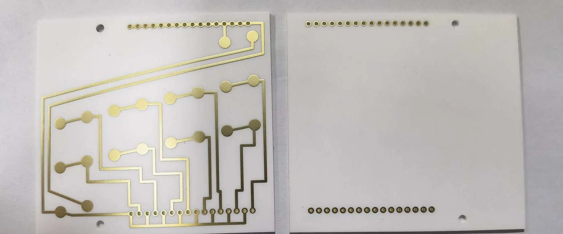
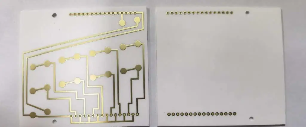
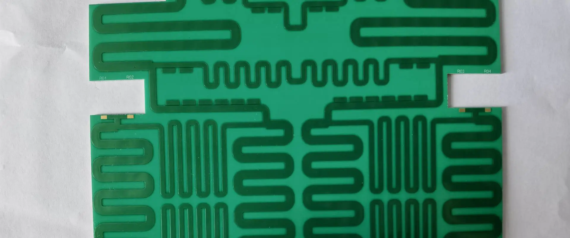
High Tg PCB refers to a printed circuit board manufactured using materials with a high glass transition temperature (Tg). The glass transition temperature is a critical parameter that indicates the point at which a material transitions from a rigid, glassy state to a more flexible, rubbery state.

In the context of PCBs, a high Tg material maintains its structural integrity and electrical properties at elevated temperatures, making it ideal for applications where standard PCB materials would fail. These boards are engineered to withstand higher operating temperatures without compromising performance or reliability.

๐Ÿ”ง RayPCB High TG PCB Engineering Tool
Professional Design Assistant for High Temperature Glass Transition PCBs
๐ŸŽฏ Find Your Ideal TG Level
๐Ÿ“ˆ TG Level Comparison Chart
TG Level Temp Range Cost Factor Best For Lead-Free
Standard (Tg130-140) โ‰ค85ยฐC 1.0x Consumer electronics, Low-cost โš ๏ธ Limited
Medium (Tg150-170) 85-125ยฐC 1.1-1.2x Automotive, Industrial, LED โœ… Good
High (Tg170-180) 125-150ยฐC 1.2-1.4x Server, Telecom, Multi-layer โœ… Excellent
Very High (Tg180-210) 150-175ยฐC 1.5-1.8x Aerospace, Medical, Power โœ… Excellent
Ultra High (Tg250-300+) >175ยฐC 2.5-4.0x Extreme environments, Defense โœ… Superior
Need expert assistance with your High TG PCB project?
Get Instant Quote from RayPCB
ยฉ RayPCB Engineering Tools | Professional PCB Manufacturing Solutions

Properties of High Tg PCB

High Tg PCBs possess several unique properties that set them apart from standard PCB materials:

  1. Thermal Stability: High Tg PCBs maintain their mechanical and electrical properties at elevated temperatures, resisting deformation and degradation.
  2. Low Thermal Expansion: These materials typically have a lower coefficient of thermal expansion (CTE), reducing stress on components and solder joints during temperature fluctuations.
  3. Improved Dimensional Stability: High Tg materials exhibit less warpage and shrinkage, crucial for maintaining precise tolerances in complex multi-layer boards.
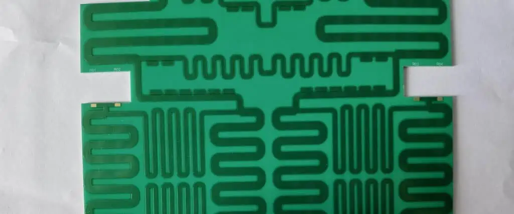
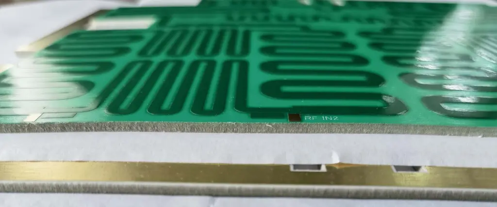
  4. Enhanced Electrical Properties: Many High Tg materials offer superior electrical characteristics, including lower dielectric constants and loss tangents, beneficial for high-frequency applications.
  5. Moisture Resistance: High Tg PCBs often demonstrate better resistance to moisture absorption, reducing the risk of delamination and electrical failures in humid environments.

Advantages of High Tg PCB

Different High Tg PCB Material and its Applications

The unique properties of High Tg PCBs translate into several significant advantages:

  1. Increased Reliability: By maintaining stability at higher temperatures, High Tg PCBs offer improved long-term reliability, especially in harsh environments.
  2. Enhanced Performance: The superior electrical properties of High Tg materials contribute to better signal integrity and reduced signal loss, particularly at high frequencies.
  3. Wider Operating Temperature Range: High Tg PCBs can function effectively in environments where standard PCBs would fail, expanding the potential applications for electronic devices.
  4. Improved Manufacturability: The dimensional stability of High Tg materials allows for more precise manufacturing processes, potentially improving yields in complex PCB designs.
  5. Longer Lifespan: The resistance to thermal degradation and moisture absorption contributes to a longer operational life for electronic devices using High Tg PCBs.

Read more about:

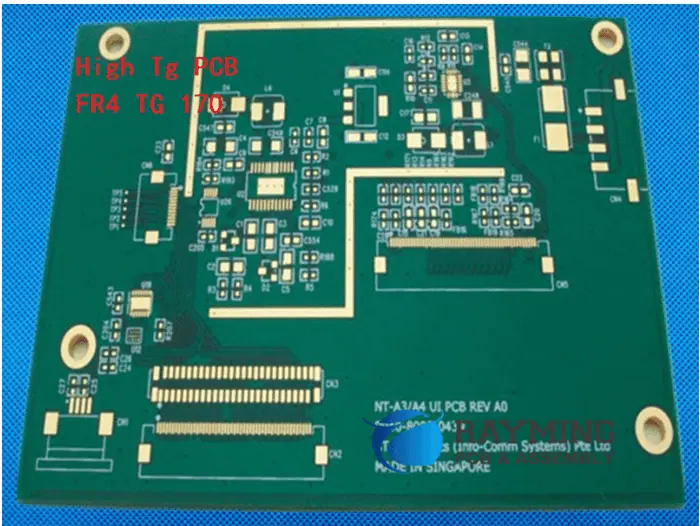
Typical Tg Values for Standard FR-4

Before delving into High Tg materials, it’s important to understand the baseline. Standard FR-4, the most common PCB material, typically has a Tg value ranging from 130ยฐC to 140ยฐC. This serves as a reference point for categorizing higher Tg materials.

Types of Tg Temperature

PCB materials are often categorized based on their Tg values. Here’s a breakdown of common Tg classifications:

1. General Tg (Tg135โ„ƒ)

This category includes standard FR-4 materials, suitable for most consumer electronics and general-purpose applications.

2. Medium Tg (Tg150โ„ƒ)

Slightly higher than standard FR-4, these materials offer improved thermal performance for more demanding applications.

3. High Tg:

The High Tg category encompasses several sub-categories, each offering progressively higher temperature resistance:

3.1 Tg 170

Materials in this range provide a significant step up from standard FR-4, suitable for automotive and industrial applications.

3.2 TG180

Offering even greater thermal stability, TG180 materials are often used in telecommunications and high-reliability consumer electronics.

3.3 Tg200

These materials provide excellent thermal performance, making them suitable for aerospace and advanced industrial applications.

3.4 TG260

With exceptionally high thermal resistance, TG260 materials are used in extreme environments and high-power electronics.

3.5 TG300

At the top end of commercially available PCB materials, TG300 offers unparalleled thermal stability for the most demanding applications.

Material Classification of High Tg

Several types of materials are used to achieve high Tg values in PCBs. Each has its unique properties and advantages:

1. Polyimide (PI)

  • Properties: Extremely high Tg (>250ยฐC), excellent chemical resistance, low outgassing
  • Applications: Aerospace, military, high-temperature industrial environments

2. BT (Bismaleimide Triazine) Epoxy

  • Properties: High Tg (180-220ยฐC), low dielectric constant, low moisture absorption
  • Applications: Telecommunications, high-speed digital circuits

3. PPO (Polyphenylene Oxide)

  • Properties: High Tg (175-220ยฐC), excellent dimensional stability, low dielectric constant
  • Applications: High-frequency RF applications, aerospace

4. LCP (Liquid Crystal Polymer)

  • Properties: Very high Tg (>280ยฐC), extremely low moisture absorption, excellent chemical resistance
  • Applications: High-frequency applications, harsh environment electronics

5. PTFE (Teflon)

  • Properties: High Tg (>250ยฐC), extremely low dielectric constant and loss tangent
  • Applications: High-frequency and microwave circuits, space applications

6. Ceramic Filled PTFE

  • Properties: High Tg (>250ยฐC), improved dimensional stability over pure PTFE, low dielectric constant
  • Applications: High-frequency RF and microwave applications requiring improved thermal management

7. Hydrocarbon Ceramic

  • Properties: High Tg (>200ยฐC), low dielectric constant, excellent dimensional stability
  • Applications: High-speed digital circuits, RF and microwave applications

The Materials RayMing Use for High Temperature PCBs

RayMing, a prominent PCB manufacturer, offers a range of High Tg materials to meet diverse application needs:

1. S1141 (FR4)

  • Tg: 150ยฐC
  • Applications: General-purpose high-temperature applications

2. S1000-2M (FR4)

  • Tg: 170ยฐC
  • Applications: Automotive, industrial control systems

3. S1170G

  • Tg: 180ยฐC
  • Applications: Telecommunications, high-reliability consumer electronics

4. IT180A

  • Tg: 180ยฐC
  • Applications: Automotive, aerospace, high-performance computing

5. Rogers 4350B

  • Tg: 280ยฐC
  • Applications: High-frequency RF and microwave circuits

6. RO4003C

  • Tg: >280ยฐC
  • Applications: High-frequency and high-speed digital applications

7. Isola 370HR

  • Tg: 180ยฐC
  • Applications: Multilayer PCBs for high-reliability applications

8. Isola 406

  • Tg: 170ยฐC
  • Applications: High-layer count PCBs for telecommunications and networking

9. Ventec VT47

  • Tg: 200ยฐC
  • Applications: High-temperature industrial and automotive applications

10. Panasonic R1755V/R1650V

  • Tg: 180ยฐC
  • Applications: High-speed digital circuits, server and network equipment

11. Kingboard KB6167

  • Tg: 170ยฐC
  • Applications: Automotive electronics, industrial control systems

12. Nelco: N4000-6

  • Tg: 170ยฐC
  • Applications: High-speed digital and RF applications

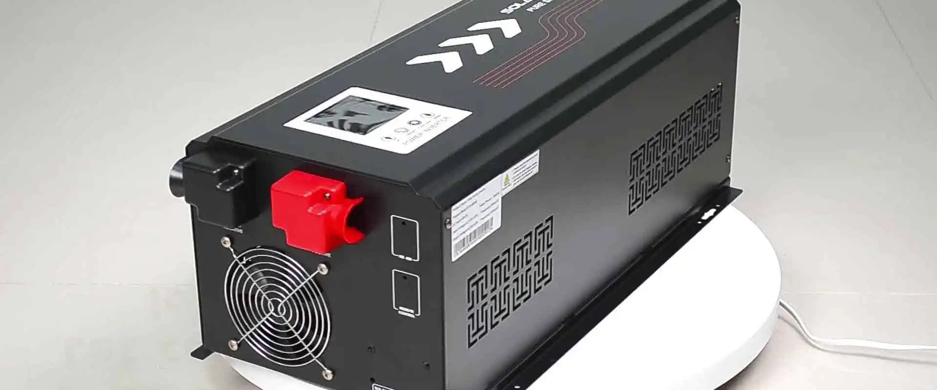
When Do You Need a High Temperature Circuit Board?

High Temperature PCBs become essential in several scenarios:

  1. Extreme Environmental Conditions: Applications exposed to high ambient temperatures, such as automotive under-hood electronics or industrial furnace controls.
  2. High-Power Applications: Circuits dealing with high current or power dissipation, where self-heating is a concern.
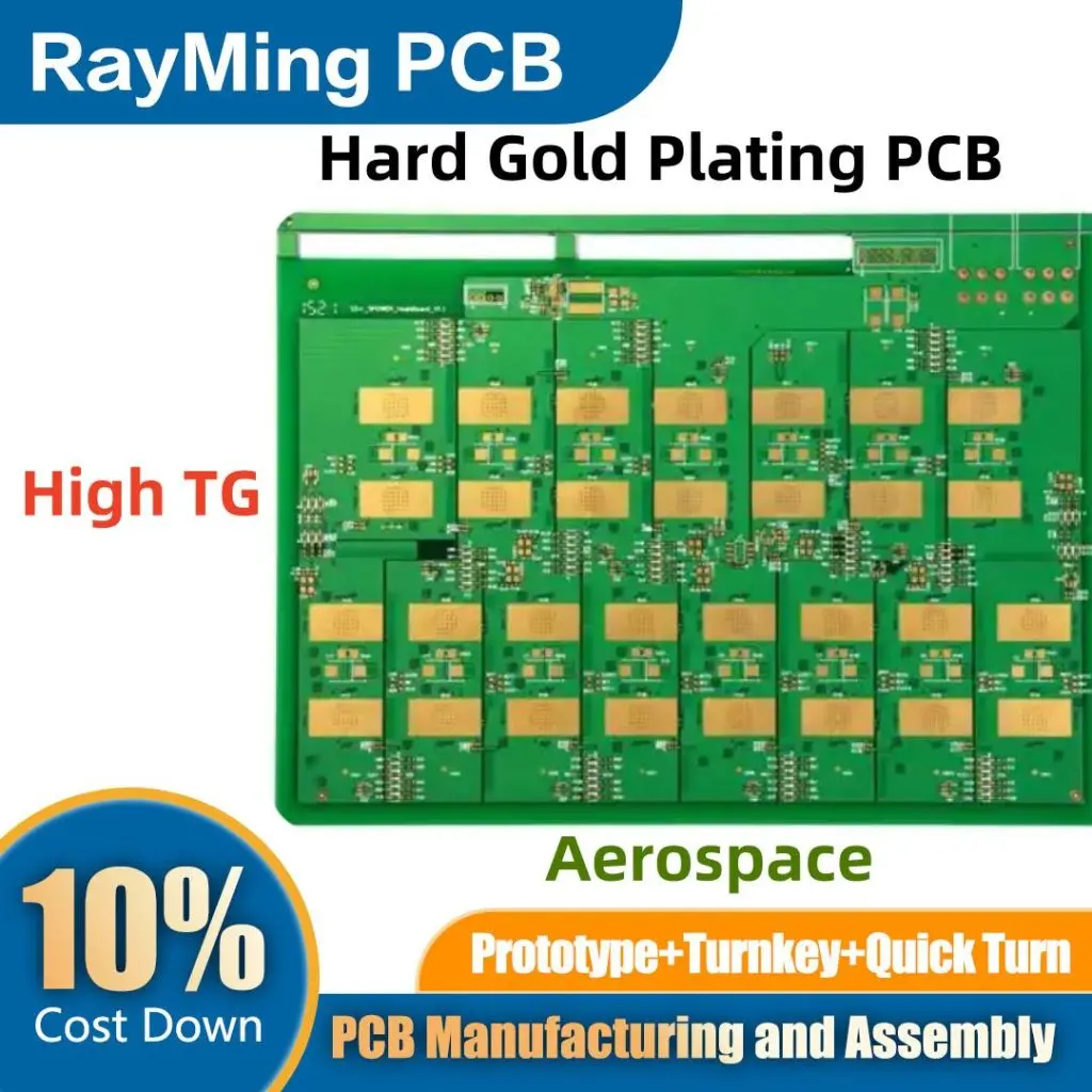
  3. Aerospace and Defense: Applications in aircraft, satellites, or military equipment where reliability under extreme conditions is critical.
  4. Telecommunications Infrastructure: Base stations and network equipment operating in varying environmental conditions.
  5. Oil and Gas Industry: Downhole tools and surface equipment exposed to high temperatures.
  6. LED Lighting: High-power LED applications where thermal management is crucial.
  7. Medical Devices: Certain medical equipment, especially those requiring sterilization at high temperatures.
  8. High-Frequency RF and Microwave Circuits: Applications where maintaining stable electrical properties at high frequencies is essential.

What Is the Difference Between Tg and Td PCB?

While Tg (Glass Transition Temperature) and Td (Decomposition Temperature) are both important thermal parameters for PCB materials, they refer to different aspects of thermal behavior:

  • Tg (Glass Transition Temperature): The temperature at which the material transitions from a rigid, glassy state to a more flexible, rubbery state. This is typically the point where the material begins to soften and lose its dimensional stability.
  • Td (Decomposition Temperature): The temperature at which the material begins to break down chemically, often releasing gases and degrading irreversibly. Td is typically much higher than Tg.

Understanding both Tg and Td is crucial for selecting the appropriate PCB material for a given application:

  • Tg is more relevant for maintaining dimensional stability and mechanical properties during normal operation and manufacturing processes.
  • Td becomes important in extreme conditions or during brief excursions to very high temperatures, such as during soldering or in fault conditions.

Industrial Use of High-Tg PCBs

High-Tg PCBs find applications across a wide range of industries, each leveraging the unique properties of these materials:

  1. Automotive Industry
    • Engine control units
    • Transmission control modules
    • Battery management systems in electric vehicles
  2. Aerospace and Defense
    • Avionics systems
    • Satellite communications equipment
    • Radar and electronic warfare systems
  3. Telecommunications
    • 5G infrastructure equipment
    • High-speed routers and switches
    • Base station amplifiers
  4. Industrial Automation
    • Programmable logic controllers (PLCs)
    • Motor drives and controls
    • Industrial sensors and data acquisition systems
  5. Medical Electronics
    • MRI and CT scan equipment
    • Surgical robots
    • Sterilizable medical devices
  6. Consumer Electronics
    • High-performance gaming consoles
    • 4K and 8K television circuitry
    • High-end audio equipment
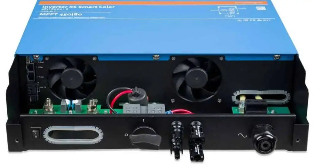
  7. Energy Sector
    • Solar inverters
    • Wind turbine control systems
    • Power distribution equipment
  8. Research and Development
    • Particle accelerators
    • High-energy physics experiments
    • Advanced computing and data centers

Conclusion

High Tg PCBs represent a critical advancement in printed circuit board technology, enabling electronic devices to operate reliably in increasingly demanding environments. From the scorching temperatures under a car hood to the unforgiving vacuum of space, High Tg PCBs are pushing the boundaries of what’s possible in electronic design.

As technology continues to evolve, with devices becoming more powerful and operating in more extreme conditions, the importance of High Tg PCBs is only set to grow. Engineers and designers must carefully consider the thermal requirements of their applications and choose the appropriate High Tg material to ensure optimal performance, reliability, and longevity of their electronic systems.

By understanding the properties, advantages, and applications of High Tg PCBs, professionals in the electronics industry can make informed decisions, driving innovation and enabling the next generation of high-performance electronic devices. Whether it’s in the pursuit of faster telecommunications, more efficient energy systems, or groundbreaking medical technologies, High Tg PCBs will continue to play a crucial role in shaping our technological future.

What is a Raspberry Pi used for?

Raspberry Pi Zero Board

Introduction

The Raspberry Pi is a series of small, affordable single-board computers developed by the Raspberry Pi Foundation. Since launching in 2012, the Pi has become wildly popular among students, hobbyists, hackers, and professionals alike.

But what exactly is the Raspberry Pi capable of? What are some common applications and use cases for this tiny PC? In this comprehensive guide, we’ll explore:

  • Overview of the Raspberry Pi models
  • Key technical specs and capabilities
  • Common Raspberry Pi operating systems
  • Programming options and supported languages
  • Example uses and projects
    • Media center / Retro gaming
    • Networked storage
    • Web server
    • Home automation
    • IoT and sensors
    • Education and learning
    • And many more!
  • Accessories and add-on boards to extend functionality
  • Limitations and downsides of the Pi platform
  • FAQs from the Raspberry Pi community

After reading this detailed article, you’ll have a solid understanding of the many possibilities and uses for the amazingly versatile Raspberry Pi. Let’s get started!

Overview of Raspberry Pi Models

Since the original Raspberry Pi in 2012, newer upgraded models have been released. Let’s briefly cover the different versions available:

Raspberry Pi 1 – The OG Pi released in 2012 with a 700MHz single-core ARM CPU and 256MB RAM. Very basic by today’s standards.

Raspberry Pi 2 – Upgraded Pi released 2015 with a 900MHz quad-core ARM Cortex-A7 CPU and 1GB RAM.

Raspberry Pi 3 – 2016 model with a 1.2GHz 64-bit quad-core ARM Cortex-A53 CPU and 1GB RAM. Added WiFi and Bluetooth.

Raspberry Pi 3 B+ – 2018 revision of Pi 3 with a 1.4GHz CPU, Bluetooth 4.2, and faster Ethernet.

Raspberry Pi 4 – Big upgrade in 2019 to a 1.5GHz quad-core Cortex-A72 CPU, options for 1GB-8GB RAM, USB 3.0, dual monitor support via micro HDMI. Huge leap in performance.

Raspberry Pi 400 – All-in-one Pi integrated into a compact keyboard launched in 2020. Based on Pi 4 compute module.

Raspberry Pi Zero/Zero W – Tiny and ultra low cost Pi models from 2015-2017 with a 1GHz single-core CPU and 512MB RAM.

There are also variants like the Compute Module and industrial models. But this covers the major mainstream Raspberry Pi boards. The Pi 4 provides the most powerful and versatile experience currently.

Now let’s look at some key specs that enable all the Pi’s capabilities.

Raspberry Pi Specifications and Capabilities

Here are some of the most important technical capabilities of the Raspberry Pi hardware and platform:

  • CPU: Modern quad-core ARM processors around 1.5GHz, capable of 32-bit and 64-bit operation. Provides good overall performance for a low-cost board.
  • RAM: 1GB to 8GB LPDDR4 RAM on Pi 4. Important for running desktop OSes and applications.
  • GPU: Powerful integrated graphics supports 1080p video encoding/decoding, OpenGL ES, and flexible display output.
  • Video Output: Dual micro HDMI ports support up to 4Kp60 resolution. Composite video and DSI display outputs also available.
  • Audio: Stereo audio over HDMI or via 3.5mm headphone jack.
  • Networking: Gigabit Ethernet, 802.11ac WiFi, Bluetooth support.
  • USB: 4x USB 2.0 ports, 2x USB 3.0 ports on Pi 4 for ample peripheral connectivity.
  • Storage: MicroSD card slot for loading OSes and storing data.
  • GPIO Pins: 40 flexible GPIO pins to interface with electronics projects.
  • Camera/Display Ports: Integrated camera and display interfaces make it easy to add those modules.
  • Peripherals: Optional hardware like official 7″ touchscreen, case fans and more available.
  • Operating Systems: Can run various Linux distros, Windows 10 IoT, Android Things, and more.
  • Programming: Support for Python, Scratch, C/C++, Node.js, Bash, and many other languages.

This combination of capabilities makes the Pi extremely well-suited for a wide range of applications, as we’ll now explore.

Common Raspberry Pi Operating Systems

One strength of the Raspberry Pi is the ability to run different operating systems based on your needs. Here are some of the most popular OS choices:

Raspberry Pi OS (formerly Raspbian) – The official Debian-based Linux distribution. Recommended starting point.

Ubuntu – Popular Linux distro with desktop and server builds for Pi. Great support.

Windows 10 IoT – Run Windows 10 on your Pi for familiar development environment.

RetroPie – Distro focused on retro gaming emulation. Good for entertainment center builds.

OSMC – Media center focused Linux OS to transform your Pi into a streaming box.

Lakka – Another Linux retro gaming distro similar to RetroPie.

Android Things – Stripped down Android OS from Google for IoT applications.

Twister OS – Raspberry Pi OS fork adding optimizations and additional software.

Manjaro ARM – Arch Linux-based distro designed to be fast and efficient on the Pi 4.

There are also specialty distributions for privacy-focused routing, media playback, enterprise applications, and more. The flexibility to choose different operating systems helps enable different use cases. Now let’s look at programming options.

Programming Languages and Platforms

Raspberry Pi 4
Raspberry Pi 4

The Raspberry Pi supports many programming languages and environments for building software applications and scripts:

Python – Very popular high-level language with huge ecosystem of Pi-focused libraries. Often the first choice.

Node.js – For creating network applications and web servers using JavaScript runtime.

C/C++ – Low level languages with access to hardware capabilities and high performance.

Java – Robust general purpose language well supported on the Pi.

Go – Compiled language gaining popularity for systems programming on Raspberry Pi.

Bash – Standard shell scripting language on Linux to automate tasks and access system functions.

.NET Core/.NET 5 – Run .NET apps with C# or Visual Basic using latest .NET runtime.

Scratch – Graphical programming environment designed to teach kids coding basics.

With this diverse range of supported languages, developers can build virtually any type of application on the Pi. Combined with GPIO pin access, USB ports, onboard video/audio, and accessories, the possibilities are endless!

Next let’s look at some of the most common ways people are using the amazingly versatile Raspberry Pi.

Media Center / Retro Gaming

One of the most popular uses for the Pi is creating customized home entertainment and retro gaming rigs. Its HDMI output, graphics capabilities, and GPIO pin access make it perfect for building your own media center.

You can install RetroPie, Lakka, or other distros to easily emulate games from classic systems like Nintendo, PlayStation, arcades, and more. Pair it with controllers, gaming buttons, a case, and TV connection for an all-in-one retro gaming machine.

For streaming media playback, OSMC is a great choice optimized for the Pi hardware with easy Kodi integration. Network your media files and play them easily.

With a compact form factor, cool case options, and near-silent operation the Pi makes for a slick living room addition for gaming and watching movies.

Networked Storage / File Server

The Raspberry Pi is often used as an inexpensive network attached storage (NAS) device or local file server. This takes advantage of the Ethernet/WiFi connectivity and microSD storage to share files on your network.

Using Samba and/or NFS allows easy mounting of the Pi’s storage from Windows, Mac, Linux machines. SSH provides secure remote shell access for easy administration.

You can also attach external USB drives for increased capacity. For more performance sensitive applications, you can boot the OS from USB 3.0 flash storage.

Overall, the Pi makes accessing shared storage and files simple and cost effective.

Web Server

With its wired and wireless network connectivity, the Pi also functions great as a web server using platforms like Nginx, Apache, Node.js, and more.

Developers can easily host websites and web apps on the Pi to experiment, learn about server administration, and conveniently access the content locally.

For production web serving, the Pi has limitations in performance and reliability versus a true server. But for personal and learning purposes, the Pi’s accessibility makes web hosting and server side development fun and practical.

Home Automation

Another common use case is home automation and IoT. The Pi’s GPIO pins allow easy interfacing with sensors, electronic components, and control systems.

Home Assistant is a popular open source automation platform with great Pi support. It allows monitoring sensors like temperature, controlling devices like lights and motors, automating routines, receiving notifications and more.

You can build one or more Pis into an automation hub to manage your smart home. The wireless and wired connectivity let the Pi communicate with various devices and cloud platforms.

IoT and Sensor Data Logging

Raspberry Pi 3A+
Raspberry Pi 3A+

For industrial IoT applications, the Pi works well at the edge capturing sensor data and interfacing with machinery.

It can connect to PLCs, analog sensors, serial devices, relays, motors, and digital logic easily using the GPIO pins. The Pi then logs data locally, pre-processes it, and transmits upstream.

The compact design also allows placing Pi’s with sensors in tight mechanical installations close to the monitored equipment.

Overall, the Raspberry Pi simplifies adding smarts and connectivity to industrial environments cost effectively.

Education and Learning

Education is a core part of the Raspberry Pi Foundation’s mission. The Pi has been transformational for teaching computing and IT skills to students of all ages.

Its hands-on nature, visual programming options like Scratch, and all-in-one design allows easily grasping electronics and programming basics. Lesson plans using the Pi are widely available.

Computing courses at schools and universities also use the Pi to teach operating system design, networking, security, and of course hardware interfacing skills.

It’s an affordable platform for computer science education and project-based learning. Students also learn Linux administration and practical troubleshooting skills using the Pi.

Robotics

The Pi provides an excellent integrated platform for robotics projects. Its small form factor suits mounting on mobile robots, drones, and robotic arms.

The GPIO pins allow interfacing with motors, servos, and sensors for automation and data capture. The quad-core processor can handle image processing and computer vision algorithms.

Popular robotics frameworks like OpenCV, TensorFlow, and Robot Operating System (ROS) all support the Pi. So developers have access to powerful libraries.

Affordable, packed with capability, and easy to mount, it’s no surprise the Pi has become ubiquitous in the DIY robot builder scene.

Arcade Cabinet

Retro gaming is so popular on the Pi that people build entire arcade cabinet rigs around it. By pairing the Pi with arcade controls, push buttons, an LCD panel in a customized cabinet, you can recreate the entire arcade experience at home.

Install RetroPie or a similar OS, add ROMs for all your favorite classic arcade games, and build an authentic looking cabinet for the full effect. It’s a fun electronics and woodworking project!

The Pi adequately powers even console systems like Nintendo 64 or PlayStation 1 for faithful on-screen gameplay. You can make it as elaborate as you like with marquees, artwork, speakers, etc. A weekend project that turns into a gaming masterpiece.

Security Camera

Leveraging the Pi camera module, you can construct a security camera or surveillance system. Simply add a camera to your Pi, configure streaming and recording software, and place it anywhere that needs monitoring.

MotionEyeOS or the official Pi OS work well out of the box for security camera use. You can also broadcast the stream over the network, record it to shared storage, or save locally on each Pi’s SD card.

The Pi camera supports night vision and higher resolution lenses for capturing detail. Overall, it provides an affordable yet capable backbone for a scalable multi-cam system.

VPN Server / Router

The Pi can serve as a cost effective, low power VPN server using implementations like OpenVPN or Wireguard. This allows securely accessing your home network remotely or tunneling traffic while on insecure public networks.

It’s also handy for running a Pi-hole ad blocking DNS server and Pi VPN server on the same device for privacy protection and removing ads anywhere.

For travel routers, Pi-based devices are compact yet powerful for sharing hotel and vacation rental internet connections securely with all your devices.

So the Pi pulls double duty well as a tiny private VPN server or travel router.

Weather Station

Building your own weather station is straightforward and fun with the Raspberry Pi. Various sensors can be added to collect temperature, pressure, rainfall, wind speed, lightning detection, and more.

The Pi gathers data from all the sensors and can push it upstream to weather services or your own database. It can also drive local dashboard displays to show current conditions.

Sense HAT add-ons make collecting sensor data like environmental readings very easy. The Pi easily creates a full-featured backyard weather monitor.

Smart Mirror

A smart mirror powered by a Raspberry Pi hidden behind a two-way mirror is a creative IoT project. Using a touchscreen lets you interact with the mirror to view news, weather, calendars, todo lists and more.

It provides a central smart home dashboard and easy access to information for your day in an innovative way. Voice control can also be added for hands-free interaction.

While fun to build, it’s also practical as an informational hub mounted in your bathroom, bedroom, or kitchen. A fully-customized smart home assistant designed just how you want.

Cluster Computing

The affordability of the Pi allows forming surprisingly powerful clusters with dozens or even hundreds of nodes. These provide low cost access to high levels of parallel computing power.

Clusters of Raspberry Pis are great for learning about distributed computing while also serving real workloads for research, universities, and hobbyist experimentation.

Kubernetes and Docker Swarm can orchestrate containers across a Pi cluster to run microservice-based applications. With LEGO cases and network wiring, you can build supercomputing-like setups on your desk.

Pi Laptop

For the ultimate portable Pi experience, one popular project is creating a Raspberry Pi laptop. This transforms your Pi into a custom mobile computer.

By integrating a display, battery pack, keyboard, and other peripherals into a case, you can make a Pi-powered laptop. Some kits are even available.

It makes for a fun electronics project while resulting in a practical portable device. With 8GB RAM, the Pi 4 has enough memory to run main desktop OSes like Raspberry Pi OS for a proper laptop experience.

The options and versatility of the Pi enable all kinds of creative computing projects like this.

Accessories and Add-Ons

The Pi foundation and third parties offer various official and unofficial accessories to expand the capabilities of the Pi in your projects:

  • Official 7″ Touchscreen – Fully integrated monitor with touch support.
  • Sense HAT – Board with sensors and 8×8 LED matrix.
  • Camera Modules – Official 5MP and 8MP camera units for photos/video.
  • Pibow Cases – Unique multi-color 3D printed enclosures.
  • Pimoroni – Wide range of fun add-ons like light strips, audio cards, sensors, and more.
  • PiJuice – Uninterruptible power module for continual operation during outages.
  • Snap360 – Camera mount for capturing 360 degree photo spheres.
  • Fan SHIM – Integrated fan with programmable speed control.

The ecosystem of add-ons help tailor your Pi precisely for specialized applications. The sky’s the limit!

Limitations of the Raspberry Pi Platform

While remarkably capable, the Pi does have some limitations to keep in mind:

  • Performance – Can struggle with heavy multimedia workloads sometimes. Not a powerhouse.
  • Memory – 1GB base RAM on older Pis is quite constrained. 8GB on Pi 4 helps tremendously.
  • Storage – booting from microSD cards is slow. USB SSD helps, but not as fast as laptop drives.
  • Peripherals – Limited USB ports makes connecting lots of accessories difficult. Hubs help.
  • Power – Maximizing capabilities draws more electrical power. Careful component selection required.
  • OS Support – Some newer operating systems no longer maintain older Pi compatibility.

So while extremely versatile, the Pi cannot fully replace a high-end PC workstation or server for intensive tasks. But it covers 80% of use cases remarkably well!

Frequently Asked Questions

Here are some common questions that arise when using the Raspberry Pi:

Q: Does the Raspberry Pi replace an Arduino or other microcontrollers?

A: The Pi is like an Arduino on steroids – more powerful CPU and OS, but lacks the precise timing and analog inputs of an MCU. The two are complementary depending on your specific needs.

Q: How difficult is the Raspberry Pi for kids to learn on?

A: Thanks to kid-friendly environments like Scratch and Python, the Pi is quite accessible for introducing children to programming. But may still require parental guidance below age 10.

Q: Which model Raspberry Pi should I get as a starter option?

A: The newer Raspberry Pi 4 Model B with 4GB RAM provides the best overall experience balancing cost, performance, and longevity. Avoid older models like the Pi 1 or Zero.

Q: Is overclocking the Raspberry Pi recommended for extra performance?

A: Overclocking is possible through config tweaks, but be careful! It voids your warranty and puts stability at risk. Modest overclocks may work but expect crashes if pushed too far.

Lead Free Solder Vs Lead Soldering: How to Choose in Electronics Use

Solder is an essential material used in electronics manufacturing to create mechanical and electrical connections between components and printed circuit boards (PCBs). Traditionally solder contained lead, but environmental concerns have driven wide adoption of lead-free solder alloys. However, lead solder still offers some advantages over lead-free alternatives in certain applications. This article compares properties, strengths and limitations of leaded and lead-free solders to help select the optimal type.

Overview of Lead and Lead-Free Solders

Solder is a metal alloy that liquifies at relatively low temperatures making it ideal for electronics assembly. It flows into the joint, then solidifies forming permanent electrical and mechanical soldered connections. Here is a brief overview comparing traditional lead solder versus modern lead-free solder:

Lead Solder

  • Contains 30-40% lead alloyed with tin
  • Melting point around 180-190ยฐC
  • Excellent wetting and flow characteristics
  • Relatively low cost
  • Toxic – restricted in some regions

Lead-Free Solder

  • Replaces lead with silver, copper, bismuth etc.
  • Higher melting point, typically 217-220ยฐC
  • More difficult wetting and flow
  • Higher cost than leaded
  • Reduced environmental impact

Both offer trade-offs that make each preferable for certain applications as we will examine in detail.

Why Choose Lead-Free Solder?

Lead-free solder alloys eliminate toxic lead to mitigate environmental and health hazards associated with electronics waste:

Reduced Environmental Contamination

  • Lead persits indefinitely and accumulates in the environment when electronics are improperly discarded in landfills. Lead-free solder reduces lead contamination risks.

Improved Worker Safety

  • Lead exposure negatively impacts personnel health. Lead-free solder helps protect assembly line staff from lead’s neurological and reproductive toxicity when handled regularly.

Complying With Regulations

  • Laws like the Restriction of Hazardous Substances (RoHS) directive ban lead solder from consumer electronics to reduce lead waste pollution. Most electronics OEMs have transitioned to comply.

Avoiding Lead Contamination

  • Lead can contaminate food processing equipment and medical devices leading to health risks. Lead-free solder prevents lead leaching.

Minimizing Disposal/Recycling Issues

  • Separating and properly recycling leaded waste adds cost. Lead-free products simplify end-of-life disposition.

For most new consumer product designs, lead-free solder is now standard. But in specialized cases, leaded solder still offers advantages.

Why Lead Solder Remains Advantageous

Despite the push towards lead-free electronics, leaded solder provides some ongoing benefits in certain applications:

Lower Melting Point

  • Lead solder melts around 180-190ยฐC versus 210-220ยฐC for lead-free. This allows use with heat sensitive components.

Improved Wetting and Flow

  • Lead alloys readily wet and spread on copper and component leads. Lead-free solder can require flux assistance.

Reduced Joint Cold Flow Stress

  • Softer lead solder reduces shear stresses on thermal cycle. Lead-free joints more prone to tin whiskering.

Lower Cost

  • The continued wide availability of tin-lead solder keeps costs modest. Some lead-free alloys utilize expensive metals.

Exemption for Defense/Aerospace

  • Mission critical military and avionics applications still permit lead due to reliability concerns.

Repairability

  • Leaded solder joints are easier to reheat for component replacement versus lead-free.

Lead solder remains preferable for many high reliability industrial, military, aerospace, and maintenance applications where its unique advantages outweigh toxicity concerns.

Lead-Free Solder Alloys

Lead-free solders most often consist of tin alloyed with metals like silver, copper and bismuth to mimic lead’s properties as closely as possible. Common compositions include:

SnAgCu (SAC) โ€“ Tin-Silver-Copper (95.5Sn/3.9Ag/0.6Cu)

  • Most popular lead-free alloy
  • Good mechanical properties
  • Prone to tin whiskering

SnCu โ€“ Tin-Copper (99Sn/0.7Cu)

  • High tin content improves ductility
  • High melting point of 227ยฐC

SnAg โ€“ Tin-Silver (96.5Sn/3.5Ag)

  • Contains costly silver
  • Susceptible to silver leaching

SnBi โ€“ Tin-Bismuth (42Sn/58Bi)

  • Lowest melting point of just 138ยฐC
  • Brittle with poorer thermal fatigue

SnZn โ€“ Tin-Zinc (91Sn/9Zn)

  • Zinc lowers melting point to 199ยฐC
  • Can corrode and weaken over time

SnAgBi – Tin-Silver-Bismuth

  • Contains silver for strength and bismuth for ductility

Alloy composition balances properties like melting point, joint strength, ductility, thermal fatigue and cost.

Comparison of Lead and Lead-Free Solder Properties

Here is how typical 63/37 tin/lead solder compares to common 95.5/3.9/0.6 Sn/Ag/Cu lead-free solder for key properties:

Property63Sn/37Pb95.5Sn/3.9Ag/0.6Cu
Melting Point183ยฐC217ยฐC
Electrical Conductivity15% IACS12% IACS
Thermal Conductivity35 W/mK60 W/mK
Coefficient of Thermal Expansion29 ppm/ยฐC23 ppm/ยฐC
Yield Strength16 MPa41 MPa
Elongation at Break40%40%
Creep ResistanceExcellentGood
Wetting CharacteristicsExcellentFair

Lead-free alloys compensate for drawbacks like higher melting point and poorer wetting through exact alloy adjustments and flux chemistries.

Mixing Lead and Lead-Free Solder

Ideally all soldering in a given product is done using consistent solder alloy to avoid incompatibility between joints:

  • Mixing leaded and lead-free solders risks formation of brittle intermetallic layers that weaken joints
  • Using lead-free solder over broader temperature profiles risks melting adjacent leaded solder joints
  • Matching solder alloy and flux core is optimal for wetting and flow

For niche cases allowing some mixed soldering, like repairing older electronics, observe these precautions:

  • Keep joint types isolated – leaded for repairs, lead-free for new soldering
  • Ensure the melting point of existing solder is 5-10ยฐC higher than the applied new solder
  • Use solder wick to fully remove previous solder before applying new alloy
  • Swap component leads if feasible to avoid soldering dissimilar alloys to the same leads

It is best practice however to standardize on one solder alloy per product during design when possible.

Lead Solder Application Notes

When working with traditional tin-lead solder:

  • Choose an alloy blend like Sn60/Pb40 or Sn63/Pb37 suited to the thermal needs
  • Specify flux-cored wire or paste for easiest application
  • Use the lowest temperature producing good flow to minimize thermal stress
  • Allow adequate cool down time since leaded solder remains molten longer
  • Employ adequate fume extraction due to lead vapor exposure risks
  • Follow safe lead handling procedures to avoid ingestion or skin contact
  • Properly label any product containing lead for recycling/disposal

With careful handling, lead solder remains an appropriate choice for high reliability industrial electronics not subject to RoHS regulations.

Lead-Free Solder Application Notes

To successfully apply lead-free solders:

  • Select alloy suited to process capabilities, like Sn/Ag/Cu or Sn/Cu
  • Use solder specifically formulated for lead-free use
  • Increase process temperatures to reach higher melting point
  • Adjust dwell times to achieve proper wetting with lead-free alloys
  • Use sufficient flux designed to eliminate lead-free processing issues
  • Review any component specifications for lead-free soldering suitability
  • Follow cleaning processes to remove all lead-free flux residues

With process adjustments, lead-free solders can deliver sufficient joint strength and reliability.

Lead-Free Solder Rework and Repair

Reworking and repairing lead-free solder joints raises challenges:

  • Higher melting point makes removal more difficult
  • Leaded solder should not contact lead-free joints
  • Traces may delaminate if overheated
  • Preheating is essential to minimize thermal shock
  • Flux must be thoroughly cleaned afterwards

Methods to rework lead-free solder connections:

  • Use hot air tool, mini soldering iron, or reflow oven
  • Preferentially heat component and junction, not entire board
  • For BGAs, use hot air nozzle following profile specifications
  • Remove all previous solder first before re-applying fresh solder

With care, lead-free solder joints can be successfully reworked or repaired.

Selecting Lead or Lead-Free Solder

Use lead solder when:

  • High reliability is critical – aerospace, military, automotive
  • Repairability and long service life are needed
  • Heat-sensitive components prohibit higher temperatures
  • RoHS regulations do not apply to the product
  • Process is already optimized for lead solder

Use lead-free solder when:

  • Consumer safety from lead contamination is paramount
  • Adhering to RoHS regulations for commercial products
  • Establishing an environmentally friendly process
  • Heat-resistant components permit higher temperatures
  • New process development allows optimizing for lead-free

Evaluate criteria like temperature limits, reliability, regulation, environmental impact and manufacturability when selecting solder alloy. With attention to detail, both leaded and lead-free solder can produce robust joints.

Summary of Lead vs. Lead-Free Solder Trade-Offs

  • Lead solder offers a lower melting point and superior wetting and ductility but carries toxicity concerns.
  • Lead-free solder eliminates lead risks but requires higher temperatures, precise alloying and well-controlled processes.
  • Each option has benefits making it preferable for particular applications subject to different technical and regulatory constraints.
  • Electronics assemblies should ideally standardize on consistent lead or lead-free solder, not mix alloys.
  • With well-developed processes, both solder alloy families can achieve excellent, reliable solder connections.

Understanding the trade-offs helps designers select the right solder type for each product based on performance, safety, reliability and other requirements.

Frequently Asked Questions

60 40 Vs 63 37 Solder

What are the most widely used lead-free solder alloy compositions?

The most common lead-free solder alloys used in electronics are:

  • SnAgCu (95.5Sn/3.9Ag/0.6Cu)
  • SnCu (99Sn/0.7Cu)
  • SnAg (96.5Sn/3.5Ag)
  • SnBi (42Sn/58Bi) – for very low melting points

Engineers select different ratios based on properties needed like melting point, strength, cost, and manufacturability.

Is lead-free solder always required? Are any exemptions allowed?

Lead solder remains permissible in:

  • Aerospace, military, and high reliability applications
  • Maintenance and repair of existing leaded electronics
  • Certain high temperature electronics
  • Applications exempt from RoHS regulations

If lead contamination is not a concern, leaded solder can still offer advantages.

What can mitigate the higher melting point challenges of lead-free solder?

Methods to conquer lead-free solder’s higher melting point include:

  • Adjusting process temperature settings higher
  • Lengthening dwell times over joints
  • Usingria appropriate soldering iron tip sizes/temps
  • Employing profiling techniques like ramp-soak-spike
  • Selecting alloy compositions with lower melting points
  • Verifying components meet higher temperature needs

With robust process development, reliable lead-free soldering is certainly achievable.

Via Filling in PCB Design: Key Techniques for Reliable Fabrication

A VIA hole in a PCB

PCB via filling is a critical manufacturing technique where plated through-holes are filled with either conductive or non-conductive material. This process enhances circuit board reliability by preventing air or liquid entrapment, reducing the risk of defects in demanding applications.

What is Via Filling?

Via filling is a process used in PCB manufacturing to enhance the reliability and performance of vias – the small holes that connect different layers of a multilayer PCB. These holes are typically plated with conductive material to create electrical connections between layers. However, in some cases, especially in high-density interconnect (HDI) boards or boards subject to harsh environments, simply plating the vias isn’t enough.

Via filling involves completely or partially filling these holes with conductive or non-conductive materials. This process serves several purposes:

  1. Improving thermal management
  2. Enhancing structural integrity
  3. Preventing contamination
  4. Enabling via-in-pad designs
  5. Improving the overall reliability of the PCB

Read more about:

Types of Via Filling

There are two main types of via filling used in PCB manufacturing:

Conductive Polymer Filling

Conductive polymer filling involves using a conductive material, typically a mixture of epoxy resin and conductive particles like copper or silver, to fill the vias. This method maintains the electrical connectivity between layers while providing additional benefits:

  • Enhanced current-carrying capacity
  • Improved thermal management
  • Better mechanical strength

Conductive filling is often used in high-power applications or when via-in-pad design is required.

Non-Conductive Via Plugging

Non-conductive via plugging uses non-conductive epoxy or resin to fill the vias. While this method doesn’t contribute to electrical connectivity, it offers several advantages:

  • Prevents solder from wicking through the via during assembly
  • Improves planarity for surface mount components
  • Enhances the board’s structural integrity
  • Protects against contamination

Non-conductive filling is commonly used in applications where via-in-pad isn’t necessary, but improved reliability and manufacturability are desired.

Cost Considerations for Conductive and Non-Conductive PCB Via Filling

The cost of via filling can vary significantly depending on several factors. Understanding these can help in making informed decisions during the PCB design process.

4 Factors That Affect the Via-Filling Cost

1. Hole Count

The number of vias that need to be filled directly impacts the cost. More holes mean more material and more processing time, leading to higher costs.

2. Type of Paste

The material used for filling affects the cost. Conductive pastes, especially those containing precious metals like silver, are generally more expensive than non-conductive options.

3. Manufacturing Complexity

The complexity of the PCB design, including factors like board thickness, via size, and aspect ratio, can influence the difficulty of the filling process and, consequently, the cost.

4. Testing and Quality Control

Rigorous testing and quality control measures are essential to ensure proper filling and reliability. These additional steps contribute to the overall cost but are crucial for producing high-quality PCBs.

Alternative Budget-Friendly Via-Filling Techniques

For projects with tighter budgets, alternative techniques can be considered:

Advantages of Via Fill Plug with LPI Solder Mask

Liquid Photoimageable (LPI) solder mask can be used to plug vias, offering a cost-effective alternative to traditional filling methods. Advantages include:

  • Lower material costs
  • Simpler manufacturing process
  • Adequate protection for many applications

Disadvantages of the Via Fill Plug with LPI Solder Mask

However, this method has some limitations:

  • Less reliable than traditional filling methods
  • Not suitable for via-in-pad designs
  • May not provide sufficient protection in harsh environments

Reducing Via Fill Costs in High-Volume Productions

For high-volume production, consider these cost-effective techniques:

Via Fill Plug

This method involves partially filling the via with conductive or non-conductive material, then covering it with solder mask. It’s less expensive than complete filling while still providing many benefits.

Plate Shut

For smaller vias, plating the hole until it’s completely closed can be a cost-effective alternative to filling. This method works well for vias with diameters less than 0.3mm.

Fab Notes for Via Filling

When specifying via filling in your PCB design, clear and detailed fabrication notes are crucial. Here are some key points to include:

  1. Specify the type of filling material (conductive or non-conductive)
  2. Indicate which vias need to be filled (all vias, specific sizes, or locations)
  3. Specify the filling method (complete fill, partial fill, or cap plating)
  4. Include any specific requirements for planarity or void percentage
  5. Reference relevant IPC standards

Clear fab notes ensure that your design intent is accurately communicated to the PCB manufacturer, reducing the risk of errors and misunderstandings.

IPC 4761 Standards for Via Filling and Via Covering

The IPC 4761 standard provides guidelines for via protection in PCBs. It defines seven types of via protection:

  1. Type I: Tented (Single Side)
  2. Type II: Tented (Double Side)
  3. Type III: Tented and Covered (Double Side)
  4. Type IV: Plugged
  5. Type V: Plugged and Covered
  6. Type VI: Capped
  7. Type VII: Filled and Capped

Understanding these standards and specifying the appropriate type in your design documentation ensures that your PCB manufacturer follows industry-recognized practices for via protection and filling.

How Do You Fill Vias During PCB Manufacturing?

The via filling process can vary depending on the specific requirements of the PCB design. Here are two common scenarios:

Filling of Via-in-Pad

Via-in-pad designs require complete filling of the via to create a flat surface for component placement. The process typically involves:

  1. Cleaning the via to ensure good adhesion
  2. Injecting conductive or non-conductive paste into the via
  3. Curing the filling material
  4. Planarizing the surface to ensure flatness
  5. Plating over the filled via to create a solderable surface

Filling of Microvias in HDI Boards

Filling microvias in HDI boards requires precision due to their small size. The process often includes:

  1. Carefully controlling the amount of filling material to avoid overfill or underfill
  2. Using specialized equipment designed for microvia filling
  3. Implementing strict quality control measures to ensure complete filling without voids

Via Filling Methods

There are two primary methods used for filling PCB vias:

1. Copper Plating

Additional copper electroplating is used to fill via holes fully with copper after initial plating:

  • Electrolytic process deposits copper inside drilled holes
  • Repeated cycles build up copper thickness
  • Copper grows evenly around barrel walls
  • Continues until via hole is 100% filled

Plating helps ensure uniform copper fill quality and reliable connections. But plating equipment represents a significant capital cost.

2. Conductive Ink Filling

Liquid solder masks or conductive inks are used to fill via interiors:

  • Allows filling vias after drilling
  • Ink injected by dispensing, stencil printing or other deposition
  • Fills multiple vias simultaneously
  • Inks cure when heated after board fabrication

Conductive inks provide a lower cost, more scalable via filling solution. But even ink filling can be challenging without optimized processes.

Now letโ€™s examine popular materials used for filling vias.

Via Filling Materials

Common materials used to fill PCB vias include:

Electroplated Copper

  • Pure copper fills via through electroplating
  • Excellent conductivity (IACS 100%)
  • Readily bonds with copper barrel
  • Reliable, uniform filling results
  • Higher equipment costs

Electroless Copper

  • Auto-catalytic copper deposition
  • Slightly lower conductivity than pure copper
  • Cannot build up thickness as much as electroplating
  • Provides conformal coating over hole walls
  • Lower cost technique

Solder Mask

  • Liquid photoimageable solder mask ink
  • Cures into solid epoxy fill when heated
  • Relatively high resistivity depends on filler metals
  • More prone to voids without process controls
  • Lower cost method

Conductive Epoxy

  • Two-part conductive epoxy adhesives
  • Filled with silver, carbon or nickel particles
  • Moderate conductivity depends on filler type/load
  • Can be dispensed or stencil printed into vias

The optimal via filling material balances electrical, thermal, reliability, and manufacturing cost considerations.

Failure Analysis of Filled Vias

Despite best practices, filled vias can sometimes fail. Understanding common failure modes can help in designing more reliable PCBs:

1. Fractures in the Via Wall Create an Electrical Discontinuity

Thermal stress or mechanical shock can cause fractures in the via wall, leading to open circuits. Proper design considerations, such as using more flexible filling materials or implementing stress-relief features, can mitigate this risk.

2. Voids in Filled Vias Cause Reliability Issues

Air pockets or voids in the filling material can lead to reliability problems. These voids can expand under heat, causing the filling to crack or separate from the via wall. Strict process control and quality inspection are essential to minimize void formation.

3. Environmental Impurities Can Result in Voids

Contamination during the filling process can create voids or weak spots in the filling material. Maintaining a clean manufacturing environment and using high-quality materials are crucial for preventing this issue.

4. An Imbalanced Plating Process Can Cause Voids

In plated vias, an imbalanced plating process can lead to uneven plating thickness or voids. This can compromise the electrical and mechanical integrity of the via. Proper control of plating parameters and regular maintenance of plating equipment are necessary to ensure consistent results.

Conclusion

Via filling is a critical process in PCB manufacturing that significantly impacts the reliability and performance of electronic products. By understanding the types of via filling, cost considerations, manufacturing processes, and potential failure modes, PCB designers and manufacturers can make informed decisions to create high-quality, reliable boards.

Whether you’re working on a high-density interconnect board for a cutting-edge mobile device or a rugged industrial control system, mastering the art of via filling is essential for success in today’s competitive electronics industry. By following industry standards, implementing best practices, and staying informed about the latest techniques, you can ensure that your PCB designs meet the demanding requirements of modern electronic applications.

What is PCB ink?

Introduction

Printed circuit board (PCB) manufacturing relies on depositing and patterning conductive materials to form the traces and features that carry signals and power. The conductive pastes and liquids used to create these circuit patterns are referred to as PCB inks.

PCB inks consist of conductive particles suspended in an adhesive formulation. After deposition and curing, these inks make up the copper circuitry that connects components on a PCB. This article provides an in-depth overview of PCB inks including:

  • Composition and properties of typical PCB inks
  • Different ink types and characteristics
  • PCB fabrication processes utilizing inks
  • New developments in ink formulations
  • Advantages of ink-based circuit fabrication
  • Considerations when selecting and applying inks
  • Examples of practical PCB ink applications

Understanding PCB ink technologies and capabilities allows engineers to consider the optimal materials and processes to fulfill circuit fabrication needs.

Composition of PCB Inks

PCB inks contain two primary constituents:

Metal Particles – Small conductive metal particles, typically copper or silver, make up 50-90% of an inkโ€™s mass. The key properties of the metal particles include:

  • High intrinsic conductivity
  • Purity – oxygen-free highly pure metals
  • Particle shape – spherical, flakes or mixtures
  • Particle size distribution – sub-micron to tens of microns
  • Oxidation resistance – for stable shelf life

Adhesive Matrix – A polymer binder adheres the metal particles together and bonds the cured ink to the substrate. Key properties include:

  • Solvent compatibility – soluble for deposition
  • Cure chemistry – thermal, UV, moisture, catalyst
  • Flexibility – maintains conductivity during bending
  • Adhesion strength – bond to substrates
  • Decomposition temperature – for operating range

The proportions and properties of these two components fundamentally define the performance of a PCB ink. Different ink types make trade-offs between these constituents to achieve specific characteristics.

Types of PCB Inks

There are several varieties of PCB inks formulated for different applications and processes:

Silver Flake Inks

  • High solid loading (60-85%) of silver flakes
  • Low curing temperature
  • Best electrical conductivity but higher cost

Copper Particle Inks

  • Moderate solid loading (50-60%) of copper
  • Low oxidation provides optimal stability
  • Lower cost than silver but higher resistance

Nano Copper Inks

  • Copper nanoparticles under 100nm
  • Enables low-temperature sintering
  • High electrical performance

Nano Silver Inks

  • Extremely fine (<50nm) silver particles
  • Lower curing temperature while maintaining conductivity
  • Printable using inkjet methods

Carbon Inks

  • Small graphite or carbon black particles
  • Lower conductivity than silver/copper
  • Often used for resistive elements

Each ink type exhibits trade-offs between performance, process compatibility, shelf life and cost.

PCB Fabrication Processes Using Inks

PCB inks serve different roles across common fabrication processes:

Printed Electronics

  • Inkjet, aerosol, screen and pad printing all deposit tracks
  • Low-temperature curing forms circuits

Conformal Printed Circuits

  • Inks printed on 3D surface
  • Enable flexible physiques

Flexible Circuits

  • Inks cured on polyimide substrates
  • Withstand bending and flexing

Additive Circuit Formation

  • Inks printed on PCB substrates
  • Add high density interconnects

Selective Plating

  • Ink masking layer defines plating areas
  • Removed after plating

EMI Shielding

  • Conductive inks add shielding to enclosures
  • Protects electronics

Inks provide versatility across diverse PCB manufacturing processes spanning printed electronics to plating to conformal circuits and more.

Advances in PCB Ink Formulations

Ongoing research and development continues expanding PCB ink capabilities through:

Lower Curing Temperature

  • Enables printing on temperature-sensitive substrates
  • Prevents component damage during curing

Finer Particles

  • Reduces required curing temperature
  • Provides higher resolution printing

Hybrid Particle Shapes

  • Tailor viscosity, densification and sintering
  • Optimize printing and electrical characteristics

Graphene Inks

  • Imparts flexibility, thermal conduction
  • Potential for lower costs

Copper and Nickel Inks

  • Alternatives to costly silver inks
  • Nearly matching electrical properties

Biocompatible Inks

Innovation in ink chemistry and materials science unlocks new potential applications.

Considerations When Selecting PCB Inks

Key considerations when choosing a PCB ink include:

Printing Method

  • Inks are formulated specifically for deposition techniques
  • Screen, inkjet, aerosol and other printing

Substrate Material

  • Adhesion strength varies with substrates
  • CTE matching prevents delamination

Curing Requirements

  • Ink curing method must match equipment
  • Temperature, UV, moisture, catalyst

Print Resolution

  • Particle size distribution affects achievable features
  • Finer particles enable smaller printed details

Shelf Life

  • Particle oxidation resistance impacts usable life
  • Refrigeration prolongs life

Operating Environment

  • Temperature, humidity, mechanical stresses
  • Ink must maintain performance across conditions

Properly matched ink, process and substrate produces optimal results.

PCB Ink Application Examples

Here are some examples of practical PCB ink applications:

Flexible Circuits

  • Silver polymer thick film ink printed on polyimide
  • Withstands repeated bending for wearable device

Conformal Antenna

  • Aerosol printed copper ink on curved surface
  • Enables non-planar smart device communication

Automotive Sensors

  • Copper ink printed circuits on polymer housing
  • Integrates PCBs into modules

Medical Patches

  • Biocompatible silver/graphene ink circuits
  • Adheres to skin for health monitoring

EMI Shielding

  • Silver ink applied inside device enclosure
  • Protects electronics from interference

Heater Elements

  • Highly resistive carbon ink printed on glass
  • Provides localized transparent heating

These examples illustrate the diversity of possibilities using printed inks for circuit fabrication.

Frequently Asked Questions

Here are some common questions that arise regarding PCB inks:

Q: What is the main trade-off between silver and copper inks?

Silver inks provide higher conductivity but at a higher raw materials cost, while copper offers a more affordable option with slightly higher resistivity.

Q: What are some methods used to deposit PCB inks?

Common methods include screen printing, inkjet printing, aerosol printing, flexographic printing and syringe dispensing.

Q: How small of circuit features can be produced using PCB inks?

The finest features range from 10-50 microns depending on the printing process resolution, particle sizes, and post-printing curing approach used.

Q: Do PCB ink patterns require plating for most applications?

Often yes, plating improves conductivity and durability. But some applications like embedded heating elements can utilize printed ink-only circuits.

Q: What are the shelf life considerations for PCB inks?

Shelf life varies based on formulation, with silver flake inks lasting 1-3 years refrigerated. Use within 6 months is recommended for optimal results.

Conclusion

PCB inks enable versatile printed circuit fabrication techniques spanning printed electronics, EMI shielding, heaters, sensors, and more. As ink formulations and printing processes continue advancing, ink-based circuit manufacturing empowers new design possibilities and applications. Understanding the composition, types, processes and properties of these conductive inks allows engineers to take full advantage of their capabilities and expand the horizons for PCB innovation.

Which is Better Low Frequency or High-frequency Inverter?

Introduction

Inverters convert DC power into AC power to operate AC equipment and devices. They utilize power electronic switching at different frequencies to generate the AC output. This articles examines low frequency inverters operating near the AC line frequency versus high frequency inverters using much higher switching frequencies. The comparative advantages and disadvantages are analyzed to determine which approach is better suited for different applications.

Defining Low and High Frequency Inverters

Low Frequency Inverters

  • Use switching frequencies close to 50/60Hz line frequency
  • Typically 100 Hz to 5 kHz range
  • Requires large inductors and capacitors

High Frequency Inverters

  • Switch at much higher 10s of kHz to MHz frequencies
  • Very high ratio between switching and output frequency
  • Allows use of smaller filter components

Frequency Ratio

  • Low frequency inverters have ratio of up to 1:100
  • High frequency inverters reach 1:1000 to 1:50,000 ratios

Low Frequency Inverter Operation

[Simple circuit diagram]

  • Full bridge topology commonly used
  • MOSFETs or IGBTs switched at line frequency rates
  • Large AC inductor filters output to smoothen waveform
  • Produces nearly sinusoidal voltage at line frequency

High Frequency Inverter Operation

[Simple circuit diagram]

  • Similar bridge topology used
  • Operates at much higher switching frequency
  • Smaller inductor and capacitor filters the output
  • Generate clean sine wave at desired line frequency

Comparison of Characteristics

ParameterLow Frequency InverterHigh Frequency Inverter
TopologyFull bridge usually usedMost use full bridge
Switching Frequency100 Hz to 5 kHz20 kHz to 1 MHz
Frequency RatioUp to 1:100Up to 1:50,000
Filter SizeLarge inductors and capacitorsSmall inductors and capacitors
SemiconductorsBJTs, MOSFETs, IGBTsMOSFETs, IGBTs
Control ComplexitySimpleComplex high-speed control
EfficiencyModerateVery high
Power DensityLowVery high
DistortionHigher harmonics presentLow harmonic distortion
Response SpeedSlowVery fast
Physical SizeLargeCompact
WeightHeavyLight
ApplicationsUPS, motor drives, PV invertersDrives, UPS, aircraft, medical

Low Frequency Inverter Benefits

Some benefits of low frequency inverters include:

Simplicity

  • Requires only basic controls for switching
  • Open loop voltage control is straightforward
  • Does not need specialized driver circuits

Robustness

  • High overload capacity due to larger components
  • Less affected by noise and temperature variations
  • High reliability and ruggedness

Low EMI

  • Very little high frequency interference generated
  • Minimal filtering needed for EMI compliance

Low Acoustic Noise

  • Any switching noise present at inaudible frequencies
  • Minimal acoustic noise issues

Lower Cost

  • Cost effective magnetic components
  • Simple semiconductor selection
  • Minimal additional circuitry needed

High Frequency Inverter Advantages

Salient advantages of high frequency inverters:

Compact Size

  • Extremely small due to high-frequency magnetics
  • High power density up to 50W/cubic-inch
  • Ideal for lightweight portable applications

Fast Response

  • Very fast transient response speed
  • Precise and agile control ability
  • Well suited for dynamic speed or voltage regulation

High Efficiency

  • Up to 97% efficiency achievable
  • Lower conduction and switching losses
  • Reduces running costs and heat sinking needs

Light Weight

  • Massive reduction in magnetics and filters
  • Superior power-to-weight ratio
  • Easier mounting and portability

Quiet Operation

  • Any audible noise pushed into ultrasonic range
  • Nearly silent operation suitable for occupied spaces

Disadvantages of Low Frequency Inverters

Some drawbacks of low frequency inverters include:

Large Size

  • Significant space needed for large inductors and capacitors
  • Limits applications with space constraints

Slower Response

  • Cannot quickly change output voltage or frequency
  • Not suitable for dynamic speed or voltage control

Distortion

  • May have considerable lower order harmonics
  • Additional filtering required for sensitive loads

Acoustic Noise

  • Audible noise around switching frequency
  • Irritating hum or buzz if in human audible range

Lower Efficiency

  • Hard-switched topology causes increased losses
  • Heat sinking needs add cost and size

Drawbacks of High Frequency Inverters

Some limitations of high frequency inverters:

Complexity

  • Requires sophisticated control methods and ICs
  • Challenging gate drive design for reliable switching
  • Overall system design complexity increased

EMI Issues

  • High frequency switching generates interference
  • Needs substantial EMI filtering

Reliability Concerns

  • Hard switching and thermal cycling degrade reliability
  • Device failure rates may be higher

Acoustic Noise

  • Ultrasonic losses need to be attenuated
  • Can cause issues with adjacent electronic systems

Higher Cost

  • Specialized high-speed devices increase costs
  • Additional circuits add expense
  • May require modular construction

Choosing Between Low and High Frequency Inverters

Low frequency inverters are advantageous for:

  • Simple low cost inverter designs
  • High reliability requirements
  • High overload capacity needed
  • Situations where EMI is detrimental
  • Applications with audible noise constraints

High frequency inverters are better for:

  • Very compact portable systems
  • Weight critical applications like aerospace
  • High precision fast response speed needed
  • High efficiency essential to reduce losses
  • Meeting tight harmonic distortion requirements

Conclusion

  1. Low frequency inverters are simpler, more robust and easier to control.
  2. High frequency inverters enable miniaturization, fast response, efficiency and ultra-quiet operation.
  3. The choice depends on the specific size, performance, cost, reliability and noise criteria for the application.
  4. Hybrid inverters running at medium frequencies can balance the tradeoffs.
  5. Advances in topology, modulation, devices and materials continue to improve low and high frequency inverter performance.

Frequently Asked Questions

What is the typical frequency range considered as “high frequency” for inverters?

Inverters operating from around 10 kHz up to 1 MHz are considered high frequency, compared to low frequency inverters running under 5 kHz.

What are the main advantages of low frequency inverters?

Simplicity, ruggedness, low EMI, and low acoustic noise are some of the advantages of low frequency inverters. They also have higher overload capacity.

What semiconductor devices are commonly used in high frequency inverters?

MOSFETs, IGBTs, and new widebandgap devices like GaN transistors allow switching frequencies up to 1 MHz range for high frequency inverters.

What are some examples of applications suited for high frequency inverters?

Motor drives, uninterruptible power supplies, induction heating, avionics, EV charging, renewable energy integration favor high frequency inverters for their compact, lightweight and dynamic characteristics.

How does efficiency compare between low frequency and high frequency inverters?

Properly designed high frequency inverters can achieve over 97% efficiency by using advanced devices to minimize switching and conduction losses at higher frequencies.

RF PCB Design Guidelines You Must Know

Introduction

Designing printed circuit boards for radio frequency (RF) applications requires special considerations to ensure proper performance. At microwave and mmWave frequencies, the properties and layout of PCB materials have a major impact on parameters like loss, impedance control, and signal integrity.

This guide covers key RF PCB design guidelines and best practices. Following these will help RF boards achieve target behavior in terms of losses, spurious signals, power transfer, and other critical high frequency characteristics. Weโ€™ll examine stackup arrangements, layout techniques, grounded coplanars, material selection, simulations, and more.

Properly incorporating sound RF design principles results in PCBs delivering reliable, repeatable performance across fabrication variations and a wide array of operating conditions. Avoid surprises late in the development cycle by understanding these essential RF design guidelines up front.

Stackup Arrangement

A properly planned layer stackup forms the foundation of any high performance RF PCB layout:

Use Thin Dielectrics

At higher frequencies, a thinner dielectric allows tighter impedance control and reduced loss per inch. Typical RF dielectrics are 2 to 4 mils thick.

Orient Core Grain Direction

Alternate the dielectric grain direction in subsequent cores to equalize dimensional stability. This prevents skewing during lamination.

Include Ground Planes

Ground planes provide an ideal continuous RF return path and shielding. Place them strategically to isolate different signals.

Embed Controlled Impedances

Sandwich controlled impedance traces between ground planes to enhance tuning and shielding.

Model Before Finalizing

Model the stackup in your RF simulation tool and optimize before committing to a configuration. Tweak dielectrics, copper weights, and arrangements as needed to refined the design.

Transmission Lines

Transmission lines like microstrips and striplines carry high frequency signals across a PCB:

Matched Impedance

Use controlled impedance lines matched to system impedance (typically 50 ohms) to minimize losses.

Short Stub Lines

Keep stubs short to avoid unwanted capacitive coupling. Use vertical transitions where changes are unavoidable.

Smooth Wave Impedance

Taper impedance gradually over longer lengths for impedance matching and reduced reflections.

Terminate Lines

Properly terminate lines in their system impedance at the load end to prevent reflections from discontinuities.

Reflection-Free Bends

Avoid 90 degree bends. Use arc or mitered 45 degree bevels to reduce discontinuities in the wave impedance.

Coupled Lengths

When coupling lines, tightly control the gap and length ratio to achieve target coupling factors.

Careful application of transmission line theory is critical to RF PCB performance.

Grounded Coplanar Waveguides

Grounded coplanar waveguides involve placing signal traces between ground planes on the same layer. Benefits include:

  • Excellent shielding and isolation
  • Permits closer packing density
  • Reduces radiation losses
  • Allows easy shielding vias to ground
  • Supports high frequency millimeter-wave signals

Use coplanar techniques where stripline or microstrip won’t suffice for shielding or density needs.

Passive Components

RF passives require special attention during layout:

Place Near ICs

Keep passives physically close to their driving IC pins to avoid long stub traces.

Orient Perpendicular

Wherever possible, orient inductors and capacitors perpendicular to their attached traces. This avoids parasitics.

Flood Ground Around

Provide a flood ground fill around all passive components. This shields noise coupling and maintains low inductance.

Watch Spacing

mind spacing around passives to avoid coupling between components.

Model Libraries

Use vendor 3D models or EM-based parasitic models for passives for optimal simulation accuracy.

Careful passive layout minimizes parasitic effects that impair frequency response.

Material Selection

rogers substrate

Choosing suitable PCB materials is crucial for achieving target RF performance. Key considerations include:

Dielectric Constant

Select a dielectric constant to ensure proper impedance. Variability risks impedance mismatches.

Loss Tangent

Lower loss materials like PTFE reduce insertion losses for greater range and efficiency.

Moisture Absorption

Lower absorption coefficients minimize performance degradation in humid conditions.

Thermal Properties

Manage lamination stresses and match expansion coefficients to avoid electrical issues from physical warping.

Lead-Free Assembly

Use high Tg materials compatible with lead-free assembly processes necessary for commercial products.

Availability

Choose readily available materials with multiple qualified laminators to control supply chain risks.

There are always tradeoffs to weigh when selecting RF laminates.

Copper and Finishes

Like dielectrics, carefully selecting conductor materials enhances RF response:

Copper Weights

Heavier copper above 2 oz enables better power handling and low loss performance.

Rolled or Electrodeposited

Electrodeposited copper foils tend to provide smoother surface finishes.

Surface Roughness

Smooth copper foil reduces conductor losses at high frequencies due to skin effects.

Final Finish

Immersion silver or gold provide excellent surface conductivity while slowing tarnishing.

Plating Buildup

For heavy power traces, electroplated copper increases conductor thickness over foil alone.

Thermal Management

Poor thermal performance impacts RF PCBs through:

  • Electrical parameter variations with temperature
  • Mechanical warping inducing stress
  • Accelerated aging and material breakdown

Use Thermal Vias

Place thermal vias under hot components allowing heat conduction to inner and bottom layers.

Flood Planes

Use thick copper plane layers as heat spreaders where possible.

Heatsinks

Add localized heatsinks under high power devices if needed.

Air Flow

Permit sufficient air flow for convection cooling during enclosure design.

Thermal Modeling

Model thermal performance early to identify hotspots and refine layouts.

Proper thermal design prevents fluctuations and damage over the operating life.

Simulations

Accurately simulating RF boards requires using the appropriate tools:

EM Simulators

Full wave 3D EM simulation captures complex energy interactions between components.

Parasitic Extractors

Model detailed parasitic characteristics caused by pads, vias, traces, and ground planes.

Material Models

Leverage available laminate material models from manufacturers capturing frequency dependent performance.

PCB PDN Analysis

Analyze common and differential path impedances to predict noise coupling on board.

S-Parameters

Use s-parameters for components to capture frequency-based input/output behavior.

TDR Modeling

Time domain TDR simulation validates impedance control and dispersion.

Matching simulations to real measured results builds confidence in the PCB layout.

Conclusion

Following sound RF design principles enables PCBs operating reliably at microwave and mmWave frequencies. Paying attention to stackup arrangements, layout techniques, material selections, simulations, and other best practices prevents nasty surprises late in the development cycle. While RF design requires meticulous care, the methodical application of these guidelines results in high performance boards meeting their operating goals across all conditions.

Frequently Asked Questions

Q: At what frequency do RF design considerations for PCBs start to become necessary?

A: Most experts recommend treating any design over 1 GHz as an RF layout. However, techniques help even at a few hundreds MHz.

Q: What are some key software tools used for RF PCB design and simulation?

A: Popular options include Cadence Allegro, Mentor Xpedition, Keysight ADS, Ansys HFSS, and Altium.

Q: What are typical stackup layer counts for RF PCB designs?

A: High frequency boards trend towards 4-16 layers. This enables embedding controlled impedances between ground planes while avoiding overly thick dielectrics.

Q: How are impedance matched interconnects created on PCBs?

A: Carefully engineering the trace geometry and dimensions along with dielectric height relative to ground maintains target impedance like 50 ohms across a route.

Q: What are some common RF PCB laminate materials?

A: Popular options include Rogers RO4000, Taconic RF-35, Isola IS680, Arlon CLTE, and PTFE composites. These provide tightly controlled dielectric constants.

What is Aluminum Nitride PCB (AlN PCB)?

1050c ceramic board

Introduction

Aluminum nitride (AlN) PCBs refer to ceramic printed circuit boards made using aluminum nitride ceramic substrates instead of the standard FR-4 laminates. Aluminum nitride ceramics have excellent thermal conductivity, electrical insulation, and thermal expansion properties making them highly suited for demanding electronic applications.

This article provides an overview of AlN PCB technology including its benefits versus FR-4 boards, manufacturing processes, layout considerations, and applications where AlN PCBs provide the best performance and reliability.

Benefits of AlN PCBs

Aluminum nitride PCBs offer several advantages compared to conventional FR-4 boards:

  • Extremely high thermal conductivity (~170 W/mK) for superior heat spreading and dissipation
  • Thermal expansion matches silicon allowing direct chip attach methods
  • Electrically insulating with high dielectric strength and volume resistivity
  • Withstands very high temperatures (>1000ยฐC) with minimal mechanical distortion
  • Excellent dimensional stability and resistance to thermal shock
  • Low dielectric loss for high frequency operation
  • Compatible with common metallization techniques and soldering
  • Hermetic sealing possible for high reliability requirements
  • Resists moisture absorption and chemical corrosion
  • High strength provides resistance to mechanical stresses
  • Electrically isolates circuits and components on single board
  • Lightweight compared to most other ceramic substrates

These benefits make AlN PCBs ideal for power circuits, RF designs, and extreme environment applications.

Manufacturing AlN PCBs

Aluminum nitride PCBs are fabricated using the following general process steps:

Substrate Manufacturing

  • AlN powder is formed into a billet through cold isostatic pressing
  • Binder materials are added to facilitate handling of the material
  • The shaped billet is sintered at temperatures above 1800ยฐC in a nitrogen atmosphere
  • Sintering fuses the AlN powder into a fully dense ceramic
  • The AlN board is precisely ground and polished down to specified thickness

Metallization

  • Thick film pastes with tungsten or molybdenum are screen printed to form circuit traces
  • Thin film metals like copper or gold can also be deposited via sputtering or plating
  • High temperature firing bonds the metallization to the AlN substrate

Multilayer Buildup

  • Double sided boards are stacked and laminated with adhesive films
  • Vias and through holes are laser drilled and filled with conductive pastes
  • Blind and buried vias can connect between inner layers

Housing Integration

  • AlN substrates allow direct bonding into hermetic packages
  • Sealants like epoxy, braze or glass can be used

AlN PCBs fabrication leverages many of the same processes used for alumina ceramic boards but enables even higher performance thanks to the unmatched thermal conductivity.

AlN PCB Design Considerations

Here are some key design guidelines for aluminum nitride PCBs:

  • Traces should be 10 mils or thicker to ensure adequate conductor cross-section
  • Clearances of at least 8-10 mils required between adjacent traces
  • Via pads should be a minimum of 16 mil diameter or larger
  • Pad geometries may need adjustment from FR-4 designs
  • Gold plating often used for wire bonding pads
  • Match electrical and mechanical properties of all attached components and solder
  • Hermetic seals may impose height restrictions on components
  • Model thermal expansion effects when attaching large dies
  • Leverage thermal vias underneath hot devices
  • High frequency performance further improved with ground planes

Careful accounting of material behaviors, fabrication processes, and assembly procedures allows unlocking the full potential of AlN PCBs.

AlN PCB Applications

Some of the common applications leveraging aluminum nitride PCB technology include:

  • High power density electronics such as converters and inverters
  • Electric vehicle power systems and charging stations
  • High intensity LED systems
  • RF amplifiers, filters, antennas
  • Space and satellite electronics
  • Downhole drilling tools
  • Physics research instrumentation
  • Medical lasers and thermal therapy
  • High temperature electronics and sensors
  • Nuclear instrumentation and radiation detection
  • Automotive radars and LiDAR
  • Aerospace avionics
  • Hybrid microcircuits

For applications requiring management of high temperatures and thermal loads, AlN substrates enable packing the highest power densities thanks to best-in-class thermal conductivity.

Comparison to Alumina and FR-4

Aluminum nitride differs from alumina ceramics and FR-4 laminates in several ways:

ParameterAluminum NitrideAluminaFR-4
Thermal Conductivity170-200 W/mK24-30 W/mK0.25-0.5 W/mK
Dielectric Constant8.89.2-104.2-4.6
Dielectric Strength15-25 kV/mm10-15 kV/mm15-30 kV/mm
Temperature Resistance1000-1500ยฐC1000-1200ยฐC130-170ยฐC
CTE4.0 ppm/K6.5-7 ppm/K17-20 ppm/K
Flexural Strength330 MPa300 MPa180 MPa

Summary

  • Aluminum nitride PCBs provide extremely high thermal conductivity combined with electrical insulation.
  • Key manufacturing steps include sintering, metallization, lamination for multilayers, and integration into housings.
  • AlN enables high power density electronics due to unmatched heat spreading capabilities.
  • Thermal and mechanical behaviors require adjusted design rules compared to FR-4.
  • AlN PCB technology enables electronics to operate reliably in the most demanding temperature and power environments.

FAQ

What are some typical AlN PCB substrate thicknesses?

AlN PCBs typically range from around 0.5mm to over 2mm in thickness. Thinner boards maximize heat transfer while thicker variants offer better mechanical rigidity.

Can AlN PCBs be manufactured with multiple layers?

Yes, multilayer AlN PCBs can be fabricated by stacking double sided boards using adhesive films and integrating vias and through holes to interconnect layers. 4-6 layers can be achieved.

Is aluminum nitride fragile like traditional ceramics?

No, while hard, AlN has relatively high fracture toughness. It resists fracturing from impacts or drops better than traditional ceramics like alumina or glass.

What metal coatings are used on AlN PCBs?

Thick-film pastes with tungsten or molybdenum are common. Thin films like sputtered copper or plated gold allow high conductivity and wire bonding. Nickel is also used as a diffusion barrier.

Can AlN PCBs be machined and drilled like FR-4?

Yes, AlN can be machined, drilled, and routed but carbide tools are required. Diamond tooling provides highest precision. Coolant helps prevent tool heating and AlN cracking.

What is Alumina PCB ?

Introduction

Alumina PCBs are a type of ceramic printed circuit board made using aluminum oxide (Al2O3) ceramic as the substrate material instead of the more common FR-4 laminates. Alumina, also referred to as aluminum oxide, provides high thermal conductivity, electrical insulation, and excellent mechanical strength at elevated temperatures.

These properties make alumina PCBs ideal for applications requiring high power density electronics, thermal management, and survivability in harsh environments. The key benefits and applications of alumina PCBs are explored along with manufacturing processes and design considerations unique to alumina boards.

Benefits of Alumina PCBs

Some of the major advantages offered by alumina PCBs include:

  • High thermal conductivity (~30 W/mK) for excellent heat dissipation
  • Low thermal expansion provides reliable connections under thermal cycling
  • High strength and hardness resists fracturing and abrasion damage
  • Electrically insulating with high dielectric strength (>100V/mil)
  • Withstands very high temperatures (>1000ยฐC)
  • Inert material resists corrosion, radiation, and harsh chemicals
  • Supports layered circuitry and high component density
  • Customizable to achieve high precision geometries
  • Electrically isolates multiple circuits on a single board
  • Compatible with thick-film and thin-film metallization
  • Hermetic sealing possible for packages and housings

The combination of electrical, thermal, and mechanical properties make alumina substrates a top choice for specialized and high reliability PCBs.

Applications of Alumina PCBs

Some of the common application areas for alumina PCBs include:

Alumina boards can operate reliably in situations where conventional FR-4 based boards would fail due to thermal stresses or environmental conditions. The dielectric and thermal properties of alumina ceramic make it an excellent engineered substrate for specialized electronics.

Construction of Alumina PCBs

Alumina PCBs are fabricated by attaching metallized conductive patterns to a sintered and polished alumina ceramic baseplate. Here are some of the key fabrication steps:

Alumina Substrate Manufacturing

  • Raw alumina powder is molded and compressed into the required board dimensions
  • Binders are added to provide mechanical stability for handling
  • Firing at 1500-1600ยฐC sinters the pressed alumina into a monolithic structure
  • Cooling after sintering must be carefully controlled to prevent cracking
  • Final board is precision ground and lapped to achieve desired thickness and surface roughness

Metallization

  • Thick-film pastes containing metals like tungsten or molybdenum are screen printed onto the alumina and then fired at high temperature to form circuit traces
  • Thin-film metallization like sputtered titanium/copper can also create circuits patterns
  • Plating may be done to allow wire bonding or protect metals from oxidation

Multilayer Boards

  • Multiple double sided alumina boards can be laminated into a monolithic stack to build multilayer boards
  • Holes are laser drilled and then filled with conductive pastes to form vias between layers
  • Layer alignment maintained using guide pins and image recognition

Housing Integration

  • Alumina substrates allow direct integration into hermetic housings like ceramic DIP or LCC packages
  • Sealing done using brazing, epoxy adhesives, glass seals etc.

The excellent dimensional control and smoothness of the alumina ceramic baseplates results in high fidelity circuit patterns and reliable multilayer buildup.

Design Rules for Alumina PCBs

Alumina PCBs have tighter design constraints compared to conventional FR-4 boards:

  • Minimum trace/space is 5-10 mils versus 4-8 mils for FR-4
  • Maximum trace current is 15-25 A/mm of conductor width
  • Careful thermal matching with solders and metals required to avoid delamination
  • Via diameters start at 10 mils versus 6-8 mils for FR-4 boards
  • Component leads require sufficient compliancy to compensate for lower board flexure
  • Hermetic seals may limit component height restrictions
  • Components optimized for high temperature operation required
  • Thermal expansion mismatches between board, conductors, and components must be modeled
  • High frequency performance enhanced by design techniques like ground planes

While enabling improved reliability and environmental resilience, alumina PCBs require design adjustments from conventional board layouts to account for material behaviors and process differences.

Summary

  • Alumina PCBs utilize aluminum oxide ceramic substrates instead of the usual FR-4 laminates.
  • Alumina provides excellent thermal conductivity, temperature resistance, strength, and electrical insulation.
  • Key applications include high power, automotive, aerospace, oil drilling, military, and high temperature electronics.
  • Boards are fabricated by applying metallized circuits onto a sintered alumina baseplate. Multilayer builds also done.
  • Design rules accommodate lower flexure, higher processing temperatures, and material thermal expansion.
  • With proper design consideration for the material properties, alumina PCBs deliver superior performance and reliability in demanding applications.

FAQ

How does alumina PCB thermal conductivity compare to FR-4?

Alumina has a thermal conductivity around 30 W/mK compared to only 0.25 W/mK for standard FR-4 laminates. This provides far superior heat spreading and dissipation.

What are some typical thicknesses for alumina PCB substrates?

Alumina boards can range from around 0.25mm to over 1.5mm thickness. Thinner boards provide better heat transfer while thicker boards offer better strength for large boards.

Are alumina PCBs compatible with standard PCB assembly?

Specialized assembly is required including high temperature solders. Stress-engineered component leads help compensate for board rigidity. PCB coatings are used to prevent oxidation at elevated temperatures.

Does alumina absorb moisture like FR-4?

No, alumina is not susceptible to moisture absorption issues like FR-4 which can lead to outgassing and vapor pressure stresses under heat. Alumina retains its integrity.

Can multiple circuits or layers exist on a single alumina PCB?

Yes, multilayer boards can be fabricated by laminating together double sided boards, integrating passive components, and drilling/plating through hole vias. This allows complex circuitry.

Where to Print Easy PCB Cheaper

china pcb board manufacturer

PCB printing is an important aspect of PCB design. A circuit board is an important part of most electronic devices. Therefore, all aspects of manufacturing this board are very important. There are different factors that contribute to the cost of printing an Easy PCB. The type of software used will determine the cost of printing Easy PCB.

There are different programs designed to help you print Easy PCB cheaper. These programs offer you features that make it easy to print Easy PCB. Therefore, we will explain further on these programs.

Softwares that Print Easy PCB Cheaper

Design SparkPCB

This is free software for PCB design. With Design SparkPCB, you can get designs and 3D diagrams for closed conduits. Also, this software offers unlimited size of schematics. It can use several layers for a closed circuit.

In addition, this software features several PCB design tutorials. These tutorials help users familiar with Design SparkPCB. Also, this software is suitable for both beginners and experts. It also allows you to import and export files in your desired format. Also, you can create your own library if you donโ€™t want to use its extensive library.

KiCAD

KiCAD is open source electronics design software. This PCB design software can print Easy PCB. Also, it can create PCB layouts and electronic diagrams. It features a schematic editor and a PCB editor. The PCB editor can create PCB layouts with about 32 copper layers. KiCAD is free and doesnโ€™t require any paywall to utilize some of its features.

Also, this software has a component and schematic editor. There is also a footprint selector and a Gerber file viewer in this software.  Also, KiCAD features a project manager and a PCB calculator. It allows you to create footprints or components from bitmap images. KiCAD can run on Linux, Windows, and Mac. Also, you can run it with other distributions like Linux Mint and Ubuntu.

KiCAD has evolved overtime. The KiCAD Developers Team community manages this software. Also, this software is compatible with layer design and Schematic Capture. Also, it can obtain Gerber-type output files. Some of the most recent upgrades in this software include libraries for Path settings and 3D modeling. Also, it features Cairo canvas printing.

EasyEDA

FULL PCB MANUFACTURING Quote

This is special software designed for printing Easy PCB. EasyEDA is free software that offers a powerful schematic capture and libraries designer. Asides these features, this software offers a project management tool and a team collaborator.

Also, this software integrates with LCSC.com for offering real-time stocks. EasyEDA is a desktop and online based platform. Furthermore, EasyEDA is a cross-platform that supports Mac, Windows, and Linux.

Eagle

This is power PCB design software that allows you to print Easy PCB. Eagle is a new software designed by Autodesk. Also, this software provides powerful features and a great interface. It is very easy to use this software. Therefore, it is ideal for beginners.

Eagle features powerful modules like PCB editing, PCB printing, and schematic editing. This software can meet different PCB design demands. Also, Eagle allows you to modify a design and import information from other designs. In addition, this software offers a special feature known as automatic routing.

Eagle offers the following function:

  • Online backward and forward function
  • Interactive follow-up router
  • Importing of information from other designs and conversion to other formats

ExpressPCB Plus

This is EDA software that creates and designs PCBs. ExpressPCB Plus features ExpressSCH Classic for schematics drawing. Also, it offers ExpressPCB Plus for PCB layout. The ExpressPCB Plus helps you view the instant quotes for your PCB board.

This software features new enhancements. These include Netlist validation tools and schematic links. Also, this software allows users to correct mistakes and validate edits. With this software, you can create PCB layouts and create design schematics.

Furthermore, this software is suitable for engineers and students. This software integrates the tools necessary for an electronic circuit design. Also, ExpressPCB Plus allows you to add components by directly choosing from some components in the program database. With this software, you can choose the number of layers needed for a project. Also, you can choose the PCB size that would accommodate your components.

TinyCAD

This is a simple PCB designer that allows you to print Easy PCB. TinyCAD is open-source software that supports custom and standard symbol libraries. Also, this software supports PCB layout programs featuring many netlist formats. Also, it can produce many netlist formats.

TinyCAD can create flowcharts and single-line diagrams. Also, this software can create technical drawing for presentation purposes. However, this software is available only in the windows version.

CircuitMaker By Altium

This software offers free PCB design and printing services. CircuitMaker By Altium allows users to work on the same premises.  This software features an editor that allows you to design great schematics and layout. Also, there are no limits on board area and layer counts. Users have the freedom to design with about 16 plane layers and 16 signal layers.

Also, there are no restrictions to the dimensions of the PCB. However, you can only share your projects with the authors you want. This software features a native 3D technology.

PCBWeb Designer

PCBWeb Designer is a free software for manufacturing and designing electronics hardware. This software offers a schematic capture for designs. Also, it offers PCB layout support multilayer. This software is available for Windows only.

The library editor on this software is very simple and easy to use. Also, this editor has features like auto placement of 4-row components. The schematic layout is also powerful for some projects. PCBWeb Designer is a good software for users that need free PCB design software.  Also, this software is suitable for all in early PCB-creation.

Conclusion

There are several software that offer great features for printing Easy PCB. This article has discussed some software that helps you print Easy PCB cheaper. Most times, the most powerful software is not usually free. Howe