How to use laser in PCB

laser pcb

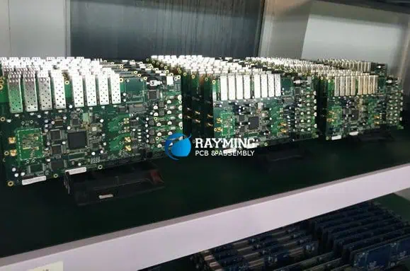
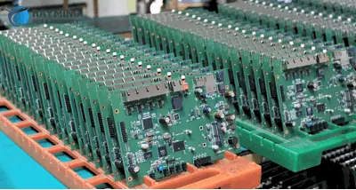
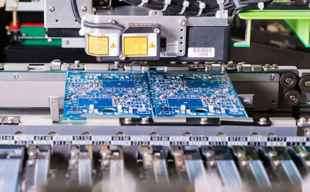
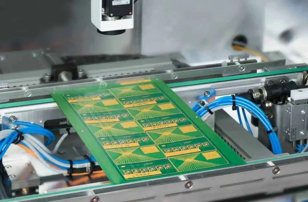
The manufacturing of PCB is a very complex task that requires using specialized equipment and engineering expertise. The advancement in technology has streamlined the major aspects of PCB manufacturing, with the introduction of lasers being one of the most recent developments.

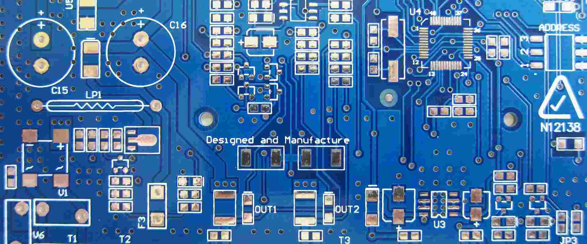
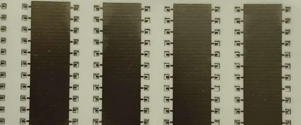
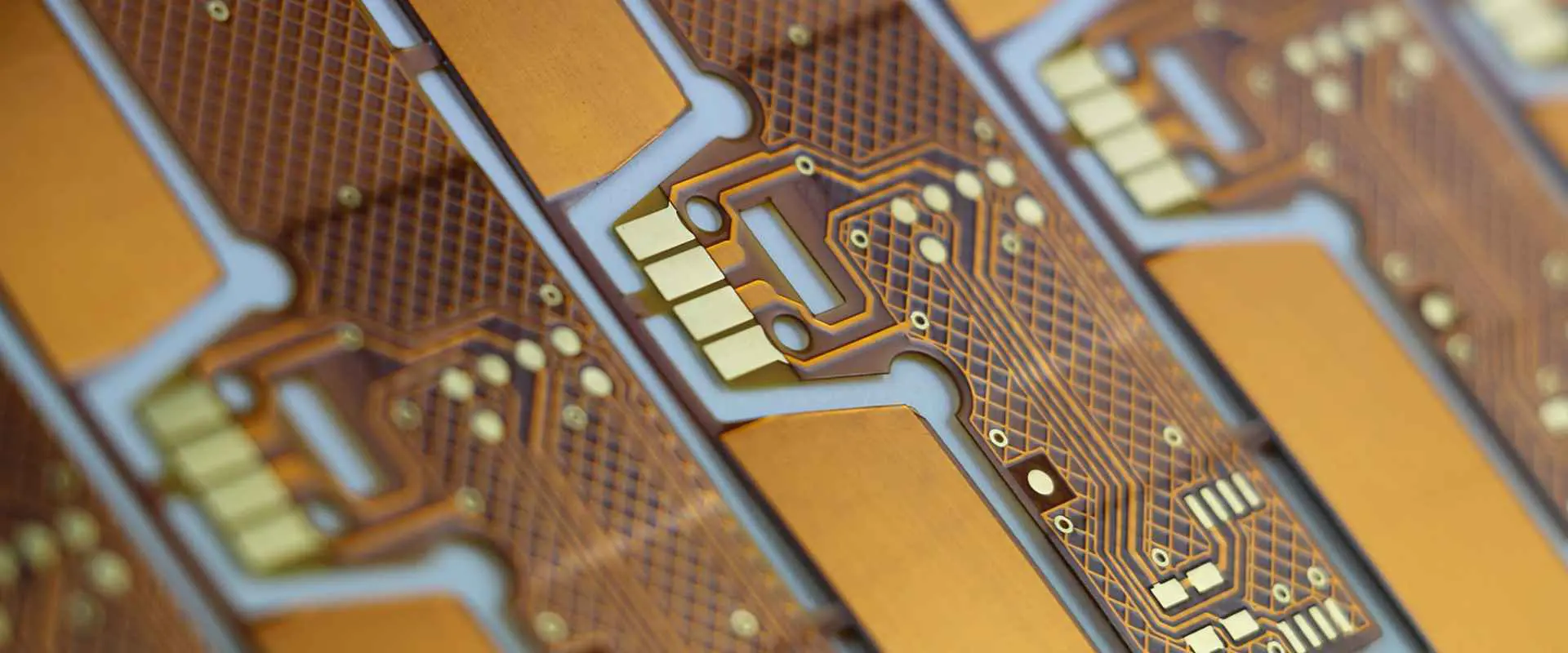
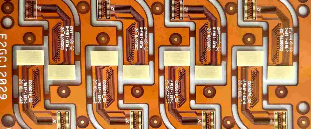
The fabrication of PCBs requires various materials. These materials are selected based on their electrical performance to ensure mechanical and electrical reliability. PCB laser etching plays a significant role in the manufacturing of PCB.

YouTube video

Lasers Marking in PCBs

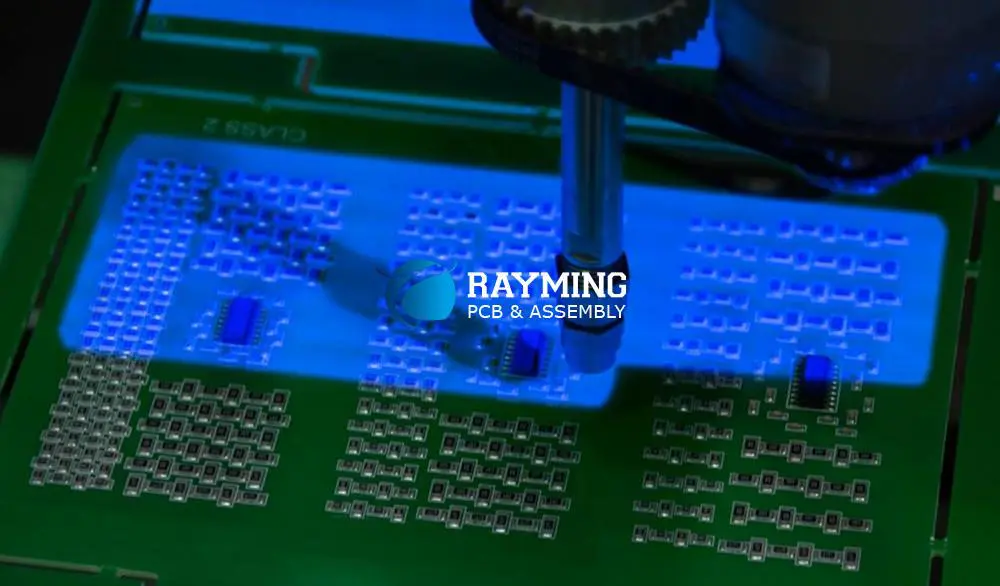
PCB  laser is used for marking circuit boards, an important step in PCB manufacturing. Since electronics manufacturing is becoming complex it is important to mark boards to determine major components and make sure that parts are placed in correct positions so that they can be well connected.

Identifying marks have become an important aspect in PCBs manufacturing. Traditionally, identifying marks are done alphanumerically, but there are restrictions due to the space available on the PCB surface. That is why lasers are used in marking PCBs since they can offer accurate marking.

Fiber laser PCB can help to include identifying codes to any PCB surface; they can use QR codes or bar codes to cram information into a smaller space.

Lasers are also very fast when it comes to marking PCBs. They can etch codes in a few seconds while preventing the material around the area of application from any damage or distortion. Laser marking also provides information in the manufacturing of integrated circuits. In this application, precision, efficiency, and precision are very important.

It is also important to know that using lasers to mark printed-board-circuits correspond with the marking of components by using the same procedure. This makes it easy to trace and replace parts while making sure that sensitive and fragile parts arenโ€™t placed under undue pressure.

Lasers Cutting in PCBs

Cutting is an important aspect of PCB production since a circuit board requires to be designed using a stencil with apertures to connect and solder components. A fiber laser can be used to cut PCB stencils in large volumes within a few seconds. The beam of a laser cut pcb can punch through the circuit board material to leave the necessary apertures thereby ensuring that it doesnโ€™t compromise the integrity of the material surrounding it.

In the case of mass production, this process has to be done repeatedly. Cnc laser pcb prevents damages from occurring and minimizes waste since they use a non-contact approach to cut materials.  Laser cut fr4 are an important aspect of PCB manufacturing.

Lasers Sintering in PCBs

Sintering is considered the perfect solution to affixing components of PCBs and this method can overcome the problems of soldering and enable more durable, stronger, and consistent bonds to form during the manufacturing of PCBs.

Laser sintering is giving opportunity for the development of cutting edge PCBs which are created without solder. High-density circuits are suitable for this technique, allowing improved stability. When sintering is done, a laser is applied to a powder that contains silver. The heat coming from the laser makes the powder reach a melting point and this is allowed to cool off to form a solid connection.

Laser Cutting and Routing Systems for the Depaneling of PCB

laser cut pcb

Laser depaneling in PCB is a great way for PCB producers to save time and money. Circuit boards contain sensitive parts that may get easily damaged and laser depaneling helps to reduce stress on these parts and their solder joints.

How to Select Laser Routing for PCB Depaneling

Laser routing is one of the popular approaches to depaneling. This procedure ensures that there is no physical contact with the board. Many producers consider laser routing to be ideal for sensitive and small PCBs used in the most recent wearable technologies.

UV (355 nm wavelength) and CO2 (10.6ยตm wavelength) are the two lasers for PCB depaneling. The relative importance of cycle time and the neatness of the cut edge are the most important factors to consider when determining the type of laser to use.

Choosing the Right Laser Source

It is important you determine the appropriate laser source for your depaneling needs. CO2 and UV lasers have their disadvantages and advantages.

UV lasers

Lasers that involve UV use โ€œcoldโ€ cutting technology. UV lasers make it easy to control the thermal charring of the edge. Therefore, a UV laser is a better option if reducing char is more vital than speed.

Pros

  • Delivers very clean cuts
  • Low HAZ
  • A narrow kerf width
  • Ability to cut copper leads accurately

Cons

  • Longer cut times
  • More expensive

When utilizing a UV laser to get clean cuts, several repetitions of laser scanning are utilized to singulate the PCBs. To control the cut speed, software controls are utilized. These cuts cut through the whole panel that cingulate the board.

CO2 Lasers

A CO2 laser is a preferable option if cycle time is very important. CO2 laser PCB can help to make full cuts and are more commonly used to create perforated cuts. Making use of the perforation technique helps to reduce char and as well as allows for easier load and unload of panels and boards from the cutting machine.

The gap left between perforations is a vital factor in the perforation technique. A bigger gap will lead to less char on the edge, but more force will be required to separate boards. We can easily adjust perforation strength based on the specifications given.

Furthermore, the amount of charring and cycle time increases as material thickness increases. If V-grooves can be used to manufacture panels at cut locations, laser cuts can be faster and cleaner.

Pros

  • Fast cut speeds
  • Allows processing of aluminum panels
  • Thicker substrates cut well
  • Lower cost for each watt

Cons

  • Larger HAZ
  • More charring on cut edges
  • More kerf width

How to Improve Cut Accuracy for PCB Depaneling

fiber laser pcb

When depaneling PCBs, the accuracy of the cut plays a significant role in reducing waste and damage. You must ensure there is consistent cut placement and this can be achieved by ensuring accurate alignment of the laser with panel components and features.

A vision system identifies certain features on the panel and adjusts the cut path to ensure the cuts align accurately to the circuits.

Why Laser Depaneling is Better Than Other Methods

  • Laser routing is a method that involves a no-contact process. This means that;
  • No mechanical stress on components
  • No sharpening or replacement of worn blades
  • Can cut through any path even curves
  • Software controls that enable simple and quick change between different cut patterns
  • No switching of mechanical parts or realigning of blades

Lasers Drilling in PCBs

Laser drilling makes holes on a printed-circuit-board to create connections between several layers. The electronic appliances we have in our homes consist of HDI boards that make use of laser drills. Laser drilling procedures guarantee accuracy even when working with small sizes.

Laser drilling utilizes laser energy for drilling a hole. This is totally different from drilling holes with a machine. Holes are drilled on PCBs for placing components and bringing interconnection between various layers. Lasers are capable of drilling between 2.5 to 3-mil vias on flat reinforced glass. It can drill about 1-mil vias when it comes to an unreinforced dielectric.

Benefits of Drilling with a Laser

There are several benefits of using lasers to drill and they are discussed below;

Precise control: Lasers help you gain control over the heat output, beam intensity, and the period of the laser beam. This provides high accuracy and helps to make various hole shapes.

Multi-tasking: Lasers can be used in several manufacturing processes like cutting, welding, sintering, etc.

Non-contact process: Lasers ensure a no-contact process and as such, there is no damage caused by drilling vibration.

High aspect ratio: The aspect ratio is an important parameter of a drilled hole. The aspect ratio is the ratio between the diameter of the hole and the drilled depth. Lasers offer a high aspect ratio since they can make holes with small diameters.

Factors to Consider During Laser Drilling

Some factors need to be considered during laser drilling, these two major factors should be considered;

The copper thickness

The lowest thickness of the target copper layer should be twice as thick as the top copper layer to be drilled. Lasers are the most effective way to make microvias in PCBs. Laser-drilled microvias are important in the manufacturing of PCBs

Non-homogeneity of the stack-up

While using lasers to drill, the non-homogeneity of the stack-up is very important. Several materials get energy at various rates. For instance, FR4 resin takes up energy at the exact rate as the glass fibers. BT epoxy resin vaporizes at a much faster rate than glass and as such, leaves glass fibers in the hole.

Conclusion

Lasers are important and specialized equipment used in the manufacturing of PCBs. These equipment are used for several purposes, they are used for drilling, cutting, marking, and sintering PCBs. Since it offers precision, this equipment is a preferable option for PCB manufacturers. Lasers also utilize the no-contact approach making it easy to use in the production of PCBs. Laser engrave PCB is used in PCB production.

Where to find a good small batch PCB vendor ?

small batch PCB

PCBs are the building blocks of electronics, and it’s essential to find a good small batch PCB vendor. Small batch PCB assembly is your ideal answer for distinct adaptability for mounting parts on a small batch of uncovered boards. If you want to dispatch an electronic product, a small batch PCB model is an outright need.

You do not need a circumstance where you are facing huge defects after manufacturing large quantities. You can also explore ways to manufacture low-volume PCBs without forfeiting on quality. It is the reason why you need to find a suitable partner that deals with low-volume assembly or small batch PCB assembly.

What you should do when choosing a PCB manufacturer

One of the most important components to consider when selecting a PCB manufacturer is the PCB’s quality. It’s not uncommon for smaller companies to slip up on quality due to tight budget constraints, but a good two-sided PCB vendor can easily catch these mistakes before mass production. Additionally, small batch PCB manufacturers should have the ability to design your project on the fly, something you can’t do when working with any larger vendor.

Are you looking for more customization options? Good PCB vendors should offer several different layer options, including FR-4, CEM-1, and Rogers 4003. The latter is preferred by top manufacturers such as RะฐัƒMing Tะตัhnะพlะพgัƒ. These boards are good for both low- and high-frequency circuits. Multi-layer boards also allow you to implement design features such as power distribution via the ground plane and signal traces on opposite sides of the board. This increases efficiency by reducing crosstalk interference and signal degradation through the unnecessary length.

If you find a manufacturer that meets your needs, you should check out their prices. Here, you submit your desired specification to the manufacturers for them to give you a quote. In most cases, you will find that proximity sometimes plays a huge role in price reduction due to shipping costs. However, you might also find a manufacturer outside the borders who offers relatively attractive prices.

You need to look beyond the price of a component for you to find a good PCB manufacturer. Some other factors you should consider include the quality and types of the PCB they produce. For example, you would not want to be in a position where you are getting a video game board from a vendor specializing in washing machines.

The small batch PCB manufacturer should also have a wide range of manufacturing processes. Many vendors have just a few options such as SMD, CSP, and AO that are both slow and expensive. These considerations should include the plating, via clearance, and the way traces are routed on the board. If you intend to print your PCB with a 3D printer or silk screen PCB, look for vendors who can provide custom stencils for some of these processes.

On top of pricing, you should also consider the PCB manufacturer’s turnaround time. Typically, a two-layer board can be produced in one day or less. However, many small batch PCB vendors offer next-day delivery for orders placed before noon. In some cases, 24-hour turnaround is available for the same day or next morning delivery. This ensures that your project won’t get delayed while waiting on parts, and you can start integrating the PCB into your project as soon as it arrives in the mail.

Taking everything into account, a few elements influence the expense of small batch PCB assembly. Significantly, you pick an organization that meets your innovation needs and meets your financial plan. If you are searching for an approach to decrease costs, attempt to plan a antenna PCB with a couple of special parts from a nearby producer with a great deal of time to finish the undertaking.

How to profit from outsourcing small batch PCB

FULL PCB MANUFACTURING Quote

The following tip will help you get the most when you outsource small batch assembly and give you a rewarding experience.

  • Review your custom materials with your manufacturing partner

If your manufacturing partner uses customized parts, sourcing difficulties may emerge. It is usual for the manufacturer to encounter growing minimum orders, unexpected price increase, material obsolescence, and other challenges.

To forestall materials issues from happening at a crucial time, ask your manufacturing partner to lead a quarterly or semiannual survey with you about your tweaked material necessities.

  • Divide and rule

It is critical to see the value in why a believed partner may decide to pass on your business. For example, re-appropriated PCBA producers can deal with a particular scope of manufacturing batch volumes. However, if they produce more than their capacity, it might mess conveyance all through their client base, including you.

If you realize you will have bunches that shift extraordinarily in necessities, think about working with two small batch PCB manufacturers. One should have the capacity for small batch PCB assembly production and another for large batch PCBA production. It permits you to benefit the two suppliers and guarantees you will generally have a certified partner to go to.

  • Clearly state your technical requirements

Reevaluated PCBA fabricating organizations work with various customers, each with their one-of-a-kind specialized details and needs. It is the reason why you give your assembling company your detailed prerequisites front and center. It is undeniable when you bring another item into the market or have certain corrective adequacy principles or different necessities that fluctuate from the business standard (IPC) rules.

  • Voice your concerns and problems

Even though it tends to be costly and risky to change contract producers, the basic industry practice is to move the business to another provider instead of dealing with an exhibition concern directly. Thus, the best solution is to talk about it. Regularly it is not simply the issue but rather how your provider reacts to it that forms certainty.

Partners that cannot handle it will keep away from struggle, which may lead to serious damages in the long run. Commitment, trust, genuineness, and honest talks help create great business associations. These factors foster a suitable environment for the growth of a personal relationship over time.

If there is something significant you have keeping to yourself, it is high time you told your batch PCB assembly manufacturer. Despite how long you have been functioning with them, make certain to voice your interests, so your issues stand out enough to be noticed and get a solution.

Advantages of using small batch PCB assembly

small batch pcb assembly

Every electronic device must have and depends on a printed, electronic circuit board for proper functioning. As gadgets keep advancing across ventures, more organizations understand the expanded requirement for quick equipment improvement.

To stay serious and essential, organizations are continually improving and advancing new products. It implies going through item advancement and deliveries a lot quicker than expected. That is why progressively more organizations are picking the small batch PCB instead of full large-scale manufacturing. The advantages include:

  1. Quality products

By embracing the low volume PCB, advancement technicians can work straightforwardly on client reviews from prior products to create a better version. Similarly, as programming continually needs fixing and refreshing, the equipment can likewise profit from improvements.

More organizations, particularly new businesses and crowdfunding projects, firmly depend on reactivity with its allies, gain from this advancement style. It eventually brings about a better item customized than the objective market.

  • Cost-effective

Ventures used to get ready for large-scale manufacturing runs might be reluctant to change to small batch PCB. Yet, it looks bad to create an excess for commonality. The quantity of ‘valuable’ PCB dominates the expense per board may diminish fundamentally.

It does not bode well to deliver a huge number of boards in one go if you expect to sell a couple hundred every month. It is self-evident if the plan is as yet a work in progress or long haul stockpiling might be an exorbitant cost.

With serious rivalry, fickle business sectors, and increasing demand for innovation (cell phones), it has less sense or reason for large-scale manufacturing.

  • Quick Turnaround

It is simply sound judgment that small batch assembly is easy and takes less time. It is valid for both arrangement and the actual assembly process. The smaller the batches, the less the rate of defects. The low number of defective boards does not legitimize careful trials and plan alterations to resolve the source of imperfections. A lot of testing, however, is excessive on a large scale manufacturing.

Here is the place where the skill and adaptability of a lithe producer come in. The repair technicians and quality architects manage a sufficient assortment that such issues are recognizable and can sort them out productively and without any problem. It is ideal when an opportunity to advertise is of outright principal significance, and improved varieties are underway.

Some turnkey PCBA administrations offer uncommonly speedy turnaround times. By including board manufacture and parts procurement in their contributions, they can smooth out the whole assembly and improve proficiency.

Factors that influence the cost of small batch PCB assembly

There is a lot that goes into PCB assembly that will determine the costs. They include the quantity needed, packaging of parts, turnaround time, technology, and labor cost. The utilization of a PCB-producing cost mini-computer can help you identify the expense of the activity. In any case, most PCBA unit costs range somewhere in the range of $10 and $50, relying upon the quantity of units manufactured.

Generally speaking, the expense of small batch PCB assembly can shift broadly by the manufacturers. The variables that influence the expense of PCB assembling include:

Parts Packaging

A few sections include more work to bundle and appropriately collect. For example, electric gear like BGAs requires additional time and exertion to bundle since they should be associated with an electrical source. Since BGAs have electrical pins, gathering expenses can shoot up drastically since they should go through an X-beam assessment to check for short-circuiting.

Innovation

A vital part of small batch PCB assembly valuing is the sort of innovation utilized. On the one hand, SMT can give cost reserve funds to producers since arrangement costs are lower. Be that as it may, SMT can bring about the requirement for through-opening boring to fit extra surface mount devices (SMDs), driving up the costs.

Quantity

With regards to assembling, large quantities lower the assembling cost because of economies of scale. As such, companies manufacture products at a bigger scope, the unit cost of each PCB drops altogether. This financial marvel happens because large numbers of components drive up assembling costs. Similar to startup expenses and programming, they influence the underlying units delivered.

Expanding the number of PCBs manufactured can set aside firms’ cash over the long haul.  They do him by forestalling one-time costs that do not need reproduction. In this way, you ought to consistently search out makers that can oblige the huge request.

Turnaround Time

Turnaround time alludes to the range of time needed to finish the assembling cycle and fulfill the purchaser’s solicitation. When in doubt, quicker turnaround assumptions come at a greater expense.

Purchasers that request short turnaround times pay more for PCB assembly by approximately 33%. In general, short turnaround times will expand assembly evaluation since it regularly expects firms to stop existing requests to focus on yours. In like manner, assisted transportation reduces the turnaround time and costs more than customary delivery.

Labor Costs

The geological area from where an organization produces the PCB greatly influences the labor cost. Since PCB fabricating includes automated machines and skilled human processes, the work expenses can be huge. So, firms have an impetus to produce PCBs in districts where work is less expensive.

For example, a PCBA in South Asia is, for the most part, a few times more affordable than one in Western Europe or North America. The normal small batch assembly expense in North America is generally $1,500 in US dollars for a three-day turnaround time. Conversely, a similar amount of PCB in China is $526.

Assembling abroad can increase costs because of communication delays, handling, and shipping. In this manner, a small batch assembly can incorporate unanticipated costs that one should account for before importing PCBs.

Summary

A good small batch PCB vendor can help you get your design into production without undermining the quality and reliability of your circuit. Don’t forget to keep these things in mind when selecting a small PCB vendor for your next project:

1) Make sure that the vendor has a positive reputation

2) Check if they have a solid online presence, both locally and on the web.

3) Make sure that they offer quick turnaround times and clear communication with customers.

4) Be sure to ask for details about design and assembly options, including layers, design rules, and parts availability.

5) Check out what the turnaround time will be for your project. Again, they should have a variety of options for you to choose from.

6) Do a little research on the vendor’s quality control processes and use this information when making your decision.

This guide is here to help you make the right choice when selecting a PCB vendor for your project. If you’re ready to get started with your design, find out how easy it can be with RะฐัƒMing Tะตัhnะพlะพgัƒ! Check our blog for the latest updates on new features and other industry news.

What is PCB CTI?

PCB CTI

Concerns about electrical safety are not isolated to electrical boxes or other equipment of high voltage, distribution lines, and transmission, caps, and transformers. PCBA, which includes virtually all systems, appliances, and devices that we make use of, can be dangerous if there is an occurrence of contingency where there is an exposure of users or personnel to extreme current level. This is more likely to happen for industrial boards of which high current printed circuit board tips and guidelines for designing should be adhered to.

YouTube video

What Does The Comparative Tracking Index Mean?

The comparative tracking index is similar to the high voltage arc tracking rate (HVTR), it evaluates or measures the capability of a Printed circuit board surface to withstand tracking. In this case, tracking refers to faulty insulation materials that exist between conductive surface elements like traces and pads.

A printed circuit board is utilized to offer mechanical help and to interface electrical elements electronically by utilizing conductive pathways, the signal follows or tracks engraved from copper sheets covered onto a non-favorable substrate. Comparative tracking index is the ability to which Printed circuit board materials that have the insulating capability of resisting unneeded current to have flowing access on the board between traces.

It is the measurement of the capability that the Printed circuit board underlying support has to confront any failure or crack-down between double tracks on the outside layer of the printed circuit board materials. It is made use of in assessing the level of resistance of the printed circuit board base material and assists in calculating the high-voltage segregated or in solitude values between the tracks.

PCB CTI Value

PCB cti value

The comparative tracking index value depicts the resistance of the printed circuit board materials against ecological influences like moisture and dirt. This is well explained in terms of when the value is higher, then the higher the material is, the more resistant. FR4 CTI has a default comparative tracking index of 175 and which may increase to about 600 unique materials.

The worth of comparative tracking list is learned with the utilization of standard test techniques Tracking resistance is the refusal and opposition against the current flow put forward by the Printed circuit board. The rising in the digit of elements placed on the printed circuit board increases its general packing density; this contributes to little trace spacing. Hence, the CTI value in the printed circuit board base material is very essential.

These values contribute to the reduction in the general printed circuit board resistance to tracking. These values provide an evaluation for loss of electricity most especially as a result of faulty or breakdown insulation or short-circuit as trace spacing gets reduced as a result of the elevated number of elements. On the basis of the standard set by the IEC, the smaller comparative tracing index grade substratum provides great resistance to electrical breakdown.

A comparative tracking index is a number that is critical while picking a printed circuit board material. The range of a normal FR-4 CTI is from 175 to 225V.

The increment in the packing density of elements on the printed circuit boards increases smaller conductor track spacing. Thus, the PCB CTI value in the base material data sheets becomes increasingly more essential. This is the scale for resistance tracking.

Comparative Tracking Record

Comparative tracking record is the technique for estimating a material as an electrical encasing and is given as the voltage at which while going through a trial of normalization, the outside of materials separates. Comparative tracking index numbers for products are published by the Printed circuit board laminate manufacturers.

Here comparative tracking index is an item of good quality which is applicable to Copper Clad laminate which is mostly used in domestic electronics or electrical apparatus with a voltage at a high rate (110V, 220V). It is a dummy situation that the Printed circuit board in its work environment suffers from pollution, which leads to short-circuiting or leakage at the track gap of the Printed circuit board surface, of which charring and heat-releasing is the companion.

The method of experimentation is that continuous 50 drops of 0.1% ammonium chloride solution are released along with the dual points on the Printed circuit board surface, half a minute per drop, switching on high voltage AC current to do the testing.

The first instance is trying 300V to generate a 1A current. On the outside layer, there is a solution with ammonium chloride, so after switching on the current, resistance will be produced which also generates heat, after which the solution evaporates slowly. The second drop is on and goes till 50 drops to observe if there is leakage with the Printed circuit board or not. Once there is a creepage of 0.1A and goes above 0.5 seconds, itโ€™s said to have failed.

There are high PCB CTI (increased CTI 600 pcb material backed by aluminum, CTI 300, and CTI 600v PCB) which works in such a difficult environment of humidity, filth, and high voltage.

It must be stated that the most important aim of all standards for electrical safety is preventing any danger caused by shock. On that basis, the creepage and clearance allowance among its conductors that are prone to the voltage that is hazardous can be the lowest that guarantees the circuit will be functioning and not deteriorating.

IEC-60950-1 highlighted five accelerating levels of compulsory insulation that are related to the physical location of a circuit that is relative to contact by humans, operating environment, and the voltage. Naturally, the best approach in avoiding the degrading circuit or danger of shock is to space traces distance away apart as much as possible, but most times, that distance doesnโ€™t/ will not meet the requirements of creepage.

If looking towards the angle of a material with a good Comparative tracking index seems impossible, routing a slot between two traces can add to the creepage distance. The loss of electricity due to faulty insulation from one trace to the other on the laminate surface would need to move around the air gap. However, a vertical hindrance of insulating components could be stationed in the space, which would add to both the clearance distance and that of creepage.

Importance of Comparative Tracking Index

CTI 600 pcb material

HVTR testing and other high-standard voltage arcing tests are carried out on dry, solid insulation materials. Comparative tracking index testing is carried out with the application of liquid to the board surface. It is aimed at evaluating the opposition of the boardโ€™s insulation to track. In the presence of contamination, which is most likely for industrial boards, especially when entrenched in manufacturing equipment, as discovered in advanced industrial processing environments.

The Comparative tracking index is significant as it gives a quantitative metric by which materials that differ can be compared and a selection possible based on its chances to cope with its intended environment. Most especially, the Comparative tracking index can be adopted to ascertain clearance distance and creepage for your boardโ€™s design.

Comparative Tracking Index Testing Options

  1. UL testing facility: The best option is by testing by anUl facility if testing is needed. The Comparative tracking index test can be carried out with the related surface tracking estimation.
  2. Facility for other testing facilities: There are several companies that can carry out testing of materials for you. The benefit here is that you are not mandated to acquire or have the equipment that is necessary or the environment that meets the standardsโ€™ requirements.
  3. In-Door: if your anticipation is on the need to carry out this type of testing regularly, the expenses might worth acquiring equipment and expertise to get it done whenever it is required.

Additionally, you may make use of the result of past studies that are available, and that is compatible with your design. If accurately utilized, Comparative tracking index testing can assist you in picking the best materials, PCB layout, and coating that are protective for your industrial board.

Understanding CTI in line with PCB routing

In case when two PCB traces similarly and often happening at the same time, the dielectric materials should not at any time break down, and the dual traces should have the ability to carry current without any glitch. There are fewer chances of dielectric breaking down and direct shots. The dielectrics make sure that there is a presence of resistance at the dual traces.

One of the basic reasons why the dual traces might have a loss of electricity is as a result of the formation of contamination between traces, the voltage applied, temperature, and ecological conditions.  Comparative tracking index is the proportion of the susceptibility of the printed circuit boardโ€™s insulating materials to the electrical breakdown. Mathematically, the Comparative tracking index represents the voltage, which results in failure by breakdown after 50 drops of 0.1% ammonium chloride solution have failed on the material.

Creepage Distance and Comparative Tracking Index Value

Creepage distance is the shortest available path between the measured dual Printed circuit boards along the insulation surface. Depending on the Comparative tracking index value of the Printed circuit board, the creepage wild will experience a difference in value.

 If the Comparative tracking index records a higher value, then the minimal creepage value is needed. Lastly, a high Comparative tracking index value indicates the close tie between the Printed circuit boards.

Conclusion

In the fabrication of printed circuit boards, CTI is the measurement of the capability of the laminate external layer to be able to hold the outside layer, upon the release of an electrolyte between them.

How to Waterproof Your PCB ?

Waterproof pcb

When we design a PCB board, it is inevitable that we have to face the problem of a wet environment, such as the rainy days or steam in the factory. Under this kind of situation, the circuit board will easily get damaged. In the past, we had to pay great attention to the design of PCBs and use waterproof material and special processing technology to make it waterproof. However, the complex process and high cost have made the PCB sales price higher than others. Nowadays, there are many kinds of techniques with high reliability to make a PCB board waterproof. We can use them to replace traditional methods.

YouTube video

How to Waterproof Your Electronics or PCBs:

It is always suggested that the PCB boards should be protected and stored in a dry place. It is a great idea to put the PCB boards in the sealed bag. Thus, PCB boards will not be affected by water and will not get wet even if it rains hard outside.

There are many ways to waterproof PCB. We can choose one according to our needs.

1.Apply waterproof material on PCB board

This method is used for very special purposes, such as making PCBs for control systems of ships or submarines, etc. In this way, you can add some special material on the surface of the PCB board to make it waterproof, such as Parylene C or Parylene N, etc. In fact, Parylene C and N are the same material. They are both high-density polymers, which can be made into thin layers. Generally, they are in liquid form when we apply them on the PCB boards. They will be solidified after a certain time, and become waterproof. The thickness of Parylene C is around 2 mils (0.05mm), which is much smaller than that of traditional varnish (such as epoxy resin). If you need to make your PCB board waterproof, you can choose Parylene C or Parylene N as your material.

2.Use Waterproofing Material to Seal up the Connectors

If you want to make a waterproof PCB, but not for special purpose, you can choose to use waterproof materials to seal up the connectors. The connectors are mainly used for connecting the wires and other components, such as wires, terminals and sensors. The connectors will be in contact with water directly when they are in use. If they are not sealed up carefully, the water will penetrate into your PCB board. When it happens, your electronics or PCBs will be damaged easily.

3.Apply special waterproof paint to the PCB board

If you need to make a waterproof PCB but you do not want to use special materials, you can use some paints. They are usually used as a protective layer. It is easy for you to apply them on the surface of the PCB board. The main purpose of these paints is to protect the surface of the PCB board and make it smooth. However, they can be applied on the PCB board with high quality and low price. If you choose this method, it is suggested that you should select the best waterproof paint for your PCB board.

There are many kinds of waterproof paints on the market, but they are not all reliable and efficient enough.

Which application process is better? Dispensing, manual spray, or dipping?

PCB circuit board waterproof coating

1.Dispensing

This application process is the most commonly used to paint PCB boards. In this process, paints are stored in a hopper and then pumped into a gun. The paint will be sprayed onto the PCB board with the help of a spray gun.

2.Manual Spray

This process is similar to dispensing, but manual spray can be used when you do not have a special painting machine or there are many different PCB boards for painting, which cannot be painted by dispensing. It is better to use manual spray rather than dispense method if you can because manual spray allows you to paint with high precision and makes the surface of PCB board smooth.

3.Dipping Process

In this process, the PCB board will be dipped into the paint tank to be coated. It is a common process in the industry. However, it is really not recommended for you to use the dipping process when you are making PCB boards and electronics, because PCB boards should have some thickness. If you dip your PCB boards into the clear coat, most of the clear coat will stick on the surface of the PCB board and some will remain in the paint tank. This will result in uneven PCB coating of clear coat on the PCB board.

Every PCB has an Achilles heel: water. Is there a solution beyond conformal waterproof coatings?

The conformal waterproof coating is known as one of the most useful and popular materials used to protect PCB boards. It is a thin, elastic, protective material that can be sprayed on the PCB board to make it waterproof. It can be used to protect PCBs in many different environments. However, in spite of its wide application, conformal waterproof coatings have some problems. They are not effective enough to protect PCB boards under certain circumstances. Generally, there are two main reasons for this situation:

1.The conformal waterproof coating cannot effectively prevent water from penetrating into the PCB board because of its low adhesion strength.

2.Even if the conformal waterproof coating can prevent water from penetrating into the PCB board, it will be damaged in a wet environment or when the environment is too corrosive.

In the past, PCB manufacturers just used conformal waterproof coatings to protect their PCB boards. They did not have any other solution, and they did not find another way to solve this problem. That is why they always had to pay attention to the design of the PCB board and use special PCB materials to make it waterproof.

I Use Waterproof Enclosures. Why Do I Need Conformal Coating?

Conformal coating is not the same as an enclosure. However, you will use enclosures if you need to make your electronics waterproof. The enclosure is used to protect your electronics from water and air. It is like a tent that can protect your electronics or PCBs from water, air, corrosive gases and other harmful factors.

Generally, conformal waterproof coatings are sprayed on the surface of PCB board to make it waterproof.

So which one do I need?

1.If you want to make your electronics or waterproofing circuit boards, you will need both conformal waterproof coatings and enclosures for sure. If the environment is too corrosive or wet, it is recommended that you should use both of them together. In some cases, you will need to make your electronics or PCB boards waterproof only. In this case, you can use conformal coatings without enclosures. You can use conformal coatings for PCB protection against moisture in wet environments and corrosive environments. It is highly recommended that you should use conformal coatings to protect your electronics or PCB boards in wet and corrosion environments.

2.If you have a special purpose for making a waterproof PCB, you do not need to use conformal waterproof coatings at all. For example, when you are making PCBs for the control system of a ship or submarine, etc., there is no need for these kinds of materials because it is not allowed that water penetrate into the control system which can cause the ship and submarine to sink.

There are many ways to waterproof circuit boards or your electronics. You can choose one according to your needs. If you need to make your electronics or PCBs waterproof in a wet environment, it is recommended that you use a conformal coating first, and then enclosures. In this way, your electronics or PCBs will be well protected, not only from water but also from corrosion and other harmful factors.

How do you test or check if the coating is on the surface?

There are two common ways to check if the coating is on the surface or not.

1.The first method is to test the surface with some other types of coatings such as epoxy resin or silicone. If you use the above types of coatings, they will not stick onto the surface of your PCB boards if the surface is coated by conformal coating application.

2.The second method is to use alcohol spray and then see if there are water droplets on your PCB board. If there are water droplets, it means that your PCB boards are coated by liquid conformal coating.

Does the applied thickness impact conductivity?

Normally, if you use too much conformal coating application, it will make your PCB board more conductive. However, it depends on the thickness and type of materials you use for making your liquid conformal coating. If you use high-quality materials with good electrical conductivity, it will not affect the conductivity of your PCB board.

Are there disadvantages for a surface that has been over-applied or applied to be too thick?

When you apply too much conformal coating materials, your PCB board will not be able to have effective heat dissipation and electricity efficiently. It will result in a huge heat dissipation and electricity which is very harmful for your electronics or PCBs.

Do you need to apply conformal coating on solder terminals?

You can spray the terminals with conformal waterproofing coating, but it is not recommended because it can cause some problems such as short circuit, poor conductivity, etc. The solder joint is mostly used in electronics and PCBs to connect components together. It is actually not an electronic component itself. The solder joints are never covered by any conformal coatings. If you apply conformal coatings to the solder joints, the conductivity will be decreased and it will cause poor performance of your electronics or PCBs.

You also need to pay attention to the weight of the PCB board. If you apply too much conformal waterproof coatings on the surface of PCBs, it will be heavy and unbalanced. The heavy and unbalanced PCB board may cause failure in the process of assembling.

The Difference between PTH and NPTH in PCB

pcb pth

Through Hole PCBs

Printed Circuit Boards electrically connect electronic components through conductive pathways, tracks or signal traces that are etched onto a copper-plated sheet. The PCB board itself is made of a non-conductive substrate and has several holes drilled through it. These holes are drilled with coated, solid, tungsten carbide drill bits and are prominent in diameter. The holes are made conductive by electroplating with copper.

YouTube video

By using PCBs โ€œthrough-holeโ€ or โ€œthru-holesโ€ technology, electronic components are mounted onto the substrate using the componentsโ€™ legs (or leads). The leads are placed into the holes and soldered onto pads on the opposite side through manual assembly (placing by hand) or using automated insertion mount machines.

Printed circuit boards may have different sized holes, which are differentiated as PTH (Plating-Through-Hole), which has been described above, and NPTH (Non-Plating-Through-Hole), which have no coating as they are not used for conducting pathways.

PTH Vs. NPTH

PCB pth npth

PCB pads are the exposed metals on the substrate where the component lead is soldered. Multiple pads are used synchronously to create a land pattern (component footprint) on the PCB. Pads can be through-hole ones or surface mount pads. A hole is considered PTH if its pad has copper along with the solder stop mask. This should be larger than the hole/slot with a minimum of 6 mils in width and be overlaid.

Holes in which the pad’s copper size is smaller than the hole or if there is no copper at all are NPTH. Also, even if the pad’s copper is overlaid or larger than the hole, there will be a six mil space of clearance between the copper and the hole.

The manufacturing process of NPTH is simpler, hence quicker. They are most used (but not always) as Tooling/Mounting holes to fix the PCB to its operational location.

Land Patterns and Component Footprints

The most important part of printed circuit boards is their circuits that interconnect electronic components. Most of the time, components are soldered to PCBs, but soldering can only be done under conducive conditions in order to be effective. The leads of a component must have a consistent electrical and mechanical connection to the etched copper traces.

Also, each component must have a footprint or land pattern. This footprint is how the pads are arranged in through-hole technology or surface-mount technology and are used to attach and electrically connect components to the PCB physically. The component’s land pattern is the etched copper features that matches the leads of the component. These land patterns are normally made slightly larger than component leads to allow soldering space.

Since most PCBs are double sided, or multi-layered, it requires plating of the Through Holes are plated, so that components can connect with each other and with required layers in the board.

How can you tell the difference between PTH and NPTH?

The easiest way to distinguish between Plating-Through-Hole and Non-Plating-Through-Hole PCBs is by visually checking for traces of plating on the borehole wall in the PCB. Non-Plating-Through-Hole PCBs will not have any traces of copper in the borehole wall.

Plated-Through-Holes PCBs are more expensive than non-plated-through-hole PCB. Also, PTH printed circuit boards are often smaller than NPTH printed circuit boards.

The Use of Plated-Through-Holes in PCBs

A plated-through-hole PCB works best for the ceramic diamond copper plating, copper plating, and resin copper plating, amongst others. These PTH holes have two purposes:

  • Component holes for welding DIP components.

In such cases, the hole diameter must be larger than the pin of the component so that the component can be inserted in the PTH.

  • โ€œViasโ€

Vias can be between outer and inner layers, or inner layers only, or from surface-to-surface. They connect and conduct wiring between different layers in PCB. The size of these PTHโ€”Plating-Through-Holes will be smaller than component holes. PCB vias should ideally provide conductive paths, passing electrical signals from one layer to another to integrate each PCB layer they pass.

The Use of Non-Plated-Through-Holes in PCBs

NPTHs are simpler PCBs. Therefore the manufacturing process for these is faster. They are frequently used as Tooling/Mounting holes, to fix the PCB to its operational location. They are also used to mount components in some single-sided PCBs.

PTH Components Handling Processes

PTH or Plated-Through-Hole PCBs are ones in which the leads (or legs) of electronics components are inserted into designated โ€˜holes’ in the printed circuit board. These are soldered into place using a number of soldering techniques such as using a hand solder, selective soldering, wave solder, or intrusive reflow process. This entire process is called conventional assembly. Soldering forms very strong joints as the component are soldered completely through the PCB and not just onto the surface of the PCB like Surface Mount Technology (SMT) components.

The components inserted in a PTH PCB are done through these automated processes:

  • radial insertion (electrolytic capacitors),
  • axial insertion (resistors and diodes),
  • odd form insertion (connectors, transformers, etc.) or
  • manually (by hand.)

Drilling Rules for PTH and NPTH PCBs

Some general rules should be applied to the NPTHs and PTHs that you are designing and manufacturing. These rules can significantly impact the turnaround time for your board.

Non-Plated-Through-Hole (NPTH) Drilling Hole Rules

  • Minimum edge to edge clearance (from any other surface element) = 0.005โ€ณ
  • Minimum finished hole size = 0.006โ€ณ

Plated-Through-Hole (PTH) Drilling Hole Rules

  • Minimum edge to edge clearance (from any other surface element) = 0.009โ€ณ
  • Minimum finished hole size = 0.006โ€ณ
  • Minimum annular ring size = 0.004โ€

When considering simple PCB Design For Manufacturing (DFM) rules and guidelines for drill holes, consider drill hole sizes, spacing and aspect ratios, and via types. If your DFM purpose is space-saving, use via-in-pads. Alternatively if DFM requires faster turnaround time, explore alternatives via options. You are employing via-in-pad increases the PCB manufacturing process by two days.

Annular ring dimensions are important for through-hole designs. The annular ring is the copper area extending past drilled holes on PCBs. If the PCB annular ring is too small, the copper around the hole may easily detach when heated during repair or when subjected to mechanical stress. The recommended annular ring value for any NPTH hole is 0.30mm (12mil)

The Reason NPTH Use Declined

Non-Plating-Through-Hole PCBs have simple features that are either drilled or milled through your circuit board. Since components do not have copper-plating of conductive copper, the hole has no electrical properties. NPTHs were popular when PCBs had copper traces printed on only one side, but waned as multilayer PCBs became common. Now they are mostly used as mounting holes to allow screws or other fasteners to pass through PCBs.

Why Surface Mount Technologyโ€”SMT is now Popular

Now SMT Surface Mount Technologies have almost completely replaced through-holes because they reduce the production cost, increases automation, and improve quality.

The mounted electrical component of an SMT is called a surface-mount device (SMD). They are popular as SMT capacitors and SMT resistors. Since SMDs can be made very small, SMT can hold many more components on a given area of the substrate.

Advantages of PTH Production

The mechanical bonds connecting components to the circuit board are much stronger in PTH assembly than those produced by surface-mount methods. Faulty connections can be repaired individually by hand rather than by replacing an entire circuit board. However, PTH PCBs are more expensive.

PTH assembly is used for bulky components, such as large package semiconductors that need high mounting strength to withstand high stresses or in electrolytic capacitors, such as in electronic modules, power supplies, and the assembly of LED applications.

Since investors demand less equipment, lower costs, fewer manufacturing processes, and higher profit yields, process and design engineers have evolved a mixed technology that uses through-hole and surface mount methods together in a two-phase process.

Cost-Effective Ways to Lower Manufacturing Costs for Plated-Through-Hole PCBs

Annular rings, hole density, and hole design/size all affect your PCB cost. Here are tips to decrease costs.

Larger Annular Rings:

Minimum annular ring size is defined as the border of the holeโ€™s and the padโ€™s minimum distance for hole pads and vias. PCB costs increase if the minimum annular ring is less than standard requirements.

Lower Hole Density Per Square Meter:

The machines for mechanical and laser drilling each have their own efficiency. Higher hole density per square meter, take longer to complete the drilling process during PCB mass production runs; it is recommended to decrease hole density per square meter if your PCB design supports it, as it lowers costs.

Larger Holes:

Drilling small holes requires high-precision machines, which cost more. PCB fabricators upcharge for holes between 0.15mm and 0.3mm in diameter, so it is better to use larger diameter holes and annular rings.

Hole Shape:

Holes can be either round or oblong. Round through-hole pads or vias annular rings are uniform around the hole, while dimensions of oblong-shaped through-hole are non-uniform. Though the shape doesnโ€™t matter, for both, larger annular rings cost less and increase PCB quality and efficiency.

If you need more information on through-hole technology and PTH assembly, or to determine PTH and NPTH manufacturing costs, contact us to learn more.  We are happy to answer your queries.

The Important Dynamics of PCB Creation

pcb creation

The world is awash with the digital revolution, something that incorporates computer codes and electronics. Because of this, electronic engineering and design become pivotal for any tech advances. But can you talk of electronic design and engineering without factoring in a printed circuit board (PCB)? Therefore, it becomes crucial to understand what it all entails, the methods of creating one, and where you can get such PCBs. So why not dig in and look at what it all entails besides how you can create one.

YouTube video

Definition of PCB

PCB, an abbreviation of the printed circuit board, implies a board that electrically and mechanically connects electronic components through conductive pads, tracks, and other attributes etched from singular or more layered sheets of copper laminations between or on sheets of substrate that proves non-conductive.

PCBs exist in different forms, and this often depends on the mechanisms used to develop them. An excellent example includes the EAGLE PCB that uses the EAGLE technology in creating the PCB. Additionally, such printed circuit boards get manufactured by diverse companies across the world. As a result, the quality and price of the PCB often differ with the company manufacturing, assembling, or testing the PCB. Therefore, if you want an excellent PCB, it would prove better not to look further from the RayMing PCB & Assembly Company.

Creation of Printed Circuit Boards

PCB creation software

PCBs prove such a common aspect for electronic design and engineering that most people often forget to understand what it all implies. But since we have gotten that out of the way, it becomes crucial to comprehend how to create one. Before, circuit boards entailed a connection of point-to-point wiring, a laborious process that often led to short-circuiting incidences whenever the insulations wore off. However, with time, the tech moved to integrated circuits and silicon, which saw a decrease in cost and the size of the circuit boards.

Understanding how to create a printed circuit board becomes instrumental in knowing what components make up a PCB. So why not delve into this first before proceeding to the PCB creation?

Components of a PCB

A printed circuit board contains four main components: the substrate (FR4), copper, soldermask, and silkscreen.

  • Substrate (FR4). The substrate or FR4, the base material, comprises fiberglass, and it provides the PCB its solid core through its thickness and rigidity. However, it becomes vital to note that other PCB substrates can include high-temperature and flexible plastic like the Kapton or equivalent.

The thickness of the PCB substrate differs, and often this can range from the 1.6mm of the SparkFun products to the 0.8mm thickness of the LilyPad boards.

  • Copper. The copper layer comes as a thin foil that gets laminated into the board with an adhesive and heat. The copper layer can be applied to both sides for the double-sided PCB, while a single layer applies to the one-sided and less expensive PCB. However, for the double-sided board, the copper layer can range from one to an excess of sixteen layers. The thickness of copper gets specified as ounces for every square foot.
  • Solderrmask. It comprises the immediate layer resting on the copper and provides the PCB its green color. The soldermask aims to insulate copper traces, especially from accidental brushes or contact with metallic substances, conducive bits, or solder. It also assists the user to correctly soldier the right spots and limit solder jumpers. Please remember that the soldermask can also come in other colors, as green often proves the prevailing color.
  • Silkscreen. It encompasses the white layer incorporated into the soldermask. It adds the numbers, symbols, and letters to the printed circuit board to permit easier comprehension of the board besides assembly.       

Now that you understand the different components that make up a PCB, we can now delve into the PCB creation process.

Creating Your Printed Circuit Board

Are you an electronics designer with a unique design of which you want to create a PCB circuit prototype but lack the technical wherewithal to do it? If so, then consider the following steps to create a functional PCB.

  • Assemble all the materials and tools you will need for the PCB. Here, you have to get a flat iron, mini-drill, latex glove, laser printer, and some form of eye protection. Additionally, get the required materials such as glossy/ magazine paper, etching solution, marker (fine-tipped), PCB board, sanding paper, a cloth piece, and a ruler.
  • Design your PCB board. You can accomplish this in diverse ways, though it becomes crucial to develop a PCB layout using a good PCB design program such as the EAGLE editor. However, if you possess a layout (PCB) already, you can skip this process. Additionally, you can write whatever design you fancy straight on the PCB board, especially if you do not plan to print.
  • Print your printed circuit board layout. You have to ensure that you use the laser printing technology (laser printer), though a photocopy can also work. However, you must use the magazine or glossy paper for printing purposes.   
  • Iron the PCB layout after printing. After finishing the printing process, you have to iron your PCB layout using the ordinary laundry iron. It will transfer the ink onto the printed circuit board. However, take care and ensure that your iron’s set temperature reflects the thickness of your paper. If too thick, then use the maximum temperature and vice versa when your paper proves thin.
  • Rub the paper to remove it from the board. Here, you must take maximum care to ensure the ink remains on the board as you rub the paper off the board. The best way to go about this entails soaking the PCB board in water for about five minutes to ensure the smooth removal of the paper.
  • Saw off any excess board area before sanding the edges. Please get rid of any excess board space by sawing it off using a small metal saw. It would help if you then smoothened the edges by sanding them with fine sandpaper. It will give your board an accomplished, smooth look.
  • Clean the PCB board and restore it. Unfortunately, some paper bits are bound to remain as much as you have rubbed off the paper from the PCB board. For this reason, you have to get rid of the paper pieces by using a cutter tip or compass end, or toothpick. If you remove any ink during this process, you have to ensure the ink gets restored by using a ruler and a marker.
  • Etch your PCB board. The next stage involves the etching of the board, and here, you have to use an etching solution such as the typical Ferric Chloride. Pour out the etching solution into a plastic container (avoid metal containers) and insert the PCB board to sit for around forty-five minutes. Please ensure it doesn’t take any longer than this to prevent etching of the ink-protected area.
  • Rinse the board. You then have to rinse your PCB board using tap water. Here, take maximum precaution by using plastic gloves, plastic tweezers, etc., to protect your equipment from rust.
  • Remove the remaining ink. Firstly, try and brush off the left-over ink using laundry soap, especially after you etch the PCB board to reveal the copper segments. Additionally, you can also opt to clean it using fine and small sandpaper. It will give it a shiny finish.
  • Drill the holes. It comprises the second last step in the PCB creation. Here, you have to drill the PCB board using a mini-drill. Please ensure that you rinse the board afresh with tap water upon the completion of the drilling process. Also, try and ensure that the drilling takes place on the side containing the copper (copper layout) acts as the drilling guide.
  • Once you finish the drilling process, clean the board and solder all the components to make it functional.

As clearly discerned from the PCB creation process, the process proves an arduous task and one that the electronic designer has to prove extremely patient with. So if you need plenty of PCB designs or feel bewildered by the PCB creation process, then you can order the product service from the RayMing PCB & Assembly Company.

The company is based in China and deals in manufacturing, fabrication, assembly, and testing of different types of PCB. For instance, they can manufacture Eagle PCBs for you besides fabricating diverse PCBs. Fabrication entails multi-layer PCB, Rogers PCB, Flexible PCB, HDI PCB, Teflon PCB, RF PCB, Isola PCB, etc.

Additionally, the company proves reliable when it comes to manufacturing customized PCB for its clientele. If you want assembly services besides other PCB services, then you can rely on the company for turn-key and partial turn-key PCB services. The company takes care of the whole process, including testing, component procurement, final assembly, and manufacturing when doing a full turn-key process. However, for part turn-key, it allows the customer to offer specific components and the PCB, as it handles the rest.

RayMing PCB & Assembly guarantees a reliable customer support service that ensures quick responses to your queries besides guaranteeing on-time delivery. So if you need PCB services or products and do not fancy yourself creating one, this company exists to serve your PCB needs.

Conclusion

Printed circuit boards act as a vital component in the functioning of any electronic device. Therefore, if you have a novel electronic design idea, then creating a corresponding PCB becomes integral. Further, if you lack any ideas on how to go about your PCB design, then RayMing PCB & Assembly exist for this very purpose. So good luck!     

How to Order PCBs

order pcb

Introduction

Ordering custom printed circuit boards (PCBs) involves procuring fabrication and assembly services spanning many details from the bare boards themselves to populated assemblies. With various sourcing options, specifications, and stages in the process, knowing how to effectively order PCBs helps streamline procurement and avoid missteps. This guide covers PCB ordering considerations including prototyping vs production, sourcing options, required files, specifications, procurement process, quality assurance, assembly, testing, and more to aid your PCB sourcing.

Prototyping vs Production

The first consideration is whether this is a prototype build or full production run.

Prototyping

  • Lower volumes like 1-10 units
  • Faster lead times
  • More flexibility in specifications
  • Verifying design before full production
  • Chance to test manufacturability before committing

Production

  • Bulk order of often hundreds or thousands of boards
  • Longer lead times
  • Tighter tolerances and requirements
  • Optimization for mass manufacturing
  • Lower per unit costs at volume
  • Long term supply arrangements

PCB Fabrication Sources

There are several options when sourcing bare PCB fabrication:

Domestic Fabricators

  • Located in the same country you operate (e.g. U.S.)
  • Provides local engineering support
  • Easier logistics and supply monitoring
  • Required for defense/government projects
  • Typically costlier for mid to high volume

Asian Fabricators

  • Located in China, Taiwan, etc.
  • Lower cost due to labor, overhead, automation
  • Capable of very high volume production
  • Language and time zone barriers
  • Difficult to monitor and visit facilities

Online Sourcing Platforms

  • Instant access to quotations
  • Broad range of fabricator capabilities and locations
  • Aid in comparing pricing
  • Less direct engineering support
  • Vetting and screening burden falls on you

Choose based on capabilities required, quality, volume needs, established relationships, compliance, logistics, support needs, and other factors.

Required Ordering Information

through-hole assembly process

To generate PCB fabrication quotes and orders, suppliers will need:

CAD Data

  • Gerber files
  • Drill files
  • BOM/assembly drawings
  • Layer stackup diagram
  • Mechanical specifications
  • Any special instructions

Material Specifications

Board Specifications

  • Quantity required
  • Panel sizes
  • Hole sizes and tolerances
  • Line/space widths
  • Soldermask color
  • Silkscreen text
  • Thickness tolerances
  • Electromechanical testing needs

Providing complete design data along with a detailed specifications sheet ensures you receive an accurate quotation. Always provide procurement specifcations upfront to avoid misaligned expectations.

Key Considerations

Additional factors to specify when sourcing PCB fabrication:

Special Requirements

  • Material certifications (UL, IPC)
  • ITAR regulations
  • Qualification testing needs
  • Quality management system audit rights
  • Custom acceptance criteria
  • Special handling requirements

Design For Manufacturing (DFM)

  • Request DFM analysis on designs
  • Implement DFM recommendations
  • Require proof of DFM checks by fabricator

Lead Times

  • Confirm standard and expedited times
  • Define cancellations policy
  • Expect longer times for complex boards

Revisions

  • Possibility of revisions during prototyping
  • Process for design change orders

Logistics

  • Freight terms and use of your carrier account
  • Packaging requirements
  • Customs coordination

flag redYellow – highlight important points to clarify upfront based on your internal needs.

Stages of PCB Procurement

Rogers RT duroid 6006 PCB

Ordering PCBs involves several milestone stages:

Quotation – Fabricators provide quotation based on specifications

Engineering Review – Opportunity to clarify specifications before order

Order Confirmation – Official PO and order placed

Fabrication – Raw board manufacturing process

Testing – Quality assurance validation per acceptance test plan

Shipment – Transfer to shipping forwarder or directly to you

Payment – According to negotiated terms like 50% deposit, 50% prior to shipment

Ongoing communication and collaboration is needed between your team and the fabricator throughout the process.

Quality Assurance

Robust quality assurance is imperative when procuring PCBs:

  • Require quality certifications (ISO 9001, AS9100, etc.)
  • Conduct initial audits and periodic reviews of facilities
  • Review full accreditations and capabilities
  • Clearly define acceptance testing criteria and requirements
  • Receive electrical, dimensional, functional test reports
  • Review statistical process controls and continuous improvement
  • Examine defect rates and mitigations
  • Validate qualification of key equipment
  • Check training procedures for operators and inspectors
  • Get references from existing customers on quality history

This rigorous validation reduces the risk of receiving defective boards.

Ordering PCB Assemblies

In addition to bare boards, you may require fully assembled PCBs with soldered components. This involves additional specifications:

Assembly Drawings

  • Bill of materials (BOM) lists components, quantities, part numbers
  • Assembly drawings show placement locations

Components

  • Detail all component models, packages, part numbers
  • Provide components to assembler or request procurement

Soldering Requirements

  • Specify solder paste, solder composition (SnAgCu, SnPb, etc.)
  • Define reflow profile requirements
  • Set standards for inspection criteria (IPC-A-610)
  • Request solder samples for quality validation
  • Specify any selective/wave soldering steps

Functional Testing

  • Define test procedures to validate assembly
  • Require test reports prior to shipment

Assessment and Qualification

Evaluate assembler capabilities thoroughly:

  • Quality certifications – ISO, IPC, J-STD
  • Facility security and ESD controls
  • SMT equipment types for accuracy, speed, precision
  • AOI inspection capabilities
  • Qualifications and training of operators
  • Handling and storage procedures
  • Experience with similar assemblies
  • Existing clients as references
  • Statistical process controls
  • Corrective action and continuous improvement mindset

As with fabricators, intensive qualification helps reduce assembly defects.

Ordering Supporting Services

Order Quantity
Order Quantity

Additional services that may assist PCB procurement:

CAD Support

  • Engineer team for design reviews
  • DFM analysis and optimization
  • Generate fabrication and assembly drawings

Component Sourcing

  • Find optimal component models
  • Secure sufficient stock for volumes needed
  • Qualify and manage multiple vendors

Logistics

  • Shipping and freight forwarding
  • Customs brokerage
  • Handling, tracking, insurance

Look for providers offering the breadth of services surrounding fabrication/assembly to streamline the full procurement process.

Conclusion

Ordering PCBs spans conceptualization through delivery – involving planning, design data, specifications,Revision – suggestions procurement, fabrication, test, shipments, and quality assurance. Careful attention to details like qualification, acceptance criteria, DFM, and change control reduces delays and costly defects. Leveraging the expertise of fabricators, assemblers, and procurement specialists optimizes the process. Establishing mutual understanding and collaboration early allows projects to meet cost, schedule, and performance objectives. With the myriad details involved in procuring boards and assemblies, having a solid ordering process lays the groundwork for project success.

Frequently Asked Questions

Q: What are some typical lead times for PCB fabrication?

Typical lead times range from 2 days for expedited prototyping to 3 weeks for higher layer count standard delivery. However, maximum lead times can reach 10 weeks or more for highly complex PCBs requiring iterative engineering review.

Q: Should PCB designers talk directly with fabricators?

Direct engineering collaboration between designers and fabricators helps assess manufacturability upfront in the design stage and through prototyping. This prevents issues later on. Designers should partner closely with their fabricators.

Q: What data should be requested from PCB fabricators as deliverables?

Typical deliverables include electrical test reports, dimensional measurements, visual quality reports, material certs, impedance reports, coupon cross-section data, and any other contractually defined verification.

Q: How are PCB panels utilized differently for prototyping vs production?

In prototyping, panel sizes are maximized to reduce cost even if quantities are low. In full production, panel sizes are optimized to maximize manufacturing efficiency and yield.

Q: Why is component sourcing important when ordering assemblies?

Insufficient qualified component stock when assembling finished boards can cause major delays or shortages. Strategic component sourcing as part of assembly procurement reduces this risk.

What is SMT PCB?

smd pcb board

SMT PCBย is a method of placing electronic components and circuits on printed circuit boards (PCBs). SMT is a subcategory of Electronic Hardware Assembly.

Features of SMT PCB:

  • SMT is used for large production runs.
  • The components are placed on the PCB using a pick and place machine. The components are placed on the PCB one at a time.
  • The process is automated which makes it faster and production more cost effective.
  • The surface mount components can be placed in any direction.
  • If the circuit board is properly designed, it can have any number of holes on it. The holes can be crowded together due to automated placement of SMT components. However, SMD components cannot have as many holes as they are assembled in groups rather than individually.
  • The size of the surface mount component or ICs is usually small compared to through-hole components which are usually larger and easier to handle.
  • SMT has a high failure rate due to improper placement of components and improper soldering. This makes it more expensive compared to SMD.
  • SMT components are usually smaller and thinner compared to SMD components. This makes them more fragile and susceptible to damage during assembly, storage or transit. The lack of space on PCBs due to the small size of SMT components can also make the PCB less reliable resulting in a shorter life of the product.
  • The overall design of a circuit board is usually very simple and compact when using SMT method of assembly compared to using through-hole technology (THT). The PCB design is usually quite complex when using the SMD method of assembly.

What actually is surface mount technology?

SMT PCB

SMT is the process of placing electronic components (like transistors, diodes, capacitors etc) on PCBs. The most common method of SMT assembly is placing the component on the PCB using a pick and place machine which picks up a component from its storage container and places it on the PCB. This is done one at a time.

The reason why SMT is called surface mount technology is because the components are placed on the surface of a printed circuit board. The components are then soldered to make connections between them.

This approach has several advantages compared to the older technique of through-hole technology (THT):

SMT components are usually much smaller and thinner than through-hole components. This makes it possible to place more electronics in a given space. SMT electronics also use less energy compared to traditional electronics due to their small size.

Multi-layered PCBs can be made with SMT process. This is not possible with THT.

The design of the circuit board can be kept very simple and compact which reduces the manufacturing cost of SMT electronics. THT circuit boards may have complex layouts and this makes them expensive to produce. However, there are some disadvantages of Surface Mount Technology which may make it unsuitable for some applications:

SMT components are much more fragile and susceptible to damage during assembly, storage or transit compared to through-hole components. Proper handling is required to avoid damage to SMT components.

The size of SMT components is usually small and this makes them harder to handle compared to through-hole components. The smaller size also makes them difficult to find among other components in storage bins.

SMD components are not as reliable as THT electronics due to less space on the PCB. They also have a shorter life span compared to THT electronics due to the small size which allows heat dissipation from the chip being small too.

SMD electronics are usually costlier than THT electronics due to a more complex manufacturing process. SMD electronics are more expensive to produce than SMT electronics.

SMT technology can be used for both through-hole type components and surface mount type components. However, SMD is used only for surface mount components.

SMT technology is best suited for high volume production of electronic products while SMD is best suited for small batch production of electronics. For example, a large consumer electronics company may use SMT in their factories while a small garage company using microcontrollers may use SMD in their manufacturing.

How does surface mount technology work?

Surface mounted transistors, diodes, capacitors etc are placed on PCBs using pick and place machines which pick the component from its storage container and place it on the PCB.

Some surface mount components come with solder paste already applied on them. These components do not require additional paste to be added to the PCB and can be placed directly on the PCB.

The components are then soldered to make connections between them. Soldering is usually done by placing a hot soldering iron on top of the component which melts the solder and makes a connection between it and the PCB.

A small piece of tape is usually attached to the bottom of each SMT component to make sure that it stays in place during storage, transit or assembly process. This also helps keep components from falling off the PCB during the assembly process (especially when using pick and place machines). The tape is removed before soldering.

Features of SMD:

  • SMD is used for small production runs.
  • The components are placed on the PCB using a pick and place machine. The components are placed in groups rather than one at a time like SMT.
  • The process is automated which makes it faster and production more cost effective.
  • The surface mount components can be placed in any direction.
  • SMD components can have more holes on a PCB as they are assembled in groups rather than individually. This makes the design of the printed circuit board much more complex. The PCB designers usually take advantage of this by increasing the number of layers to increase the functionality and reliability of the product. While this is possible with SMT, it is usually not required as the small size of the SMT components makes it very rare for them to short circuit.
  • The size of the surface mount component is usually larger compared to SMT components. This makes them easier to handle.
  • SMD has a lower failure rate due to improper placement of components and improper soldering. This makes it less expensive compared to SMT.
  • SMD components have space between them which usually results in a more reliable PCB design. However, this is not the case when they are placed on an inner layer where there is no space between them.
  • The overall design of a circuit board is usually quite complex using the SMD method of assembly compared to using through-hole technology (THT). The PCB design is usually very simple when using the SMT method of assembly.

How do surface mount devices work?

SMD circuit board

The surface mount device used in the PCB assembly is usually a multilayer printed circuit board. It has traces of copper on the top and bottom layers of the board. The traces are usually interconnected to form a circuit. The components are then soldered to the PCB using a stencil method.

The top layer of the PCB is made up of an insulating material which makes it resistant to heat so that when solder paste is applied, it does not damage any trace on the PCB.

The components with solder tabs are placed on top of this insulating layer, and then they are placed in a stencil machine where they are attached to the top layer using solder paste that is placed in holes on this layer.

After filling the holes with solder paste, the PCB is placed in an oven to melt the solder paste and adhere it to the surface mount components.

While this is happening, the stencil is moved down so that it does not block the holes where the solder paste was previously placed. Then, the solder paste is melted and any excess solder left on the surface of each hole is removed using a vacuum pump.

Then, after a few seconds, an adhesive tape called a โ€œpick-and-placeโ€ tape is applied over each hole. This allows for easy handling and placement of components from a pick-and-place machine onto the surface mount device. The device places each component in its respective position on the PCB using its fingers which is usually controlled by a computer.

Once the surface mount device is placed on the PCB, another solder paste is applied using stencils to secure the components. This is done using a hot air tool which heats up the solder paste and ensures that any misshapen parts are heated and corrects them.

Once this is done, any excess solder on the surface of each hole is removed using a vacuum pump. The device can then be tested through an in-circuit test (ICT) machine which performs tests on each component placed on the board. This also helps in measuring how much heat each component gets from this process.

After each component is tested, the entire surface mount device is tested through an ICT machine. This makes sure that every component on the board works properly.

This process is repeated for each layer of the multilayer printed circuit board to ensure that all layers function correctly.

Once this is done, the PCB assembly can be shipped to the customer where it can be used as a product or a part in another product.

What is the difference between SMT and SMD:

SMT stands for Surface Mount Technology and SMD stands for Surface Mount Device. They are both used in the manufacturing of PCBs. SMT is a method of placing electronic components on PCBs while SMD is a component which is placed on PCB using SMT.

The main difference is that SMT is a method of assembly and SMD is what is being assembled.

SMT components are placed on the PCB one at a time, while SMD components are placed on the PCB in groups. SMT and SMD components both use paste for mounting. While SMD uses paste for soldering, it does not require paste for mounting. The assembly process can be automated which makes production faster. Due to automation the process can also be cost-effective if done by an experienced team.

In summary, both SMT and SMD are used in PCB fabrication. But what is important to note is that they are two different processes and SMD is a subset of SMT.

What is Polyimide PCB?

polyimide pcb material

Introduction to Polyimide Materials

Polyimide refers to a family of high performance polymer materials characterized by aromatic heterocyclic structures in the molecular backbone. Polyimides exhibit excellent thermal stability, chemical resistance, mechanical strength, and electrical insulation properties.

Some distinctive attributes of polyimides include:

  • High glass transition temperature exceeding 300ยฐC
  • Low thermal expansion coefficient
  • Resistance to solvents and chemicals
  • High tensile strength and modulus
  • Excellent dielectric properties

These attributes make polyimides well-suited for demanding applications in aerospace, automotive, electronics, and other industries. Polyimide materials are used in high temperature insulating wire and cable insulation, gaskets, composites, and more.

In electronics, polyimide substrates are an important material for manufacturing flexible printed circuit boards (PCBs) used in consumer, medical, industrial, and military products.

What is a Polyimide PCB?

A polyimide PCB uses polyimide as the flexible insulating dielectric substrate onto which the conductive copper traces are bonded. The thin, lightweight polyimide material allows the PCB to flex and conform to surfaces in applications like wearable devices. Polyimide PCBs can have one or more conductive layers separated by polyimide dielectric layers.

Some key properties of polyimide PCB substrates:

  • High thermal stability and heat resistance
  • Withstands temperatures exceeding 260ยฐC
  • Low dielectric constant between 3.2-3.8
  • Low dissipation factor or loss tangent
  • Excellent chemical resistance
  • High tensile strength provides durability
  • Good electrical insulation properties

These attributes make polyimide a popular choice for flexible PCB substrates despite the higher cost compared to standard FR-4 material.

Why Use Polyimide for Flexible PCBs?

Here are some of the key advantages of using polyimide materials for flexible PCB substrates:

Temperature Resistance – Polyimide has much higher maximum operating temperatures typically over 260ยฐC compared to FR-4’s 130-150ยฐC limit. This allows use in high temperature environments.

Flexibility – The elastic polyimide material can be bent and flexed repeatedly without damage. This makes it ideal for dynamic flexing applications.

Chemical Resistance – Polyimide offers broad chemical resistance and does not degrade or dissolve easily when exposed to solvents or acids. FR-4 absorbs moisture and degrades faster.

Dielectric Strength – Excellent insulating properties allow thinner dielectric layers between copper conductive layers, enabling smaller traces and spacing.

Radiation Resistance – Polyimide retains its properties when exposed to ionizing radiation, unlike most other polymers. This makes it suitable for aerospace, scientific, and nuclear applications.

Light Weight – Low density results in very light weight, flexible PCBs compared to rigid FR-4 boards. This helps in wearable and portable devices.

Low Outgassing – Polyimide emits minimal gaseous compounds in vacuum environments, unlike other polymers. This is vital for space and satellite systems.

Thanks to these characteristics, polyimide is often the material of choice for mission-critical, high performance flexible PCB applications despite the higher cost.

Types of Polyimide Materials for PCBs

quick turn flexible PCB prototype

Several grades of polyimides are used as base materials for printed circuit board substrates:

Kapton

  • Kapton film was developed and trademarked by DuPont
  • Provides thermal stability up to 400ยฐC
  • Used as insulation on magnet wire as well as flexible PCB substrate
  • Multiple film thicknesses available, typically 7 to 125 microns
  • Colorless, transparent appearance

Apical Polyimides

  • Developed by Kaneka High-Tech Materials
  • Includes grades like Apical AV, AP, AX, NP, HP
  • Low dielectric constant and high insulation resistance
  • Apical AV rated for continuous 400ยฐC operation

UPILEX Polyimides

  • UPILEX R and UPILEX S grades from Ube Industries
  • High mechanical strength and dielectric properties
  • UPILEX S offers a UL-94 V-0 flammability rating

Durimide Polyimides

  • Durimide 7000 series photodielectric polyimides
  • High resolution, photo-imaging properties
  • Durimide 7510 offers low loss and stable dielectric constant

Other Brands

  • PI-2611 from HD Microsystems
  • P84 from Evonik
  • EX-1514 and EX-1515 from Guangzhou Kingboard

These and other polyimide materials offer maximum operating temperatures between 300ยฐC to 400ยฐC, well above standard PCB substrates. This makes them preferable for rugged, high temperature environments.

Manufacturing Process for Polyimide PCBs

flexible-circuit-board-manufacturers

Polyimide PCBs leverage specialized fabrication processes tailored to the material properties and requirements:

Substrate Preparation

  • Casting or coating polyimide resin onto carrier films
  • Peeling polyimide films at target thickness
  • Cutting sheets into panel sizes

Surface Treatment

  • Corona discharge or chemical etching activates surfaces
  • Improves bonding with copper foil layers
  • Can also coat with adhesive promoters

Metallization

  • Bond sheets of rolled copper foil onto polyimide
  • Adhesives used to bond metal and dielectric layers
  • For multilayer PCBs, additional alternating layers added

Imaging and Patterning

  • Coat with photoresist material
  • Expose selective areas to UV using photomasks
  • Develop to remove exposed or unexposed resist
  • Etch away copper in exposed areas

Finishing

  • Strip photoresist
  • Annular ring rim plating around drilled holes
  • Carbon ink coating for conduction between layers -legend printing
  • Passivation and protective coatings
  • Electrical testing

The specialized polyimide PCB fabrication process results in high performance, reliable boards.

Polyimide PCB vs FR-4 PCB Comparison

Here is a comparison between typical properties of polyimide PCB substrates versus standard FR-4 material:

PropertyPolyimide PCBFR-4 PCB
Dielectric Constant3.4-3.64.3-4.5
Loss Tangent0.0030.02
Dielectric Strength (KV/mm)200-30012-16
FlexibilityExcellentPoor
Max Operating Temp>260ยฐC130-150ยฐC
Thermal Conductivity0.12 W/m-K0.25 W/m-K
Water Absorption1-2%0.2-0.5%
Chemical ResistanceExcellentFair
Tensile Strength200-300 MPa70-90 MPa

In summary, polyimide PCBs offer higher performance but at a higher cost compared to standard FR-4 material. Polyimide is preferred when maximum temperature resistance, flexibility, and reliability are needed despite the higher price tag.

Single vs Double vs Multilayer Polyimide PCBs

Polyimide PCBs can have different layer configurations:

Single Layer – One layer of copper traces on a polyimide substrate. Used for simple, low-cost flex PCBs.

Double Layer – Two conductive layers bonded to both sides of the polyimide dielectric. Provides more routing capacity.

Multilayer – Two or more conductive layers alternating with polyimide dielectric. Allows complex designs with high component density but increases fabrication difficulty and cost.

The cross-section diagram illustrates the layer structure for single, double, and multilayer polyimide PCB configurations.

Typical Properties of Polyimide PCBs

Typical characteristics and parameters of polyimide PCB substrates:

  • Dielectric layer thickness from 25 to 125 ฮผm
  • Copper foil layers from 12 to 35 ฮผm thickness
  • Single, double, and multilayer variants
  • Flexible boards down to 12.5 ฮผm thickness
  • Operating temperatures exceeding 260ยฐC
  • High tensile strength of 200-300 MPa
  • Low thermal expansion coefficient around 20 ppm/ยฐC
  • Thermal conductivity around 0.12 W/m-K
  • Dielectric constant between 3.2 to 3.5
  • Loss tangent under 0.003
  • Dielectric breakdown voltage of 500-1000 V/mil
  • Water absorption under 2%

These properties provide a robust foundation for creating high performance flexible printed circuits.

Applications of Polyimide PCBs

fpc-flexible-printed-circuit

Some common application areas for polyimide PCBs include:

Aerospace – Avionics systems, engine controls, guidance systems. Withstands temperature swings.

Military – Missile guidance, radars, ruggedized electronics. High reliability.

Medical – Implantable devices, sensors, radiation resistance. Biocompatible.

Automotive – Flexible cabling for doors, seats, dashboard. Vibration and chemical resistance.

Wearables – Flexible circuits for smartwatches, fitness bands. Dynamic flexing.

Robotics – Joining connectors, flexible cabling. High tensile strength.

Spacecraft – Low outgassing, radiation hardness needed.

Industrial – Process control systems, measurement instrumentation. Temperature resilience.

Consumer Electronics – Mobile phones, tablets, laptops. Lightweight and portable.

Polyimide delivers enhanced performance and resilience across a wide spectrum of demanding environments.

Pros and Cons of Polyimide PCBs

Some key advantages and disadvantages of polyimide PCB substrates:

Pros

  • Extremely high temperature rating
  • Lightweight and ultra-thin flexible boards
  • Excellent chemical resistance
  • High tensile strength and durability
  • Resistance to radiation effects
  • Low outgassing properties
  • Dynamic flexing capabilities

Cons

  • Much more expensive than FR-4 boards
  • Fabrication is more complex
  • Limited number of qualified manufacturers
  • Lead times typically longer than FR-4
  • More challenging rework and modifications
  • Anisotropic expansion requires careful design

Polyimide PCBs deliver substantially higher performance albeit at a premium price point. This makes them more suitable for specialized, high-value applications.

Trends in Polyimide PCB Technology

Some current trends shaping polyimide flexible PCB substrate technology:

  • Demand for thinner, lighter circuits from smartphones and wearables
  • Polyimide films down to 6 microns enabling ultra-thin circuits
  • Shift to finer features and spacing, higher layer counts
  • Flex-rigid boards with polyimide and FR-4 sections
  • Additives to reduce CTE for improved reliability
  • Laser direct imaging for higher precision patterning
  • 3D printing using polyimide inks allowing flexible geometries
  • Higher frequency designs requiring advanced dielectric materials
  • Research into novel polyimide blends and formulations

These trends in polyimide PCB technology help accelerate electronics miniaturization and drive performance for cutting edge applications.

Frequently Asked Questions

Q: How do polyimide PCBs compare to FR-4 PCBs?

A: Polyimide PCBs offer much higher temperature ratings, greater flexibility, chemical resistance and reliability but at a higher cost than standard FR-4 PCB material.

Q: What are some key benefits of polyimide PCB substrates?

A: Key benefits include extremely high heat resistance, lightweight and flexible circuits, resilience to harsh environments, and excellent electrical insulation properties.

Q: What types of polyimide grades are used in PCBs?

A: Common polyimide grades include DuPont Kapton, Kaneka Apical, Ube UPILEX, HD Microsystems PI-2611, and Evonik P84 among others.

Q: Are polyimide PCBs suitable for high frequency, high speed designs?

A: Yes, the stable electrical properties, controlled dielectric constant, and low loss of polyimide makes it suitable for high frequency applications.

Q: What are some typical applications of polyimide PCBs?

A: Polyimide PCBs are widely used in aerospace, military, automotive, medical, wearable electronics, industrial, and consumer products.

Conclusion

Polyimide PCB substrates provide an elite class of flexible printed circuits thanks to the exceptional thermal, chemical, and electrical insulation properties of the material. Polyimide allows reliable functionality in extreme environments and mission-critical applications ranging from jet fighters to pacemakers to spacecraft. With continuing improvements in precision manufacturing and formulations, polyimide PCBs deliver the advanced capabilities needed in emerging electronics designs, albeit at a premium cost only warranted for specialized, high-performance systems.

What is Xilinx XC7A100T-2FGG484i FPGA ?

Xilinx XC7A100T-2FGG484i

Introduction to FPGAs

FPGA stands for Field Programmable Gate Array. FPGAs are semiconductor devices that contain programmable logic blocks and interconnects that can be configured to implement custom hardware functionality. Unlike Application Specific Integrated Circuits (ASICs), the functionality of an FPGA can be changed and reconfigured by the designer after manufacturing. This makes FPGAs flexible and versatile for creating specialized electronics and accelerating processing in a wide range of applications.

Some key capabilities of FPGAs include:

  • Implementing digital circuits by interconnecting logic blocks
  • Reconfigurable even after deployment in the field
  • Supporting various interfacing standards and protocols
  • Embedding custom processors and intellectual property blocks
  • Prototyping designs before final ASIC fabrication

Leading vendors of FPGAs include Xilinx, Intel/Altera, Lattice Semiconductor, Microchip, and others. Designs are created using electronic design automation (EDA) software and a hardware description language like VHDL or Verilog.

Introducing the Xilinx Artix-7 FPGA

The Xilinx Artix-7 FPGA series provides a cost-optimized programmable logic solution for high-performance system integration. The family spans from low-cost, small form factor devices to large, highly capable FPGAs for the most demanding applications. All Artix-7 FPGAs are based on the unified 28 nm high-k metal gate (HKMG) process from TSMC.

Key features of Xilinx Artix-7 FPGAs:

  • Built on 28 nm process with high density routing
  • High performance DSP blocks, block RAMs, transceivers
  • Low power optimization for power sensitive designs
  • High bandwidth with up to 17 Gbps transceivers
  • Leverages Vivado Design Suite for programming
  • Wide range of packages from 15K logic cells up to 215K logic cells

The Artix-7 series delivers an optimal balance of performance, flexibility and reduced power consumption. The devices enable emerging applications in fields like communications, data centers, aerospace, and industrial automation.

XC7A100T FPGA Overview

The Xilinx XC7A100T specifically belongs to the Artix-7 100T variant. Here are some of its key features:

  • 102,400 logic cells, each with a 6-input LUT and flip-flop pair
  • 10,125 Kbits of fast block RAM
  • 220 DSP slices with 25×18 multipliers
  • Six clock management tiles, each with phase-locked loop (PLL)
  • Eight receiver/transmitter blocks supporting up to 12.5 Gbps
  • Two PCI Express blocks
  • Two Ethernet MAC blocks
  • Advanced configuration like AES and CRC encryption
  • Multi-voltage, multi-standard I/O support
  • 1.0V core voltage, offering optimized low power

With these capabilities, the XC7A100T provides a high performance, power optimized FPGA well-suited for applications like wireless, wireline, broadcast, industrial automation, imaging, and video analytics.

Details of the XC7A100T-2FGG484I Variant

The XC7A100T-2FGG484I is a specific package variant of the Xilinx Artix-7 XC7A100T FPGA. It has the following detailed characteristics and configuration:

  • 484 pin FineLine BGA (FGG) package
  • 1.0V core voltage
  • -2 speed grade, suitable for industrial temperature range
  • Operating temperature range of -40ยฐC to +100ยฐC
  • 27 x 27 mm package size
  • 1.0 mm ball pitch
  • 16 GT/s data transfer rate per differential I/O
  • 17 x 17 mm silicon die size
  • Pb-free RoHS 6 compliant part

This high-performance fine pitch BGA provides extensive I/O capabilities. The 1.0 mm ball pitch allows routing the high density package connections. The industrial temperature range enables operation across a wide -40ยฐC to +100ยฐC ambient without performance degradation.

FPGA Internal Architecture

Inside the XC7A100T FPGA, there are the following key functional elements:

Configurable Logic Blocks (CLBs)

  • The basic logic cell with a pair of 6-input LUTs and flip-flops
  • LUTs implement any 6-input logic function, flip-flops store data
  • 102,400 CLBs in the XC7A100T FPGA

Block RAM (BRAM)

  • Dedicated memory blocks of 36 Kb providing fast access
  • Up to 10,125 Kb total BRAM in the XC7A100T

DSP Slices

  • Specialized blocks with fast 25×18 bit multipliers and adders
  • Allow high-performance digital signal processing
  • 220 DSP slices in the XC7A100T

Clock Management Tiles (CMTs)

  • Digital clock managers, jitter filters, frequency synthesizers
  • Six CMTs in the XC7A100T, each with a phase-locked loop

High-Speed Serial Transceivers

  • Eight serial transceiver blocks with up to 12.5Gbps data rates
  • Support variety of protocols including PCIe, Ethernet, Aurora

Routing Matrix

  • Interconnect matrix between logic blocks with various length lines
  • Provides extensive routing flexibility between components

In addition to these elements, there are abundant I/O resources, PCIe blocks, configuration logic, and other components.

Key Applications and Uses

Xilinx FPGA distributor

The XC7A100T Artix-7 FPGA can be deployed in diverse applications including:

  • Wireless communication systems – 4G/LTE, 5G
  • Aerospace and defense – Radar, imaging, ruggedized systems
  • Video broadcasting – Encoding, decoding, transcoding
  • Medical and industrial imaging – Ultrasound, tomography
  • Motor drives – Robotics, UAVs, industrial
  • ADAS and sensors – Vision systems, lidar, radar
  • Networking and telecom infrastructure
  • PCI Express and Gigabit Ethernet platforms
  • High speed data acquisition and analytics
  • Hardware acceleration for AI edge inference

For these systems, the FPGA provides low latency, real-time signal processing and control capabilities not achievable with microprocessors alone.

Design Considerations

Some key considerations when designing with the XC7A100T FPGA include:

Power – Manage core, I/O and static power consumption especially in battery powered applications. Use power gating and low power design techniques.

Thermal – The FFG484 package can dissipate up to 13W. Carefully model and monitor die temperature. Employ proper heat sinking.

Timing – Close timing margins impact performance. Optimize clock domains, I/O delays, and metastability.

Signal Integrity – Minimize noise through smart PCB layout and isolating analog/digital signals.

Radiation Hardening – Use mitigation techniques like TMR for aerospace and defense applications. The Artix-7 is not rad-tolerant by default.

Implementation Tools – Leverage Xilinx Vivado to fully optimize timing, resource usage, and power consumption.

Comparing to Other Xilinx FPGAs

Here is how the XC7A100T compares to some other devices in the Xilinx FPGA lineup:

FPGA SeriesProcessLogic CellsTransceiversDSP SlicesBRAMStrengths
XC7A100T28nm102K8 at 12.5Gbps22010MbLow cost, high capability
XC7Z04528nm218K16 at 28.05Gbps90027MbHigher performance
XC7V2000T28nm927K24 at 16.3Gbps2016174MbVery high density
XCVU37P16nm893K16 at 32.75Gbps2520145MbUltraScale performance
XCZU9EG7nm1.6M112 at 58Gbps5520307MbLeading edge UltraScale+

The mid-range Artix-7 XC7A100T balances capabilities and cost-effectiveness. Other families scale higher or lower depending on application needs.

Conclusion and Summary

The Xilinx XC7A100T-2FGG484I is a high-performance Artix-7 series FPGA manufactured on a 28nm process. The device contains 102K logic cells and abundant DSP, memory, transceiver, PCIe, and networking resources. The fine pitch 484-pin BGA package provides extensive I/O in a compact footprint. With low power consumption across an industrial -40ยฐC to +100ยฐC temperature range, the XC7A100T FPGA enables advanced signal processing, control, and accelerated workloads in demanding environments and applications ranging from aerospace to 5G communications. Engineers can leverage the flexible programmable architecture and Vivado design tools to rapidly develop and iterate customized implementations.

Frequently Asked Questions

Q: What type of FPGA is the Xilinx XC7A100T?

A: The XC7A100T is part of the Artix-7 family, which is a low-cost, high-capability 28nm FPGA series from Xilinx.

Q: What is the difference between XC7A100T and other Artix-7 FPGAs?

A: The XC7A100T has lower density than the XC7A200T but higher capability than smaller Artix-7 variants. It offers a balanced mid-range option.

Q: What package is used on the XC7A100T-2FGG484I?

A: It uses a 484-pin fine-pitch ball grid array (FGG484) package capable of high I/O bandwidth.

Q: What design tools can program the XC7A100T FPGA?

A: Xilinx’s Vivado Design Suite is used for IP integration, synthesis, place-and-route, and configuration.

Q: What are some target applications of the XC7A100T FPGA?

A: Wireless communications, motor drives, video broadcasting, aerospace systems, medical imaging, networking, and industrial automation.