Why Is China PCB Circuit Board So Low Cost?

Shengyi S1190 PCB

In today’s fast-paced electronics industry, the demand for Printed Circuit Boards (PCBs) continues to grow exponentially. As the backbone of electronic devices, PCBs play a crucial role in everything from smartphones to industrial machinery. Amidst this increasing demand, China has emerged as the undisputed leader in PCB manufacturing, offering high-quality products at surprisingly low costs. But what exactly makes China PCB circuit boards so affordable compared to those produced in other countries? This article delves into the factors behind China’s competitive edge in the PCB industry.

1. The Scale of China’s PCB Manufacturing Industry

1.1 China as the World’s PCB Manufacturing Hub

China’s dominance in the PCB manufacturing industry is undeniable. According to recent statistics, China accounts for over 50% of the global PCB production, with an annual output value exceeding $30 billion. This massive scale of production is largely concentrated in manufacturing hubs like Shenzhen, Guangzhou, and Dongguan in the Pearl River Delta region.

The clustering effect in these areas has created a robust ecosystem of suppliers, manufacturers, and supporting industries, all working in close proximity. This geographical concentration facilitates rapid communication, efficient logistics, and knowledge sharing, contributing significantly to cost reduction.

1.2 Economies of Scale

One of the primary reasons for China’s low-cost PCB production is the economies of scale achieved through mass production. When manufacturers produce PCBs in large quantities, the fixed costs associated with production (such as equipment, facilities, and setup) are spread across a greater number of units, effectively lowering the cost per unit.

Moreover, bulk purchasing of raw materials allows Chinese manufacturers to negotiate better prices with suppliers. This cost advantage is then passed down the supply chain, ultimately resulting in lower prices for customers.

2. Access to Raw Materials at Lower Costs

2.1 Local Availability of Core Materials

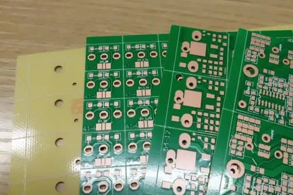
China’s vast manufacturing sector has fostered the growth of a comprehensive supply chain for PCB production. Core materials such as FR4 (the most common base material for PCBs), copper foils, and various laminates are readily available locally. This local availability eliminates the need for costly imports and reduces transportation expenses.

2.2 Vertical Integration of Supply Chains

Many Chinese PCB manufacturers have adopted a vertically integrated business model. This means they not only produce PCBs but also manufacture or source key components and materials within their own network. Such integration allows for better control over costs and quality, leading to more competitive pricing.

2.3 Lower Material Transportation Costs Within China

The strategic location of PCB factories near raw material suppliers significantly reduces transportation costs. The well-developed transportation infrastructure within China’s manufacturing hubs further enhances this advantage, allowing for quick and cost-effective movement of materials and finished products.

Read more about:

3. Advanced Manufacturing Technology and Automation

3.1 Investment in Modern PCB Manufacturing Equipment

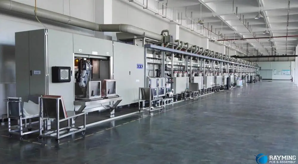
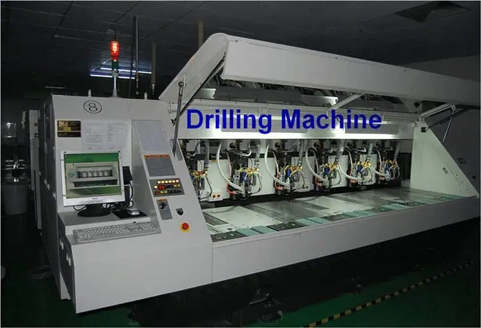
Chinese PCB manufacturers have made substantial investments in state-of-the-art manufacturing equipment. Advanced technologies such as CNC drilling machines, laser cutting systems, and Automated Optical Inspection (AOI) systems have become standard in many Chinese factories. These technologies not only improve precision and quality but also increase production efficiency, thereby reducing costs.

3.2 High Throughput Production Lines

The implementation of high-throughput production lines in Chinese PCB factories has dramatically increased production speed and efficiency. Automated systems handle various aspects of PCB production, from material handling to testing, minimizing human error and reducing labor costs.

3.3 PCB Manufacturing Machine Costs in China

Interestingly, the cost of PCB manufacturing equipment in China is often lower than in other countries. This is partly due to local production of such machinery and partly due to government incentives for upgrading manufacturing technology. Lower equipment costs translate to lower overhead for manufacturers, contributing to the overall low cost of PCBs.

4. Government Policies and Industrial Support

4.1 Incentives and Subsidies for Electronics Manufacturing

The Chinese government has long recognized the importance of the electronics manufacturing sector and has implemented various policies to support its growth. These include tax incentives, subsidies for research and development, and financial support for companies investing in advanced technologies.

4.2 Infrastructure Development

Significant investments in infrastructure, including modern ports, efficient road networks, and reliable power supply, have greatly benefited the PCB industry. This well-developed infrastructure reduces logistical costs and improves overall operational efficiency.

4.3 Export-Friendly Trade Policies

China’s export-oriented policies have created a favorable environment for PCB manufacturers to sell their products globally. Various trade agreements and export incentives have made it easier and more cost-effective for Chinese companies to reach international markets.

5. Lower Labor Costs Compared to Other Countries

5.1 Skilled but Cost-Effective Workforce

While labor costs in China have been rising in recent years, they remain significantly lower than in many developed countries. The PCB industry in China benefits from a large pool of skilled workers who are proficient in various aspects of PCB manufacturing, yet command wages that are competitive on a global scale.

5.2 Specialized Training Programs

Many regions in China have implemented specialized training programs focused on PCB assembly and testing. These programs ensure a steady supply of skilled workers, reducing training costs for manufacturers and maintaining a high level of expertise in the workforce.

5.3 Labor Cost Comparison

When compared to countries like the USA, Japan, or those in Europe, China’s labor costs in the PCB industry can be 50-70% lower. This significant difference in labor expenses plays a crucial role in keeping overall production costs down.

6. Highly Competitive Domestic Market

6.1 Intense Competition Among PCB Manufacturers

The PCB industry in China is characterized by intense competition among numerous manufacturers. This competitive environment leads to continuous price wars, forcing companies to optimize their processes and reduce costs to remain viable. While challenging for the manufacturers, this competition ultimately benefits customers through lower prices.

6.2 Impact of Competition on Innovation and Efficiency

The fierce competition in China’s PCB market has spurred innovation and efficiency improvements. Manufacturers constantly seek ways to streamline their processes, reduce turnaround times, and offer value-added services like rapid prototyping. This drive for efficiency further contributes to cost reduction and improved service quality.

7. Specialization in Different PCB Types

7.1 Standard PCB vs. Custom PCB Manufacturing

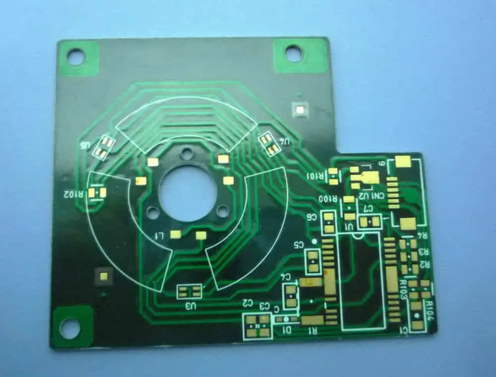
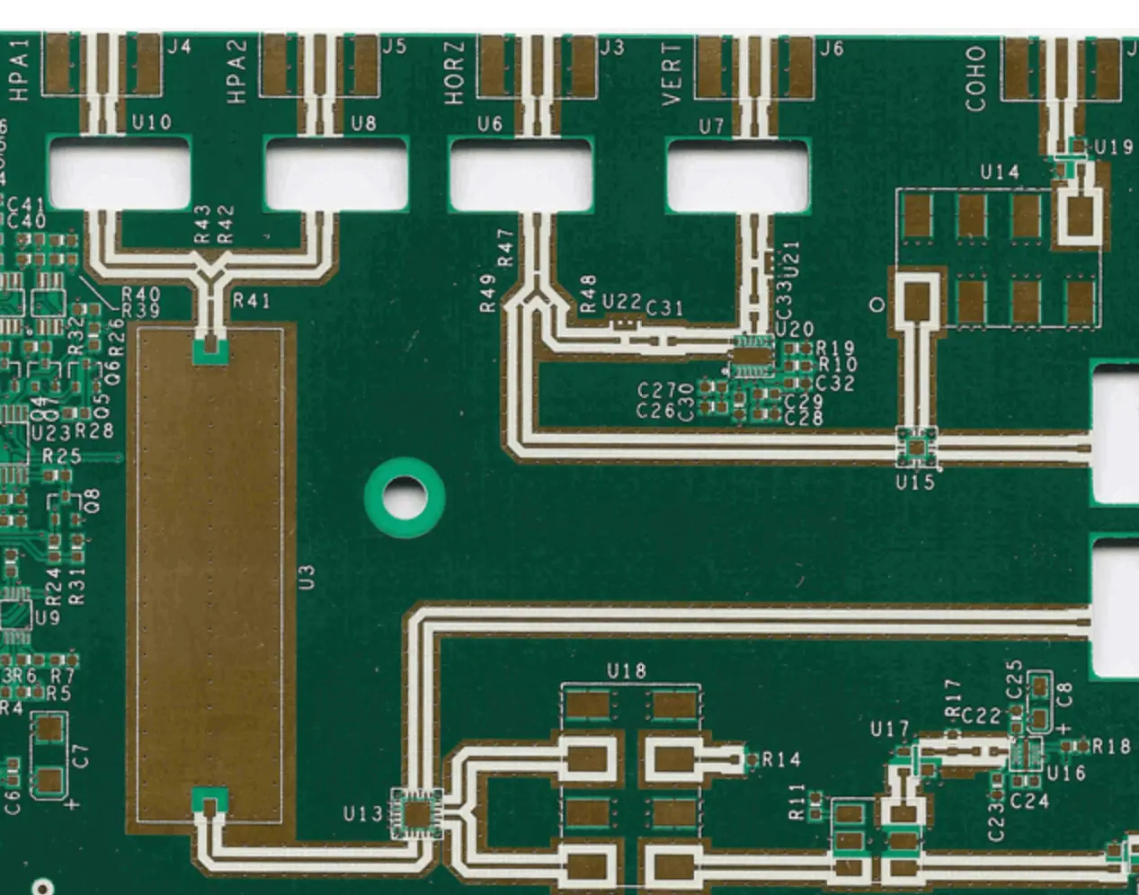
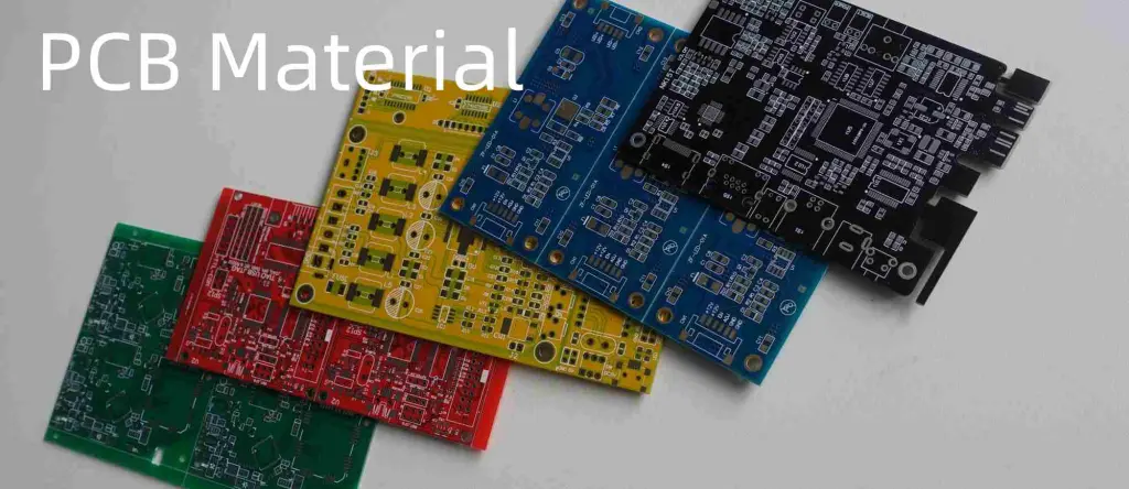
Chinese manufacturers have become highly efficient in producing standard PCBs, such as 2-layer and 4-layer boards. The streamlined processes for these common configurations allow for faster production and lower costs. However, many Chinese manufacturers also excel in custom PCB production, offering competitive prices for specialized designs.

7.2 Diverse PCB Offerings at Low Prices

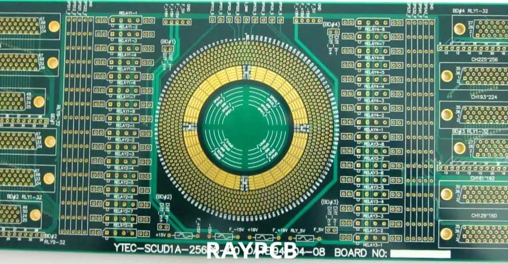
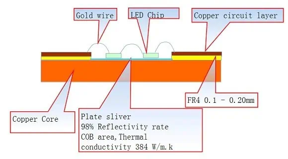
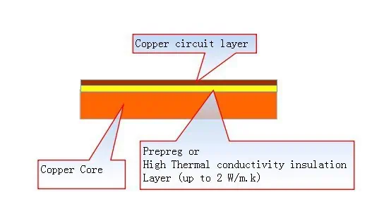
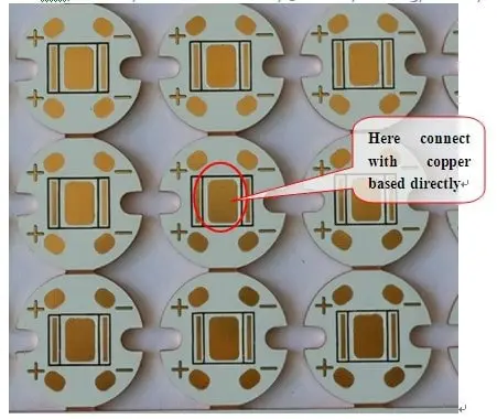
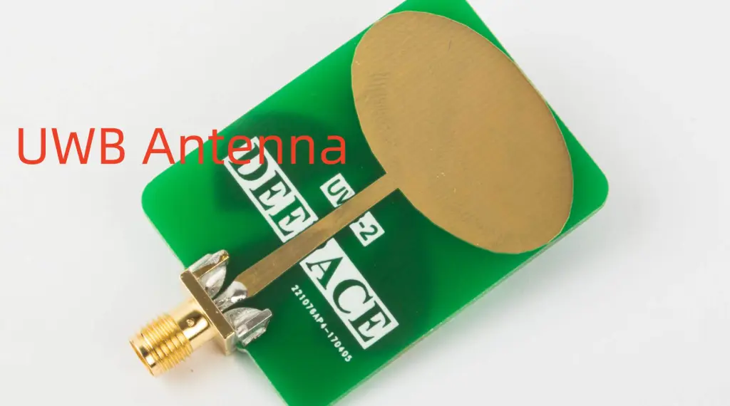
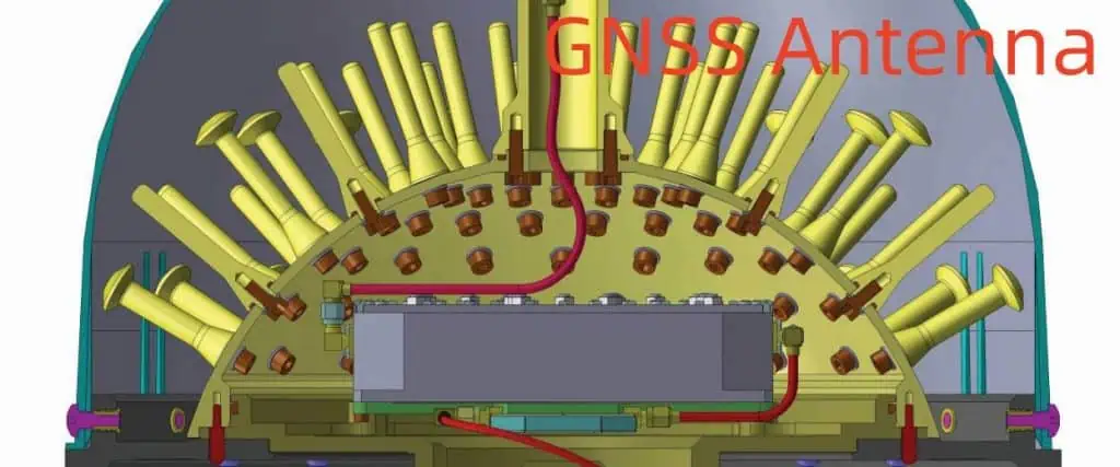
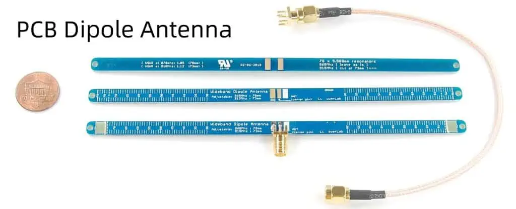
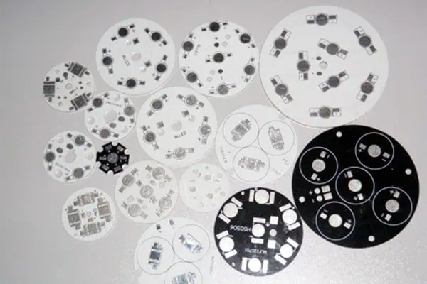
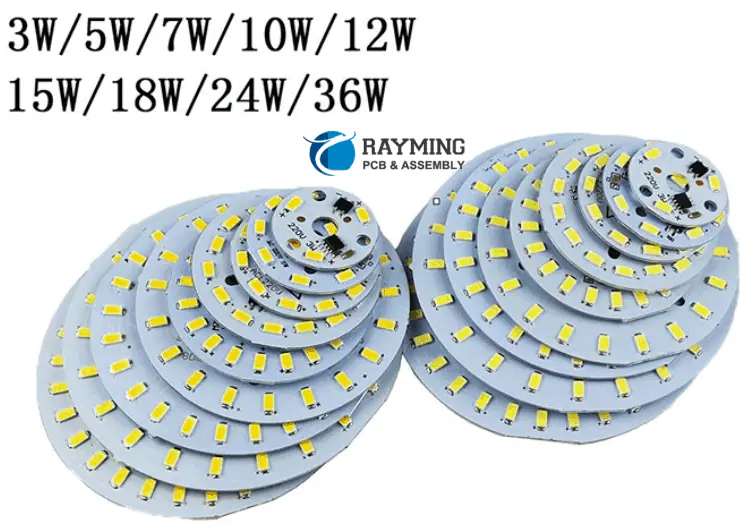
The specialization extends to various PCB types, including flexible PCBs, LED PCBs, and amplifier PCBs. By focusing on specific niches, manufacturers can optimize their processes and offer these specialized products at surprisingly low prices. This specialization allows for economies of scale even in more complex PCB types.

8. Efficient Logistics and Global Shipping

8.1 Strategic Location of PCB Factories

Many PCB factories in China are strategically located near major ports and transportation hubs. This proximity reduces domestic transportation costs and facilitates quick and easy shipping to international markets.

8.2 Partnered Logistics Companies

Chinese PCB manufacturers often have partnerships with logistics companies that offer competitive shipping rates. These partnerships, combined with the high volume of shipments, allow for significant cost savings in international shipping.

8.3 Role of Online PCB Services

Companies like PCBWay and JLCPCB have revolutionized the global distribution of PCBs from China. These online platforms offer user-friendly interfaces for ordering custom PCBs, provide instant quotes, and manage the complexities of international shipping, making it easier than ever for global customers to access low-cost Chinese PCBs.

9. Common Misconceptions About Cheap China PCBs

9.1 Is Lower Price Equal to Lower Quality?

A common misconception is that low-cost PCBs from China are of inferior quality. While it’s true that some low-end manufacturers may cut corners, many Chinese PCB manufacturers produce high-quality boards that meet or exceed international standards. The key is to choose reputable suppliers with proper certifications and quality control processes.

9.2 Risks to Watch Out For

While the Chinese PCB market offers excellent opportunities for cost savings, buyers should be aware of potential risks. These include the possibility of counterfeit components in some supply chains and inconsistent quality from less reputable manufacturers. Due diligence in supplier selection is crucial to mitigate these risks.

10. How to Leverage China’s PCB Market Effectively

10.1 Tips for Choosing a Good Manufacturer

When selecting a Chinese PCB manufacturer, consider the following:

  • Look for relevant certifications (ISO 9001, UL, RoHS, etc.)
  • Check customer reviews and testimonials
  • Verify their testing standards and quality control processes
  • Request samples before placing large orders
  • Assess their communication responsiveness and English proficiency

10.2 Balancing Cost, Quality, and Lead Time

While low cost is attractive, it’s important to balance it with quality requirements and lead times. Sometimes, paying a slightly higher price can result in better quality, more reliable delivery, or enhanced customer service, which can save money and headaches in the long run.

Conclusion

The low cost of China PCB circuit boards is the result of a complex interplay of factors, including economies of scale, advanced manufacturing technologies, lower labor and material costs, government support, and intense market competition. These elements combine to create an environment where high-quality PCBs can be produced at remarkably low prices.

For startups and established companies alike, China remains a smart choice for PCB sourcing. The country’s PCB industry offers a compelling combination of cost-effectiveness, quality, and production capacity that is hard to match elsewhere in the world.

However, it’s crucial to approach PCB sourcing from China with due diligence. By carefully selecting manufacturers, understanding the market dynamics, and balancing cost considerations with quality requirements, businesses can fully leverage the advantages of China’s PCB industry while mitigating potential risks.

As the global electronics industry continues to evolve, China’s position as a leader in low-cost, high-quality PCB manufacturing seems secure for the foreseeable future. Whether you’re working on a small prototype or planning large-scale production, China’s PCB industry offers solutions that can significantly impact your project’s success and bottom line.

Why Is Cem-1 PCB Material still Popular in the Circuit Board Market ?

cem 1 pcb circuit board

Cem-1 PCB material ?   

Is so strange for the most of people ,  is one of Base Material for printed circuit boards. Is low grade in the PCB material industry , Only for Single side PCB, But it is used very widely .

Some People will say  Now Technology  develop so fast , Every Electronic device become smaller and thinner . Why so low grade material can be use widely .

Is true , Technology is becoming higher and higher , but mean time , Components is also high assemblied more function , This will let more designer use single side PCB ( Cem-1 Material ) to control their Cost .

Single Side PCB ( One Layer PCB )  will reduce the design cost very much , thatโ€™s the most important reason .

Cem-1 Material

CEM 1 PCB
CEM 1 PCB

he materials suitable under the CEM-1 specification in classification of NEMA โ€“ the most widespread materials for production of 1-layers printed circuit boards.

Standard CEM-1 material is composite material on a cellulose basis with one layer of glass fibre laminate (FR-4) on a surface. Usually CEM-1 has milky-white color.

The feature of this material is the impossibility of realization the metallization through holes, thus, this material can be used only for production of 1-layer printed-circuit boards.

Standard CEM-1 satisfies to combustibility class UL 94-V0, as FR-4 material. Mechanical characteristics of CEM-1 are little bit worse, than at FR-4: CEM-1 is more fragile. The dielectric constant and a tangent of angle of dielectric losses of both materials are differ insignificantly.

Thus, CEM-1 is a cheaper alternative for FR-4 material for production of 1-laye prototype printed-circuit boards.

CEM-1 PCB Material Technical parameters

In Cem PCB Material Family  ,Have other better one CEM-3 ,    Letโ€™s see the difference CEM-1 and CEM -3

FULL PCB MANUFACTURING Quote

CEM-1 Composite material composed of woven glass fabric surfaces and paper core combined with epoxy resin. Primarily used in the printed circuit board industry. Easy punching and excellent electrical properties and higher flexural strength than paper based grades. CEM-1 provides excellent mechanical and electrical properties, and punches well up to .093โ€ณ.

CEM-3 is very similar to FR4. Instead of woven glass fabric a โ€˜fliesโ€™ type is used. CEM-3 has a milky white color and is very smooth. It is a complete replacement for FR4 and has a very large market share in Asia. It is a kind of flame retardant epoxy copper-clad plate glass material, is generally used in electronics with double sided and multilayer pcb boards. And CEM โ€“ 3 is a new printed circuit substrate material developed based on FR โ€“ 4. In recent years, CEM-3 is used to replace FR-4 in Japan, even more than the FR โ€“ 4 dosage.

In Led lighting Market ,Most of Led PCB Manufacturer  use Cem1 as base Material . it can give the best balance between The heat dissipating performance and PCB cost .

In Next article we will introduce more low grade PCB material  for our electronic designer , give a low Cost PCB solution to you .

Fr1 . FR2 , FR3, 22F, CEM 1 ,Cem 3 . FR4, FR5,   Whatโ€™s difference between them ? How to Choose the suitable material for your design?  how to control your PCB cost , Let โ€˜s wait the next article coming .

16 Q&A – How to Choose a manufacturer for PCB hobbyist?

printed circuit board manufacturers

Introduction

Printed circuit boards (PCBs) form the core of an electronics hobbyistโ€™s projects. For professional looking, functional boards that bring your design ideas to life, choosing the right PCB manufacturer is key. This article covers the key factors to consider when selecting a PCB fabrication partner as an electronics hobbyist through 16 commonly asked questions:

Q1. What volume of PCBs do I need as a hobbyist?

For hobbyists and makers, the typical quantity of boards required for a project is usually quite low – ranging from just 1-2 prototype boards for testing up to about 50-100 boards for small scale building. This is considered low volume in PCB fabrication. So look for manufacturers that can support prototyping and small batch orders.

Q2. What size of PCBs will I need?

Typical PCB sizes in hobbyist projects range from 10mm x 10mm boards for tiny circuits to about 200mm x 100mm for more complex projects. Maximum sizes can go up to 300mm x 300mm but usually not larger. Select a vendor that can fabricate boards in this range of compact sizes.

Q3. What PCB technology choices do I have?

Hobbyist boards are typically 2 layer or 4 layer designs using standard FR-4 material. Some projects may need 6 layers or flex PCBs. Ensure your vendor can handle layer counts from 1 to 6, different dielectric materials, trace/space down to 5 mil, plated slots/holes, gold plating, carbon printing etc.

Q4. What budget should I allocate for PCB fabrication?

LPI PCB
LPI PCB

For prototype 2 layer boards of 50mmx50mm size, expect costs of around $5 to $10 per piece for 10-piece quantity from China. For larger 4 layer boards up to 200x200mm in 10-pc quantity, costs are approximately $50-100 per board. Budget 1.5 to 2 times more for very quick turnaround.

Q5. What are the PCB fabrication process capabilities needed?

Look for suppliers offering: solder mask, silkscreen legend, controlled impedance, HAL, minimum hole sizes of 0.2mm, copper thickness up to 2 oz., Underwriters Lab (UL) approval, RoHS compliance and lead-free processing. Not all of these may be needed but having these capabilities ensures your supplier can meet future needs as projects increase in complexity.

Q6. How do I check the reliability and quality of the PCB manufacturer?

Ask about their quality certifications like ISO 9001. Review online testimonials and feedback on forums. Evaluation samples from potential vendors. Ask detailed questions on their quality assurance practices. A reliable manufacturer will be transparent and even allow site visits.

Q7. What special services do I need as a hobbyist?

Hobbyists need:

  • Low NRE (non-recurring engineering) charges or none for complex designs
  • No minimum order quantity – ability to order single pieces
  • Quickturn fabrication in 3-5 days to test designs faster
  • Basic assembly services to get ready boards
  • Virtual communication for design reviews

Q8. What support for design is important?

Design support services that help hobbyists include:

  • Online quotes based on your uploaded Gerber files
  • Free DFM (design for manufacturing) analysis to check your design against fab norms
  • Quick online communication for design reviews
  • Prototype PCB fabrication in 24-48 hours
  • Supplying required design libraries and templates

Q9. How do I assess technical capabilities of a PCB manufacturer?

Review their technology roadmap and offerings vs industry standards to assess technical competence – things like line/space capabilities, microvia sizes, impedance control tolerances, HDI stacking abilities etc. The right partner for an advanced hobbyist should have strong technical expertise.

Q10. What certifications should I look for in a PCB supplier?

Relevant quality and sustainability certifications include:

  • ISO 9001 or AS9100 – Quality management
  • ISO 14001 – Environmental
  • IATF 16949 – Automotive quality
  • UL – Product safety testing
  • RoHS – Hazardous substances process control
  • IPC standards – PCB manufacturing

Q11. How important are environmental factors in choosing a PCB supplier?

As a hobbyist, ensuring your PCB manufacturer follows environmental rules on wastewater treatment, emissions norms, chemical handling etc. promotes sustainability. They should be REACH and RoHS compliant. If they have ISO 14001 certification, even better.

Q12. Does manufacturer location matter for a hobbyist?

Location has a major impact on cost, lead time and communication access for on-demand prototyping needs. For fastest turnaround and cost savings, use manufacturers based in China. But also consider your intellectual property security when sharing design information.

Q13. How do I evaluate potential PCB manufacturers before selecting one?

Ways to evaluate suppliers:

  • Get free design review and quotation
  • Review online reputation and testimonials
  • Assess responsiveness of sales and engineering team
  • Ask for samples of similar PCBs built recently
  • Validate quality certifications and technical expertise

Q14. What questions should I ask PCB manufacturer before ordering?

PCB drilling machine

Important questions hobbyists should clarify:

  • What are your capabilities in PCB fabrication and assembly?
  • What engineering support do you provide during design?
  • What design standards do you follow?
  • What quality control checks are performed during manufacturing?
  • How do you ensure protection of my IP/design data?
  • What certifications have you obtained?
  • Do you have liability insurance to cover defects?

Q15. What are signs of a good PCB manufacturer for prototype projects?

Characteristics of a good prototyping partner:

  • No minimum order quantity
  • Quickturn fabrication in 3-5 days
  • Low NRE (non-recurring engineering) charges
  • Willingness to fabricate low volumes
  • Capability to scale to medium volumes
  • Good design and engineering support
  • Quality and reliability focused

Q16. What mistakes should I avoid when choosing a PCB supplier as a hobbyist?

Common mistakes to avoid:

  • Selecting purely based on lowest price quotes -Going with unknown, new companies without reputation
  • Assuming overseas companies have lower quality
  • Not checking their qualifications and certifications
  • Not reviewing prototypes before larger builds
  • Not having a robust manufacturing agreement

Conclusion

Choosing the right PCB manufacturing partner is key to ensuring success as an electronics hobbyist. Evaluating suppliers based on capabilities, services, quality, responsiveness, and costs helps identify the best prototyping partner for your unique needs. With the right selection, hobbyists can fully realize their PCB designs and product ideas.

Key Takeaways

  • Focus on manufacturers equipped for low volume prototyping
  • Leverage design support services like DFM analysis
  • Prioritize quality, reliability and technical capabilities
  • Evaluate based on certifications, customer reviews and pre-production sampling
  • Analyze total costs not just unit prices
  • Align supplier location and capabilities with target lead times
  • Establish effective communication channels and IP protection

Recommendations

Reliable PCB suppliers with strong support for hobbyist prototyping include:

  • Rayming Technology- China based, excellent engineering support
  • Seeed Studio – China, community marketplace and Fusion PCB service
  • JLCPCB – China, very fast delivery at low cost
  • OSH Park – US based, small batches with quickturn
  • Eurocircuits – Europe, proven quality and 25+ years experience

With the right partner, hobbyists can take their electronics projects from concept to reality smoothly.

How to Choose the Right LED Chips for Lighting Design

Introduction

LED lighting is fast replacing traditional incandescent and fluorescent lighting due to benefits like high energy efficiency, long life and design flexibility. At the heart of an LED lighting product are the LED chips which provide the illumination. Choosing the right LED chips is crucial for achieving the target light output, efficiency, color characteristics and reliability.

This article discusses how to select appropriate LED chips for lighting design including parameters like power, luminous efficacy, color temperature, CRI index and thermal management. Read on for practical guidance to pick optimal LEDs for your lighting application.

Key LED Chip Specifications

The main parameters that characterize an LED chip are:

Power Rating

  • Measured in Watts
  • Determines light output
  • Options range from 0.2W to over 10W

Forward Voltage

  • Typical values between 2V to 4V
  • Impacts the driver design

Luminous Efficacy

  • Measure of light output vs input power
  • Given in lumens/Watt (lm/W)
  • Higher is more energy efficient

Peak Wavelength

  • Determines color – 620-630nm is red, 520-535nm is green etc.
  • For white LEDs, blue chip + yellow phosphor is common

Color Temperature

  • Warm white, neutral or cool white
  • Measured in Kelvin (K)
  • 2700-3000K is warm white, 5000-6000K is cool white

CRI Index

  • Color Rendering Index
  • Rating of color quality – maximum of 100
  • Higher CRI gives better light quality

Viewing Angle

  • Beam width at 50% intensity points
  • Narrow (15ยฐ), medium (25-50ยฐ) or wide (120ยฐ+) available

Lifetime

  • Hours of operation before light output declines by 30%
  • 30,000 to 100,000 hour lifetimes are common

Package Type

  • Surface mount or through-hole LEDs
  • Defines how it’s soldered to PCBs

Key Considerations for LED Chip Selection

Primary aspects to consider when choosing LED chips for lighting include:

Target Luminosity

  • How much visible light is needed for the application?
  • Select chips with lumen output in required range

Efficiency

  • Higher lumens/watt improves energy efficiency
  • Balances luminosity vs power consumption

Color Temperature

  • Depends on lighting ambiance needed
  • Warm, neutral or cool white?

Color Quality

  • Higher CRI gives better light quality
  • CRI 80+ is desirable for most lighting

Operating Life

  • Lifetime of LED chips should match product life
  • Select chips with 50,000 hours or greater lifetime

Thermal Management

  • LEDs produce heat which impacts performance
  • Ensure ambient temperatures are within chip rating

Driver Interface

  • Forward voltage and constant current needs
  • Match to chosen LED driver design

Physical Size

  • Overall dimensions and pad spacing
  • Ensure PCB layout accommodates chip package

Budget

  • Balance performance vs unit cost of LED chips

Let’s look at some of these aspects in more detail.

LED Chip Power Ratings

Available LED chip power ratings include:

  • Low power: 0.2W to 0.5W
  • Medium power: 1W to 3W
  • High power: 5W to 10W

Higher power LEDs produce greater luminous output. But the increased heat needs thermal management.

For most general lighting like bulbs, downlights and strips, mid-power 1W to 3W LED chips offer a good compromise between light output and easier thermal control vs high power chips.

But specialty lighting like high bay lighting may use higher 5W-10W LEDs. While battery powered flashlights can use tiny 0.2W-0.5W chips.

Lumen Output

The lumen rating of LED chips depends on the power and efficacy. Various luminosity bins are available for each LED chip ranging from low to high lumens.

Typical lumen output for various power LEDs:

  • 1W LED chip – 100 to 130 lumens
  • 3W LED chip – 250 to 300 lumens
  • 5W LED chip – 400 to 500 lumens
  • 10W LED chip – 900 to 1000 lumens

Select chips with lumen output that meet the application’s illumination needs. Combine multiple lower lumen LEDs for higher brightness.

LED Chip Efficacy

Higher efficacy or lumens/watt improves lighting energy efficiency. LED chip efficacy has increased enormously over the years due to technology improvements.

  • Older LED chips had efficacy of 30-60 lm/W
  • Mid-power modern LEDs now achieve up to 90-120 lm/W
  • High power LEDs range from 100-150 lm/W

For a given power rating, choose LED chips with the highest efficacy within budget. This maximizes light output vs power consumption.

Color Temperature

LED Aluminum Substrate

Color temperature determines the visual color tone of white light – from warm white to cool white.

Common white LED color temperatures:

  • Warm white: 2700K to 3000K
  • Neutral white: 3500K to 4100K
  • Cool white: 5000K to 6500K

Warm white is commonly used in homes for cozy lighting. Cool white is preferred where brighter illumination is needed. Select color temperature depending on lighting ambiance needed.

CRI Index

The Color Rendering Index (CRI) indicates how accurately colors are displayed in the light.

  • Low CRI like 70-75 gives poor color
  • Medium CRI of 80-90 is generally acceptable
  • High CRI > 90 approximates natural light

Aim for LED chips delivering 80+ CRI for quality lighting applications. chips with CRI 90+ can provide near natural color rendition.

LED Chip Lifetime

LED chips last much longer than traditional light sources. But over time, light output gradually declines due to phosphor degradation.

  • 30,000 hours is minimum lifetime needed
  • 50,000 hours is typical for quality mid-power LED chips
  • 100,000 hours lifetime LEDs are used for extra reliability

Match the LED chip operating life to the target product lifespan. Also factor in ambient temperature which affects LED lifetime.

Thermal Management

LED chips generate significant heat. Operating at high temperatures lowers light output and shortens lifetime. Effective thermal management is vital.

  • Use quality aluminum PCBs or ceramic substrates to conduct heat away from the LED chips.
  • Thermal interface materials like epoxy or grease improve heat transfer to the board.
  • Ensure ambient air temperature around LEDs stays within recommended range.
  • Allow spacing between LEDs for airflow to limit temperature rise.

Proper thermal design greatly improves LED chip performance and longevity.

LED Chip Packages

LED SMT

Common LED chip package types include:

  • SMD – Low profile surface mount devices, easy to solder
  • COB – Chip on board arrays, combine multiple LEDs
  • Through-hole – Used for screw based bulbs
  • Ceramic substrates – Provide electrical isolation

SMD packages allow easier PCB assembly while COB arrays simplify optics design. Consider package height restrictions and soldering processes when selecting.

Conclusion

Choosing optimal LED chips by carefully evaluating key parameters like power rating, luminosity, efficiency, color characteristics, lifetime and thermal management enables creating energy-efficient, long lasting and good quality lighting products. Leverage the latest mid-power and high-power LED chips to realize substantial energy savings and simplified lighting design. With technology advancements delivering ever more performant LED chips, lighting product developers can take advantage by selecting the most appropriate chips to meet their precise application needs.

FAQs

What are the main differences between mid-power and high-power LED chips?

Mid-power LEDs (1-3W) strike a balance between light output and easier thermal management. High-power LEDs (5-10W) produce higher brightness but require substantial heat sinking.

How important is the PCB design for an LED lighting product?

Proper PCB thermal management through large copper planes, thermal vias, airflow and heat sinks is crucial to ensure LED chips operate at optimal temperature for maximum light output and reliability.

What causes LED chips to degrade over their lifetime?

Operating LED chips at high junction temperatures accelerates luminous decay, color shift and failures over time. Quality encapsulation also protects against moisture ingress and corrosion.

Can the color temperature of white LEDs shift over their lifetime?

Yes, white LEDs can gradually shift to a bluer tone over tens of thousands of hours of use. Higher quality LED chips exhibit better color consistency throughout their lifetime.

How does photon efficiency relate to LED efficacy?

Photon or wall-plug efficiency defines the LED chip’s inherent ability to convert electrons to photons. Maximizing this improves luminous efficacy (lumens per watt). Chip design, materials and packaging maximize photon efficiency.

Complete PCB Stackup Guide: Standard 4/6/8 Layers, Flex, Rigid-Flex & Manufacturer Comparisons

multilayer pcb stackup

Introduction

In the ever-evolving world of electronics, Printed Circuit Boards (PCBs) serve as the backbone of nearly every device we use. At the heart of PCB design lies a crucial concept known as PCB stackup. Whether you’re a seasoned engineer or a budding electronics enthusiast, understanding PCB stackup is essential for creating efficient, reliable, and high-performing circuit boards.

What is a PCB Stackup?

A PCB stackup refers to the arrangement of copper layers, prepreg, and core materials that make up a printed circuit board. It defines the number of layers, their order, thickness, and the materials used between them. This configuration plays a pivotal role in determining the board’s electrical, mechanical, and thermal properties.

Importance of Proper PCB Stackup in Design and Manufacturing

The importance of a well-designed PCB stackup cannot be overstated. It directly impacts:

  1. Signal Integrity: Proper stackup minimizes crosstalk and EMI, ensuring clean signal transmission.
  2. Power Distribution: Effective power and ground plane placement for optimal power delivery.
  3. Thermal Management: Influences heat dissipation throughout the board.
  4. Manufacturing Yield: A well-planned stackup improves manufacturability and reduces defects.
  5. Cost Efficiency: Optimized stackups can reduce material usage and production costs.

Brief Overview: 4/6/8 Layers, Flex, Rigid-Flex

This comprehensive guide will delve into various PCB stackup configurations, including:

  • Standard multilayer PCBs: 4-layer, 6-layer, and 8-layer designs
  • Flexible PCB: Single and multi-layer flex circuits
  • Rigid Flex PCB: Hybrid designs combining rigid and flexible sections

We’ll explore the unique characteristics, advantages, and applications of each type, providing you with the knowledge to choose the right stackup for your project.

1. Understanding PCB Stackup Basics

Definition of PCB Stackup

A PCB stackup is the cross-sectional view of a printed circuit board that details the number, order, and composition of layers. It’s essentially the blueprint of how the PCB is constructed, layer by layer.

Role of Layer Stackup in PCB Performance

The layer stackup directly influences several key aspects of PCB performance:

  1. Electrical Performance: Affects impedance control, signal integrity, and EMI shielding.
  2. Mechanical Stability: Determines the board’s physical strength and resistance to warping.
  3. Thermal Management: Influences heat distribution and dissipation.
  4. Reliability: Proper stackup design can enhance the long-term reliability of the PCB.

Key Elements: Layers, Materials, Dielectric, Copper Weight, Prepreg, Core

To fully grasp PCB stackup, it’s crucial to understand its key components:

  1. Layers: Copper layers where circuits are etched.
  2. Materials: Substrates like FR-4, Rogers, or polyimide.
  3. Dielectric: Insulating material between conductive layers.
  4. Copper Weight: Thickness of copper foil, measured in ounces per square foot.
  5. Prepreg: Pre-impregnated bonding material used to join layers.
  6. Core: A more rigid, cured material that provides structural support.

Common Applications for Multilayer PCBs

Multilayer PCBs find applications across various industries due to their versatility and performance benefits:

  • Consumer Electronics: Smartphones, laptops, smart home devices
  • Automotive: Engine control units, infotainment systems, safety features
  • Aerospace: Avionics, satellite communications
  • Medical Devices: Diagnostic equipment, implantable devices
  • Industrial Controls: Factory automation, robotics
  • Telecommunications: Network routers, 5G infrastructure

Read more about:

2. Standard PCB Stackups: 4, 6, and 8 Layers

2.1 4-Layer PCB Stackup

Typical Layer Arrangement

A standard 4-layer PCB stackup usually consists of:

  1. Top Signal Layer
  2. Ground Plane
  3. Power Plane
  4. Bottom Signal Layer

This arrangement provides a balance between cost and performance for many applications.

Signal Integrity, EMI Shielding, Power/Ground Planes

  • Signal Integrity: The ground and power planes sandwiched between signal layers help reduce crosstalk and improve signal quality.
  • EMI Shielding: The internal planes act as shields, reducing electromagnetic interference.
  • Power/Ground Planes: Dedicated layers for power distribution ensure stable voltage supply and low impedance return paths.

Ideal Use Cases and Industries

4 layer PCBs are widely used in:

  • Consumer electronics (e.g., digital cameras, smart home devices)
  • Automotive electronics (e.g., sensor modules, control units)
  • Industrial controls (e.g., PLC modules, HMI interfaces)
  • IoT devices (e.g., smart sensors, wearables)

2.2 6-Layer PCB Stackup

Layer Structure Examples

A common 6 layer PCB stackup might include:

  1. Top Signal Layer
  2. Ground Plane
  3. Signal Layer
  4. Power Plane
  5. Signal Layer
  6. Bottom Ground Plane

This configuration offers more flexibility in routing and improved signal integrity compared to 4-layer designs.

Benefits over 4-Layer (Better EMI, Routing Density)

  • Enhanced EMI Shielding: Additional ground layers provide better electromagnetic shielding.
  • Increased Routing Density: More signal layers allow for complex routing in a compact space.
  • Improved Signal Integrity: Better separation of high-speed signals from power/ground planes.
  • Enhanced Power Distribution: Dedicated power and ground planes for cleaner power delivery.

Applications Needing High-Speed, Low Noise

6-layer PCBs are ideal for:

  • High-speed digital circuits (e.g., high-performance computing)
  • Analog/mixed-signal designs (e.g., data acquisition systems)
  • RF and microwave applications (e.g., wireless communication modules)
  • Medical imaging equipment

2.3 8-Layer PCB Stackup

Standard Stackup Configurations

An 8 layer PCB stackup might be arranged as follows:

  1. Top Signal Layer
  2. Ground Plane
  3. Signal Layer
  4. Power Plane
  5. Ground Plane
  6. Signal Layer
  7. Ground Plane
  8. Bottom Signal Layer

This configuration offers maximum flexibility and performance for complex designs.

High-Speed Design Requirements

8-layer PCBs are often necessary for high-speed designs due to:

  • Improved Signal Isolation: Multiple ground planes minimize crosstalk.
  • Enhanced Power Distribution: Dedicated power planes for different voltage requirements.
  • Better Impedance Control: More options for controlling trace impedance.
  • Reduced EMI: Multiple shielding layers for superior EMI performance.

Challenges and Solutions in 8-Layer Design

Challenges:

  • Increased complexity in design and manufacturing
  • Higher material costs
  • Potential for increased thermal issues due to more layers

Solutions:

  • Advanced PCB design software for complex stackup planning
  • Careful thermal management techniques (e.g., thermal vias, copper pours)
  • Collaboration with manufacturers to optimize for cost and performance

3. Advanced Stackup Types: Flex and Rigid-Flex PCBs

3.1 Flexible PCB Stackup

Flex PCB Layer Structures

Flexible PCBs can range from single-layer to multi-layer designs:

  1. Single-Layer Flex: One conductive layer on a flexible substrate
  2. Double-Layer Flex: Two conductive layers with a flexible core
  3. Multi-Layer Flex: Multiple conductive layers separated by flexible dielectric materials

Materials (Polyimide, Adhesiveless, etc.)

Common materials used in flex PCB stackups include:

  • Polyimide: Offers excellent flexibility and heat resistance
  • Adhesiveless Materials: Provide better flex life and dimensional stability
  • Liquid Crystal Polymer (LCP): Suitable for high-frequency applications
  • PTFE-based Materials: Used for high-speed, low-loss designs

Unique Challenges: Bending Radius, Layer Integrity

Flex PCBs face unique challenges:

  • Bending Radius: Ensuring the PCB can bend without damaging traces or components
  • Layer Integrity: Maintaining connections between layers during flexing
  • Material Selection: Choosing materials that can withstand repeated bending
  • Component Placement: Strategically placing components to minimize stress on solder joints

Typical Applications (Wearables, Aerospace)

Flex PCBs are commonly used in:

  • Wearable Technology: Fitness trackers, smart clothing
  • Aerospace: Satellite systems, aircraft control panels
  • Medical Devices: Implantable electronics, hearing aids
  • Automotive: Dashboard displays, steering wheel controls
  • Consumer Electronics: Smartphone internal connections, camera modules

3.2 Rigid-Flex PCB Stackup

Hybrid Structures: Rigid + Flex

Rigid-flex PCBs combine rigid and flexible sections in a single board:

  • Rigid Sections: Multi-layer stackups similar to standard PCBs
  • Flex Sections: Single or multi-layer flexible circuits
  • Transition Zones: Areas where rigid and flex sections connect

Stackup Planning for Dynamic Flexing

Considerations for rigid-flex stackup design include:

  • Neutral Bend Axis: Positioning signal layers near the center of the flex section
  • Adhesiveless Construction: Using adhesiveless materials in flex areas for better performance
  • Copper Thickness: Balancing copper weight for flexibility and durability
  • Layer Symmetry: Ensuring balanced construction to prevent warping

Cost vs. Benefit Considerations

Rigid-flex PCBs offer several benefits but at a higher cost:

Benefits:

  • Space savings by eliminating connectors
  • Increased reliability due to fewer interconnections
  • Design flexibility for complex 3D applications

Costs:

  • Higher material and manufacturing costs
  • More complex design process
  • Specialized manufacturing capabilities required

Common Use Cases

Rigid-flex PCBs are ideal for:

  • Military and Aerospace: Compact, reliable electronics for harsh environments
  • Medical Devices: Space-constrained applications like pacemakers or endoscopes
  • Consumer Electronics: Foldable smartphones, laptop hinges
  • Automotive: Instrument clusters, infotainment systems
  • Industrial Equipment: Robotic arms, rotating or moving assemblies

4. Key Considerations When Designing PCB Stackups

Impedance Control and Signal Integrity

Proper impedance control is crucial for maintaining signal integrity:

  • Trace Width and Spacing: Calculate based on desired impedance and layer thickness
  • Reference Planes: Ensure consistent reference planes for high-speed signals
  • Layer Ordering: Place high-speed signals adjacent to uninterrupted reference planes
  • Differential Pair Routing: Maintain consistent spacing and length matching

Power Delivery and Grounding Strategies

Effective power distribution is essential for PCB performance:

  • Plane Layer Allocation: Dedicate layers for power and ground planes
  • Split Planes: Use split planes for multiple voltage requirements
  • Decoupling Capacitors: Proper placement and selection of decoupling capacitors
  • Return Path Planning: Ensure low-impedance return paths for all signals

Thermal Management

Consider thermal aspects in stackup design:

  • Copper Weight: Heavier copper for improved heat dissipation
  • Thermal Vias: Strategically placed vias to conduct heat between layers
  • Material Selection: Choose materials with appropriate thermal conductivity
  • Component Placement: Distribute heat-generating components across the board

Cost Implications of Layer Count and Material Choices

Balance performance requirements with cost considerations:

  • Layer Count: More layers increase cost but improve performance
  • Material Selection: High-performance materials (e.g., Rogers) increase cost
  • Manufacturing Complexity: Tight tolerances and advanced techniques add to cost
  • Volume Production: Consider scalability for large production runs

Manufacturability and Reliability Concerns

Ensure your stackup design is manufacturable and reliable:

  • Aspect Ratio: Maintain proper hole aspect ratios for reliable plating
  • Layer Symmetry: Balance copper distribution to prevent board warping
  • Material Compatibility: Ensure all materials are compatible for lamination
  • Design Rules: Adhere to manufacturer’s design rules for via sizes, trace widths, etc.

5. PCB Stackup for High-Speed and High-Frequency Designs

Importance of Controlled Impedance

Controlled impedance is critical in high-speed designs:

  • Signal Reflection: Minimize reflections by matching trace impedance to source and load
  • Signal Integrity: Maintain signal quality over long traces
  • Timing: Ensure consistent signal propagation delays

How Stackup Affects Crosstalk, EMI, Signal Loss

Proper stackup design mitigates several issues:

  • Crosstalk: Use ground planes between signal layers to reduce coupling
  • EMI: Implement stripline configurations for better shielding
  • Signal Loss: Choose low-loss materials and minimize layer transitions

Material Selection (FR4, Rogers, etc.) for RF/Microwave PCBs

Different materials offer varying performance at high frequencies:

  • FR-4: Suitable for lower frequencies, cost-effective
  • Rogers RO4350B: Low-loss material for high-frequency applications
  • PTFE-based Materials: Excellent for mmWave and high-frequency designs
  • Hybrid Stackups: Combine FR-4 and high-performance materials for cost-effective solutions

Best Practices for High-Speed Stackups

  1. Use ground-signal-ground (GSG) configurations for critical high-speed signals
  2. Implement continuous ground planes for uninterrupted return paths
  3. Minimize layer transitions for high-speed signals
  4. Use appropriate dielectric materials based on frequency requirements
  5. Employ advanced PCB design tools for accurate impedance and loss calculations

6. Comparing PCB Manufacturers’ Stackup Capabilities

ProtoExpress, Altium, PCBCart, PCBWay, JLCPCB Comparison

ManufacturerLayer CapabilityMin. Line Width/SpacingSpecial MaterialsFlex/Rigid-Flex
ProtoExpressUp to 40 layers3/3 milYesYes
AltiumN/A (Design tool)N/AN/AN/A
PCBCartUp to 40 layers3/3 milYesYes
PCBWayUp to 16 layers3/3 milYesYes
JLCPCBUp to 16 layers3.5/3.5 milLimitedYes

Differences in Standard Stackup Offerings

  • ProtoExpress and PCBCart offer the highest layer count capabilities
  • PCBWay and JLCPCB are more focused on prototyping and small-scale production
  • Altium provides design tools rather than manufacturing services

Material and Layer Capabilities

  • High-end manufacturers offer a wide range of materials including Rogers, Taconic, and PTFE
  • Budget-friendly options like JLCPCB may have more limited material choices
  • Layer count capabilities vary, with some offering up to 40 layers for complex designs

Quality Certifications and Lead Times

  • Most manufacturers hold ISO 9001 certifications
  • Higher-end manufacturers often have additional certifications (e.g., AS9100 for aerospace)
  • Lead times vary based on complexity and service level, ranging from 24 hours to several weeks

Price vs. Quality Analysis

  • Higher layer counts and specialized materials increase costs
  • Manufacturers like JLCPCB offer competitive pricing for standard designs
  • ProtoExpress and PCBCart may have higher prices but offer more advanced capabilities
  • Consider the balance between cost, quality, and required capabilities for your project

7. How to Choose the Right PCB Stackup for Your Project

Questions to Ask Before Designing

  1. What is the maximum frequency of operation?
  2. What are the impedance control requirements?
  3. How many layers are needed for routing and power distribution?
  4. Are there any specific EMI/EMC requirements?
  5. What are the mechanical and environmental constraints
  6. What is the expected production volume?
  7. Are there any specific regulatory requirements (e.g., UL, RoHS)?
  8. What is the budget for PCB fabrication?
  9. Are there any special requirements like flex or rigid-flex sections?

Working with Your PCB Manufacturer for Custom Stackups

  • Engage Early: Consult with manufacturers during the design phase for optimal results.
  • Provide Detailed Requirements: Clearly communicate your electrical and mechanical needs.
  • Request DFM Analysis: Ask for Design for Manufacturability feedback on your stackup.
  • Consider Their Expertise: Be open to suggestions from experienced fabricators.
  • Discuss Material Options: Explore various material choices that meet your performance and budget requirements.
  • Review Standard Offerings: Check if the manufacturer’s standard stackups can meet your needs before opting for fully custom designs.

Tools and Software for Stackup Planning (Altium, Cadence, etc.)

Several software tools can aid in PCB stackup design:

  • Altium Designer: Offers a comprehensive stackup manager with impedance calculation.
  • Cadence Allegro: Provides advanced stackup planning and analysis tools.
  • Mentor Graphics HyperLynx: Specializes in signal integrity analysis for stackup optimization.
  • Polar Instruments SI9000: Focused on impedance and insertion loss calculations.
  • EDA Board Stackup: A web-based tool for quick stackup calculations and visualizations.

Key features to look for in stackup planning tools:

  • Impedance calculation
  • Loss modeling
  • 3D visualization
  • Integration with major EDA software
  • Material library and customization options

8. Future Trends in PCB Stackup and Materials

Evolution Toward Thinner, Denser PCBs

As electronics continue to shrink, PCB stackups are evolving:

  • Ultra-Thin Dielectrics: Manufacturers are developing reliable, ultra-thin dielectric materials.
  • Microvias and Buried Vias: Increasing use of advanced via structures for higher density.
  • Embedded Components: Integrating passive and active components within the PCB layers.
  • High-Density Interconnect (HDI): More layers in thinner overall board thicknesses.

Materials Innovation (Low-Loss Dielectrics, Halogen-Free)

New materials are being developed to meet evolving needs:

  • Low-Loss Materials: For high-frequency and high-speed applications.
  • Halogen-Free Options: Meeting environmental and safety regulations.
  • Thermally Conductive Dielectrics: Improving heat dissipation in dense designs.
  • Bendable and Stretchable Substrates: For wearable and flexible electronics.
  • Biodegradable PCB Materials: Addressing end-of-life environmental concerns.

Advanced Stackups for AI, 5G, Automotive, IoT

Emerging technologies are driving new stackup requirements:

  • 1. AI and Machine Learning: High-layer count boards with optimized power delivery for AI accelerators.
  • 2. 5G and mmWave: Ultra-low-loss materials and precise impedance control for high-frequency designs.
  • 3. Automotive: Hybrid stackups combining high-temperature materials with standard FR-4 for cost-effectiveness.
  • 4. IoT Devices: Flexible and rigid-flex designs for compact, energy-efficient devices.
  • 5. Edge Computing: Stackups optimized for high-speed processing and thermal management in compact form factors.

Conclusio

Key Takeaways on PCB Stackup Importance

  • PCB stackup is fundamental to board performance, affecting signal integrity, power distribution, and EMI.
  • Proper stackup design can significantly improve manufacturability and reduce costs.
  • Different applications require tailored stackup approaches, from simple 4-layer designs to complex rigid-flex configurations.
  • Material selection is crucial, especially for high-speed and high-frequency applications.
  • Advanced design tools and close collaboration with manufacturers are essential for optimal stackup design.

Encouragement to Plan Early with Manufacturers

Early engagement with PCB manufacturers can:

  • Prevent costly design revisions
  • Optimize stackups for performance and cost
  • Ensure manufacturability of complex designs
  • Leverage manufacturer expertise for innovative solutions

Don’t hesitate to consult with multiple manufacturers to find the best fit for your project’s unique requirements.

Resources for Further Reading and Professional Support

  • IPC Standards: IPC-2141 (Controlled Impedance), IPC-6012 (Rigid PCB Qualification)
  • Industry Journals: IEEE Transactions on Components, Packaging and Manufacturing Technology
  • Online Communities: PCB Design007, EEVblog Forums
  • Manufacturer Resources: Technical articles and webinars from major PCB fabricators
  • Professional Organizations: IPC (Association Connecting Electronics Industries), SMTA (Surface Mount Technology Association)

FAQ Section

1. What is the difference between core and prepreg?

ย  ย A: Core is a cured, rigid material that provides structural support, while prepreg is uncured, flexible material used to bond layers together during PCB fabrication.

2. What is the difference between core and prepreg?

A:ย  ย Core is a cured, rigid material that provides structural support, while prepreg is uncured, flexible material used to bond layers together during PCB fabrication.

3. Why does PCB stackup affect EMI performance?

A: ย  ย Proper stackup design, especially with strategic ground and power plane placement, can significantly reduce electromagnetic emissions and improve shielding effectiveness.

4. Can I mix different dielectric materials in a single PCB stackup?

A: ย  ย Yes, hybrid stackups are possible and often used to balance performance and cost, especially in high-frequency designs.

5. How does stackup affect PCB cost?

A:ย  ย More layers and specialized materials increase cost. However, a well-designed stackup can reduce the need for additional components or complex routing, potentially lowering overall system cost.

6. What’s the maximum number of layers possible in a PCB?

A: ย  While theoretically unlimited, practical limitations usually cap at around 40 layers. Most designs use 2 to 16 layers, with very complex boards using 20+ layers.

7. How do I ensure proper impedance control in my stackup?

A:ย  ย Use impedance calculation tools, consider trace width and spacing, maintain consistent reference planes, and work closely with your PCB manufacturer for precise control.

8. Are there special considerations for high-temperature applications?

ย  A:ย Yes, use high-Tg (glass transition temperature) materials, consider thermal expansion coefficients, and design for proper heat dissipation in your stackup.

By understanding and optimizing PCB stackup design, engineers can create more efficient, reliable, and cost-effective electronic products. As technology continues to advance, staying informed about the latest stackup techniques and materials will be crucial for success in PCB design and manufacturing.

16 Easy Steps to Start PCB Circuit Design

esp32 pcb design

Introduction

Designing the layout and circuitry of a printed circuit board (PCB) is a key step in developing an electronic product. The PCB provides the foundation for component assembly and enabling system operation. For those new to PCB design, the process can seem intimidating at first. However, by following a step-by-step approach, even beginners can learn the fundamentals of PCB design.

This article provides 16 easy steps to guide you in getting started with designing simple PCBs quickly.

Step 1: Have a Clear Design Idea

11 Steps to Design a circuit board
Design a circuit board
  • Define the electronic product or device you want to build. This provides the requirements for the PCB design.
  • Research similar products and circuits to guide the architecture.
  • List out the key functions and components needed.

Having a clear design concept is vital before jumping into the PCB layout software.

Step 2: Select the Core Components

  • Make a list of the major ICs and other critical components like microcontrollers, sensors, connectors etc.
  • These provide the core functionality and drive the design.
  • Check availability, datasheets, footprints and pricing.
  • Order samples for prototyping.

Choosing the key components early provides a framework for the PCB design process.

Step 3: Find Reference Designs

YouTube video
  • Many component vendors offer reference designs and sample circuits using their parts.
  • These serve as a great starting point for circuit design.
  • Download reference schematics and layouts where available.

Leveraging proven reference designs saves enormous time and minimizes risks.

Step 4: Learn the Design Software

  • While experienced designers use specialized CAD tools like Altium or Cadence, beginners can start with easier programs.
  • Free tools like EasyEDA, KiCAD or Eagle offer simpler entry points for new designers.
  • Watch video tutorials to grasp the essentials of the tool’s interface and features.

Using the right design software from the start avoids a steep learning curve.

Step 5: Create a Schematic

  • A schematic diagram visually represents the circuit connectivity.
  • Arrange the symbols for each component and connect with wires to define the functions.
  • Double check the pinouts match the datasheets.

The schematic captures the overall board circuitry in an intuitive graphical form.

Step 6: Add Power Supply Section

  • Show input power ports, fuses, and connectors on the schematic.
  • Use voltage regulators, capacitors and inductors to generate clean onboard supply rails.
  • Define labels for all supplies like VCC, 3v3, 5V0 etc.

Including the power supply section is often the first step in transforming the schematic into a functional PCB design.

Step 7: Include Bypass Capacitors

  • Add ceramic bypass capacitors close to every IC power pin.
  • Values like 0.1uF, 10uF are typical. This filters noise on supplies.
  • Correct power decoupling is vital for a robust design.

Bypass capacitors improve circuit stability and prevent erratic behavior.

Step 8: Add Support Components

Design a circuit board
  • Include additional resistors, capacitors, diodes, crystals, LEDs, headers, testpoints etc. as needed.
  • Choose suitable footprints and ratings.
  • Review schematic for completeness.

Supporting components enable intended functioning of the core ICs.

Step 9: Design the PCB Layout

  • With the schematic completed, the physical PCB layout design can begin.
  • Group components logically, allocate power zones and route traces.
  • Ensure adequate clearances and proper component orientations.

A cleanly laid out PCB ensures good signal quality, EMI and thermal performance.

Step 10: Choose the Right PCB Technology

  • Select PCB characteristics like layers, sizes, dielectric material, copper thickness, traces/spaces etc.
  • These affect the layout, manufacturability and cost.
  • Match PCB technology used to circuit needs.

Designing with manufacturing capabilities in mind avoids delays and redesigns.

Step 11: Create a Bill of Materials

  • Make a list of all components to procure for assembling the designed PCB.
  • Include manufacturer part numbers, quantity, reference designators etc.
  • Review for completeness.

The BOM facilitates PCB assembly and prototyping of the designed board.

Step 12: Review Design Rules

  • Every PCB fabrication process has constraints like minimum trace width, clearance etc.
  • The CAD tool checks rules. Review and resolve any violations.
  • Adjust layout as needed fit manufacturing capabilities.

Following design rules avoids manufacturing issues or rejection.

Step 13: Add Silkscreen and Assembly Markings

  • Silkscreen layer shows component outlines, text, logos and other markings printed on the PCB.
  • Helps with visual identification post assembly.
  • Check polarity markings, component IDs and orientations.

Silkscreen markings assist assembly, debugging and system operation.

Step 14: Generate Manufacturing Files

  • Manufacturing files like Gerbers, drill data, BOM, assembly drawings etc. are needed for fabrication.
  • CAD tools provide exports to standard file formats.
  • Review files thoroughly before release.

Correct manufacturing data is vital for an error-free board fabrication.

Step 15: Order PCB Prototypes

2.4 ghz pcb antenna design
  • Use online PCB services for affordable quickturn prototyping.
  • Review quoted costs and lead times before ordering.
  • Share manufacturing files.

Test circuits with actual boards instead of just software simulations.

Step 16: Assemble and Test Boards

  • With the PCB prototypes received, populate components following BOM.
  • Test power-up, voltages, signals and intended functionality.
  • Update design as needed to rectify any issues observed.

Thoroughly testing prototype boards verifies the design and avoids costly mistakes.

Conclusion

The prospect of designing a PCB from concept to completion can seem daunting for beginners. By following a structured, step-by-step approach, breaking down the design into smaller logical blocks, and leveraging the right software tools, even amateurs can get started with simple PCB layout and circuit design quickly. Hands-on testing of prototypes is key to progressively building up expertise. With practice, new designers gain the experience needed to bring more advanced electronic product ideas to fruition.

Key Takeaways

  • Have a clear design idea and requirements before starting
  • Select the core components early to guide design
  • Leverage reference designs to accelerate learning
  • Use beginner-friendly PCB design software
  • Develop the schematic diagram first visually
  • Include power supply, bypass capacitors and supporting components
  • Follow design rules and PCB capabilities
  • Add identifying silkscreen markings and labels
  • Verify all outputs before manufacturing release
  • Test prototypes to validate the design

Recommended Next Steps

To take your PCB design skills further:

  • Create more advanced circuits using sensors, communication ICs, high speed interfaces etc.
  • Learn key principles like impedance control, thermal management, EMI/ESD protection etc.
  • Get familiar with your PCB manufacturer’s capabilities and process limitations
  • Experiment with more complex component packages like BGAs
  • Study example designs across various applications and circuits
  • Join PCB design communities to connect with experts

With diligent practice and an systematic approach, PCB design skills can be readily developed.

Metal PCB Materials Differences: Aluminum Vs. Copper Core Vs. Iron Based

mcpcb manufacturer

Introduction

Metal core printed circuit boards (MCPCB) refer to boards which incorporate a metal plate or substrate as the central layer instead of the typical FR4 dielectric. Metals like aluminum, copper or iron alloys can be used as the core material in MCPCBs.

The high thermal conductivity of the metal core enables heat dissipation from mounted electronic components. This makes MCPCBs well suited for thermal management in applications with high power devices.

This article provides a detailed comparison between the different metal core materials used in PCBs covering properties, performance, applications, pros/cons and costs.

Aluminum Core MCPCB

aluminum substrate pcb

Aluminum is the most common metal base material used in metal core PCBs due to its combination of good thermal performance, ease of fabrication and lower cost:

Typical properties:

  • Thermal conductivity: 130 W/mK
  • Coefficient of thermal expansion (CTE): 23 ppm/ยฐC
  • Density: 2.7 g/cm3
  • Specific heat capacity: 0.9 J/gยฐC
  • Availability of alloys like 6061, 5052, 2024 etc.

Key attributes:

  • Excellent heat dissipation performance
  • Cost effective material and processing
  • Lightweight
  • Well-established PCB technology
  • Can be easily machined or punched
  • Recyclable

Typical thickness range:

  • 0.5mm to 6mm plates
  • 1mm to 2mm is common

Applications:

  • LED lighting
  • Power converters
  • Motor drives
  • Power supplies
  • Solar inverters
  • Automotive electronics

Aluminum MCPCBs offer the best balance of thermal performance, manufacturability and cost for most mid-to-high power electronic circuits.

Copper Core MCPCB

Copper provides significantly higher thermal conductivity than aluminum. This makes it useful for very demanding thermal applications:

Properties:

  • Thermal conductivity: 400 W/mK
  • CTE: 17 ppm/ยฐC
  • Density: 8.9 g/cm3
  • Specific heat capacity: 0.39 J/gยฐC

Benefits:

  • Extremely high thermal conductivity
  • Well-established PCB technology
  • Widely available
  • Can be fabricated using standard FR4 processes
  • Solderable and recyclable

Typical thickness range:

  • 0.25mm to 4mm
  • 0.5mm to 2mm common

Applications:

  • High power LED lighting
  • RF power amplifiers
  • Power modules
  • Solar microinverters
  • High density computer systems

The excellent thermal performance of copper MCPCB justifies its higher cost in applications where thermal dissipation is critical for reliability.

Iron Alloy Core MCPCB

Iron alloys containing nickel, cobalt, aluminum etc. offer a lower cost alternative to copper for improved thermal conductivity over aluminum:

Properties vary by composition:

  • Thermal conductivity: Up to 65 W/mK
  • CTE: 10-15 ppm/ยฐC
  • Density: 7-8 g/cm3
  • Specific heat capacity: 0.44-0.46 J/gยฐC

Benefits:

  • Higher thermal conductivity than aluminum
  • Lower cost than copper
  • Compatible with FR4 fabrication
  • High strength for thin cores

Typical thickness range:

  • 0.1mm to 3mm plates
  • 0.2mm to 0.5mm common

Applications:

  • LED lighting
  • Industrial electronics
  • Telecom systems
  • Automotive

Iron alloys like iron-nickel-cobalt provide a good compromise between performance and cost for an intermediate thermal conductivity core material.

Comparing Metal Core PCB Materials

Key properties of the main metal core PCB base materials:

ParameterAluminumCopperIron Alloy
Thermal conductivity130 W/mK400 W/mKUp to 65 W/mK
CTE23 ppm/ยฐC17 ppm/ยฐC10-15 ppm/ยฐC
Density2.7 g/cm38.9 g/cm37-8 g/cm3
Specific heat0.9 J/gยฐC0.39 J/gยฐC0.44-0.46 J/gยฐC
CostLowHighMedium
Common thickness1-3mm0.5-2mm0.1-0.5mm

General material selection guidelines:

  • Aluminum – Cost-driven applications where thermal conductivity >130 W/mK is sufficient
  • Copper – Where maximum heat dissipation is critical
  • Iron alloy – Applications constrained by weight or cost but need higher thermal performance than aluminum

Metal Core MCPCB Fabrication

Fabricating metal core PCBs requires specialized processes compared to standard FR4 PCB construction:

Base Metal Preparation

The metal is cut into specified panel sizes and thicknesses. Holes are punched for mounting components if needed. The surfaces are chemically cleaned.

Dielectric Layer Lamination

Thin dielectric films like polyimide or FR4 prepregs are laminated onto the metal core under pressure and temperature. Bonding agents help adhesion.

Circuit Formation

Similar to rigid PCB fabrication, the circuit layers are formed on the dielectric layers using processes like photolithography, plating and etching.

Component Assembly

Components can be conventionally soldered. For higher heat tolerance, sintering of silver paste or transient liquid phase bonding is used.

Enclosure Integration

The metal core MCPCB can sometimes directly serve as a housing or enclosure surface for mechanical stiffness, shielding and heat spreading.<img src=”https://drive.google.com/uc?export=view&id=1pNpZjav6MG438K0wGShZbZ8eqy3llH-S” alt=”metal core PCB fabrication” style=”width:500px;height:300px;”>

The specialized materials, processes and integration considerations involved in metal core PCB manufacturing demand working with an expert supplier.

Aluminum MCPCB Pros and Cons

Benefits of aluminum metal core PCBs:

  • Excellent thermal conductivity for heat dissipation
  • Cost-effective material and fabrication
  • Lightweight construction
  • Mature, established manufacturing processes
  • Readily machinable or punchable
  • Solderable and recyclable

Limitations of aluminum MCPCBs:

  • Lower thermal conductivity than copper or alloy cores
  • Higher CTE than copper causes greater component warping stresses
  • Susceptible to corrosion in harsh environments
  • Lower stiffness than steel or copper cores when very thin
  • Not suitable for high frequency or precision circuits

Aluminum strikes the best balance between cost, performance and manufacturability for most commercial thermal management PCB applications.

Copper MCPCB Pros and Cons

Advantages of copper metal core PCBs:

  • Extremely high thermal conductivity
  • Well-established PCB manufacturing processes
  • Widely available material supply
  • Can often reuse fabrication lines for rigid FR4 PCBs
  • High temperature soldering capability
  • Recyclable material

Drawbacks of using copper as metal core:

  • Substantially higher cost than aluminum
  • Heavy weight increases product weight
  • Thermal expansion issues when paired with non-CTE matched components
  • Lower brilliance compared to aluminum with LEDs
  • Lower dielectric strength than aluminum at thinner gauges
  • Requires nickel plating for solderability

The unmatched thermal performance of copper justifies its usage where removing heat is absolutely critical for application success.

Iron Alloy MCPCB Pros and Cons

Benefits of iron alloy metal core PCBs:

  • Higher thermal conductivity than aluminum
  • Lower density than copper provides weight savings
  • Cost is between aluminum and copper
  • High yield and tensile strengths when thin
  • Manufacturing processes similar to FR4 PCBs

Challenges with iron alloys for metal core PCBs:

  • Thermal conductivity still lower than copper
  • Material options not as diverse as aluminum or copper alloys
  • More difficult to fully recycle
  • Higher loss at high frequencies than aluminum or copper
  • Lower stiffness than aluminum or copper at identical thickness

Iron alloys offer a viable intermediate option where cost or weight are key constraints but thermal performance must exceed aluminum.

Cost Comparison

Metal core PCB cost considerations:

  • Metal core PCBs have higher fabrication cost than FR4 PCBs due to specialized materials, processes and lower panel utilization.
  • However, the ability to remove heat from high power components results in overall system cost savings.
  • Aluminum core is the most economical metal base material. Iron alloy adds moderate cost increment over aluminum. Copper core can double the cost over aluminum.
  • But metal core PCB cost is typically a small fraction of overall system cost for an electronic product. The thermal and reliability benefits justify the premium.
  • Cost reduces in high production volumes due to improved material utilization and manufacturing efficiency.

Applications of Metal Core PCBs

Some common application areas where metal core PCBs provide benefits include:

LED Lighting

The high power LEDs used require metal core PCBs for heat extraction. Aluminum is widely used but copper or iron allows driving LEDs at higher currents for greater luminosity.

Power Converters

Switching converters and inverters for power electronics require metal core PCBs to manage substantial heat dissipation from components like inductors and FETs.

Motor Drives

Motor drives work under challenging operating temperatures. Metal core PCBs allow efficient thermal management in the tightly packed drives.

Servers

Within data centers, high compute density server blades need effective cooling to maintain reliability.

RF Power Amplifiers

High frequency RF amplifiers using GaAs or GaN ICs benefit from the electrical and thermal conductivity of copper metal core PCBs.

Aerospace & Defense

Rugged aluminum or copper core PCBs meet demanding thermal and mechanical performance requirements in aerospace and military applications.

Conclusion

Metal core PCB technology enables integration of electronic components and systems with higher power densities by effectively managing dissipated heat. Aluminum, copper and iron alloys provide a range of core material options to suit different design constraints and applications. Aluminum MCPCBs offer the best value for most cost-driven commercial applications demanding higher thermal conductivity than standard FR4 PCBs. Where maximum heat transfer is critical for product functioning, the highest performing copper MCPCBs are the optimal choice despite increased cost. Iron alloys provide a middle ground alternative. With each material having unique benefits and tradeoffs, designers must make informed selections to match the metal PCB technology used to the specific thermal, weight, frequency, mechanical and cost requirements of the application.

FAQs

What are some key considerations when selecting metal core PCB thickness?

Some guidelines for choosing thickness:

  • Thicker cores allow mounting larger, higher power components
  • Thinner cores weigh less but have reduced stiffness
  • Thicker cores increase trace lengths if routing on outer layers
  • Optimal thickness balances weight, cost and layout space

What fabrication challenges are common with metal core PCBs?

Some potential issues include:

  • Delamination or cracking due to CTE mismatches
  • Voids or lack of adhesion with dielectric bonding
  • Drilling precision on thicker metal cores
  • Higher scrap rates and lower panel utilization
  • Warping when cooling after lamination

How are components assembled on MCPCBs?

Assembly options:

  • Conventional SMT soldering for moderate temperature parts
  • Sintered silver joints for high power devices
  • Transient liquid phase soldering where high heat capacity is required
  • Press fit pins, clips or thermal adhesives for selective mounting

What alternatives exist to using metal core PCBs for thermal management?

Some options are:

  • Thick copper planes within conventional PCBs
  • Thermal cladding, gap pads or vias for heat extraction
  • Heat sinks, heat pipes or cold plates attached to PCBs
  • Liquid cooled plates with internal fluid circulation
  • Insulated metal substrate PCBs

Are electrically insulating coatings required on metal cores?

Yes, the metal core must be coated with insulating dielectric films on both sides to avoid electrical shorts. This adds material cost but allows routing signals like conventional PCBs.

Antenna Design and RF Layout Guidelines You Must Know

Antenna Design and RF Layout Rules

Introduction

Antennas are a vital component in any wireless system, serving as the interface between the electronic circuitry and open air. With wireless capabilities becoming ubiquitous across consumer, automotive, medical, defense and industrial applications, antenna design has taken on increased importance. This article provides key guidelines and considerations for engineers designing and integrating antennas for printed circuit board (PCB) applications.

Topics covered include:

  • Fundamentals of antenna specifications
  • Basic antenna theory and types
  • Matching network design principles
  • Guidelines for integrating antennas on PCBs
  • RF layout techniques for antennas
  • Considerations for antenna arrays
  • Testing and measuring antenna performance
  • Real-world antenna integration examples
  • Tips for antenna design success

By understanding antenna design principles and following RF PCB layout best practices, engineers can help ensure excellent connectivity, efficiency and reliability for wireless systems.

Antenna Specifications and Parameters

Key parameters characterize the performance of an antenna and influence the selection or design process. Important specifications include:

Frequency Range

  • Band of operating frequencies the antenna must cover
  • Defined by low, high and center frequencies
  • Impacts physical size with lower frequencies requiring larger antennas

Bandwidth

  • Range of frequencies over which the antenna meets specifications
  • Expressed as absolute bandwidth or percentage of center frequency
  • Wider bandwidth allows more variation in operating frequency

Gain

  • Measure of increased signal strength radiated in the peak direction
  • Expressed in dBi units relative to an isotropic radiator
  • Higher gain focuses energy for longer range

Radiation Pattern

  • Spatial variation in radiated signal strength from antenna
  • Omnidirectional, directional, or combination patterns
  • Impacts coverage area shape and range

Input Impedance

  • Resistance and reactance presented by antenna at input terminals
  • Affects matching network design and transmission line interface
  • 50 ohm standard for coaxial cabling

Efficiency

  • Ratio of radiated power to input power
  • Reduced by resistive and dielectric losses
  • Higher efficiency conserves battery power

Polarization

  • Direction of oscillating electric field
  • Vertical, horizontal, circular common types
  • Matched polarity important between transmitter and receiver

With these key parameters in mind, letโ€™s examine some fundamental antenna theory that guides design.

Antenna Theory and Design

Several important theoretical concepts form the core foundation of antenna design:

Resonant Frequency

  • Antennas transform wire currents into electromagnetic waves
  • Efficient radiation occurs when length matches resonant wavelength
  • Optimal length ~ 1/2 wavelength in dielectric medium

Radiation Patterns

  • Radiation properties governed by spatial current distribution on antenna
  • Different distributions produce different field patterns
  • Omnidirectional, directional, monopole patterns

Input Impedance

  • Driven by feed point location relative to currents
  • Center feed minimizes reactance
  • Off-center feed induces loop reactance

Reciprocity

  • Antenna properties identical whether transmitting or receiving
  • Permits design based on transmission characteristics

Miniaturization

  • Physical length reduces with higher dielectric constant materials
  • But bandwidth and efficiency may decrease
  • Loading techniques can reduce size

With a grasp of antenna theory fundamentals, letโ€™s survey some of the most common antenna types used on PCBs.

Common Antenna Types for PCB Implementation

A wide variety of antenna topologies can be designed and fabricated on printed circuit boards. Some of the most popular options include:

Monopole

  • Single straight element mounted perpendicular to ground plane
  • Omnidirectional pattern in azimuth
  • Quarter-wave length establishes resonant frequency

Dipole

  • Two collinear conductive elements of equal length
  • Simple bidirectional pattern perpendicular to axis
  • Half-wave length sets resonance

Folded Dipole

  • Dipole wrapped into compact shape
  • Increased impedance from larger radiating surface
  • Resonant at length slightly shorter than half-wave

Loop

  • Closed loop antenna above ground plane
  • Circular polarization and pattern
  • Can be made small using loading techniques

Patch Antenna

  • Flat rectangular conductive patch on grounded dielectric
  • Low-profile construction
  • Feeds include microstrip, coaxial, aperture

PIFA

  • Planar inverted-F antenna
  • L-shaped element with ground connection
  • Resonant at quarter-wave length

Slot

  • Slot cut into large conductive surface
  • Fed to excite slot mode radiation
  • Complement of a dipole antenna

This provides an overview of antenna varieties commonly integrated into PCB designs. The choice depends greatly on the radiation pattern, polarization, bandwidth, gain, and efficiency required. Each antenna type has advantages and disadvantages that must be weighed against application needs.

Key Antenna Integration Considerations

GNSS Antenna
GNSS Antenna

Integrating an antenna onto a densely-populated PCB presents challenges. Here are some key considerations when incorporating an antenna:

Impedance Matching

  • Any impedance mismatch degrades power transfer and efficiency
  • Matching network transforms antenna impedance to 50 ohm transmission line
  • L-section and pi-section networks common matching topologies

Isolation From Nearby Components

  • Radiated interference can disrupt sensitive circuitry
  • Strategic placement away from susceptible devices
  • Guard traces, ground planes, shields
  • Component shielding cans if needed

Proximity to Ground Planes

  • Nearby ground planes impact antenna pattern shape
  • Adjust feed point and ground clearance appropriately
  • Ensure consistent distance to ground across operating bands

Effects of Nearby Traces

  • Adjacent traces change antenna impedance and coupling
  • Increased cross-talk and pattern distortion
  • Use guard traces, distance, and compact layout

Impact of Components

  • Components in antenna field perturb radiation properties
  • Change tuning, efficiency, pattern shape
  • Only essential devices near antenna

Careful integration combining electrical isolation and mechanical stability is vital to realize optimal antenna performance.

RF PCB Layout Guidelines for Antennas

In addition to antenna-specific integration considerations, following general PCB RF layout best practices helps safeguard performance:

Controlled Impedances

  • Match trace impedances to antenna feed point
  • Maintain 50 ohm transmission line impedance
  • Use impedance calculators and controlled dimension traces

Minimize Stubs

  • Stray branches and stubs cause reflections
  • Use stubless, point-to-point routing

Continuous Return Path

  • Complete uninterrupted ground under antenna and traces
  • Eliminate ground gaps which increase radiation loss

Minimize Crossovers

  • Signal crossing split ground plane induces noise
  • Route antenna feed on same layer as ground under antenna

Solid Ground Plane

  • Large uninterrupted ground plane stabilizes radiation pattern
  • Provides shielding from interference

Component Placement

  • Strategically position components to avoid antenna coupling
  • Ensure clearance from antenna fields

Layer Stacking

  • Stack power and ground planes between signal layers
  • Enclose RF and antenna traces between ground planes

By combining sound antenna design principles with proven RF PCB layout techniques, optimal wireless performance can be realized.

Designing Antenna Arrays

Arraying multiple antennas on a PCB provides benefits like higher gain, electronic beam steering, and pattern diversity. Key array design considerations include:

Gain Enhancement

  • More elements increases antenna gain
  • But mutual coupling effects must be accounted for

Beam Steering

  • Varying phase between elements rotates beam direction
  • Permits rapid electronic scan without physical movement

Resonance Control

  • Interactions between arrayed elements changes impedance
  • May require larger matching network, isolation structures

Pattern Optimization

  • Spacing between elements shapes overall pattern
  • Wider separation broadens beamwidth

Layout Symmetry

  • Equal spacing between identical elements
  • Maintains uniform characteristics for phased arrays

Isolation Structures

  • Prevent coupling between elements
  • Trenches, neutralization lines, parasitic elements

By applying sound array design principles, multiple antennas on a PCB can work cooperatively to produce tailored performance exceeding single elements.

Testing and Measuring Antenna Performance

Evaluating antenna parameters on an assembled PCB requires specialized measurement techniques:

Impedance

  • Vector network analyzer scans impedance versus frequency
  • Confirms proper matching at desired band

Reflection Coefficient

  • Measures power reflected from antenna due to mismatch
  • Minimized by antenna-feed impedance alignment

Radiation Pattern

  • Conducted in anechoic chamber or open field
  • Record signal strength versus spherical or planar angle

Directivity and Gain

  • Comparative measurements using reference antenna
  • Remove effects of mismatch loss

Efficiency

  • Measure input and radiated power to determine losses
  • Assess effects of nearby components

Careful antenna testing validates design simulations and ensures all specifications are satisfied prior to release.

Real-World Antenna Integration Examples

ADSB Antenna PCB
ADSB Antenna PCB

Here are some examples of antenna integration in different wireless systems:

Smartwatch

  • PCB area constraints necessitated compact monopole antenna
  • Matched to 50 ohms using L-section network
  • Quarter-wave length selected for 2.4GHz Bluetooth band
  • Orientation parallel to watch band for omnidirectional pattern

Automotive RADAR PCB

  • Four patch antennas arrayed for beam steering
  • Microstrip feed lines with tuned isolation trenches
  • Integrated into 24GHz RADAR transceiver PCB
  • Broadside directional pattern oriented forward

Wearable Medical Sensor

  • Meandered inverted-F antenna (MIFA) for size reduction
  • Resonant at 915MHz ISM band for sensor data links
  • Flexible antenna on flexible PCB conforms to skin
  • Ground plane shields antenna from body

These examples illustrate how antenna integration must be tailored to the specific constraints and use cases of each wireless system.

Tips for Successful On-Board Antenna Design

Here are some useful tips to help guide the antenna design and integration process:

  • Clearly identify key electrical specs like frequency, bandwidth, gain patterns
  • Select antenna topology suited to physical constraints
  • Model antenna behavior with electromagnetic simulation
  • Design matching network early once antenna selected
  • Carefully position antenna considering isolation needs
  • Review impact of nearby components like batteries or processors
  • Verify final performance through antenna pattern and network analysis measurements
  • Build and test prototypes to characterize real-world effects
  • Iterate on design based on measured results

By following a structured design flow, RF engineers can overcome the difficulties of on-board antenna integration to achieve wireless connectivity objectives.

Frequently Asked Questions

Here are some common FAQs regarding PCB antenna design:

Q: What are some good antenna options for a small wearable device?

Compact monopoles, loops, helices and meandered antennas are good options. Ensure adequate ground plane clearance for proper radiation.

Q: How early should antenna design be started in the development process?

Ideally during the concept phase so size and placement can inform early PCB layout. Retrofitting antenna design late causes compromises.

Q: What are some techniques to reduce coupling between multiple antennas?

Physical separation, ground trenches, neutralization lines and orienting orthogonally help isolate closely spaced antennas.

Q: How can I estimate the transmission line impedance needed to match my antenna?

Tools like Smith charts allow converting from complex antenna impedance to appropriate real transmission line impedance for a given matching network.

Q: What should I look out for when testing an integrated PCB antenna?

The effects of antenna proximity to the PCB and nearby components. Performance often differs significantly from isolated simulations.

Conclusion

On-board antenna integration presents challenges but following sound design practices enables robust wireless connectivity in the smallest products. As antennas become ubiquitous across virtually all electronics, mastering antenna design and layout flows is an invaluable skill for modern electrical engineers. The guidance provided throughout this article aims to equip PCB designers with the key principles and best practices to unlock the full potential of integrated antenna solutions.

1.Introduction

YouTube video

Antenna PCB design and RF layout are critical in a wireless system that transmits and receives electromagnetic radiation in free space. The wireless range that an end-customer gets out of an RF product with a current-limited power source such as a coin-cell battery depends greatly on the antenna design, the enclosure, and a good PCB layout. It is not uncommon to have a wide variation in RF ranges for designs that use the same silicon and the same power but a different layout and antenna-design practice. This application note describes the best practices, layout guidelines, and an antenna-tuning procedure to get the widest range with a given amount of power. Other important general layout considerations for RF trace, power supply decoupling, via holes, PCB stackup, and antenna and
grounding are also explored. The selection of RF passives such as inductors and capacitors is covered in detail.

Antenna Design and RF Layout Rules

Each topic ends with tips or a checklist of design items related to the topic.
Figure 1 shows the critical components of a wireless system, both at the Transmitter (TX) and Receiver (RX).
Figure 1. Typical Short-Range Wireless Syst

Typical Short-Range Wireless Syst

A well-designed antenna ensures optimum operating distance of the wireless product. The more power it can transmit
from the radio, the larger the distance it can cover for a given packet error rate (PER) and receiver sensitivity.
Similarly, a well-tuned radio at the receiver side can work with minimal radiation incident at the antenna. The RF
layout
together with the radio matching network needs to be properly designed to ensure that most of the power from
the radio reaches the antenna and vice versa

2.Antenna Basics

An antenna is basically a conductor exposed in space. If the length of the conductor is a certain ratio or multiple of
the wavelength of the signal1, it becomes an antenna. This condition is called  resonanceโ€–, as the electrical energy
fed to antenna is radiated into free space.
Figure 2. Dipole Antenna Basic

Dipole Antenna Basic

feeds the antenna at its center point by a transmission line known as โ€•antenna feed. At this length, the voltage and
current standing waves are formed across the length of the conductor, as shown in Figure 2.
The electrical energy input to the antenna is radiated in the form of electromagnetic radiation of that frequency to free
space. The antenna is fed by an antenna feed that has an PCB impedance of, say, 50 ฮฉ, and transmits to the free space,
which has an impendence of 377 ฮฉ2
.
Thus, the antenna geometry has two most important considerations:
1. Antenna length
2. Antenna feed
The ๏ฌ/2-length antenna shown in Figure 2 is called a dipole antenna. However, most antennas in printed circuit
boards 
achieve the same performance by having a ๏ฌ/4-length conductor in a particular way. See Figure 3.
By having a ground at some distance below the conductor, an image is created of the same length (๏ฌ/4). When
combined, these legs work like a dipole antenna. This type of antenna is called the quarter-wave (๏ฌ/4) monopole
antenna. Most antennas on the PCB are implemented as quarter-wave antennas on a copper ground plane. Note that
the signal is now fed single-ended and that the ground plane acts as the return path.

Figure 3. Quarter-Wave Antenna

Quarter-Wave Antenna

For a quarter-wave antenna that is used in most PCBs, the important considerations are:

1. Antenna length
2. Antenna feed
3. Shape and size of the ground plane and the return path
3 Antenna Types
As described in the previous section, any conductor of length ๏ฌ/4 exposed in free space, over a ground plane with a
proper feed can be an effective antenna. Depending on the wavelength, the antenna can be as long as the FM
antenna of a car or a tiny trace on a beacon. For 2.4-GHz applications, most PCB antennas fall into the following
types:
1. Wire Antenna: This is a piece of wire extending over the PCB in free space with its length matched to ๏ฌ/4 over a
ground plane. This is generally fed by a 50-ฮฉ
4 transmission line. The wire antenna gives the best performance and RF range because of its dimensions and three-dimensional exposure. The wire can be a straight wire, helix,or loop. This is a three-dimensional (3D) structure, with the antenna over a height of 4-5 mm over the PCB plane,protruding into space.

Figure 4: Wire Antenna

Wire Antenna
Wire Antenna

2. PCB Antenna: This is a trace drawn on the PCB. This can be a straight trace, inverted F-type trace, meandered
trace, circular trace, or a curve with wiggles depending on the antenna type and space constraints. In a PCB
antenna
, the antenna becomes a two-dimensional (2D) structure in the same plane of the PCB; see Figure 5.There are guidelines
5 that must be followed as the 3D antenna exposed in free space is brought to the PCB plane as a 2D PCB trace. A PCB antenna requires more PCB area, has a lower efficiency than the wire antenna,but is cheaper. It has easy manufacturability and has the wireless range acceptable for a BLE application.

Figure 5. PCB Antena

PCB Anten
PCB Antena

3. Chip Antenna: This is an antenna in a small form-factor IC that has a conductor packed inside. This is useful
when there is limited space to print a PCB antenna or support a 3D wire antenna. Refer to Figure 6 for a
Bluetooth module containing a chip antenna. The size of the antenna and the module in comparison with a one cent is coin is given below.
Figure 6. Cypress EZ BLE Module (10 mm ร— 10 mm) with Chip Antenna

Cypress EZ BLE Module (10 mm ร— 10 mm) with Chip Antenna

Next Part We will take about how to Choosing an Antenna.

The Best IC Crack and IC Decipher Services in China

MCU Crack

IC Unlock, IC Crack and IC Decipher – All You Need to Know

Rayming continues to be recognized as the Southern China Leader in Services for IC Clone, MCU Crack, Microcontroller Unlock service. With the advancement of todayโ€™s modern circuit board technology, it is more important than ever to have specialists available to help you at a momentโ€™s notice. Our engineering and commercial teams collectively have a vast amount of electronic experience covering field include Consumer Electronics, Industrial Automation Electronics, Wireless Communication Electronics., etc. For more information please contact us through email: Sales@raypcb.com

We have more than 100 software and hardware rich experience expert for chip decryption, IC Crack, MCU unlock, IC reverse analysis/ ASM Code, chip burnish and model identification, PCB cloning and mass production.We have a shocking price advantage and success rate. Proficient in medical and health equipment, industrial control equipment and game boards clone. Rich experience for chip decryption, quality and price is guaranteed. We can provide the relevant electronic technical support allows customers to assured that doing good product.We always explore others canโ€™t reach areas of technology, and constantly improve our technology service attributes, to help more people realize their riches dream in short-term.

Decapsulated Microcontroller IC Crack

Integrated Circuits are circuits that feature inseparable elements that are electrically interconnected in a way that the IC remains together due to commerce and construction. IC is also known as a microelectronic circuit, chip, or microchip.

The development of IC has changed the electronic industry. It is an important aspect of electronics production. This article discusses all you need to know about IC unlock.

What is IC Unlock?

IC unlock refers to the decryption of the IC via the semiconductor reverse engineering methods. After IC unlocking, the program of the integrated circuits becomes readable. IC unlock is also referred to as IC decryption, IC crack, or IC attack. IC unlock is an important step in PCB cloning. To clone a printed circuit board, it is important you do IC crack.

How to Unlock an Integrated Circuit

To unlock IC, there are different approaches. Some of these methods will be discussed here;

Electronic detection cracks

In this approach, the technology monitors the analog attributes of all interface and power connections of the processor. This is done during usual operation at high resolution by checking its electromagnetic radiation attributes. There is a change in the power consumption as it carries out different instructions since the microcontroller is also a functional electronic device.

This enables the attacker to get critical detail in the microcontroller through the detection and analysis of these changes. To achieve this, electronic measuring instruments are used. The radio frequency programmer can read the encryption MCU programโ€™s old model.

UV attack method

This method simply utilizes UV radiation on the chip and then transforms this chip into a non-encrypted chip. The programmer will then directly read the program. This approach is ideal for OTP chips. Engineers specialized in microcontrollers design understand that only UV light can erase OTP chips.

Therefore, UV is used to remove encryption. UV light can irradiate this type of IC directly. It is important the chip is opened first if the package is plastic.  Since the encryption of this chip is poor, no cost is required for the basic decryption. This makes the cost of the chip decryption very cheap.

Software attacking

This approach utilizes the exploit protocols and processor communication interfaces to fight the IC. The attack on the ATMELAT89C family of microcontrollers is an example of a software attack. The attacker utilized a designed program, preventing the next step of eliminating the memory data of the program.

The program turned out to be non-encrypted. The encryption methods can also be used to attack integrated circuits depending on the new attacking deviceโ€™s development.

FIB recovery encryption fuse method

This is another method of unlocking IC. It is an ideal method for chips having fuse encryption.  TIโ€™s MSP430 cracking is a good example. Since the MSP430 encryption is meant for burning fuse, the IC becomes non-encrypted chips. The probe is normally utilized to get the fuse re-connection.

This can be achieved by change lines that contract to semiconductor modification industries. The focused ion beam (FIB) equipment can be used to connect the line. However, this method isnโ€™t really ideal since the demands for consumables and equipment increase the cost of IC unlock work.

Error generation attack technology

To unlock an IC, this technology utilizes unusual operating conditions to make processor errors and the processor gives more access to allow the attacks. Clock strikes and voltage are the errors generation technologies that are commonly used.

High-voltage and low-voltage attacks can help to disable the shield to circuit or make the processor  forcefully carry out incorrect operations. The protection circuitry may reset without disturbing the protected data by using a clock transition. Clock and power transitions can have an impact on the execution and decoding of instruction in some processors.

Chip loopholes

IC circuit can be unlocked using chip loopholes. Several chips are cryptographically vulnerable during design time. These types of chips can take advantage of vulnerabilities to force the chip to read out the code in memory. The program can be reversed if the continuous FF code can be found.

Furthermore, the chip has some obvious loopholes when including the electronic signal, like a pin in the encryption becoming a non-encrypted chip. To achieve IC unlock, todayโ€™s chip decryption devices use the loopholes in the program or the chip.

Adjusting the encryption circuit

DSP and CPLD designs are complicated. This method could be difficult to carry out decryption. It is important to analyze the structure of the chip and then identify the encryption circuit. The chip circuit adjusting equipment can be used to make some changes.

Probe technology

In this type of approach, the chip internal connections are directly exposed. The technology then studies, interacts, manipulates the microcontroller to accomplish the attackโ€™s purpose.  IC unlock is related to MCU reverse engineering.

IC Crack Price and Payment

The price of IC crack defers and this depends on the model. It is important to know that the price of IC unlock is related to expenses incurred on it. The decryption price is higher when the cost of the solution is higher. The cost of developing solutions varies for different companies. This is due to their technical strength.

The payment of IC crack depends on the requirements and situation of the customer. Payments can be made through PayPal service, Bank, and western union. The disadvantage of PayPal service is the high handling fee. The price of the seller is often charged by 5 percent.  

Types of IC

There are three major types of IC. They include;

Analog IC

This type of integrated circuit functions by attacking continuous signals. It can perform tasks like modulation, filtering, demodulation, and amplification. Examples of Analog ICs include OP-AMPโ€™s, RF ICs, Sensors, and Linear ICs

Digital IC

Digital IC features two levels which are 0โ€™s and 1โ€™s. This means that it uses binary mathematics where 0 means off and 1 means on. This type of IC is achieved when they include millions of whatnot, flip flops, and logic gates. Microprocessors and microcontrollers are good examples of digital integrated circuits.

Mixed signal

An integrated circuit is mixed-signal when both analog and digital ICs are utilized on a chip. Examples of mixed ICs include clock or timing ICs and data acquisition ICs.

Benefits of ICs

Integrated circuits have several benefits. They feature millions of electronic components like capacitors, resistors, and transistors which are fixed into a chip. Almost all devices use IC due to their size and reliability. Devices such as mobile phones, digital watches, and Televisions use integrated circuits. ICs help electronic devices work in good condition.

ICs have improved performance and operating speed which make them ideal for small signal operation. These circuits are reliable and consume less power. They are small in size and more consistent. Integrated circuits are also known for operating at extremely high temperatures. IC cracker also has its benefits

They have the ability to withstand high temperatures. Due to these benefits, they are used in applications like memory devices, video processors, radar, logic devices, audio amplifiers, etc.

IC Unlock Services – What do they do?

An IC unlock service helps you to crack your IC sample. Your IC program will be given out in the Bin/Hex file. This service will decap IC sample and the sample wonโ€™t work again after you break IC.

IC services feature unlockable models like Lattice/ TMS/ AT/ DSP56/ STM and more. To get your pricing for IC crack, you will need to send the correct IC model to prepare a quotation. Some of these services allow 50 percent payment to begin the project.

IC crack can begin after initial and sample payment has been received. After the customer has tested the project, the IC unlock service receives the remaining 50% payment. Most IC unlock services work with stringent rules and regulations.

Frequently Asked Questions

Can IC be returned after IC crack has been done?

The integrated circuit canโ€™t be returned. After IC unlock, IC cap would have been opened. So, the technology used will be exposed from the integrated circuit.

What file is given to the customer once the IC has been unlocked? Immediately the IC has been unlocked, the customer will get a Binary file. This file can be burned into the integrated circuit via a programmer to allow the IC to remain in working condition. If the customer needs an assembler code file, then a reverse compiling tool is required.

How long does it take to do IC crack? Normally, IC unlock can be done within 10-50 minutes. However, it can take longer than this. This depends on certain factors. Some IC unlock services rent laboratories from third parties.

Can the IC be reused after the IC break?

Some integrated circuits need focused ion beam technology to decode them. This technology uses decapsulation. This procedure makes the IC not fit to be reused after the unlock has been done. If the IC decoding utilizes software, these integrated circuits can be reused after unlock.

Conclusion

IC unlock refers to decrypting integrated circuits using the semiconductor reverse engineering methods. After the IC has been cracked, the programmer can read the program of the integrated circuits. Integrated circuits are very essential in the production of electronics. Therefore, IC unlock should never be overlooked. In this article, we have discussed important things about IC unlock.

We focus on Crack unlock break IC list:

NEC chip crack. UPD78F0515, UPD78F0886, UPD70F3425 and so on.
ST MCU code extraction. STM32F103, STM32F105,STM32F207, STM8S103, STM8S003, STM8S903,STM8S105 etc.

Fujitsu chip unlock. MB89F202, MB90F462, MB90F562, MB95F136 and so on.
Lattice IC Attack. LC4128V, LC4064V, LC4256C, LC4032V and so on.
Mitsubishi chip attack. M30620, M30624, M306N4๏ผŒM306N5,M30853, M16C10๏ผŒM16C20 and so on.

Renesas IC unlock. HD64F7047F50v, HD64F3672fpvh8, R5F6456, R5F72544, R5F2136, R5F2134 and so on.

C8051 code unlock crack. C8051F330, C8051F340, C8051F310 and so on.
CPLD crack unlock. XC9572XL, XC9536XL, XC95144XL, XC95288, XC95216 and so on.
ATMEL series MCU crack. AT89C51,AT89S52, ATMEGA8L, ATMEGA16L, ATMEGA88PA, ATMEGA48PA, AT89C2051, AT88SC0104C etc.
DSP chip unlock. TMS320F2812, TMS320F2810, TMS320F2815, TMS320F28335, TMS320F2407, TMS320F240 etc.

Microchip MCU crack. PIC16F883, PIC17C44, PIC18F4220, PIC16F1937, PIC16F1936, PIC18F45K22, PIC18F97J60, PIC18F67K22,PIC18F25K20, PIC18F66K80, PIC18F46K22, pic18F14k22-I/ml, PIC18f46k80,PIC18F24K20,PIC18F4620,PIC18F14K50 and so on.
Cypress Chip decryption. CY8C24533, CY8C21534B-24PVXI, CY8C27433, CY8C20346A, CY8C21534B, cy8c3866 and so on.
Freescale IC Crack. MC95FG6128AL MC56F84452V MC9S08ACS2 QFP44 MC908JL3E DIP28, mc9s08ac32 MC56F8345 MC56F8322 and so on.
Silicon IC Unlock. C8051F001, C8051F002,C8051F300,C8051F301, C8051F410 and so on.

TI IC Code Extraction. MSP430F149, MSP430F1121, M430F5308, M430F1232, M430F5418 etc.
NXP Mcu crack. LPC89F932, LPC89F931, LPC89F936, LPC2378FBD144, LPC1114FBD48, LPC2106, LPC2119 and so on.

Samsung chip crack. S3C9454, S3C9458 and so on.

Altera IC Code Extraction:EPM7128, EPM3064, EPM7192SQC160-15, EPM240, EPM570t100c5n, EPM1270T144C5N etc.
Dallas MCU Code extraction. DS2431, DS2432, DS2433, DS1845 and so on.

Holtek IC Crack: HT46R22 HT49R50A, HT46R64, ht46r48a etc.

STC MCU IC unlock.:STC89F516, STC89c52, STC90C58RD,STC90C54RD,STC11F60XE, STC11F02E, STC12c5a60s2, STC12C5410AD, STC10F08XE STC10F12XE, STC10F10XE etc.

SyncMOS MCU Crack. SM8952BW SM59R16G6W etc.

Winbond IC Attack. W77E516A40PL 25Q80BV W78E516DDG etc.

dsPIC DSP Code Extraction

dsPIC30FXXSeries

dsPIC30F1010 dsPIC30F2010 dsPIC30F2011 dsPIC30F2012 dsPIC30F2020
dsPIC30F2023 dsPIC30F3010 dsPIC30F3011 dsPIC30F3012 dsPIC30F3013
dsPIC30F3014 dsPIC30F4011 dsPIC30F4012 dsPIC30F4013 dsPIC30F5011
dsPIC30F5013 dsPIC30F5015 dsPIC30F5016 dsPIC30F6010 dsPIC30F6010A
dsPIC30F6011 dsPIC30F6011A dsPIC30F6012 dsPIC30F6012A dsPIC30F6013
dsPIC30F6013A dsPIC30F6014 dsPIC30F6014A dsPIC30F6015

dsPIC33FXXSeries
dsPIC33FJ128GP206 dsPIC33FJ128GP306 dsPIC33FJ128GP310
dsPIC33FJ128GP706 dsPIC33FJ128GP708 dsPIC33FJ128GP710 dsPIC33FJ128MC506
dsPIC33FJ128MC510 dsPIC33FJ128MC706 dsPIC33FJ128MC708
dsPIC33FJ128MC710 dsPIC33FJ12GP202 dsPIC33FJ12MC201
dsPIC33FJ12MC202 dsPIC33FJ16GP304 dsPIC33FJ16MC304
dsPIC33FJ256GP506 dsPIC33FJ256GP510 dsPIC33FJ256GP710 dsPIC33FJ256MC510
dsPIC33FJ256MC710 dsPIC33FJ32GP202 dsPIC33FJ32GP204
dsPIC33FJ32MC202 dsPIC33FJ32MC204 dsPIC33FJ64GP306
dsPIC33FJ64GP206 dsPIC33FJ64GP310 dsPIC33FJ64GP706 dsPIC33FJ64GP708
dsPIC33FJ64GP710 dsPIC33FJ64MC506 dsPIC33FJ64MC508
dsPIC33FJ64MC510 dsPIC33FJ64MC706 dsPIC33FJ64MC710

TMS320 DSP Chip Decryption๏ผš

TMS320F206 TMS320F243 TMS320F240 TMS320F241
TMS320LF2407 TMS320LF2403A TMS320LF2402A TMS320LF2407A
TMS320LF2406A TMS320LF2401A TMS320LF2406 TMS320LF2402

If any questions about PCB reverse engineering or PCB Cloning , Welcome to send mail to sales@raypcb.com

Printed Circuit Board Manufacturing and Aluminum Based PCB

metal core pcb vias

Printed Circuit Board Manufacturing and Aluminum-Based PCBs

A tremendous changing everywhere can be seen as the concept of everything and work has been changed completely. Nowadays, electronic appliances are not an exception to this changing. Today, the electronic manufacturing heavily depends on the quality of printed circuit board and its manufacturing. Because of the broad use of these innovative boards in electronic appliances like television, computer cell phones and even in tiny cables has persuaded renowned manufacturers to get involved in PCB manufacturing.

Aluminum PCB Board
Aluminum PCB Board

Since their inception, a tremendous changing can also be seen in the printed circuit manufacturing as previously they were manufactured by using polyester as well as polyimide materials. But, today aluminum based PCBs have captured the market. Apart from this they also have the first choice, when it comes to electronic manufacturing. There are a number of benefits associated with aluminum-based PCBs as aluminum is safe and durable. Apart from this, it is lightweight that can be used for any purpose.

YouTube video

Moreover, it can also afford the heat and electricity conductivity in those electronic applications that are more prone to get quick heat. Moreover, in PCB manufacturing, using a base that should have excellent heat as well as electrical conductivity is vital. And aluminum is the metal that is a perfect base for PCB manufacturing for the dissipation of heat devoid of extra heat sinks. In addition the aforesaid benefits of aluminum, there are also a number of other benefits associated with it. It is a common fact that aluminum is the most commonly used metal used in power transmission lines globally and it eliminates the effect of thermal stress on all the modules.

In this way, aluminum-based PCBs are very helpful in increasing the life of electronic manufacturing and appliances. Reducing the temperature of component operating, improving reliability and also improving thermal conductions are some of the added advantages of aluminum-based PCB manufacturing. Because of having a number of benefits of aluminum-based PCB, they are also called metal core printed circuit boards. A doctor to thermal conduction that leads to versatility in component tracking layout, aluminum-based PCB manufacturing also make them more useful.

The PCB Manufacture, Manufacturing, and the Aluminum PCB

PCB stands for the printed circuit board. The manufacturing of this printed board specializes in the prototype to medium production volumes. There is a wide range of products that are the latest in the industry of the PCB. These products are accompanied by the latest model of the equipmentโ€™s to produce precise boards and meet the requirements. No matter what oneโ€™s special needs and applications are the printed circuit board will work to meet them. The circuit boards that come from the printed board are good and they exceed the expectations of the user. A printed circuit board is a mechanically devised path, track or pathway leading to the electronic receipt and connection of electronic devices.

PCB: How to Choose the Right One

It is very important to choose the right manufacturer while selecting an electric board for a device. One-sided; two-sided as well as multi-layered circuit boards are available and are utilized in different devices these days. The multilayered boards are usually used in small devices and they are settled one upon another. Some of these boards are also available with aluminum plating or hot air leveling.

A number of companies have a knowhow of designing electronic boards of different sizes and they also provide with several materials used for the production purpose. Theseย materialsย are tested and verified time and again so that the customers can get smooth working devices. It takes a lot of time and effort to learn about the designing of a printed circuit board. Thus, instead of going through such a complex process, it is always advisable to order them from a trustworthy and experienced company or resource.

Aluminum PCB Applications

Aluminum is one of the worldโ€™s widely used metal. Its use is not limited to industrial purposes alone, and can also be seen in homes, offices, and highways. This metal is also used in building vehicles due to its remarkable ability to withstand corrosion. The metal is also renowned for its low-density characteristic.

Since aluminum is malleable, using it for various purposes is not difficult. It is perfect for vehicles and can be used in machinery since it does not ignite easily unlike other metals. Apart from this, it is also a hundred percent recyclable, which makes it a favorite among recycling centers and junkyards. This metal also maintains its physical properties even after it is recycled.

PCB manufacturing involves many materials and many procedures that come with it. The PCB manufacturer makes sure that when they manufacture this board they are accompanied by the safety measures that they need to be followed when you are handling this printed board. The dimensions of the board, including the entire diameter, copper wire thickness, and material length, are closely monitored in the manufacture of these products. Before the printed circuit, there was the point to point constructions were used. Originally the electronic components had wire leads and the printed circuit board had holes drilled for each wire of each component. There are many types of the aluminum-based PCB that exist. All these types are useful to you as an individual. Their makes are unique and hence they are long-lasting. There are many types of the aluminum base PCB that are there in the market today depending on what you want. There are the aluminum printed boards for led, the aluminum PCB for high power led, led street light, high thermal led and the aluminum board for the garden lamp.