An Overview of the Embedded PCB

Embedded PCB

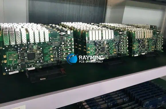
The technological revolution moves fast, and you cannot lag if you want to remain relevant and competitive. Such has proved the trend with printed circuit boards, especially in electronic design, manufacturing, and assembly. So are you an electronics PCB designer or enthusiast ready to understand more about the embedded PCB, new kid on the block? You cannot imagine a modern printed circuit board without the embedded PCB design coming to the fore.
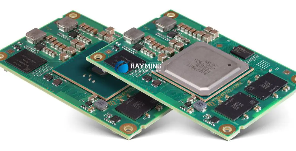
Embedded PCB

More recently, an increase in demand for wearable, electro-medical, and mobile devices has permeated every corner of the world. Consequently, demand for embedded PCBs increased, but a progressive size reduction of embedded PCBs. However, with the need for new attributes such as high-resolution display and wireless connectivity on devices, an increased pressure regarding increased component density on a reducing size poses exist and poses an unprecedented challenge that this PCB seeks to solve.  

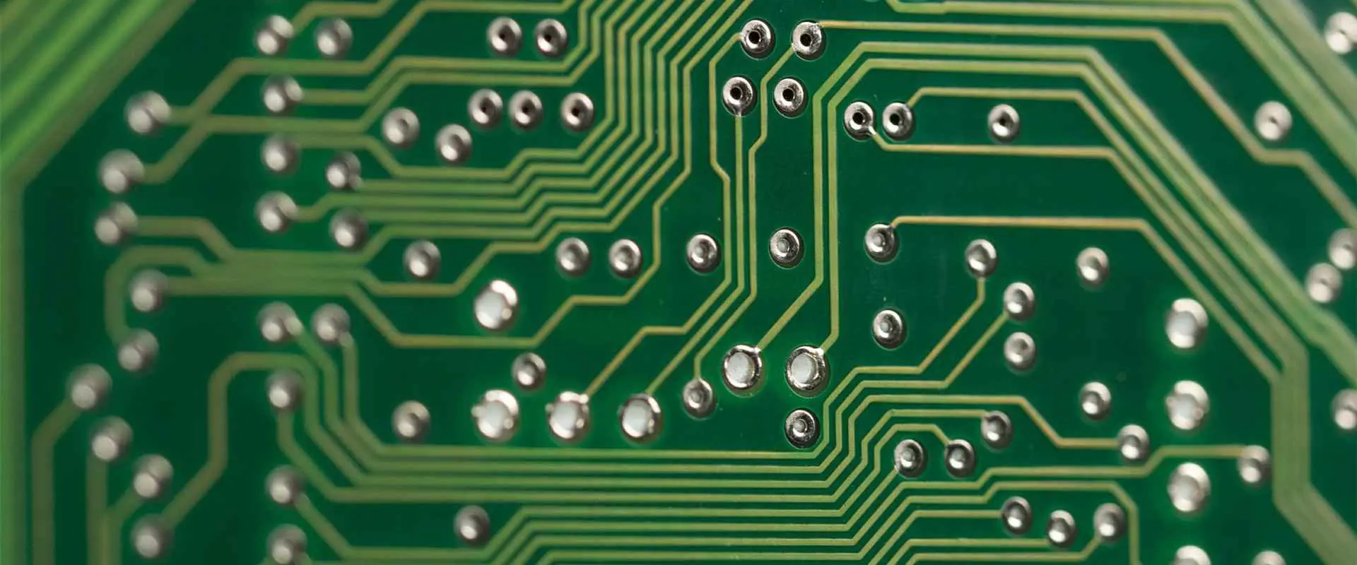
So what does an embedded PCB implies? An embedded PCB infers a printed circuit board containing embedded components to increase its efficiency and ensure high performance.  It always features an embedding technology that becomes instrumental in reducing transmission losses and shrinking the interconnection path among components. It plays a central role in the miniaturization of printed circuit boards, function integration, IP protection, and increased reliability.

The Assembly Process for Component Embedded Printed Circuit Board

One key feature of an embedded PCB design entails embedded components in PCB, with the embedding process encompassing the embedded technology.  The embedding technology includes mounting and involves two types: the Solder pad and the Thru-hole mounting methods.

  • Solder pad mounting method.  It involves the Bare dire and the Chip mounting processes. Firstly, the Bare method entails a wire mounting process or Flip-flop mounting. It would help if you chose which to go through with when trying to embed components on the PCB. Secondly, PCB in embedded system can also entail Chip mounting, where you can decide to adopt Wave soldering or Conductive resin.
  • Thru-hole mounting method. It also entails the Bare and Chip mounting processes, though the subsequent options differ from the Solder pad mounting methods. Here, the Bare mounting entails the Plated thru-hole or Conductive adhesive thru-hole options. The Chip mounting route also contains the same options: Plated thru-hole or Conductive adhesive thru-hole options.

Please note that the mounting method involving the embedded PCB with pad requires assembling the components on the formed electrodes besides developing the electrical connections. The application of the insulating resin can then get carried out to bury and fill the electrode and components, respectively.

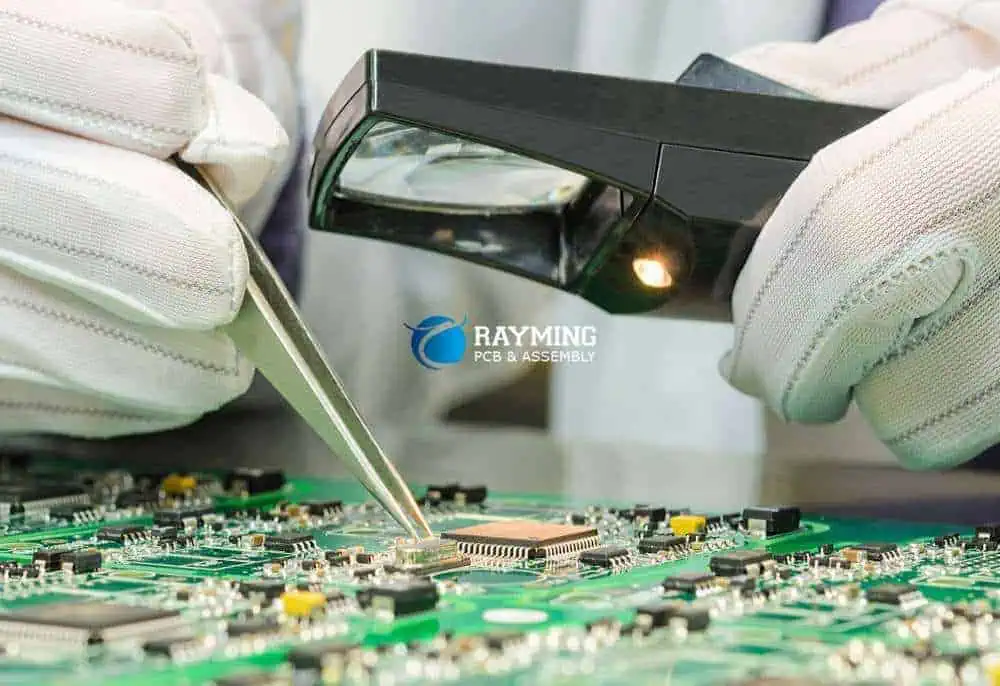
Assembly Procedure for Embedded Components in PCB

embedded components in pcb

Before looking at the assembly procedure, it becomes necessary to note the following down during the assembly process. Firstly, use the die bonding for bare die components and mold package for pad components. You can also use WLCSP, CCCC, Ultrasonic wave bonding, ESC, and conductive resin. However, for AD mounting, you can opt for conductive resin and wave solder.

To better understand the assembly process for component embedded PCB, it becomes crucial to take one mounting method in perspective and look at it in depth. So in this article, the embedded tech involving pads will become the mounting method on focus as an incredible example.

Assembly Procedure for Embedded Tech with Pads

  • Firstly, it becomes prudent to research technological and design procedures, especially when it comes to AD (buried into the PCB) tech feasibility and SMDs also embedded into the cavity of the PCB.
  • Trace design is the next integral step.
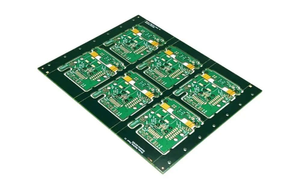
  • The embedded PCB’s manufacturing procedure comes as the subsequent step, and it involves a process. For a double layer PCB, it starts with the fabrication of the double-layer substrate before the coating of the solder paste. It then continues with the IC assembly and waves soldering before the insulation filling and mid-stack-up. Finally, the process ends with the top layer stack-up and hot pressing.
  • Assembly embedded components in the cavity
  • One key challenge with embedded that anyone will attest to involves the assembly of components in the cavity. You can face the possibility of failing to apply the old-fashioned solder paste printing tech of the planar pattern. In contrast, the smooth exhaustion of the gas in the cavity fails during the wave soldering. Consequently, it can all lead to high solder voidage. To avoid the occurrence of this scenario when using the vacuum wave soldering and solder printing techniques, the adoption of this workflow becomes crucialโ€”printing of solder paste, mounting, and vacuum wave soldering. After that, plugging, cleaning, and spray coating ensues before the process ends.  

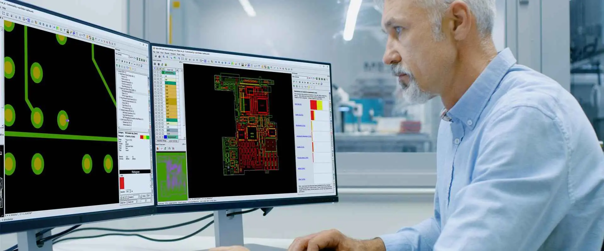
Printed Circuit Boards Design for Embedded Systems

The PCB design when it comes to embedded systems proves critical in an embedded PCB manufacturing process. Because of this, it becomes instrumental in knowing a few things about the PCB designs for such embedded systems.

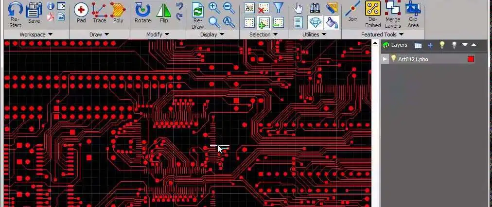
  • PCB size. Size often represents a major obstacle in the design of PCBs. Therefore, the printed circuit board size and layout need every party, from the designers to engineers, to agree on everything. However, one non-negotiable includes a specific minimum size limit that PCBs cannot go beyond. It cannot get too small because you have to ensure that the right component positioning happens and avoids overheating. The embedded system has passive components, and thus the need for an SMD tech becomes mandatory. It reduces the distance and footprint between components and thus results in a compact printed circuit board layout. The second aspect entails the optimization of the PCB routing. Additionally, if space permits, it becomes crucial to increase the layer number and trace placement.
  • Components placement.  Placement of the components often follows and reflects the PCB design rules. The rules involve an excellent alignment that allows a simple assembly and soldering process. Additionally, a proper separation has to get enforced between digital and analog devices. Finally, try and avoid placing some of the heavier components at or near the PCB edge, as the board can bend.
  • Thermal management. Heat tends to get produced on a printed circuit trace whenever a high-intensity current flows through it. Therefore, it becomes crucial to enhance thermal dissipation as you keep the size of the PCB small.  You can accomplish this through one of two techniques or a mix of both. It can involve increasing the thickness of the trace or develop the PCB regions to achieve heat dissipation. Because of this, ensure that you adhere to the suggested IPC2221A standard. It entails the copper planes having a thickness of 10 ounces, though the value can always increase. Additionally, the creation of hot spots should get eliminated by keeping the PCB maximum temperature under 170 อฆ C. You can always use a thermal imager to determine these hotspots. Another crucial way of enhancing heat dissipation also entails the insertion of thermal vias (holes drilled in the PCB substrate)
  • Embedded components. Most embedded systems feature small footprints and an elevated device density, all aimed at simplifying the assembly and design phases. Consequently, the resistors, inductors, and capacitors have to get embedded within the printed circuit board. It reduces the trace length, the number of solder points, besides the costs. What you achieve through this entails improved electrical performance besides circuit reliability. Capacitors, inductors, and resistors get placed on inner layers by etching in the PCB manufacturing process.  Subsequently, these components get incorporated during the PCB’s multi-layer lamination process. Inductors include those with magnetic cores, as the cores composed of ferromagnetic components get embedded within the substrate. Finally, the inductive windings get developed through photolithography.

Based on the components, diverse embedded tech variants can get deployed during the incorporation process. It results in new solution approaches and apps. However, in this, you will have to delve deeper into the different embedding technology variants, the process flows, design rules, selection criteria for the correct embedding variant, and the ET project’s workflow. Fortunately, you have already covered some of these processes by this point, and it should not become harder to comprehend.  

Step-Wise Process of Planning and Designing a Printed Circuit Board Assembly for Embedded Systems

  • Define the requirements. All designs need specified requirements, and you will have to set some before embarking on the assembling process. Define what the assembly requires and what will not become necessary in the process. Such entails the connection of parts and the size of the PCB.
  • Create a schematic. Once you have stipulated all the design requirements besides creating a concept to satisfy these needs, you will need to develop a comprehensive schematic. It should elaborate on all the components the PCB requires, the positions on the board, and the necessary connections between them. Of course, you also have to develop the bill for all components at this stage, and these involve material needs, current, and voltage requirements.
  • Automation software for electronic design. It helps when it comes to the incorporation of details once the schematic gets developed. The set of instruction here become instrumental in the assembly process.
  • Picking the method of fabrication
  • Here, the original requirements, budget, time required, and available resources will dictate what fabrication method to pick. However, all these bases get covered at RayMing PCB & Assembly Company to ensure your design specifications get produced.  
  • Testing. It encompasses the last step, and it involves the prescription of what tests to subject the PCB assembly in ensuring that all design requirements get fulfilled.  However, diverse testing techniques exist, and you will have to pick one that covers all the bases.

Conclusion

Embedded PCBs have become integral to all electronic devices because of the diverse specification needs users require. Therefore, if you want universal success and acceptance to your PCB design and one that outlives this period, an embedded PCB has to be your go-to PCB. Further, where better to get these services but on RayMing PCB & Assembly.  

PCB Pricing Guide: Factors Affecting Printed Circuit Board Costs (From Prototypes to Bulk Orders)

PCB Pricing

Introduction

In the ever-evolving world of electronics, Printed Circuit Boards (PCBs) serve as the backbone of countless devices, from smartphones to industrial machinery. Understanding PCB pricing is crucial for anyone involved in electronics development, from startup entrepreneurs to established manufacturers. The cost of PCBs can significantly impact product design decisions, prototyping processes, and ultimately, the final manufacturing cost of electronic devices.

This comprehensive guide delves into the multifaceted world of PCB pricing, exploring the various factors that influence costs from the initial prototype stage to large-scale production runs. By gaining insight into these factors, designers, engineers, and project managers can make informed decisions that balance quality, performance, and cost-effectiveness in their PCB projects.

1. Basics of PCB Pricing

1.1 What is a PCB?

A Printed Circuit Board (PCB) is a fundamental component in electronic devices, providing mechanical support and electrical connections for electronic components. PCBs consist of conductive pathways, tracks, or signal traces etched from copper sheets laminated onto a non-conductive substrate.

1.2 Why PCB Cost Matters

Understanding PCB pricing is crucial for several reasons:

  • For startups: Every dollar counts, and optimizing PCB costs can make or break a product’s viability.
  • For large companies: Even small savings per unit can translate to significant amounts when producing millions of boards.
  • For all businesses: Balancing cost with quality and performance is key to staying competitive in the electronics market.

1.3 Key Terms to Know

  • Prototype: Initial PCB version for testing and validation.
  • Batch Production: Manufacturing PCBs in small to medium quantities.
  • PCB Assembly (PCBA): The process of soldering components onto a bare PCB.
  • Minimum Order Quantity (MOQ): The smallest number of PCBs a manufacturer will produce in a single order.

2. Core Factors Affecting PCB Pricing

2.1 Material Costs

The choice of PCB material significantly impacts the overall cost. Common materials include:

Material TypeRelative CostTypical Applications
FR4LowGeneral purpose
RogersHighHigh-frequency, RF
AluminumMediumHigh power, LED
FlexibleHighWearables, flex circuits

The impact of material choice on PCB board price and printed circuit board price can be substantial. For instance, a high-frequency Rogers material can cost 5-10 times more than standard FR4.

2.2 Board Size and Layer Count

Board dimensions and the number of layers directly affect the circuit board price:

  • Larger boards require more material and processing time.
  • Multi-layer boards are more complex to manufacture than single or double-sided boards.

Cost differences based on layer count:

  • Single-layer: Base cost
  • Double-layer: ~1.5x to 2x single-layer cost
  • 4-layer: ~2.5x to 3x double-layer cost
  • 6-layer and above: Increases exponentially

2.3 Production Volume

The relationship between production volume and PCB cost per unit is inversely proportional:

  • Prototypes and small batches have higher per-unit costs due to setup fees and lower efficiency.
  • Bulk orders benefit from economies of scale, reducing per-unit costs significantly.

Minimum Order Quantity (MOQ) also plays a role in pricing. Manufacturers often offer better rates for orders meeting or exceeding their MOQ.

2.4 PCB Complexity

Several factors contribute to PCB complexity and, consequently, to the price:

  1. Via Types:
    • Through-hole: Lowest cost
    • Blind vias: Moderate increase in cost
    • Buried vias: Highest cost due to additional manufacturing steps
  2. Surface Finish:Finish TypeRelative CostDurabilityHASLLowModerateENIGHighHighImmersion SilverMediumGood
  3. Trace Width/Spacing and Tolerances: Tighter tolerances and finer traces increase manufacturing difficulty and cost.

2.5 Turnaround Time (Lead Time)

The speed of production significantly affects PCB pricing:

  • Standard production: Lowest cost, typically 5-10 business days
  • Quick-turn PCB orders: Higher cost, can be as fast as 24-48 hours
  • Express manufacturing: Premium pricing, same-day or next-day options available

Expedited orders can cost 50-100% more than standard lead times, depending on the urgency and complexity of the project.

Read more about:

3. Special Considerations in PCB Pricing

3.1 Custom PCB Price Factors

Custom PCB designs often incur additional costs due to:

  • Unique shapes or cutouts requiring special tooling
  • Specialty coatings or materials for specific environmental conditions
  • Non-Recurring Engineering (NRE) fees for design validation and tooling setup

These custom elements can increase the base PCB price by 20-50% or more, depending on the complexity.

3.2 Flexible PCB Price vs. Rigid PCB Pricing

Flexible PCBs generally cost more than rigid PCBs due to:

  • Specialized flexible or flex-rigid materials
  • More complex manufacturing processes
  • Higher scrap rates during production

Flexible PCBs can cost 30-50% more than equivalent rigid PCBs but offer benefits in space-constrained or dynamic applications.

3.3 PCB Assembly (Printed Circuit Assembly Price)

PCB Assembly (PCBA) adds significant cost to bare PCBs:

  • Component costs: Can range from a few cents to hundreds of dollars per component
  • Assembly method:
    • Surface Mount Technology (SMT): More efficient for high-volume production
    • Through-Hole: Labor-intensive, often more expensive for large volumes
  • Assembly labor costs vs. machine assembly:
    • Hand assembly: Higher cost, suitable for prototypes or small batches
    • Automated assembly: Lower per-unit cost, requires higher initial setup fees

PCBA can often double or triple the cost of a bare PCB, depending on the complexity and component costs.

3.4 Blank PCB Board Price and Zero PCB Price

For hobbyists and DIY markets, blank and “zero” PCBs offer low-cost options:

  • Blank PCB board price: Pre-made boards without specific circuit designs, often sold in standard sizes.
  • Zero PCB price: Some manufacturers offer free or extremely low-cost PCBs for small, simple designs to attract new customers.

These options typically range from 1โˆ’1โˆ’10 per board, making them accessible for beginners and prototyping.

4. Additional Costs in PCB Projects

4.1 PCB Manufacturing Machine Price

For companies considering in-house PCB production:

  • Small batch PCB machines:ย 5,000โˆ’5,000โˆ’50,000
  • Industrial-grade PCB manufacturing equipment:ย 100,000โˆ’100,000โˆ’1,000,000+

The decision to purchase PCB manufacturing equipment depends on production volume, required capabilities, and long-term cost analysis compared to outsourcing.

4.2 PCB Scrap Price and Recycling Value

Managing PCB waste affects overall manufacturing costs:

  • PCB scrap contains valuable metals (gold, copper) but also hazardous materials.
  • Proper recycling can recover some value but incurs processing costs.
  • Environmental regulations may require specific disposal methods, adding to overall project costs.

4.3 Amplifier PCB Board Price and LED PCB Board Price

Specialized PCBs often have unique pricing considerations:

  • Amplifier PCBs: May require higher-grade materials for signal integrity, increasing costs by 20-40%.
  • LED PCBs: Often use aluminum substrates for heat dissipation, potentially doubling the cost compared to standard FR4 boards.

5. Popular PCB Manufacturer Pricing Examples

5.1 PCBWay Price Structure

PCBWay offers competitive pricing for both prototypes and mass production:

  • Prototype pricing starts at $5 for 10 pieces of 100mm x 100mm boards.
  • Volume discounts available for larger orders.
  • Assembly services offered with varying pricing based on complexity and component costs.

Pros:

  • Competitive pricing for small to medium batches
  • Quick turn options available

Cons:

  • Higher shipping costs for some regions
  • Assembly costs can be higher than some competitors for large volumes

5.2 JLCPCB Pricing System

JLCPCB is known for its low-cost PCB manufacturing:

  • Offers extremely competitive prices, starting at $2 for 5 pieces of 100mm x 100mm boards.
  • Integrated PCB assembly service with a vast component library.
  • Significant discounts for larger orders.

Pros:

  • Very low prices for basic PCBs
  • Fast turnaround times
  • Extensive component library for assembly

Cons:

  • Limited options for advanced PCB technologies
  • Quality may vary for complex designs

6. How to Get the Best PCB Pricing

6.1 Tips for Lowering PCB Costs

  1. Design for manufacturability (DFM):
    • Use standard trace widths and clearances
    • Minimize the use of blind and buried vias
    • Choose common board sizes when possible
  2. Consolidate prototypes:
    • Combine multiple designs on a single panel to reduce setup costs
  3. Select appropriate specifications:
    • Don’t over-specify tolerances or materials beyond what’s necessary
    • Consider lead-free options only when required

6.2 Comparing Quotes from Multiple Manufacturers

  • Request quotes from at least 3-5 manufacturers
  • Compare not just price, but also quality, lead time, and customer service
  • Consider the total cost of ownership, including potential rework or quality issues

6.3 Understanding Hidden Fees

Be aware of additional costs that may not be immediately apparent:

  • Shipping fees, especially for international orders
  • Tooling charges for custom designs or non-standard features
  • Testing and inspection fees for high-reliability applications

7. Future Trends in PCB Pricing

7.1 Automated Manufacturing and Smart Factories

The increasing adoption of Industry 4.0 technologies in PCB manufacturing is likely to impact pricing:

  • Potential for lower costs due to increased efficiency and reduced labor
  • Higher initial investment in equipment may temporarily increase prices
  • More consistent quality could reduce overall project costs by minimizing rework

7.2 Impact of Material Shortages and Global Supply Chains

Recent global events have highlighted the volatility of supply chains:

  • Material shortages can lead to price fluctuations and longer lead times
  • Diversification of supply chains may increase resilience but potentially at a higher cost
  • Localized production might become more prevalent, affecting pricing structures

7.3 Innovations in PCB Recycling and Eco-friendly PCBs

As sustainability becomes a greater focus:

  • Development of more easily recyclable PCB materials could impact pricing
  • Potential for regulations on PCB disposal to affect overall project costs
  • Market demand for eco-friendly electronics may drive innovation in PCB materials and processes

Conclusion

Understanding the multifaceted nature of PCB pricing is crucial for anyone involved in electronics development and manufacturing. From material selection and board complexity to production volume and turnaround time, numerous factors influence the final cost of a PCB project.

Key takeaways for managing PCB costs effectively:

  1. Carefully consider design choices and their impact on manufacturability and cost.
  2. Balance quality requirements with budget constraints to avoid over-engineering.
  3. Plan strategically from prototyping to mass production, considering long-term costs and scalability.
  4. Stay informed about industry trends and technological advancements that may affect PCB pricing in the future.

By applying the insights from this guide, electronics professionals can make informed decisions that optimize PCB costs without compromising on quality or performance. As the electronics industry continues to evolve, staying adaptable and knowledgeable about PCB pricing factors will remain crucial for success in this dynamic field.

Applications and Types of PCB Glue

pcb adhesive

Gluing is an important process used in PCB fabrication and assembly for functions ranging from laminate bonding to strain relief. Selecting the proper adhesive or glue for the application helps ensure strong, reliable mechanical connections on printed circuit boards. This article provides an overview of the key uses of PCB glue as well as glue material properties and common glue types.

PCB Gluing Applications

Glue serves a variety of roles in PCB manufacturing:

  • Laminate bonding – Bonds layers of fibreglass in multilayer PCBs
  • Component attach – Glues components like resistors or capacitors to the PCB
  • Wire tacking – Temporary bonding of wires before soldering
  • Strain relief – Reinforces soldered connections against vibration/shock
  • Edge bonding – Bonds the edge of flex PCB layers
  • Masking – Protective coating over components or traces
  • Thermal interface – Glues heat sinks to devices

Choosing a PCB glue optimized for the specific application ensures the adhesive meets required performance criteria.

Glue Material Properties

PCB glues exhibit a range of material characteristics that determine their suitability for particular applications:

Bond Strength

  • Shear strength – Ability to withstand lateral force
  • Tensile strength – Withstand pulling/stretching force
  • Impact resistance – Absorb sudden impacts without breaking bond

Cure Process

  • Room temperature cure – Cures through oxidation at room temperature
  • UV light cure – Cures quickly under UV exposure
  • Heat cure – Cures at elevated temperature

Thermal Properties

  • Operating temperature range
  • Glass transition temperature
  • Coefficient of thermal expansion
  • Thermal conductivity

Electrical Properties

  • Dielectric strength – Resists electrical breakdown under voltage
  • Volume resistivity – Resists conduction of electricity
  • Dielectric constant – Ability to store charge in an electric field

Outgassing – Release of gaseous vapors during cure. Important for aerospace applications.

Reworkability – Ability to detach/rework bonds for repair needs

PCB Glue Types

Here are some of the common adhesive types used in PCB fabrication and assembly.

Epoxy

Epoxies are the primary adhesives used to laminate multilayer PCBs. They cure through a chemical reaction between epoxide resin and a curative hardener. Key properties:

  • Exceptional bond strength and temperature resistance
  • Low outgassing and high dielectric strength
  • Long working life for easier application

Epoxies come in a variety of formulations tuned for flexibility, thermal shock resistance, etc.

Acrylic

Acrylic adhesives cure through exposure to ultraviolet radiation. They are often used for component attachment on the PCB surface. Benefits include:

  • Cure rapidly under UV light
  • Room temperature storage before curing
  • Good dielectric and thermal properties

Cyanoacrylate

Cyanoacrylates, or super glues, are fast-curing adhesives used for wire tacking and temporary bonding during assembly. Properties:

  • Extremely rapid room temperature cure
  • Low viscosity for wicking into joints
  • Ability to cure with minimal moisture
  • High shear and impact strength

CA glues provide quick, strong, temporary bonds.

Silicone

Silicone adhesives cure at room temperature through reaction with moisture in the air. Applications include:

  • Flexible strain relief for cables or connectors
  • Thermal insulation or heat transfer
  • Edge bonding of conformal electronics
  • Masking sensitive components on the PCB

Silicones provide good flexibility, dielectric strength, and thermal conductivity.

Urethane

Urethane adhesives cure with moisture at room temperature. They are used when flexibility is needed:

  • Bonding rigid and flexible circuits
  • Absorbing vibration, shock, and stress
  • Edge sealing flexible PCBs
  • Adhering metal component tabs

Urethanes have good impact and chemical resistance.

Selecting a PCB Glue

Factors to consider when selecting an appropriate PCB glue include:

Strength – Tensile, shear, impact needs

Flexibility – Rigid or flexible cured bond

Temperature Range – Max operating temperature

Cure Process – Heat, UV, room temperature

Dielectric Properties – Dielectric strength, resistance

Conductivity – Thermal and/or electrical

Chemical Resistance – Solvent, moisture, etc.

Outgassing – For vacuum or aerospace environments

Reworkability – May need temporary or removable bond

Discuss application requirements with glue suppliers to identify the best adhesive product fit.

PCB Glue Application Methods

Common methods for applying PCB glues include:

  • Dispensing – Depositing precise dots or lines through needles
  • Screen Printing – Using a stencil to print adhesive
  • Roller Coating – Rolling a thin adhesive film onto bonding surfaces
  • Spraying – Aerosol spraying in open or controlled environments
  • Brushing – Manual application with brushes

Automated precision dispensing or printing ensures consistency and minimizes waste.

Quality Control

To achieve reliable, consistent bonds, PCB gluing processes require controls including:

  • Testing bond strength of each batch with destructive tests
  • Monitoring adhesive viscosity, especially for dispensed dots
  • Keeping cold storage within specified temperature range
  • Avoiding exposure to moisture before application
  • Using glue within recommended shelf life
  • Curing bonds fully with thermal ramps or UV cycles
  • Inspecting visually for complete coverage without voids
  • Tracking process parameters like time, temperature, pressure

Like soldering, gluing is a manufacturing process requiring close monitoring and control.

Conclusion

Gluing is a critical process used across PCB fabrication, component attachment, wire bonding, and protecting assemblies. The wide range of PCB glues available allows selecting formulations optimized for specific applications and performance requirements. Keeping gluing processes under tight quality control ensures boards with strong, reliable adhesive bonds.

PCB Glue FAQ

Q: What are some key considerations when selecting a PCB laminate bonding glue?

A: Matching Tg, thermal conductivity, dielectric properties, temperature resistance, and flexibility needs of the board. Also consider resin flow viscosity and working life.

Q: How is cured glue reworked on a PCB?

A: Removing cured glue mechanically can damage boards. Rework generally involves heating to soften the glue for removal. Laser ablation can also detach glue.

Q: What processes can help improve adhesion of PCB glues?

A: Surface roughening through chemical or mechanical abrasion gives more surface area. Plasma surface activation also improves bond strength. Match coefficients of thermal expansion.

Q: What safety precautions are important when working with PCB glues?

A: Adhesive fumes require good ventilation. Cured blobs can be sharp. Cured cyanoacrylates generate heat. Follow all material safety datasheet (MSDS) guidelines.

Q: How is PCB glue viscosity monitored and controlled?

A: Viscometers measure viscosity. Adhesives are kept in cold storage to inhibit curing and maintain viscosity. Dispense process parameters may need adjustment to account for viscosity shifts over adhesive lifetime.

Uses of PCB glue on electronics

The electronic industry largely depends on printed circuit boards as the main components. The PCB utilizes adhesive materials in encapsulating components, conformal coating, wire tacking, and bonding surface-mount components.

A distinctive PCB is a multi-overlay built-up plastic board with a defensive plastic covering. At first, manufacturers used hardware to cover boards. They interconnected multi-facet boards ‘thru-hole innovation using drilled holes. Component and board scaling down prompted ‘surface-mount innovation’ during the 1980s. With surface-mount innovation, segment contacts are bound straightforwardly to pad sections on the outside of the board. It made it conceivable to dispose of through-board connections and drilled openings.

YouTube video

There is significant utilization for PCB glue, basically natural, are as per the following:

Bonding activities

  1. Conformal coatings

While it is not rigorously the aftereffect of a glue holding measure,  you can use similar substance kinds of gum. For example, silicones, acrylics, polyurethanes, and epoxy glue for PCB. The point is to deliver a covering that certainly sticks to and covers all the board and its parts. A conformal covering is commonly used to shield the board from natural factors, for example,

  • Short circuits.
  • Dampness and mold changes in help temperature (ordinarily from – 40ยบC to +200ยบC)
  • Corrosion

Conformally covered PCBs are shielded from natural harm and mechanical and electrical obstruction.

  •  Encapsulation and potting

It is a strategy for covering little surfaces or spaces with a material that will shield parts from physical and ecological harm. Encapsulation parts likewise give extra protection ability.

Potting compounds typically display excellent synthetic properties and high grip to plastics and metals, these being the materials of development of the holders and the parts.

Regular saps utilized for encapsulating are acrylics, silicones, polyurethanes, and epoxies, the last as a rule being UV-relieving definitions.

Similarly, there are different techniques for exemplifying electronic segments, to be specific projecting and trim. Projecting utilizes similar glue as preparing, albeit the compartment is generally eliminated after the pitch has been relieved.

Dissimilar to the potting cycle where the holder turns into a fundamental piece of the segment. For the most part, Embellishment includes the infusion of pre-dissolved thermoplastic pitches into a form containing the electronic components or hardware.

pcb component glue
  • Wire-tacking glues

Connection using wires is normal on PCBs. The utilization of wires permits substitution as well as an increase of printed wiring on the PCB. A portion of the explanations behind this is as per the following:

  • To fix board harm or defeat the impacts of ill-advised assembling.
  • To redesign or change a PCB.
  • To conquer a plan imperfection found during board testing.

Typically, a protected wire is stripped and bound at each finish to cushions and part drives, at that point fortified or marked to the board substrate. The holding keeps the wire from moving around and goes about as an underlying glue in conditions where vibration could happen.

The glue that one can choose for wire attaching incorporates light-reparable acrylics, epoxies, and cyanoacrylates. Practically speaking, cyanoacrylates are generally utilized, regularly related to a suitable activator to speed the fixed time to around half a minute.

  • Surface-mount devices (chip holding)

Surface-mount devices (SMDs) are set on little dots or spots of uncured glue and afterward relieved set up by warming or openness to UV radiation. It gets the SMDs solidly set up during resulting measure tasks like leaded-gadget addition or cleaning until they can be fastened to the board’s patch pads. Surface-mount glue can serve two capacities: they go about as a handling help (for example, holding a section briefly until it tends to be for all time appended by patching). They can likewise give pressure alleviation to bind connection during administration to forestall untimely disappointment of the electrical bonds. Subsequent to soldering, the now repetitive glue should not any effect on the hardware at all.

To meet the necessities for effectively holding SMDs, the accompanying properties are expected of the glue:

  • Good electrical properties after curing
  • High strength and good flexibility
  • Non-slumping during the heated cure cycle
  • Rapid curing
  • High wet strength
  • Non-stringing
  • Suitability for high-speed dispensing of very small dots of consistent profile and size
  • Long shelf life

Contingent upon the specific capacity of the surface-mount glue, it tends to be electrically conductive, electrically non-conductive, and thermally conductive. Three compound kinds of glue are generally utilized for surface-mount segment holding: acrylics, epoxy glue, and urethane acrylates. These glue variants, along with different sorts utilized in hardware applications, are talked about in more prominent detail beneath.

Preferably, surface-mount glues should be of the single component type. It maintains a strategic distance from pot-life issues, air entanglement, and changes in thickness ordinarily connected with double or multi-part frameworks. Usually, the glues will fix inside two minutes at raised temperatures alright for PCBs and related parts.

Types of glue for circuit boards

PCB Glue

We need to consider three diverse handling stages while choosing circuit board adhesive applications. They include the solid-material or cured phase, the curing (transitional) phase, and the liquid-resin or uncured phase. The presentation of the solid-material adhesive is eventually the most significant since it enhances quality.

The technique for applying the PCB component glue is critical, specifically given the need to guarantee that the right sum is applied in the right spot. Significant techniques for applying glues in hardware applications are syringe application, pin transfer, and screen printing. Syringe application is presumably the most famous strategy, ordinarily via electro-pneumatically controlled syringes for moderate creation of a wide range of kinds of PCB.

The different kinds of glue for circuit boards include:

  1. Ultraviolet curing glues

Light-curing encapsulants, coatings, and adhesives are being utilized in the hardware producing industry, expanding recurrence since they meet the necessities for materials and preparing inside this industry. Those elements incorporate ecological protection policies (environmentally damaging solvents and added substances are not needed), fabricating yield improvement, and item cost. Light-curing glues are easy to utilize and are immediately relieved without the requirement for raised temperature relieving.

The glues are regularly acrylic-based details and contain photograph initiators that actuated by bright radiation, structure-free revolutionaries to start the polymer-shaping (relieving) measure. Bright light should have the option to infiltrate into the uncured sap, a downside of light-curing glues. Stores of pitch that are dimly shaded, blocked off, or thick are hard to fix.

Scaling down electronic hardware may bring about issues of heat arise, which can cause untimely malfunction of electronic parts if their most fantastic working temperature is surpassed. Thermally conductive glue can give a heat-directing way, securing semiconductors, diodes, or other force gadgets to appropriate heat sinks to guarantee such a temperature does not happen.

Non-metallic (insulating) or metallic (electrically conductive) powders are mixed into the glue plan to make high-thickness glues, which are exceptionally thermally conductive. The most well-known hot glue PCB is formed with acrylics, silicone, and epoxy.

  • Electrically conductive PCB adhesive

By their inclination, most glues, both natural and inorganic, are not electrically conductive. It applies to the principle types utilized in electronic applications. They include cyanoacrylates, urethane acrylates, silicones, cyanoacrylates, acrylics, and epoxy glue for PCB. Notwithstanding, in numerous applications, including coordinated circuits and surface-mount gadgets, electrically conductive glues are required.

There are two sorts of electrically conductive glues, which are anisotropic and isotropic. Anisotropic glues are good conductors in all directions. However, an isotropic glue conducts in the upward (z-pivot) heading just and is in this way uni-directional. The isotropic glues loan themselves to almost negligible difference interconnection. It ought to be noticed that valuable as conductive glues are, they cannot be essentially ‘dropped in’ as patch choices. They are bad with tin or aluminum, nor where there are enormous holes or where they are probably going to be presented to wet conditions in help.

The typical method of changing non-conductive glues over to electrically conductive materials is to add reasonable filler to the base material. Generally, the last is an epoxy pitch. Commonplace fillers used to give electrical conductivity are carbon, nickel, and silver. Silver is the most broadly utilized. The conductive glues themselves are either in a fluid or pre-structure.

  • Other glue types

The glues referenced above are the significant sorts utilized in ordinary gadgets fabricating strategies. There are others, nonetheless, which are still generally utilized:

  • Polyimides: These are high-temperature saps (enduring up to 300ยบC or somewhere in the vicinity) utilized in high technology hardware applications (ordinarily aviation) for wire coatings and adaptable circuits. They usually are utilized as polyamic corrosive forerunners and require troublesome and delayed restoring cycles before shaping the average adaptable, heat-safe polyamide material.
  • Silicone resins: More a sealant than a primary glue, silicone sap is utilized as an encapsulant just as for conformal covering. Silicone pitches have excellent low and high warmth resilience (regularly – 60ยบC to +200ยบC) yet can mess up optional activities on account of the arrival of low-sub-atomic weight silicone compounds, which sully surfaces over a wide region.
  • Cyanoacrylates: These have effectively been referenced for their utilization in wire-attaching applications. Cyanoacrylates are single-part glues, which fix quickly when presented to dampness noticeable all around. The utilization of these glues with an activator speeds up the relieving interaction significantly more.

There are significantly more glues, which have discovered use in hardware applications, and without a doubt, more will follow. Nonetheless, the sorts referenced above are grounded and generally utilized and structure a fundamental piece of the gadgets fabricating industry.

Conclusions

The gadgets market involves a wide range of enterprises, including media communications, customer, PC, and car areas, utilizing the PCB as the fundamental structure block for their items. Several years ago, the measure of glues utilized in creating PCBs and other electronic parts was insignificant. Presently the shortfall of glues from gadgets producing is incomprehensible. Natural, wellbeing, cost, and assembling speed are driving variables for the proceeding and always growing utilization of glues in the business.

The days when soldering was the elite joining technique in PCBA have a distant memory. The point currently is to zero in on the utilization of glues as patch choices. There is still some best approach, as the glue should assume control over the mechanical properties of the bind and be electrically and thermally conductive to a serious level.

What is PCB DFM (Design for Manufacturing)?

PCB DFM

The term DFM (Design for Manufacturing) refers to the process of designing a product with the specific goal of simplifying its manufacturing, resulting in a better product at a reduced cost. Ideally, DFM should be implemented during the early stages of a project and should involve the entire product development team, not just the hardware designers. As the project advances through the various phases of the product life cycle, any changes to the original design become increasingly costly and complex to implement, sometimes to the point of being impractical.

On the other hand, applying DFM principles during the initial stages of PCB (Printed Circuit Board) development enables potential modifications to be made quickly, at minimal cost, while preserving the product’s original performance. Technology plays a pivotal role in many aspects of modern life. From smartphones and smartwatches to household appliances and connected vehicles, nearly every device relies on smart technology and connectivity. These applications demand increasingly complex printed circuits, which must be produced at the lowest possible cost, in the shortest time frame, and with the highest level of quality. DFM helps meet these challenges by optimizing the design process for efficient and cost-effective manufacturing.

Learn more about:

What is Design for Manufacturability for PCBs?

Design for Manufacturability (DFM) in the context of PCBs refers to the practice of designing circuit boards with manufacturing processes and limitations in mind. The goal is to create designs that can be easily, reliably, and cost-effectively manufactured at scale.

DFM considerations encompass various aspects of PCB design, including:

  1. Component placement
  2. Trace routing
  3. Layer stackup
  4. Material selection
  5. Drill hole specifications
  6. Solder mask and silkscreen applications

By incorporating DFM principles from the outset of your design process, you can significantly reduce the likelihood of manufacturing issues, minimize production costs, and improve the overall quality of your PCBs.

YouTube video

What Happens When You Ignore Your Manufacturer’s Capabilities

Ignoring your manufacturer’s capabilities can lead to a host of problems:

  1. Increased production costs due to necessary design revisions
  2. Manufacturing delays
  3. Quality issues in the final product
  4. Reduced yield rates
  5. Potential functionality problems in the finished PCBs

By adhering to DFM guidelines and working closely with your manufacturer, you can avoid these pitfalls and ensure a smooth transition from design to production.

What is DFM Analysis?

DFM analysis is a systematic review of a PCB design to identify potential manufacturing issues before production begins. This process typically involves software tools that check the design against a set of predefined rules based on manufacturing capabilities and industry standards.

Key aspects of DFM analysis include:

  1. Checking for violations of minimum spacing requirements
  2. Verifying drill hole sizes and locations
  3. Ensuring adequate copper thickness for current-carrying capacity
  4. Confirming that components can be placed and soldered correctly
  5. Verifying that the design meets the manufacturer’s specific capabilities

DFM analysis helps designers catch and correct potential issues early in the design process, saving time and money in the long run.

Files Required for Fabrication

gerber D-code
gerber D-code

To ensure successful PCB fabrication, manufacturers typically require the following files:

  1. Gerber files: These contain information about the copper layers, solder mask, and silkscreen.
  2. Drill files: These specify the location, size, and type of all holes in the PCB.
  3. Bill of Materials (BOM): This lists all components used in the design.
  4. Assembly drawings: These show the placement and orientation of components on the board.
  5. Fabrication drawing: This includes board dimensions, layer stackup, and other special requirements.
  6. ODB++ or IPC-2581 files: These newer formats can replace multiple separate files with a single, comprehensive data package.

Providing complete and accurate files is crucial for avoiding misunderstandings and ensuring that the manufactured PCB matches your design intent.

DFM Checks for Drill Holes

Proper drill hole design is critical for PCB functionality and manufacturability. Two key aspects to consider are aspect ratio and drill-to-copper spacing.

Aspect Ratio

Aspect ratio in PCB drilling refers to the ratio of the hole depth to its diameter. A high aspect ratio (deep, narrow holes) can be challenging to drill accurately and plate properly.

  • Most manufacturers prefer aspect ratios of 10:1 or less
  • Higher aspect ratios may require special processes and increase costs
  • Consider using stacked or staggered vias for high-density designs

Drill-to-Copper

Drill-to-copper spacing refers to the distance between a drilled hole and nearby copper features. Insufficient spacing can lead to:

  • Breakouts (where the drill bit intersects with nearby copper)
  • Electrical shorts
  • Reduced structural integrity

Typical minimum drill-to-copper distances range from 5 to 10 mils, depending on the manufacturer’s capabilities and the specific design requirements.

DFM Signal Checks

Signal integrity is crucial for PCB performance. Two primary considerations in DFM signal checks are conductor width and spacing.

Conductor Width

Conductor width affects both the current-carrying capacity and the impedance of traces. DFM checks ensure that:

  • Trace widths are within manufacturable limits (typically 3-5 mils minimum)
  • Traces are wide enough to handle expected current loads
  • Trace widths are consistent for controlled impedance requirements

Spacing

Proper spacing between conductive elements is essential to prevent shorts and maintain signal integrity. DFM checks verify:

  • Minimum spacing between traces (typically 3-5 mils)
  • Adequate clearance between traces and board edges
  • Proper spacing around vias and pads

Maintaining appropriate spacing helps ensure reliable PCB performance and reduces the risk of manufacturing defects.

Solder Mask Checks

Solder mask is a crucial element in PCB manufacturing, providing insulation and protection to the copper layers. Several aspects of solder mask design require careful consideration in DFM checks.

Solder Mask Clearance

Solder mask clearance refers to the space between the solder mask and exposed copper areas (like pads and vias). Proper clearance ensures:

  • Adequate space for soldering components
  • Prevention of solder bridges between adjacent pads
  • Reduced risk of solder mask dam failure

Typical minimum solder mask clearances range from 2 to 4 mils, depending on the manufacturer’s capabilities.

Solder Mask Opening

Solder mask openings are areas where the copper is intentionally exposed for soldering or testing. DFM checks ensure that:

  • Openings are large enough for reliable soldering
  • Openings are properly aligned with underlying copper features
  • There are no unintended openings that could lead to shorts or corrosion

Solder Mask Expansion

Solder mask expansion refers to how much the solder mask extends beyond the edge of a pad or via. Proper expansion helps to:

  • Prevent solder bridges between adjacent pads
  • Ensure adequate coverage of copper traces
  • Improve the overall appearance of the board

Typical solder mask expansion values range from 1 to 3 mils.

Solder Mask Registration

Solder mask registration refers to the alignment of the solder mask layer with the underlying copper features. Poor registration can lead to:

  • Exposed copper traces, increasing the risk of shorts
  • Covered pads, making soldering difficult or impossible
  • Aesthetic issues that may affect the perceived quality of the board

DFM checks verify that the solder mask is properly aligned within the manufacturer’s tolerances.

Solder Mask Relief or Solder Mask Web

Solder mask relief (also known as solder mask web) refers to the minimum width of solder mask between adjacent pads or other openings. Adequate relief is crucial for:

  • Preventing solder bridges between adjacent pads
  • Ensuring the structural integrity of the solder mask layer
  • Facilitating proper component placement and soldering

Typical minimum solder mask web widths range from 3 to 5 mils.

Silkscreen Checks

Silkscreen provides important information on the PCB, such as component designators, polarity indicators, and warnings. DFM checks for silkscreen ensure that this information is legible and doesn’t interfere with other PCB features.

Silkscreen to Mask Spacing

Proper spacing between silkscreen and solder mask openings is crucial for:

  • Ensuring silkscreen legibility
  • Preventing silkscreen from interfering with soldering processes
  • Maintaining a professional appearance

Typical minimum silkscreen to mask spacing is around 5 mils.

Silkscreen to Copper Spacing

Adequate spacing between silkscreen and exposed copper areas helps to:

  • Prevent silkscreen from interfering with electrical connections
  • Ensure proper adhesion of the silkscreen ink
  • Maintain the integrity of both the silkscreen and copper features

A minimum spacing of 5 mils is often recommended.

Silkscreen to Hole Spacing and Route Spacing

Proper spacing between silkscreen and holes or routed areas is important for:

  • Preventing silkscreen from falling into holes or routed areas
  • Ensuring the legibility of silkscreen near board edges
  • Maintaining a clean, professional appearance

Typical minimum spacing is around 10 mils for holes and 20 mils for routed edges.

Why Should You Perform DFM Checks?

Performing DFM checks offers numerous benefits:

  1. Reduced manufacturing costs by catching issues early
  2. Improved product quality and reliability
  3. Faster time-to-market by minimizing design revisions
  4. Better communication with manufacturers
  5. Increased yield rates in production
  6. Enhanced overall design efficiency

By integrating DFM checks into your design process, you can create more manufacturable PCBs and streamline the transition from design to production.

5 Common DFM Issues to Avoid in Your PCB Design

1. Floating Copper/Solder Mask Slivers Create Antennas

Floating copper areas or small slivers of solder mask can act as unintended antennas, potentially causing electromagnetic interference (EMI) issues. To avoid this:

  • Remove isolated copper areas not connected to any nets
  • Ensure proper copper pour connections
  • Verify minimum solder mask sliver widths (typically 3-5 mils)

2. Starved Thermals Cause Soldering Issues

Starved thermals occur when there’s insufficient separation between a pad and the surrounding copper pour. This can lead to:

  • Difficulty in soldering components
  • Cold solder joints
  • Increased risk of component damage during soldering

Ensure proper thermal relief design with adequate spoke width and air gap.

3. Absence of a Clearance Pad on the Pin Causes Short

When a through-hole component pin doesn’t have a clearance pad on non-component layers, it can cause shorts with copper features on those layers. To prevent this:

  • Use proper pad stacks for through-hole components
  • Ensure clearance pads on all layers for through-hole pins
  • Verify that clearance pads are large enough to account for drilling tolerances

4. Insufficient Annular Ring Results in an Open Circuit

annular ring
annular ring

An annular ring is the copper surrounding a drilled hole. Insufficient annular ring can lead to:

  • Open circuits if the hole misses the pad entirely
  • Weak connections prone to failure
  • Difficulties in plating the hole

Ensure that annular rings meet the manufacturer’s minimum requirements, typically 5-7 mils for outer layers and 3-5 mils for inner layers.

5. Copper Too Close to the Board Edge Causes Shorts in Adjacent Layers

Copper features too close to the board edge can cause problems during depanelization and increase the risk of shorts between layers. To avoid this:

  • Maintain a copper-free zone near board edges (typically 10-20 mils)
  • Use proper board edge clearance for components and traces
  • Consider using edge plating techniques for designs requiring copper near edges

Checks for Controlling DFM Issues

1. Avoiding DFM Issues in Drilled Holes

To minimize DFM issues related to drilled holes:

  • Use standard drill sizes whenever possible
  • Maintain proper aspect ratios (typically 10:1 or less)
  • Ensure adequate spacing between holes and other features
  • Consider using buried or blind vias for high-density designs

2. Designing Annular Rings Without Any Breakouts

To create robust annular rings:

  • Use larger pad sizes for critical connections
  • Account for drill tolerances in pad size calculations
  • Consider teardrop pads for improved reliability
  • Verify annular ring sizes meet manufacturer specifications

3. Efficient Trace Routing to Limit DFM Issues

Proper trace routing is crucial for manufacturability:

  • Maintain consistent trace widths for each net
  • Use 45-degree angles instead of 90-degree turns
  • Avoid running traces between pads of fine-pitch components
  • Consider using differential pair routing for high-speed signals

4. DFM Checks for Solder Mask Clearance

Proper solder mask clearance is essential for reliable soldering:

  • Ensure adequate clearance around pads and vias
  • Verify solder mask dam widths meet manufacturer requirements
  • Use consistent solder mask expansion values across the board

Design Tips for Solder Mask Clearance

  • Use larger clearances for fine-pitch components
  • Consider selective solder mask removal for sensitive areas
  • Verify solder mask clearances with your manufacturer’s capabilities

5. DFM Checks for Silkscreen

Proper silkscreen design ensures clear and durable board markings:

  • Verify minimum text sizes for legibility (typically 50 mils)
  • Ensure adequate spacing between silkscreen and other features
  • Use vector-based fonts for improved quality

Silkscreen Considerations During Circuit Designs

  • Place component designators in consistent locations
  • Avoid placing silkscreen on pads or vias
  • Consider using both top and bottom silkscreen for dense designs

By implementing these DFM checks and design considerations, you can significantly improve the manufacturability of your PCB designs, reduce costs, and ensure higher quality end products.

How to Choose SMT Manufacturing Factory for Electronic Production ?

smt manufacturing

Selecting the right surface mount technology (SMT) manufacturing partner is crucial for successfully producing electronic products. This article provides guidance on criteria to evaluate when choosing an electronics contract manufacturer with SMT capabilities for your assembly needs.

Overview of SMT Manufacturing

SMT is the predominant method of assembling printed circuit boards (PCBs) in electronics due to its speed, precision, and automation advantages over through hole assembly. In SMT:

  • Components are mounted directly on surface of PCB
  • High speed automated pick and place machines populate components
  • Solder paste applied to pads through stencil
  • Reflow oven melts solder to attach components

High mix SMT lines can place tens of thousands of components per hour on PCBs with precision less than 0.1mm.

Key advantages of SMT:

  • Higher component density allowing miniaturization
  • Lead-free processing
  • Lower assembly costs at high volumes
  • Improved reliability from process control
  • Flexible component selection

Electronics OEMs rely on contract manufacturers for their expertise in SMT production.

Key SMT Manufacturing Capabilities

SMT soldering Process

When evaluating contract manufacturers, consider their capabilities in these key SMT areas:

Equipment Technology

  • High speed, high accuracy pick and place machines
  • Advanced solder paste printing and dispensing
  • Reflow ovens supporting lead-free profiles
  • In-line inspection equipment – SPI, AOI, X-ray
  • Automated test handlers
  • Material handling automation – feeders, trolleys
  • ESD control equipment

Newer equipment supports tighter tolerances for miniaturized PCBs. Look for regular tech refresh investments.

Manufacturing Processes

  • Solder paste printing and inspection
  • Pick and place program optimization
  • Automated optical inspection
  • X-ray inspection for BGAs/QFNs
  • AXI for accepting and reworking defects
  • Testing and burn-in
  • Conformal coating
  • Box build and product integration

Quality processes like SPI/AOI and testing should be standard practice.

Materials and Components

  • Procurement systems with qualified suppliers
  • Traceability systems for lot control and recalls
  • Handling of moisture sensitive components
  • Access to hard-to-find and long leadtime parts
  • Management of component reels/tapes
  • Shelf life control for solder paste

Look for disciplined material control and risk mitigation programs.

Certifications

  • ISO 9001/13485 Quality Management
  • IATF 16949 Automotive Quality
  • AS9100 Aerospace Quality
  • ISO 14001 Environmental
  • OHSAS 18001 Health and Safety

Certifications validate disciplined management systems are in place. Make sure certs are current.

Assessing Technical Expertise

Look for expertise in:

  • Design for Manufacturing (DFM) – Optimizing board designs for processing
  • Process engineering – Programming machines, optimizing lines, troubleshooting
  • New product introduction (NPI) – Managing ramp up of new assemblies
  • Product and quality engineering – Applying robust quality practices
  • Test engineering – Developing test coverage for functionality and reliability
  • Process improvement – Applying LEAN, Six Sigma, SPC
  • ESD control – Following standards for handling ESD-sensitive devices

Cross-trained technical teams indicate an environment focused on quality.

Evaluating Operational Capabilities

Consider range of operational capabilities:

  • Volume Scalability – Ability to scale from prototypes to high volume production
  • Mix Flexibility – Managing high mix, low to medium volume production
  • Changeovers – Quickly switching between product variants
  • Multi-line Management – Coordinating production across lines and sites
  • Shortened Lead Times – Responding rapidly to priority orders
  • Inventory & Materials Management – Avoiding part shortages that cause delays

Look for expertise in necessary operational models like high mix/low volume and short lead time.

Assessing Supply Chain Maturity

Mature supply chain practices minimize delays:

  • Supplier Management – Qualification, audits, incoming inspection
  • Inventory Control – Tracking shelf life and availability
  • Logistics Partners – Negotiated rates, responsiveness
  • Sales & Operation Planning – Aligning supply plan with demand
  • Inventory Risk Management – Dual/alternate sources for key items
  • Lead Time Reduction – Supplier agreements and procurement optimization

Choose a partner who helps de-risk the electronics component supply chain.

Evaluating Continuous Improvement Culture

  • Use of PDCA cycles and structured problem solving
  • Applying LEAN and Six Sigma principles
  • Fostering feedback culture between teams
  • Technology acceleration programs (e.g. AI, IoT)
  • Employee training and advancement programs
  • Established EHS and sustainability programs

Look for obsession with continuous improvement at all levels and functions.

Assessing Engineering Collaboration Capability

through-hole assembly process
  • Design for Manufacturing (DFM) expertise
  • New Product Introduction (NPI) program structure
  • Joint process capability assessment
  • Dedicated engineering contacts
  • Use of digital tools for collaboration
  • Data transparency and analytics
  • Managing product lifecycle and change management

Choose a partner who integrates with your engineering processes.

Considering Global Logistics Support

  • Tax and duty optimization knowledge
  • Consolidated ocean and air freight
  • Well negotiated rates with carriers
  • Automated customs forms and compliance
  • Layer packing and crating capability
  • Global order visibility and documentation
  • Regional warehouse hubs and fulfillment

Global supply chain support provides flexibility in your fulfilment model.

Prioritizing Corporate Responsibility

  • Employee health, safety and workplace practices
  • Environmental sustainability initiatives
  • Established ethics policies and controls
  • Data security and IP protection regime
  • Product safety and regulatory compliance
  • Contributing back to communities

Shared commitment to social responsibility reduces supply chain risks.

Verifying Financial Stability

  • Multi-year track record of revenue and growth
  • Established customer base across industries
  • Disciplined management of debt and cash flow
  • Investment in facilities and technologies
  • Global footprint with regional options
  • Publicly traded or PE/VC backed companies

Choose an SMT partner on solid long-term financial footing.

Conclusion

Selecting the right SMT manufacturing partner requires thorough vetting across technical, operational, supply chain, quality, and financial considerations. Alignment between engineering teams is also key. Taking the time upfront to perform due diligence reduces program risks and sets the foundation for a lasting partnership driving electronic product success.

How to Choose SMT Manufacturing Partner – FAQ

Q: What volume production capabilities should be expected from an SMT CM?

A: A strong SMT partner should be able to scale efficiently from low volume prototypes to full mass production of tens or hundreds of thousands of boards per month.

Q: What is the optimal site visit process for evaluating an SMT factory?

A: Plan a site tour to inspect capabilities firsthand. Review machines, processes, and certifications. Meet engineering teams. Audit an SMT line in operation. Check factory organization and housekeeping.

Q: What types of electronics projects are best suited for SMT manufacturing?

A: Complex, miniaturized PCB assemblies requiring high density components are ideal for SMT production. Examples include consumer electronics, automotive electronics, medical devices, IoT products.

Q: How can an SMT CM help manage challenges like component shortages?

A: They can leverage industry buying power, alternate component recommendations, component substitutions, approved vendor lists, and inventory buffer stock.

Q: What questions help qualify an SMT factory’s quality commitment?

A: Ask about soldering certifications, repair/rework procedures, SPI/AOI/x-ray inspection, test coverage, quality culture, continuous improvement programs.

Rogers Substrate:rogers film,rogers prepreg, rogers Metal Claddings

rogers substrate

A printed circuit board, or PCB, is a nonconductive material with conductive lines etched or printed. Both PCBโ€™s dry and wet film refers to those raw materials utilized for the PCBs circuit. The wet film can be described as a blue thick or silky liquid from a simpler substance formed through a chemical process from a resin, which is then included with the help of a filler, pigment, a solvent, and a sensitizer.

Dry films are a kind of high molecular compound. The function of both is quite the same. But, if the PCBs surface is not the flat type and a slim film is needed, the PCB producers can contemplate or decide to make use of a wet film. This is because wet films have a great filing ability. However, they lack protection, therefore the need for increased exposure energy. If the PCB is perforated, this dry film seems to be more applicable and easier in controlling the operations. This film type is easy to handle; however, the unit price of a wet film is lesser compared to the dry type.

More Information about Rogers Film

Rodgers Prepregs and Bondplys are created to be consistently reliable and perform the most demanding multilayer PWB application. Rogers film is an RF pcb board delivered by Rogers company’s crude material.

FR4 – Fire resistant level 4 is the material used in producing most PCBs which is a composite of glass fiber/epoxy, with copper foil overlaid on one of the two sides. Rogers PCB has astounding dielectric steady and temperature security, and its coefficient of warm extension of dielectric constant is predictable with that of copper foil, which can be utilized to improve the deficiency of PTFE substrate. It is truly reasonable for the plan of fast and high-recurrence circuits, just as the use of microwave and RF items.

In view of its low water assimilation, it may be utilized for high dampness applications. Rogers PCB is an exceptional PCB with a certain specialized edge. The overall PCB Plant is too inconvenient to even consider making it. Despite the modest number of requests from clients, they don’t have any desire to do it or rarely do it. Raypcb is an expert maker of Rogers PCB, which can address the issues of clients.

Rogers Metal Claddings

Different versions of metal claddings are available in the following foil type:

  • Rolled
  • Electrodeposited
  • Electrodeposited Reverse Treated
  • Resistive Foil

Advantages of Rogers PCB substrate

rogers laminates

Materials termed FR-4 give the major norm to printed circuit board substratum or base. This ensures a broadly powerful harmony between costs, sturdiness, execution, and manufacturability. In any case, as execution and features of electronics assume a significant part in your plans, Rogersโ€™s materials enjoy the benefits as follows:

  • Low electrical loss
  • Successful PCB creation
  • Lower loss of dielectric
  • Better warm administration
  • Wide scope of Dk (dielectric constant) values (2.55 to 10.2)
  • Low outgassing for application of space
  • Improvement in the impedance handling

Substrates Used in PCB Manufacturing

On all electrical devices, youโ€™ll find a printed circuit board. It is the carrier of all electronic devices. From domestic appliances to automotive electronic appliances, youโ€™ll find PCB. PCB boards are very important. So what are the materials used in the PCB manufacturing process? Here are the materials used:

Base: PCB real material is a copper-clad substratum. The base is a resin plate that has copper on its two sides.

Copper Foil: This is the conductor which makes a wire at the top of the base. There are two major ways used in the manufacturing of copper foil – Electrolysis and calendaring.

PP: This is an extremely important material in its natural state, used in the manufacturing of the board. Also, it provides adhesion between the layers. It has a resin element as its central substance that has sensitivity to a specific spectrum and goes through a photochemical reaction.

Solder Resist ink: This is the resistance of the solder. It is a liquid photosensitive substance that has no relation to liquid solder. It hardens and changes under slight exposure to radiation of a particular spectrum. It can be referred to as ink. The color on the board we see is the color of the solder mask.

Film: This is material that makes use of photosensitive materials in recording images.

What Role Does Dry and Wet Films Play in Manufacturing PCB?

It is a fact that the circuit patterns need to be transposed to circuit boards from CAD files. To achieve this, it requires several materials and processes. The PCB manufacturer during the development and exposure process makes use of a kind of cleanable chemical protective films to convey the circuit patterns to CCL.

They are usually divided into two namely: wet film and dry film. Wet and dry films are materials that are photosensitive that react chemically under particular wavelengths of light. Dry Films can be categorized into two major types: photopolymerization and photodecomposition.

Wet films represent photosensitive liquid resist. Dry films are not hard to process, it doesnโ€™t have any effect on the holes on the board, and it has benefits when dealing with a circuit of higher density. Dry films are quite expensive than wet films.

Wet films have high accuracy and suit an uneven surface, but demand accurate control of uniformity and thickness. Wet films are more difficult to control unlike dry films but there is price relativity. Additionally, the waste liquid produced is also not friendly to the environment.

Conclusion

By now, you should understand the difference between dry and wet films. PCB dry films are better than wet films. They are also convenient and stable. The only disadvantage it has is that it is expensive. With the advancement of electronic innovation, there are electronic items calling for an ever-increasing number of materials, like Rogers substrate, which is utilized for high recurrence circuits. This ensures that there is an improvement in electrical execution as utilized in protection, aviation, and versatile organization applications.

How to use laser in PCB

laser pcb

The manufacturing of PCB is a very complex task that requires using specialized equipment and engineering expertise. The advancement in technology has streamlined the major aspects of PCB manufacturing, with the introduction of lasers being one of the most recent developments.

The fabrication of PCBs requires various materials. These materials are selected based on their electrical performance to ensure mechanical and electrical reliability. PCB laser etching plays a significant role in the manufacturing of PCB.

YouTube video

Lasers Marking in PCBs

PCB  laser is used for marking circuit boards, an important step in PCB manufacturing. Since electronics manufacturing is becoming complex it is important to mark boards to determine major components and make sure that parts are placed in correct positions so that they can be well connected.

Identifying marks have become an important aspect in PCBs manufacturing. Traditionally, identifying marks are done alphanumerically, but there are restrictions due to the space available on the PCB surface. That is why lasers are used in marking PCBs since they can offer accurate marking.

Fiber laser PCB can help to include identifying codes to any PCB surface; they can use QR codes or bar codes to cram information into a smaller space.

Lasers are also very fast when it comes to marking PCBs. They can etch codes in a few seconds while preventing the material around the area of application from any damage or distortion. Laser marking also provides information in the manufacturing of integrated circuits. In this application, precision, efficiency, and precision are very important.

It is also important to know that using lasers to mark printed-board-circuits correspond with the marking of components by using the same procedure. This makes it easy to trace and replace parts while making sure that sensitive and fragile parts arenโ€™t placed under undue pressure.

Lasers Cutting in PCBs

Cutting is an important aspect of PCB production since a circuit board requires to be designed using a stencil with apertures to connect and solder components. A fiber laser can be used to cut PCB stencils in large volumes within a few seconds. The beam of a laser cut pcb can punch through the circuit board material to leave the necessary apertures thereby ensuring that it doesnโ€™t compromise the integrity of the material surrounding it.

In the case of mass production, this process has to be done repeatedly. Cnc laser pcb prevents damages from occurring and minimizes waste since they use a non-contact approach to cut materials.  Laser cut fr4 are an important aspect of PCB manufacturing.

Lasers Sintering in PCBs

Sintering is considered the perfect solution to affixing components of PCBs and this method can overcome the problems of soldering and enable more durable, stronger, and consistent bonds to form during the manufacturing of PCBs.

Laser sintering is giving opportunity for the development of cutting edge PCBs which are created without solder. High-density circuits are suitable for this technique, allowing improved stability. When sintering is done, a laser is applied to a powder that contains silver. The heat coming from the laser makes the powder reach a melting point and this is allowed to cool off to form a solid connection.

Laser Cutting and Routing Systems for the Depaneling of PCB

laser cut pcb

Laser depaneling in PCB is a great way for PCB producers to save time and money. Circuit boards contain sensitive parts that may get easily damaged and laser depaneling helps to reduce stress on these parts and their solder joints.

How to Select Laser Routing for PCB Depaneling

Laser routing is one of the popular approaches to depaneling. This procedure ensures that there is no physical contact with the board. Many producers consider laser routing to be ideal for sensitive and small PCBs used in the most recent wearable technologies.

UV (355 nm wavelength) and CO2 (10.6ยตm wavelength) are the two lasers for PCB depaneling. The relative importance of cycle time and the neatness of the cut edge are the most important factors to consider when determining the type of laser to use.

Choosing the Right Laser Source

It is important you determine the appropriate laser source for your depaneling needs. CO2 and UV lasers have their disadvantages and advantages.

UV lasers

Lasers that involve UV use โ€œcoldโ€ cutting technology. UV lasers make it easy to control the thermal charring of the edge. Therefore, a UV laser is a better option if reducing char is more vital than speed.

Pros

  • Delivers very clean cuts
  • Low HAZ
  • A narrow kerf width
  • Ability to cut copper leads accurately

Cons

  • Longer cut times
  • More expensive

When utilizing a UV laser to get clean cuts, several repetitions of laser scanning are utilized to singulate the PCBs. To control the cut speed, software controls are utilized. These cuts cut through the whole panel that cingulate the board.

CO2 Lasers

A CO2 laser is a preferable option if cycle time is very important. CO2 laser PCB can help to make full cuts and are more commonly used to create perforated cuts. Making use of the perforation technique helps to reduce char and as well as allows for easier load and unload of panels and boards from the cutting machine.

The gap left between perforations is a vital factor in the perforation technique. A bigger gap will lead to less char on the edge, but more force will be required to separate boards. We can easily adjust perforation strength based on the specifications given.

Furthermore, the amount of charring and cycle time increases as material thickness increases. If V-grooves can be used to manufacture panels at cut locations, laser cuts can be faster and cleaner.

Pros

  • Fast cut speeds
  • Allows processing of aluminum panels
  • Thicker substrates cut well
  • Lower cost for each watt

Cons

  • Larger HAZ
  • More charring on cut edges
  • More kerf width

How to Improve Cut Accuracy for PCB Depaneling

fiber laser pcb

When depaneling PCBs, the accuracy of the cut plays a significant role in reducing waste and damage. You must ensure there is consistent cut placement and this can be achieved by ensuring accurate alignment of the laser with panel components and features.

A vision system identifies certain features on the panel and adjusts the cut path to ensure the cuts align accurately to the circuits.

Why Laser Depaneling is Better Than Other Methods

  • Laser routing is a method that involves a no-contact process. This means that;
  • No mechanical stress on components
  • No sharpening or replacement of worn blades
  • Can cut through any path even curves
  • Software controls that enable simple and quick change between different cut patterns
  • No switching of mechanical parts or realigning of blades

Lasers Drilling in PCBs

Laser drilling makes holes on a printed-circuit-board to create connections between several layers. The electronic appliances we have in our homes consist of HDI boards that make use of laser drills. Laser drilling procedures guarantee accuracy even when working with small sizes.

Laser drilling utilizes laser energy for drilling a hole. This is totally different from drilling holes with a machine. Holes are drilled on PCBs for placing components and bringing interconnection between various layers. Lasers are capable of drilling between 2.5 to 3-mil vias on flat reinforced glass. It can drill about 1-mil vias when it comes to an unreinforced dielectric.

Benefits of Drilling with a Laser

There are several benefits of using lasers to drill and they are discussed below;

Precise control: Lasers help you gain control over the heat output, beam intensity, and the period of the laser beam. This provides high accuracy and helps to make various hole shapes.

Multi-tasking: Lasers can be used in several manufacturing processes like cutting, welding, sintering, etc.

Non-contact process: Lasers ensure a no-contact process and as such, there is no damage caused by drilling vibration.

High aspect ratio: The aspect ratio is an important parameter of a drilled hole. The aspect ratio is the ratio between the diameter of the hole and the drilled depth. Lasers offer a high aspect ratio since they can make holes with small diameters.

Factors to Consider During Laser Drilling

Some factors need to be considered during laser drilling, these two major factors should be considered;

The copper thickness

The lowest thickness of the target copper layer should be twice as thick as the top copper layer to be drilled. Lasers are the most effective way to make microvias in PCBs. Laser-drilled microvias are important in the manufacturing of PCBs

Non-homogeneity of the stack-up

While using lasers to drill, the non-homogeneity of the stack-up is very important. Several materials get energy at various rates. For instance, FR4 resin takes up energy at the exact rate as the glass fibers. BT epoxy resin vaporizes at a much faster rate than glass and as such, leaves glass fibers in the hole.

Conclusion

Lasers are important and specialized equipment used in the manufacturing of PCBs. These equipment are used for several purposes, they are used for drilling, cutting, marking, and sintering PCBs. Since it offers precision, this equipment is a preferable option for PCB manufacturers. Lasers also utilize the no-contact approach making it easy to use in the production of PCBs. Laser engrave PCB is used in PCB production.

Where to find a good small batch PCB vendor ?

small batch PCB

PCBs are the building blocks of electronics, and it’s essential to find a good small batch PCB vendor. Small batch PCB assembly is your ideal answer for distinct adaptability for mounting parts on a small batch of uncovered boards. If you want to dispatch an electronic product, a small batch PCB model is an outright need.

You do not need a circumstance where you are facing huge defects after manufacturing large quantities. You can also explore ways to manufacture low-volume PCBs without forfeiting on quality. It is the reason why you need to find a suitable partner that deals with low-volume assembly or small batch PCB assembly.

What you should do when choosing a PCB manufacturer

One of the most important components to consider when selecting a PCB manufacturer is the PCB’s quality. It’s not uncommon for smaller companies to slip up on quality due to tight budget constraints, but a good two-sided PCB vendor can easily catch these mistakes before mass production. Additionally, small batch PCB manufacturers should have the ability to design your project on the fly, something you can’t do when working with any larger vendor.

Are you looking for more customization options? Good PCB vendors should offer several different layer options, including FR-4, CEM-1, and Rogers 4003. The latter is preferred by top manufacturers such as RะฐัƒMing Tะตัhnะพlะพgัƒ. These boards are good for both low- and high-frequency circuits. Multi-layer boards also allow you to implement design features such as power distribution via the ground plane and signal traces on opposite sides of the board. This increases efficiency by reducing crosstalk interference and signal degradation through the unnecessary length.

If you find a manufacturer that meets your needs, you should check out their prices. Here, you submit your desired specification to the manufacturers for them to give you a quote. In most cases, you will find that proximity sometimes plays a huge role in price reduction due to shipping costs. However, you might also find a manufacturer outside the borders who offers relatively attractive prices.

You need to look beyond the price of a component for you to find a good PCB manufacturer. Some other factors you should consider include the quality and types of the PCB they produce. For example, you would not want to be in a position where you are getting a video game board from a vendor specializing in washing machines.

The small batch PCB manufacturer should also have a wide range of manufacturing processes. Many vendors have just a few options such as SMD, CSP, and AO that are both slow and expensive. These considerations should include the plating, via clearance, and the way traces are routed on the board. If you intend to print your PCB with a 3D printer or silk screen PCB, look for vendors who can provide custom stencils for some of these processes.

On top of pricing, you should also consider the PCB manufacturer’s turnaround time. Typically, a two-layer board can be produced in one day or less. However, many small batch PCB vendors offer next-day delivery for orders placed before noon. In some cases, 24-hour turnaround is available for the same day or next morning delivery. This ensures that your project won’t get delayed while waiting on parts, and you can start integrating the PCB into your project as soon as it arrives in the mail.

Taking everything into account, a few elements influence the expense of small batch PCB assembly. Significantly, you pick an organization that meets your innovation needs and meets your financial plan. If you are searching for an approach to decrease costs, attempt to plan a antenna PCB with a couple of special parts from a nearby producer with a great deal of time to finish the undertaking.

How to profit from outsourcing small batch PCB

FULL PCB MANUFACTURING Quote

The following tip will help you get the most when you outsource small batch assembly and give you a rewarding experience.

  • Review your custom materials with your manufacturing partner

If your manufacturing partner uses customized parts, sourcing difficulties may emerge. It is usual for the manufacturer to encounter growing minimum orders, unexpected price increase, material obsolescence, and other challenges.

To forestall materials issues from happening at a crucial time, ask your manufacturing partner to lead a quarterly or semiannual survey with you about your tweaked material necessities.

  • Divide and rule

It is critical to see the value in why a believed partner may decide to pass on your business. For example, re-appropriated PCBA producers can deal with a particular scope of manufacturing batch volumes. However, if they produce more than their capacity, it might mess conveyance all through their client base, including you.

If you realize you will have bunches that shift extraordinarily in necessities, think about working with two small batch PCB manufacturers. One should have the capacity for small batch PCB assembly production and another for large batch PCBA production. It permits you to benefit the two suppliers and guarantees you will generally have a certified partner to go to.

  • Clearly state your technical requirements

Reevaluated PCBA fabricating organizations work with various customers, each with their one-of-a-kind specialized details and needs. It is the reason why you give your assembling company your detailed prerequisites front and center. It is undeniable when you bring another item into the market or have certain corrective adequacy principles or different necessities that fluctuate from the business standard (IPC) rules.

  • Voice your concerns and problems

Even though it tends to be costly and risky to change contract producers, the basic industry practice is to move the business to another provider instead of dealing with an exhibition concern directly. Thus, the best solution is to talk about it. Regularly it is not simply the issue but rather how your provider reacts to it that forms certainty.

Partners that cannot handle it will keep away from struggle, which may lead to serious damages in the long run. Commitment, trust, genuineness, and honest talks help create great business associations. These factors foster a suitable environment for the growth of a personal relationship over time.

If there is something significant you have keeping to yourself, it is high time you told your batch PCB assembly manufacturer. Despite how long you have been functioning with them, make certain to voice your interests, so your issues stand out enough to be noticed and get a solution.

Advantages of using small batch PCB assembly

small batch pcb assembly

Every electronic device must have and depends on a printed, electronic circuit board for proper functioning. As gadgets keep advancing across ventures, more organizations understand the expanded requirement for quick equipment improvement.

To stay serious and essential, organizations are continually improving and advancing new products. It implies going through item advancement and deliveries a lot quicker than expected. That is why progressively more organizations are picking the small batch PCB instead of full large-scale manufacturing. The advantages include:

  1. Quality products

By embracing the low volume PCB, advancement technicians can work straightforwardly on client reviews from prior products to create a better version. Similarly, as programming continually needs fixing and refreshing, the equipment can likewise profit from improvements.

More organizations, particularly new businesses and crowdfunding projects, firmly depend on reactivity with its allies, gain from this advancement style. It eventually brings about a better item customized than the objective market.

  • Cost-effective

Ventures used to get ready for large-scale manufacturing runs might be reluctant to change to small batch PCB. Yet, it looks bad to create an excess for commonality. The quantity of ‘valuable’ PCB dominates the expense per board may diminish fundamentally.

It does not bode well to deliver a huge number of boards in one go if you expect to sell a couple hundred every month. It is self-evident if the plan is as yet a work in progress or long haul stockpiling might be an exorbitant cost.

With serious rivalry, fickle business sectors, and increasing demand for innovation (cell phones), it has less sense or reason for large-scale manufacturing.

  • Quick Turnaround

It is simply sound judgment that small batch assembly is easy and takes less time. It is valid for both arrangement and the actual assembly process. The smaller the batches, the less the rate of defects. The low number of defective boards does not legitimize careful trials and plan alterations to resolve the source of imperfections. A lot of testing, however, is excessive on a large scale manufacturing.

Here is the place where the skill and adaptability of a lithe producer come in. The repair technicians and quality architects manage a sufficient assortment that such issues are recognizable and can sort them out productively and without any problem. It is ideal when an opportunity to advertise is of outright principal significance, and improved varieties are underway.

Some turnkey PCBA administrations offer uncommonly speedy turnaround times. By including board manufacture and parts procurement in their contributions, they can smooth out the whole assembly and improve proficiency.

Factors that influence the cost of small batch PCB assembly

There is a lot that goes into PCB assembly that will determine the costs. They include the quantity needed, packaging of parts, turnaround time, technology, and labor cost. The utilization of a PCB-producing cost mini-computer can help you identify the expense of the activity. In any case, most PCBA unit costs range somewhere in the range of $10 and $50, relying upon the quantity of units manufactured.

Generally speaking, the expense of small batch PCB assembly can shift broadly by the manufacturers. The variables that influence the expense of PCB assembling include:

Parts Packaging

A few sections include more work to bundle and appropriately collect. For example, electric gear like BGAs requires additional time and exertion to bundle since they should be associated with an electrical source. Since BGAs have electrical pins, gathering expenses can shoot up drastically since they should go through an X-beam assessment to check for short-circuiting.

Innovation

A vital part of small batch PCB assembly valuing is the sort of innovation utilized. On the one hand, SMT can give cost reserve funds to producers since arrangement costs are lower. Be that as it may, SMT can bring about the requirement for through-opening boring to fit extra surface mount devices (SMDs), driving up the costs.

Quantity

With regards to assembling, large quantities lower the assembling cost because of economies of scale. As such, companies manufacture products at a bigger scope, the unit cost of each PCB drops altogether. This financial marvel happens because large numbers of components drive up assembling costs. Similar to startup expenses and programming, they influence the underlying units delivered.

Expanding the number of PCBs manufactured can set aside firms’ cash over the long haul.  They do him by forestalling one-time costs that do not need reproduction. In this way, you ought to consistently search out makers that can oblige the huge request.

Turnaround Time

Turnaround time alludes to the range of time needed to finish the assembling cycle and fulfill the purchaser’s solicitation. When in doubt, quicker turnaround assumptions come at a greater expense.

Purchasers that request short turnaround times pay more for PCB assembly by approximately 33%. In general, short turnaround times will expand assembly evaluation since it regularly expects firms to stop existing requests to focus on yours. In like manner, assisted transportation reduces the turnaround time and costs more than customary delivery.

Labor Costs

The geological area from where an organization produces the PCB greatly influences the labor cost. Since PCB fabricating includes automated machines and skilled human processes, the work expenses can be huge. So, firms have an impetus to produce PCBs in districts where work is less expensive.

For example, a PCBA in South Asia is, for the most part, a few times more affordable than one in Western Europe or North America. The normal small batch assembly expense in North America is generally $1,500 in US dollars for a three-day turnaround time. Conversely, a similar amount of PCB in China is $526.

Assembling abroad can increase costs because of communication delays, handling, and shipping. In this manner, a small batch assembly can incorporate unanticipated costs that one should account for before importing PCBs.

Summary

A good small batch PCB vendor can help you get your design into production without undermining the quality and reliability of your circuit. Don’t forget to keep these things in mind when selecting a small PCB vendor for your next project:

1) Make sure that the vendor has a positive reputation

2) Check if they have a solid online presence, both locally and on the web.

3) Make sure that they offer quick turnaround times and clear communication with customers.

4) Be sure to ask for details about design and assembly options, including layers, design rules, and parts availability.

5) Check out what the turnaround time will be for your project. Again, they should have a variety of options for you to choose from.

6) Do a little research on the vendor’s quality control processes and use this information when making your decision.

This guide is here to help you make the right choice when selecting a PCB vendor for your project. If you’re ready to get started with your design, find out how easy it can be with RะฐัƒMing Tะตัhnะพlะพgัƒ! Check our blog for the latest updates on new features and other industry news.

What is PCB CTI?

PCB CTI

Concerns about electrical safety are not isolated to electrical boxes or other equipment of high voltage, distribution lines, and transmission, caps, and transformers. PCBA, which includes virtually all systems, appliances, and devices that we make use of, can be dangerous if there is an occurrence of contingency where there is an exposure of users or personnel to extreme current level. This is more likely to happen for industrial boards of which high current printed circuit board tips and guidelines for designing should be adhered to.

YouTube video

What Does The Comparative Tracking Index Mean?

The comparative tracking index is similar to the high voltage arc tracking rate (HVTR), it evaluates or measures the capability of a Printed circuit board surface to withstand tracking. In this case, tracking refers to faulty insulation materials that exist between conductive surface elements like traces and pads.

A printed circuit board is utilized to offer mechanical help and to interface electrical elements electronically by utilizing conductive pathways, the signal follows or tracks engraved from copper sheets covered onto a non-favorable substrate. Comparative tracking index is the ability to which Printed circuit board materials that have the insulating capability of resisting unneeded current to have flowing access on the board between traces.

It is the measurement of the capability that the Printed circuit board underlying support has to confront any failure or crack-down between double tracks on the outside layer of the printed circuit board materials. It is made use of in assessing the level of resistance of the printed circuit board base material and assists in calculating the high-voltage segregated or in solitude values between the tracks.

PCB CTI Value

PCB cti value

The comparative tracking index value depicts the resistance of the printed circuit board materials against ecological influences like moisture and dirt. This is well explained in terms of when the value is higher, then the higher the material is, the more resistant. FR4 CTI has a default comparative tracking index of 175 and which may increase to about 600 unique materials.

The worth of comparative tracking list is learned with the utilization of standard test techniques Tracking resistance is the refusal and opposition against the current flow put forward by the Printed circuit board. The rising in the digit of elements placed on the printed circuit board increases its general packing density; this contributes to little trace spacing. Hence, the CTI value in the printed circuit board base material is very essential.

These values contribute to the reduction in the general printed circuit board resistance to tracking. These values provide an evaluation for loss of electricity most especially as a result of faulty or breakdown insulation or short-circuit as trace spacing gets reduced as a result of the elevated number of elements. On the basis of the standard set by the IEC, the smaller comparative tracing index grade substratum provides great resistance to electrical breakdown.

A comparative tracking index is a number that is critical while picking a printed circuit board material. The range of a normal FR-4 CTI is from 175 to 225V.

The increment in the packing density of elements on the printed circuit boards increases smaller conductor track spacing. Thus, the PCB CTI value in the base material data sheets becomes increasingly more essential. This is the scale for resistance tracking.

Comparative Tracking Record

Comparative tracking record is the technique for estimating a material as an electrical encasing and is given as the voltage at which while going through a trial of normalization, the outside of materials separates. Comparative tracking index numbers for products are published by the Printed circuit board laminate manufacturers.

Here comparative tracking index is an item of good quality which is applicable to Copper Clad laminate which is mostly used in domestic electronics or electrical apparatus with a voltage at a high rate (110V, 220V). It is a dummy situation that the Printed circuit board in its work environment suffers from pollution, which leads to short-circuiting or leakage at the track gap of the Printed circuit board surface, of which charring and heat-releasing is the companion.

The method of experimentation is that continuous 50 drops of 0.1% ammonium chloride solution are released along with the dual points on the Printed circuit board surface, half a minute per drop, switching on high voltage AC current to do the testing.

The first instance is trying 300V to generate a 1A current. On the outside layer, there is a solution with ammonium chloride, so after switching on the current, resistance will be produced which also generates heat, after which the solution evaporates slowly. The second drop is on and goes till 50 drops to observe if there is leakage with the Printed circuit board or not. Once there is a creepage of 0.1A and goes above 0.5 seconds, itโ€™s said to have failed.

There are high PCB CTI (increased CTI 600 pcb material backed by aluminum, CTI 300, and CTI 600v PCB) which works in such a difficult environment of humidity, filth, and high voltage.

It must be stated that the most important aim of all standards for electrical safety is preventing any danger caused by shock. On that basis, the creepage and clearance allowance among its conductors that are prone to the voltage that is hazardous can be the lowest that guarantees the circuit will be functioning and not deteriorating.

IEC-60950-1 highlighted five accelerating levels of compulsory insulation that are related to the physical location of a circuit that is relative to contact by humans, operating environment, and the voltage. Naturally, the best approach in avoiding the degrading circuit or danger of shock is to space traces distance away apart as much as possible, but most times, that distance doesnโ€™t/ will not meet the requirements of creepage.

If looking towards the angle of a material with a good Comparative tracking index seems impossible, routing a slot between two traces can add to the creepage distance. The loss of electricity due to faulty insulation from one trace to the other on the laminate surface would need to move around the air gap. However, a vertical hindrance of insulating components could be stationed in the space, which would add to both the clearance distance and that of creepage.

Importance of Comparative Tracking Index

CTI 600 pcb material

HVTR testing and other high-standard voltage arcing tests are carried out on dry, solid insulation materials. Comparative tracking index testing is carried out with the application of liquid to the board surface. It is aimed at evaluating the opposition of the boardโ€™s insulation to track. In the presence of contamination, which is most likely for industrial boards, especially when entrenched in manufacturing equipment, as discovered in advanced industrial processing environments.

The Comparative tracking index is significant as it gives a quantitative metric by which materials that differ can be compared and a selection possible based on its chances to cope with its intended environment. Most especially, the Comparative tracking index can be adopted to ascertain clearance distance and creepage for your boardโ€™s design.

Comparative Tracking Index Testing Options

  1. UL testing facility: The best option is by testing by anUl facility if testing is needed. The Comparative tracking index test can be carried out with the related surface tracking estimation.
  2. Facility for other testing facilities: There are several companies that can carry out testing of materials for you. The benefit here is that you are not mandated to acquire or have the equipment that is necessary or the environment that meets the standardsโ€™ requirements.
  3. In-Door: if your anticipation is on the need to carry out this type of testing regularly, the expenses might worth acquiring equipment and expertise to get it done whenever it is required.

Additionally, you may make use of the result of past studies that are available, and that is compatible with your design. If accurately utilized, Comparative tracking index testing can assist you in picking the best materials, PCB layout, and coating that are protective for your industrial board.

Understanding CTI in line with PCB routing

In case when two PCB traces similarly and often happening at the same time, the dielectric materials should not at any time break down, and the dual traces should have the ability to carry current without any glitch. There are fewer chances of dielectric breaking down and direct shots. The dielectrics make sure that there is a presence of resistance at the dual traces.

One of the basic reasons why the dual traces might have a loss of electricity is as a result of the formation of contamination between traces, the voltage applied, temperature, and ecological conditions.  Comparative tracking index is the proportion of the susceptibility of the printed circuit boardโ€™s insulating materials to the electrical breakdown. Mathematically, the Comparative tracking index represents the voltage, which results in failure by breakdown after 50 drops of 0.1% ammonium chloride solution have failed on the material.

Creepage Distance and Comparative Tracking Index Value

Creepage distance is the shortest available path between the measured dual Printed circuit boards along the insulation surface. Depending on the Comparative tracking index value of the Printed circuit board, the creepage wild will experience a difference in value.

 If the Comparative tracking index records a higher value, then the minimal creepage value is needed. Lastly, a high Comparative tracking index value indicates the close tie between the Printed circuit boards.

Conclusion

In the fabrication of printed circuit boards, CTI is the measurement of the capability of the laminate external layer to be able to hold the outside layer, upon the release of an electrolyte between them.

The difference between Class 2 and Class 3 in the PCB IPC standards

PCB IPC standards

The abbreviation IPC stands for International Patent Classification. It was established in 1971 under the Strasbourg Agreement. The PCB IPC standard uses language-independent symbols to provide a hierarchical system. Today, the majority of the high-tech companies in the industry are using IPC electronics. For one to effectively understand and use the IPC standards, they have to learn the different classes. We will look at the meaning, categorization, and significance of complying with IPC standards.

YouTube video

Definition of IPC Class

One must adhere to PCB when manufacturing electronics. Further, there are three fundamental categories that PCB electronics fall to. These categories define and show the different circuit board quality levels. They are class 1, class 2, and class 3. Class 1 is the lowest quality level, while class 3 is the highest quality level. All these classifications fall under the IPS-6011 standards. So we can define an IPC class as the PCB categorization standard used in electronics.

Class definition and significance of classification

Various manufacturers apply these classifications to PCB products for different reasons. Some of the existing codes and the three classifications ensure adherence to the allowed number of defects and severity in a PCB product.  

The lowest PCB quality level, class 1, has a significant acceptance rate of defective aspects. However, Class 3 PCB products have a very low tolerance to manufacturing defects. Circuit boards with multiple defects will not make it to the class 3 level. The stringent restriction on class 3 PCB products drives manufacturers to go above and beyond to ensure that their products meet the class 3 quality level if they want to remain relevant.

Defining the IPC categories

IPC for pcb

Here, we will define the IPC classes concerning their significant elements to help buyers choose a suitable product.

Class 1 โ€“ General Electronic Products

We can categorize class 1 products under the electronic boardsโ€™ group. These products have simple functions and a short lifespan. They comprise the day-to-day electronic product that we have at home and are easy to find. They include products such as TV remote control, LED lights, and childrenโ€™s toys. Most of the productsโ€™ lifespan is relative to their cost.

Class 2 โ€“ Dedicated Service Electronic products

This Class exhibits higher characteristics compared to class 1 boards. Class 2 boards have an extended lifespan and are more reliable. To achieve this long lifespan and reliability, the products go through stringent standards in their manufacturing. Class 2 boards are not highly critical, and they run continuously. We find class 2 boards on devices such as tablets, communication equipment, laptops, and smartphones.

Class 3 โ€“ High-reliability Electronic Products

These are highly critical products that must continuously provide the required performance at all times. Equipment with class 3 boards should not experience any downtime. During the manufacturing process, the class 3 products undergo a high level of inspection to ensure that they are reliable and dependable. Equipment that uses class 3 boards includes electronic manufacturing systems, support systems, and military devices.

A-Level or IPC 6012 class 3 โ€“ Advanced Electronic Products

The IPC 6012 class 3 is the topmost level and goes through highly stringent manufacturing processes. The PCB products in this class include aerospace applications, military airborne systems, missile systems, space equipment, and military avionics. Similar to their high standards and regulation in manufacturing, their design and production cost is very high.

Advantages of Class 2 PCB manufacturing

Most of the devices we used daily belong to Class 2 PCB. The popularity of class 2 boards are because of the following advantages:

  • Inspection

It is easier to perform an inspection on class 2 boars compared to class 3 ones. For example, the specific rules guiding class 3 components increase the inspection time. And the more time it takes, the high the cost rises. On the other hand, class 2 boards have an easy and fast inspection process which takes less time.

  • Manufacturing

It takes a lot of time when manufacturing class 3 boards since some processes need to slow down to achieve perfection. In manufacturing, the more time one takes on the product, the more the expenses grow, making the products very expensive. A close examination of the manufacturing process shows that one uses 75% of the solder to fill thru-hole leads when working with class 3 IPC standards. However, with class 2 boards, one uses only 50% solder.

  • Design

One must exercise low tolerance to defects and follow stringent specifications when manufacturing class 3 boards. But for class 2 PCBs, the rules are not as rigorous, and they have a simple design. With class 2 products, you can easily place and route all the components.

Advantages of Class 3 Production

IPC 6012 class 2

Class 3 products are fundamental in keeping planes noticeable all around, people alive, and organizations to remain set up. Class 3 boards have unquestionable requirements when dependability and broadened lifetime of an item are fundamental. Below is a portion of the benefits that accompany type 3 PCB production.

  • Inspection

With regards to examination matters, you will notice that Class 3 goes through a thorough assessment. While others may contend that this is costly, makers will keep away from costs related to bad reviews because of defective items over the long haul. A careful assessment guarantees the distinguishing proof of deficiencies right on time before full creation. With such, the organization will acquire the trust of its clients dependent on high-performing hardware.

  • Manufacturing

There is a world of difference between class 2 and class 3 manufacturing processes. Class 3 products go through a greater manufacturing detail compared to class 2 boards. While this manufacturing process might be moderate, eventually, it achieves excellent boards comprising of well-adjusted parts.

  • Design

For a product to meet class 3 standards, they go through their process under close determinations. Consequently, clients of this hardware appreciate the affirmation of superior grade and dependable items. Their plan is exact, cautious, and up to the necessary industry specification.

Difference between Class 2 and Class 3 Assembly

As referenced in the definition, Class 2 items are of a somewhat lower quality contrasted with Class 3 items. As such, the higher the quantity of the Class, the better its degree of value. So, what is the distinction between the assembly of Class 3 and Class 2 boards? The significant differences include:

  1. The distinction in the barrel fill levels

A significant separating factor between Class 2 and Class 3 boards respects the total barrel fill that manufacturers use in the thru-hole leads. Class 2 items devour less barrel fill (half) than the three quarters utilized by Class 3 items. It is a fragile procedure getting the necessary measure of glue to little plated through-hole.

  • Refined assembly

Class 3 boards are much dependable and have an extremely long life expectancy. They are additionally ideal for high-unwavering quality electronic gadgets. Therefore, it implies that their assembly cycle is reasonably refined contrasted with Class 2.

  • Installation and cleanliness

A critical distinction between the two classes is the quality and thoroughness they will go through. The installation and cleanliness of parts among them are extraordinary.

Since clinical and military applications predominantly use class 3 products, they need intensive cleaning. Additionally, the cautious installation of its parts is not optional when contrasted with Class 2.

These items need a detailed and cautious assembly measure. They are answerable for keeping planes flying and those in intensive care. The Assembly cycle must be thorough, not normal for IPC Class 2 items. For Class 3 items, there are no missteps or defects during the assembly cycle.

Difference between class 2 and class 3 PCB production

  • PCB through-hole plating prerequisites

Class 3 items will, in general, be marginally astringent, particularly for copper voids. They are circumstances where copper plating in the openingโ€™s barrel is not present. It will, in general, leave the penetrated holesโ€™ dielectric material uncovered. Then again, IPC Class 2 allows a stipend of five percent critical opportunity of a solitary void in the boardโ€™s holes. With regards to plating thickness prerequisites, Class 3 requires one mil while Class 2 is 0.8 mil.

  • PCB dielectric prerequisites

As indicated by industry principles, the base dielectric rule for Class 3 and Class 2 ought to be 3.5 mils. Anything less or more than that figure is simply unacceptable.

Another big difference between Class 3 and Class 2 is on drill breakouts. PCBs in the Class 2 classification permit breakouts to happen from the annular rings. Nonetheless, Class 3 doesnโ€™t allow cracked annular rings.

Printed Circuit Boards that fall under Class 3 should be extremely tough. It implies that there will not be huge harm to the whole board if there is a breakout. When managing Class 2 items, having a 90ยฐ break isnโ€™t an issue if you keep up insignificant dividing on the sidelong sides.

The above is, however, a couple of issues that make Class 2 and Class 3 contrast. However, we would consistently encourage you to look for correspondence with your manufacturer. They can more readily control you to determine every single impending issue, and they will do it right. Likewise, remember to demand some cross-segment of your PCB. With this, you will guarantee that your manufacturer met either your Class 3 or Class 2 prerequisites, as you had prior mentioned.

Summary

Guaranteeing that your boardโ€™s producer conforms to the entire IPC standards for PCBA is more critical. Suppose it does not matter whether your board fits in any of the classifications. The correct method to guarantee IPC principles is by following the keys to a decent PCBA plan. In addition to other things, such would incorporate building up an early relationship with qualified and accredited manufacturers.

Also, knowing the difference between the classes is essential for you to get the right product that serves your needs. The above guidelines will help you determine the proper IPC soldering certification and IPC standard applicable to your needs.